US10177331B2 - Method for producing an organic light-emitting diode, and organic light-emitting diode - Google Patents
Method for producing an organic light-emitting diode, and organic light-emitting diode Download PDFInfo
- Publication number
- US10177331B2 US10177331B2 US15/118,086 US201515118086A US10177331B2 US 10177331 B2 US10177331 B2 US 10177331B2 US 201515118086 A US201515118086 A US 201515118086A US 10177331 B2 US10177331 B2 US 10177331B2
- Authority
- US
- United States
- Prior art keywords
- emitter
- alkyl radicals
- solution
- condensed
- aromatics
- Prior art date
- Legal status (The legal status is an assumption and is not a legal conclusion. Google has not performed a legal analysis and makes no representation as to the accuracy of the status listed.)
- Active, expires
Links
- 0 CC1(C)CCCC1.CC1(C)CCCC1.[1*]C1=C([2*])[N+]([CH2+])=CN1CC.[1*]C1=C([2*])[N+]([CH2+])=CN1CC Chemical compound CC1(C)CCCC1.CC1(C)CCCC1.[1*]C1=C([2*])[N+]([CH2+])=CN1CC.[1*]C1=C([2*])[N+]([CH2+])=CN1CC 0.000 description 4
- ATUOYWHBWRKTHZ-UHFFFAOYSA-N CCC Chemical compound CCC ATUOYWHBWRKTHZ-UHFFFAOYSA-N 0.000 description 2
- VAJQTXKDEMZRTG-UHFFFAOYSA-N CCCC[PH](CCCC)(CCCC)C1=CC=C2C(=C1)C1=CC=CC=N1[Ir]213(C2=CC=C([PH](CCCC)(CCCC)CCCC)C=C2C2=CC=CC=N21)C1=C(C=C(C)C=C1)C1=N3C=CC=C1.F[PH](F)(F)(F)(F)F.F[PH](F)(F)(F)(F)F.F[PH](F)(F)(F)(F)F Chemical compound CCCC[PH](CCCC)(CCCC)C1=CC=C2C(=C1)C1=CC=CC=N1[Ir]213(C2=CC=C([PH](CCCC)(CCCC)CCCC)C=C2C2=CC=CC=N21)C1=C(C=C(C)C=C1)C1=N3C=CC=C1.F[PH](F)(F)(F)(F)F.F[PH](F)(F)(F)(F)F.F[PH](F)(F)(F)(F)F VAJQTXKDEMZRTG-UHFFFAOYSA-N 0.000 description 2
Images


Classifications
-
- H01L51/504—
-
- C—CHEMISTRY; METALLURGY
- C09—DYES; PAINTS; POLISHES; NATURAL RESINS; ADHESIVES; COMPOSITIONS NOT OTHERWISE PROVIDED FOR; APPLICATIONS OF MATERIALS NOT OTHERWISE PROVIDED FOR
- C09K—MATERIALS FOR MISCELLANEOUS APPLICATIONS, NOT PROVIDED FOR ELSEWHERE
- C09K11/00—Luminescent materials, e.g. electroluminescent or chemiluminescent
- C09K11/06—Luminescent materials, e.g. electroluminescent or chemiluminescent containing organic luminescent materials
-
- H01L51/0003—
-
- H01L51/0007—
-
- H01L51/0085—
-
- H01L51/0088—
-
- H01L51/5032—
-
- H01L51/56—
-
- H—ELECTRICITY
- H10—SEMICONDUCTOR DEVICES; ELECTRIC SOLID-STATE DEVICES NOT OTHERWISE PROVIDED FOR
- H10K—ORGANIC ELECTRIC SOLID-STATE DEVICES
- H10K50/00—Organic light-emitting devices
- H10K50/10—OLEDs or polymer light-emitting diodes [PLED]
- H10K50/11—OLEDs or polymer light-emitting diodes [PLED] characterised by the electroluminescent [EL] layers
- H10K50/125—OLEDs or polymer light-emitting diodes [PLED] characterised by the electroluminescent [EL] layers specially adapted for multicolour light emission, e.g. for emitting white light
- H10K50/13—OLEDs or polymer light-emitting diodes [PLED] characterised by the electroluminescent [EL] layers specially adapted for multicolour light emission, e.g. for emitting white light comprising stacked EL layers within one EL unit
-
- H—ELECTRICITY
- H10—SEMICONDUCTOR DEVICES; ELECTRIC SOLID-STATE DEVICES NOT OTHERWISE PROVIDED FOR
- H10K—ORGANIC ELECTRIC SOLID-STATE DEVICES
- H10K50/00—Organic light-emitting devices
- H10K50/10—OLEDs or polymer light-emitting diodes [PLED]
- H10K50/11—OLEDs or polymer light-emitting diodes [PLED] characterised by the electroluminescent [EL] layers
- H10K50/135—OLEDs or polymer light-emitting diodes [PLED] characterised by the electroluminescent [EL] layers comprising mobile ions
-
- H—ELECTRICITY
- H10—SEMICONDUCTOR DEVICES; ELECTRIC SOLID-STATE DEVICES NOT OTHERWISE PROVIDED FOR
- H10K—ORGANIC ELECTRIC SOLID-STATE DEVICES
- H10K71/00—Manufacture or treatment specially adapted for the organic devices covered by this subclass
-
- H—ELECTRICITY
- H10—SEMICONDUCTOR DEVICES; ELECTRIC SOLID-STATE DEVICES NOT OTHERWISE PROVIDED FOR
- H10K—ORGANIC ELECTRIC SOLID-STATE DEVICES
- H10K71/00—Manufacture or treatment specially adapted for the organic devices covered by this subclass
- H10K71/10—Deposition of organic active material
- H10K71/12—Deposition of organic active material using liquid deposition, e.g. spin coating
- H10K71/15—Deposition of organic active material using liquid deposition, e.g. spin coating characterised by the solvent used
-
- H—ELECTRICITY
- H10—SEMICONDUCTOR DEVICES; ELECTRIC SOLID-STATE DEVICES NOT OTHERWISE PROVIDED FOR
- H10K—ORGANIC ELECTRIC SOLID-STATE DEVICES
- H10K85/00—Organic materials used in the body or electrodes of devices covered by this subclass
- H10K85/30—Coordination compounds
- H10K85/341—Transition metal complexes, e.g. Ru(II)polypyridine complexes
- H10K85/342—Transition metal complexes, e.g. Ru(II)polypyridine complexes comprising iridium
-
- H—ELECTRICITY
- H10—SEMICONDUCTOR DEVICES; ELECTRIC SOLID-STATE DEVICES NOT OTHERWISE PROVIDED FOR
- H10K—ORGANIC ELECTRIC SOLID-STATE DEVICES
- H10K85/00—Organic materials used in the body or electrodes of devices covered by this subclass
- H10K85/30—Coordination compounds
- H10K85/341—Transition metal complexes, e.g. Ru(II)polypyridine complexes
- H10K85/348—Transition metal complexes, e.g. Ru(II)polypyridine complexes comprising osmium
-
- C—CHEMISTRY; METALLURGY
- C09—DYES; PAINTS; POLISHES; NATURAL RESINS; ADHESIVES; COMPOSITIONS NOT OTHERWISE PROVIDED FOR; APPLICATIONS OF MATERIALS NOT OTHERWISE PROVIDED FOR
- C09K—MATERIALS FOR MISCELLANEOUS APPLICATIONS, NOT PROVIDED FOR ELSEWHERE
- C09K2211/00—Chemical nature of organic luminescent or tenebrescent compounds
- C09K2211/18—Metal complexes
- C09K2211/185—Metal complexes of the platinum group, i.e. Os, Ir, Pt, Ru, Rh or Pd
-
- H01L2251/5346—
-
- H01L51/5012—
-
- H—ELECTRICITY
- H10—SEMICONDUCTOR DEVICES; ELECTRIC SOLID-STATE DEVICES NOT OTHERWISE PROVIDED FOR
- H10K—ORGANIC ELECTRIC SOLID-STATE DEVICES
- H10K2101/00—Properties of the organic materials covered by group H10K85/00
- H10K2101/80—Composition varying spatially, e.g. having a spatial gradient
-
- H—ELECTRICITY
- H10—SEMICONDUCTOR DEVICES; ELECTRIC SOLID-STATE DEVICES NOT OTHERWISE PROVIDED FOR
- H10K—ORGANIC ELECTRIC SOLID-STATE DEVICES
- H10K50/00—Organic light-emitting devices
- H10K50/10—OLEDs or polymer light-emitting diodes [PLED]
- H10K50/11—OLEDs or polymer light-emitting diodes [PLED] characterised by the electroluminescent [EL] layers
Definitions
- a method for producing an organic light-emitting diode is provided.
- a light-emitting diode produced accordingly is also provided.
- a problem addressed by the invention is to provide a method by means of which an organic light-emitting diode can efficiently be produced.
- the organic light-emitting diode is set up for generating visible light.
- white light is emitted by the light-emitting diode during operation.
- colored light for example blue light, red light, yellow light or green light, to be emitted by the light-emitting diode.
- the method comprises the step of providing a carrier for the organic light-emitting diode.
- the carrier is preferably the component of the light-emitting diode that mechanically supports and carries the light-emitting diode. It is not imperative that the carrier is a mechanically rigid carrier. Said carrier can also be mechanically flexible, in particular bendable.
- the carrier is a glass or plastic plate.
- the carrier is in particular radiolucent for any radiation generated during operation of the light-emitting diode.
- a solution is applied to the carrier.
- the solution comprises two or more than two different emitter materials.
- Said emitter materials are set up in such a way as to generate radiation via fluorescence or phosphorescence when the light-emitting diode is in operation.
- the emitter materials are, for example, each formed by a certain type of organic molecule.
- all the emitter materials have electrical charges that differ from each other.
- at least one of the emitter materials preferably a plurality of the emitter materials, has an electrical charge other than zero.
- at least one of the emitter materials is an ionic material.
- an electrical field is applied, so that the solution is located in the electrical field.
- the electrical field is preferably a static electrical field.
- the latter comprises the step of drying the solution into at least two or more than two emitter layers. Said emitter layers are located in an organic layer stack of the completed organic light-emitting diode.
- the electrical field is applied before and/or during the drying of the solution. Due to the electrical field, the differently electrically charged emitter materials are accommodated separately from each other, or substantially separately from each other, each in a certain emitter layer of the organic stack. In other words, the electrical field allows the emitter materials to be separated from each other before and/or during the drying of the solution, in particular in a parallel direction to the field lines of the electrical field.
- the latter is set up for producing an organic light-emitting diode.
- the method comprises at least the following steps, preferably in the stated sequence:
- differently emitting molecules are separated from the solution, comprising the emitting molecules and preferably a matrix material as well.
- the emitting molecules arrange themselves into separated layers, thus generating a layer stack made of a plurality of successive single emitter layers.
- emitter materials with different charges are used.
- known, conventional, neutral emitter materials of organic light-emitting diodes with suitably charged side groups could be substituted or even charged emitter materials could be used, which are not usually used in organic light-emitting diodes produced by evaporation due to the high vaporization temperatures thereof.
- the solution comprises an organic matrix material for the emitter materials, the emitter materials as well as counter ions for at least one of the emitter materials.
- the solution also contains at least one solvent.
- all emitter layers of the organic light-emitting diode are generated from the precisely one solution. All emitter layers can then be generated in a single application step and drying step.
- the solvent is a polar solvent.
- the solvent is an aryl-alkyl-ether, such as phenetole or anisole.
- the solvent can, however, also be a diether, in particular an alicyclic diether, such as dioxane.
- mixtures of a plurality of solvents can also be used for the solution.
- the ion mobilities of the counter ions and in particular of the associated emitter materials or of all emitter materials do not deviate much from each other. This applies in particular in the solvent and during the drying step.
- the ion mobilities preferably deviate from each other by a maximum of 25% or 15% or 7.5% or 5%.
- the counter ions have an average molecular volume equaling at least 50% or 70% or 85% or 92% of an average molecular volume of the molecules of the emitter materials.
- the counter ions are formed by inorganic counter ions such as PF 6 ⁇ or by organic counter ions with large substituents, such as tertiary butyl, wherein modifications thereof can also be used. It is also possible that a plurality of different types of counter ions are present in the solution. For example, one type of counter ion is assigned to each charged emitter material or the same type of counter ion is assigned to all emitter materials.
- one of the emitter materials is a metal complex or all the emitter materials are metal complexes.
- the at least one metal complex complies with the formula [(L CH ) x MX y ] n ⁇ or [(L CH ) x MX y ] n+ , wherein M is a metallic ion from the group Mo, Ru, Rh, Pd, Ag, W, Re, Os, Ir, Pt, Cu, Au and lanthanides.
- L CH is always an independent bidentate chelating ligand.
- X is in each case an independent single negatively charged monodentate ligand from the group Cl, Br, I, CN, SCN and/or OCN.
- n, x and y are integers with 1 ⁇ x ⁇ 3, 0 ⁇ y ⁇ 6 and 1 ⁇ n ⁇ 4.
- Such emitter materials are known, for example, from the document US 2010/0059740 A1. The disclosure of said document with regard to the emitter materials and the production method of such emitter materials is hereby incorporated by back reference.
- one or more or all of the emitter materials are metal complex compounds.
- the at least one metal complex compound comprises at least one metallic central atom (M) and at least one ligand coordinated by the metallic central atom M, which is a bidentate ligand with an aromatic unit, wherein an imidazolinium unit is bound to the aromatic unit via a spacer, so that a charged complex results, which binds an anion:
- M is selected from the group Mo, Ru, Rh, Pd, Ag, W, Re, Os, Ir, Pt, Cu, Au and lanthanides, wherein the anion is freely selectable, wherein the ligands
- Such emitter materials are known, for instance, from the document US 2013/0046096 A1. The disclosure of said document with regard to the emitter materials and the production method of such emitter materials is hereby incorporated by reference.
- the emitter materials are selected from the following group:
- R, X are selected independently of each other from the following group: H, branched alkyl radicals, unbranched alkyl radicals, condensed alkyl radicals, cyclic alkyl radicals, fully or partially substituted unbranched, branched, condensed and/or cyclic alkyl radicals, alkoxy groups, amines, amides, ester, ether, carbonate, aromatics, fully or partially substituted aromatics, heteroaromatics, condensed aromatics, fully or partially substituted condensed aromatics, heterocycles, fully or partially substituted heterocycles, condensed heterocycles, halogens, pseudohalogen, condensed alkyl radicals or fully or partially substituted alkyl radicals.
- the charged residue groups —PBu 3 + can be replaced independently of each other by other charged residue groups, such as —NR 3 + , —P(R) 3 + , —COO ⁇ , —P(OR) 4 2 ⁇ .
- Ir as well as Os can be replaced by Mo, Ru, Rh, Pd, Ag, W, Re, Pt, Cu, Au and lanthanide.
- Other counter ions can also be used instead of PF 6 ⁇ .
- Such emitter materials are known from the documents Henk J. Bolink et al., Chem. Mater. 2006, 18, 2778-2780, from Lei He et al., Chem. Mater. 2010, 22, 3535-3542 or from Branden Carlson et al., J. Am. Chem. Soc. 2002, 124, 14162-14172. The disclosure of said documents with regard to the described production method and emitter materials is hereby incorporated by reference.
- the solution has one or more emitter materials for generating blue light.
- the solution comprises one of more emitter materials for generating green light and/or one or more emitter materials for generating red light. It is just as possible that the solution comprises at least one emitter material for generating yellow or orange light.
- the solution is applied to the carrier with a layer thickness of at least 2 ⁇ m or 5 ⁇ m and/or of a maximum of 50 ⁇ m or 20 ⁇ m.
- the completely dried emitter layer and/or the completed stack of the emitter layers preferably has a thickness equaling a maximum of 1% or 0.1% of the thickness of the solution.
- the dissolved components in the solution in particular the dissolved organic components, have a mass fraction of at least 0.1% or 0.5% or 1% with regard to the total solution. Alternatively or additionally, such mass fraction equals a maximum of 4% or 3% or 2%.
- an electrical field strength of the applied electrical field during drying equals permanently or averagely at least 50 V/mm or 100 V/mm or 250 V/mm.
- the field strength equals a maximum of 1500 V/mm or 500 V/mm or 400 V/mm. It is possible that a field strength gradient is applied during drying. For example, the electrical field strength decreases or increases during drying.
- an organic light-emitting diode is provided.
- Said light-emitting diode is produced by a method as provided in connection with one or more of the above-stated embodiments. Features of the method are thus also disclosed for the organic light-emitting diode, OLED for short, and vice versa.
- the organic light-emitting diode comprises an organic layer stack.
- Said organic layer stack comprises two or more than two emitter materials that differ from each other.
- Said emitter materials are each formed by a certain type of organic molecule or by a certain mixture of organic molecules.
- the emitter materials have different electrical charges.
- Said emitter materials are accommodated separately from each other, each in an emitter layer. The emitter materials are thus preferably present in an unmixed or substantially unmixed state.
- Unmixed can mean that a proportion of a certain type of emitter material in the corresponding layer equals at least 80% or 90% or 95% or 99% and that a proportion of other emitter materials in such layer thus equals a maximum of 20% or 10% or 5% or 1%.
- the emitter layers directly succeed each other in the organic layer stack. That means that no other layers, which are not provided for a radiation emission, are located between adjacent emitter layers.
- Such other functional layers can, for instance, be formed by charge carrier generation layers, CGL for short.
- CGL charge carrier generation layers
- an alternative possibility to this end is that a charge carrier generation layer is formed between the emitter layers.
- FIG. 1 a schematic diagram of a production method for an organic light-emitting diode described herein, and
- FIG. 2 a schematic sectional view of an embodiment of an organic light-emitting diode described herein.
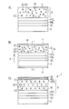
- FIGS. 1A and 1C show schematic sectional views of procedural steps for producing an embodiment of an organic light-emitting diode 1 .
- an electrode 33 a hole injection layer HIL as well as a hole transport layer HTL are applied to a carrier 3 , for example a glass plate.
- the electrode 33 is in particular an anode.
- Said anode is preferably shaped of a transparent conductive oxide, such as indium tin oxide.
- the hole injection layer HIL and the hole transport layer HTL are optional.
- a solution S is applied to a side of the hole transport layer HTL facing away from the carrier 3 .
- the solution S comprises a solvent L, a matrix material M, as well as three emitter materials E 1 , E 2 , E 3 .
- the solvent L is preferably a polar, hardly volatile and slowly vaporizing solvent, in which all components can be easily dissolved. Phenetole is used as a solvent, for example.
- a boiling point of the used solvent preferably equals at least 100° C. or 140° C., at normal pressure.
- a mass fraction of the components M, E 1 , E 2 , E 3 dissolved in the solvent L preferably equals between 0.1% and 1% inclusively.
- a layer thickness of the applied solution equals, for example, approximately 10 ⁇ m.
- the arrangement is applied between two field electrodes 4 , as shown in FIG. 1A .
- Said field electrodes 4 are set up to generate an electrical field F, preferably a static electrical field.
- An interval between the electrodes 4 is minimal and equals, for example, at least 1.5 mm or 2 mm or 3 mm and/or a maximum of 10 mm or 6 mm or 4 mm.
- the carrier 3 is in contact with one of the field electrodes 4 .
- the carrier 3 and the solution S are preferably separated from the field electrodes 4 by a gap.
- an electrical field is applied between the field electrodes 4 .
- a field strength equals, for example, a magnitude of 100 V/mm.
- the solution L is slowly volatilized during drying and baking. This results in a solid state layer, wherein the emitter materials E 1 , E 2 , E 3 are embedded in the matrix material M, so that a plurality of emitter layers 20 emerges.
- a mass fraction of the emitter materials E 1 , E 2 , E 3 on the emerging layer, once the solvent L is completely removed preferably equals at least 0.5% or 1% or 2% and, alternatively or additionally, a maximum of 7.5% or 5%.
- a predominant weight proportion of the resulting layer is formed by the matrix material M.
- matrix materials are used, as stated in the document US 2010/0059740 A1 or US 2013/0046096 A1. The disclosure of said documents in this respect is hereby incorporated by reference.
- the resulting, completed organic light-emitting diode 1 is shown in FIG. 1C .
- an electron transport layer ETL and an electron injection layer EIL is applied as an optional addition to the completed emitter layers 20 .
- the HIL, HTL, 20 , ETL, EIL layers form an organic layer stack 2 , in which the emitter layers 20 are embedded.
- a second electrode 33 in particular a metallic cathode, is applied. Additional layers of the organic light-emitting diode 1 , such an encapsulation layers, bus electrodes or electronic components are not illustrated for reasons of simplification.
- the three emitter layers 20 result due to the electrical field F applied during the drying of the solvent S, see also FIG. 1C .
- the negatively charged emitter material E 3 for example, is located nearest to the carrier 3 , followed by a neutral emitter material E 2 , for example, and followed thereafter by a positively charged emitter material E 1 .
- more than three emitter layers 20 are separated or that further functional layers are applied to the emitter layers 20 by means of the solution S. In such case, for example, single positively charged, two-fold positively charged and three-fold positively charged components etc. can be present in the solution S to be dried.
- the materials to be separated then arrange themselves in the electrical field F according to the different charges and/or ion mobilities.
- the individual emitter materials E 1 , E 2 , E 3 are in particular introduced into the solution S with the respectively associated counter ions.
- Said counter ions preferably have a lower, comparable or a not much higher mobility in the electrical field F in the solution S than the emitter materials E 1 , E 2 , E 3 .
- This enables said emitter materials E 1 , E 2 , E 3 to arrange themselves as desired in the electrical field F. This can, for example, be achieved by counter ions with a comparable or larger molecular size than the emitter materials E 1 , E 2 , E 3 .
- the light-emitting diode 1 according to FIG. 1C is set up to only emit radiation through the carrier 3 .
- the light-emitting diode 1 can be configured to emit on both sides or to only emit on a side facing the carrier 3 .
- the materials for said carrier 3 as well as the electrodes 33 are to be selected accordingly.
- FIG. 2 shows a further exemplary embodiment of the organic light-emitting diode 1 .
- Said light-emitting diode 1 according to FIG. 2 has only two of the emitter layers 20 .
- the emitter material E 1 is, for example, singly negatively charged and the emitter material E 2 can be electrically neutral and thus uncharged. This allows the counter ions C for the loaded emitter material E 1 to be located with the electrically neutral emitter material E 2 on a side of the layer facing away from the carrier 3 .
- An active zone with a plurality of emitter layers 20 can thus be generated with only a single solution S.
- the emitter layers 20 for generating blue light and yellow-orange light are set up in such a way as to generate white mixed light.
- the individual emitter materials are thereby only present in the associated emitter layer 20 in a demixed state.
- Such a production method thus allows an organic light-emitting diode with a plurality of emitter layers 20 to be generated by a single, wet-processing step and by a single, joint solvent in a joint matrix material. This enables any vaporization of individual layers, specifically in an active zone, to be avoided. This goes hand in hand with increased productivity and reduced costs.
- the emitter layers 20 need not be separated one after another, and can instead be separated in a single step. This joint separation allows any dissolution of previously already separated wet-processed layers to be avoided. This in turn allows the duration of the process to be reduced.
- this application opens up different ionic emitter materials to wet processing for generating the emitter layers.
- Os (II)-Triplet-Emitters can be used. It is thus enabled an optimization of the organic light-diode with regard to the used materials.
Landscapes
- Chemical & Material Sciences (AREA)
- Engineering & Computer Science (AREA)
- Manufacturing & Machinery (AREA)
- Materials Engineering (AREA)
- Physics & Mathematics (AREA)
- Optics & Photonics (AREA)
- Organic Chemistry (AREA)
- Crystallography & Structural Chemistry (AREA)
- Inorganic Chemistry (AREA)
- Electroluminescent Light Sources (AREA)
Abstract
Description

wherein M is selected from the group Mo, Ru, Rh, Pd, Ag, W, Re, Os, Ir, Pt, Cu, Au and lanthanides,
wherein the anion is freely selectable,
wherein the ligands
are formed independently of each other analogous to the imidazolinium substituted ligands “Ax-Spacer-Imidazol” or are selected from cyclo metallizing ligands,
wherein Ax, Ax′ is a substituted or unsubstituted aromatic or heteroaromatic, which is capable of forming bond relations to the metallic central atom M,
wherein a bond of the metallic central atom to a carbon or nitrogen of the Ax and of the Ax′ is illustrated by a solid line,
wherein a bond of the metallic central atom to either a carbene carbon or a nitrogen or phosphor coordinated by a free pair of electrons is represented by a dashed line,
wherein
a) aliphatic chains such as —(CH2)n— wherein n=1 to 20,
b) fluorinated alkyl chains with 1-12 carbon atoms in the chain,
c) unsaturated alkyl chains with 1-20 carbon atoms and conjugated or non-conjugated double bonds,
d) unsaturated alkyl chains with 1-20 carbon atoms and conjugated or non-conjugated triple bonds, also in conjunction with aromatics,
e) a polyethylene glycol, polyethylene diamine, polyester, polyurethane or polyvinylidene phenyl chain,
f) chains containing aromatics, or
g) mixed variants of a-f,
are used as spacers,
R1, R2, R+ are selected independently of each other from the following group: H, branched alkyl radicals, unbranched alkyl radicals, condensed alkyl radicals, cyclic alkyl radicals, fully or partially substituted unbranched, branched, condensed and/or cyclic alkyl radicals, alkoxy groups, amines, amides, ester, ether, carbonate, aromatics, fully or partially substituted aromatics, heteroaromatics, condensed aromatics, fully or partially substituted condensed aromatics, heterocycles, fully or partially substituted heterocycles, condensed heterocycles, halogens, pseudohalogen, condensed alkyl radicals or fully or partially substituted alkyl radicals.


R, X are selected independently of each other from the following group: H, branched alkyl radicals, unbranched alkyl radicals, condensed alkyl radicals, cyclic alkyl radicals, fully or partially substituted unbranched, branched, condensed and/or cyclic alkyl radicals, alkoxy groups, amines, amides, ester, ether, carbonate, aromatics, fully or partially substituted aromatics, heteroaromatics, condensed aromatics, fully or partially substituted condensed aromatics, heterocycles, fully or partially substituted heterocycles, condensed heterocycles, halogens, pseudohalogen, condensed alkyl radicals or fully or partially substituted alkyl radicals. The charged residue groups —PBu3 + can be replaced independently of each other by other charged residue groups, such as —NR3 +, —P(R)3 +, —COO−, —P(OR)4 2−. Furthermore, Ir as well as Os can be replaced by Mo, Ru, Rh, Pd, Ag, W, Re, Pt, Cu, Au and lanthanide. Other counter ions can also be used instead of PF6 −.
Claims (11)


Applications Claiming Priority (4)
| Application Number | Priority Date | Filing Date | Title |
|---|---|---|---|
| DE102014101650.5A DE102014101650B4 (en) | 2014-02-11 | 2014-02-11 | Process for the production of an organic light-emitting diode and organic light-emitting diode |
| DE102014101650.5 | 2014-02-11 | ||
| DE102014101650 | 2014-02-11 | ||
| PCT/EP2015/052747 WO2015121247A1 (en) | 2014-02-11 | 2015-02-10 | Method for producing an organic light-emitting diode, and organic light-emitting diode |
Publications (2)
| Publication Number | Publication Date |
|---|---|
| US20160359127A1 US20160359127A1 (en) | 2016-12-08 |
| US10177331B2 true US10177331B2 (en) | 2019-01-08 |
Family
ID=52484461
Family Applications (1)
| Application Number | Title | Priority Date | Filing Date |
|---|---|---|---|
| US15/118,086 Active 2035-05-05 US10177331B2 (en) | 2014-02-11 | 2015-02-10 | Method for producing an organic light-emitting diode, and organic light-emitting diode |
Country Status (3)
| Country | Link |
|---|---|
| US (1) | US10177331B2 (en) |
| DE (1) | DE102014101650B4 (en) |
| WO (1) | WO2015121247A1 (en) |
Families Citing this family (3)
| Publication number | Priority date | Publication date | Assignee | Title |
|---|---|---|---|---|
| KR102088883B1 (en) * | 2013-12-02 | 2020-03-16 | 엘지디스플레이 주식회사 | Organic Light Emitting Display Device |
| KR102344729B1 (en) * | 2014-12-15 | 2021-12-31 | 엘지디스플레이 주식회사 | Organic Light Emitting Display Device |
| CN107591491A (en) * | 2017-07-26 | 2018-01-16 | 佛山科学技术学院 | A kind of undoped white-light emitting layer series connection organic electroluminescence device and preparation method thereof |
Citations (6)
| Publication number | Priority date | Publication date | Assignee | Title |
|---|---|---|---|---|
| US4839032A (en) * | 1986-06-06 | 1989-06-13 | Advanced Energy Dynamics Inc. | Separating constituents of a mixture of particles |
| US20090050199A1 (en) | 2007-08-21 | 2009-02-26 | Washington, University Of | Semiconducting polymer films with fixed electronic junctions |
| US20100059740A1 (en) | 2007-01-17 | 2010-03-11 | Merck Patent Gmbh | Polymeric anions/cations |
| US20100173134A1 (en) * | 2008-06-26 | 2010-07-08 | Carben Semicon Limited | Film and Device Using Layer Based on Ribtan Material |
| US20120169213A1 (en) | 2009-07-03 | 2012-07-05 | Osram Ag | Phosphorescent metal complex compound, method for the production thereof and radiation emitting structural element |
| US20130046096A1 (en) | 2010-01-25 | 2013-02-21 | Osram Opto Semiconductors Gmbh | Phosphorescent Metal Complex, Process for Production and Light-Emitting Component |
Family Cites Families (1)
| Publication number | Priority date | Publication date | Assignee | Title |
|---|---|---|---|---|
| DE102011017572A1 (en) | 2011-04-27 | 2012-10-31 | Siemens Aktiengesellschaft | Component with oriented organic semiconductor |
-
2014
- 2014-02-11 DE DE102014101650.5A patent/DE102014101650B4/en active Active
-
2015
- 2015-02-10 US US15/118,086 patent/US10177331B2/en active Active
- 2015-02-10 WO PCT/EP2015/052747 patent/WO2015121247A1/en not_active Ceased
Patent Citations (6)
| Publication number | Priority date | Publication date | Assignee | Title |
|---|---|---|---|---|
| US4839032A (en) * | 1986-06-06 | 1989-06-13 | Advanced Energy Dynamics Inc. | Separating constituents of a mixture of particles |
| US20100059740A1 (en) | 2007-01-17 | 2010-03-11 | Merck Patent Gmbh | Polymeric anions/cations |
| US20090050199A1 (en) | 2007-08-21 | 2009-02-26 | Washington, University Of | Semiconducting polymer films with fixed electronic junctions |
| US20100173134A1 (en) * | 2008-06-26 | 2010-07-08 | Carben Semicon Limited | Film and Device Using Layer Based on Ribtan Material |
| US20120169213A1 (en) | 2009-07-03 | 2012-07-05 | Osram Ag | Phosphorescent metal complex compound, method for the production thereof and radiation emitting structural element |
| US20130046096A1 (en) | 2010-01-25 | 2013-02-21 | Osram Opto Semiconductors Gmbh | Phosphorescent Metal Complex, Process for Production and Light-Emitting Component |
Non-Patent Citations (5)
| Title |
|---|
| Bolink, H. et al., "Green Light-Emitting Solid-State Electrocherncial Cell Obtained from a Homoleptic Iridium (III) Complex Containing Ionically Charged Ligands", Journal of the American Chemical Society, vol. 18, 2006, No. 12, pp. 2778-2780. |
| Carlson, B. et al., "Divalent Osmium Complexes: Synthesis, Characterization, Strong Red Phosphorescence, and Electrophosphorescence", Journal of the American Chemical Society, vol. 124, 2002, No. 47, pp. 14162-14172. |
| He, L. et al, "Highly Efficient Blue-Green and White Light-Emitting Electrochemical Cells Based on a Cationic Iridium Complex with a Bulky Side Group", Chemistry of Materials, vol. 22, 2010, No. 11, pp. 3535-3542. |
| Zhen C. et al. , Incorporation of electroluminescence and electrochemiluminescence in one organic light-emitting device, Applied Physics Letters, Aug. 2005, 87, 093508. * |
| Zhen, C. et al, "Incorporation of Electroluminescence and Electrochemiluminescence in One Organic Light-Emitting Device", Appl. Phys. Lett., 87, 2005, pp. 093508-1-093508-3. |
Also Published As
| Publication number | Publication date |
|---|---|
| WO2015121247A1 (en) | 2015-08-20 |
| DE102014101650A1 (en) | 2015-08-13 |
| US20160359127A1 (en) | 2016-12-08 |
| DE102014101650B4 (en) | 2021-07-08 |
Similar Documents
| Publication | Publication Date | Title |
|---|---|---|
| US12096681B2 (en) | Organic electroluminescent materials and devices | |
| US11228010B2 (en) | Organic electroluminescent materials and devices | |
| US10862046B2 (en) | Organic electroluminescent materials and devices | |
| US20230225205A1 (en) | Organic electroluminescent materials and devices | |
| US12010859B2 (en) | Organic electroluminescent materials and devices | |
| EP3547387B1 (en) | Electroluminescent element | |
| US11183646B2 (en) | Organic electroluminescent materials and devices | |
| US12391876B2 (en) | Organic electroluminescent materials and devices | |
| CN102844402B (en) | Phosphorescent metal complex compounds, for manufacturing its method and luminescent device | |
| US20180026208A1 (en) | Organic electroluminescent materials and devices | |
| US11322691B2 (en) | Organic electroluminescent materials and devices | |
| JP6549434B2 (en) | Method of manufacturing organic electroluminescent device | |
| US20170309838A1 (en) | Organic electroluminescent materials and devices | |
| US10177331B2 (en) | Method for producing an organic light-emitting diode, and organic light-emitting diode | |
| US12098157B2 (en) | Organic electroluminescent materials and devices | |
| US20220352478A1 (en) | Organic eletroluminescent materials and devices | |
| US11139443B2 (en) | Organic electroluminescent materials and devices | |
| US20210028376A1 (en) | Organic electroluminescent materials and devices | |
| JP2015069714A (en) | Organic electroluminescence device | |
| US11608321B2 (en) | Organic electroluminescent materials and devices | |
| US11081647B2 (en) | Organic electroluminescent materials and devices | |
| US20240306409A1 (en) | Organic electroluminescent materials and devices | |
| JP5922654B2 (en) | Organic electroluminescent device | |
| WO2014084206A1 (en) | Organic el element | |
| US20240373661A1 (en) | Phosphorescent OLED with inorganic host materials |
Legal Events
| Date | Code | Title | Description |
|---|---|---|---|
| AS | Assignment |
Owner name: OSRAM OLED GMBH, GERMANY Free format text: ASSIGNMENT OF ASSIGNORS INTEREST;ASSIGNORS:SCHARNER, SILKE;DIEZ, CAROLA;PENTLEHNER, DOMINIK;AND OTHERS;SIGNING DATES FROM 20160823 TO 20160907;REEL/FRAME:040106/0526 |
|
| STCF | Information on status: patent grant |
Free format text: PATENTED CASE |
|
| AS | Assignment |
Owner name: PICTIVA DISPLAYS INTERNATIONAL LIMITED, IRELAND Free format text: CORRECTIVE ASSIGNMENT TO CORRECT THE 11/658.772 REPLACED 11/658.772 PROPERTY NUMBERS PREVIOUSLY RECORDED AT REEL: 053464 FRAME: 0395. ASSIGNOR(S) HEREBY CONFIRMS THE ASSIGNMENT;ASSIGNOR:DOLYA HOLDCO 5 LIMITED;REEL/FRAME:053464/0395 Effective date: 20200717 Owner name: PICTIVA DISPLAYS INTERNATIONAL LIMITED, IRELAND Free format text: CHANGE OF NAME;ASSIGNOR:DOLYA HOLDCO 5 LIMITED;REEL/FRAME:053464/0395 Effective date: 20200717 Owner name: DOLYA HOLDCO 5 LIMITED, IRELAND Free format text: ASSIGNMENT OF ASSIGNORS INTEREST;ASSIGNOR:OSRAM OLED GMBH;REEL/FRAME:053464/0374 Effective date: 20200703 |
|
| MAFP | Maintenance fee payment |
Free format text: PAYMENT OF MAINTENANCE FEE, 4TH YEAR, LARGE ENTITY (ORIGINAL EVENT CODE: M1551); ENTITY STATUS OF PATENT OWNER: LARGE ENTITY Year of fee payment: 4 |