US10176996B2 - Replacement metal gate and fabrication process with reduced lithography steps - Google Patents
Replacement metal gate and fabrication process with reduced lithography steps Download PDFInfo
- Publication number
- US10176996B2 US10176996B2 US14/452,606 US201414452606A US10176996B2 US 10176996 B2 US10176996 B2 US 10176996B2 US 201414452606 A US201414452606 A US 201414452606A US 10176996 B2 US10176996 B2 US 10176996B2
- Authority
- US
- United States
- Prior art keywords
- pfet
- lct
- sct
- nfet
- layer
- Prior art date
- Legal status (The legal status is an assumption and is not a legal conclusion. Google has not performed a legal analysis and makes no representation as to the accuracy of the status listed.)
- Active, expires
Links
Images


Classifications
-
- H—ELECTRICITY
- H01—ELECTRIC ELEMENTS
- H01L—SEMICONDUCTOR DEVICES NOT COVERED BY CLASS H10
- H01L21/00—Processes or apparatus adapted for the manufacture or treatment of semiconductor or solid state devices or of parts thereof
- H01L21/02—Manufacture or treatment of semiconductor devices or of parts thereof
- H01L21/04—Manufacture or treatment of semiconductor devices or of parts thereof the devices having potential barriers, e.g. a PN junction, depletion layer or carrier concentration layer
- H01L21/18—Manufacture or treatment of semiconductor devices or of parts thereof the devices having potential barriers, e.g. a PN junction, depletion layer or carrier concentration layer the devices having semiconductor bodies comprising elements of Group IV of the Periodic Table or AIIIBV compounds with or without impurities, e.g. doping materials
- H01L21/28—Manufacture of electrodes on semiconductor bodies using processes or apparatus not provided for in groups H01L21/20 - H01L21/268
- H01L21/28008—Making conductor-insulator-semiconductor electrodes
- H01L21/28017—Making conductor-insulator-semiconductor electrodes the insulator being formed after the semiconductor body, the semiconductor being silicon
- H01L21/28026—Making conductor-insulator-semiconductor electrodes the insulator being formed after the semiconductor body, the semiconductor being silicon characterised by the conductor
- H01L21/28123—Lithography-related aspects, e.g. sub-lithography lengths; Isolation-related aspects, e.g. to solve problems arising at the crossing with the side of the device isolation; Planarisation aspects
-
- H10D64/01326—
-
- H—ELECTRICITY
- H01—ELECTRIC ELEMENTS
- H01L—SEMICONDUCTOR DEVICES NOT COVERED BY CLASS H10
- H01L21/00—Processes or apparatus adapted for the manufacture or treatment of semiconductor or solid state devices or of parts thereof
- H01L21/02—Manufacture or treatment of semiconductor devices or of parts thereof
- H01L21/04—Manufacture or treatment of semiconductor devices or of parts thereof the devices having potential barriers, e.g. a PN junction, depletion layer or carrier concentration layer
- H01L21/18—Manufacture or treatment of semiconductor devices or of parts thereof the devices having potential barriers, e.g. a PN junction, depletion layer or carrier concentration layer the devices having semiconductor bodies comprising elements of Group IV of the Periodic Table or AIIIBV compounds with or without impurities, e.g. doping materials
- H01L21/28—Manufacture of electrodes on semiconductor bodies using processes or apparatus not provided for in groups H01L21/20 - H01L21/268
- H01L21/28008—Making conductor-insulator-semiconductor electrodes
- H01L21/28017—Making conductor-insulator-semiconductor electrodes the insulator being formed after the semiconductor body, the semiconductor being silicon
- H01L21/28026—Making conductor-insulator-semiconductor electrodes the insulator being formed after the semiconductor body, the semiconductor being silicon characterised by the conductor
- H01L21/28088—Making conductor-insulator-semiconductor electrodes the insulator being formed after the semiconductor body, the semiconductor being silicon characterised by the conductor the final conductor layer next to the insulator being a composite, e.g. TiN
-
- H—ELECTRICITY
- H01—ELECTRIC ELEMENTS
- H01L—SEMICONDUCTOR DEVICES NOT COVERED BY CLASS H10
- H01L21/00—Processes or apparatus adapted for the manufacture or treatment of semiconductor or solid state devices or of parts thereof
- H01L21/02—Manufacture or treatment of semiconductor devices or of parts thereof
- H01L21/04—Manufacture or treatment of semiconductor devices or of parts thereof the devices having potential barriers, e.g. a PN junction, depletion layer or carrier concentration layer
- H01L21/18—Manufacture or treatment of semiconductor devices or of parts thereof the devices having potential barriers, e.g. a PN junction, depletion layer or carrier concentration layer the devices having semiconductor bodies comprising elements of Group IV of the Periodic Table or AIIIBV compounds with or without impurities, e.g. doping materials
- H01L21/30—Treatment of semiconductor bodies using processes or apparatus not provided for in groups H01L21/20 - H01L21/26
- H01L21/31—Treatment of semiconductor bodies using processes or apparatus not provided for in groups H01L21/20 - H01L21/26 to form insulating layers thereon, e.g. for masking or by using photolithographic techniques; After treatment of these layers; Selection of materials for these layers
- H01L21/3205—Deposition of non-insulating-, e.g. conductive- or resistive-, layers on insulating layers; After-treatment of these layers
- H01L21/321—After treatment
- H01L21/3213—Physical or chemical etching of the layers, e.g. to produce a patterned layer from a pre-deposited extensive layer
- H01L21/32139—Physical or chemical etching of the layers, e.g. to produce a patterned layer from a pre-deposited extensive layer using masks
-
- H01L21/823842—
-
- H01L21/82385—
-
- H01L21/823857—
-
- H01L27/0922—
-
- H01L29/4966—
-
- H01L29/66545—
-
- H10D64/01318—
-
- H—ELECTRICITY
- H10—SEMICONDUCTOR DEVICES; ELECTRIC SOLID-STATE DEVICES NOT OTHERWISE PROVIDED FOR
- H10D—INORGANIC ELECTRIC SEMICONDUCTOR DEVICES
- H10D64/00—Electrodes of devices having potential barriers
- H10D64/01—Manufacture or treatment
- H10D64/017—Manufacture or treatment using dummy gates in processes wherein at least parts of the final gates are self-aligned to the dummy gates, i.e. replacement gate processes
-
- H—ELECTRICITY
- H10—SEMICONDUCTOR DEVICES; ELECTRIC SOLID-STATE DEVICES NOT OTHERWISE PROVIDED FOR
- H10D—INORGANIC ELECTRIC SEMICONDUCTOR DEVICES
- H10D64/00—Electrodes of devices having potential barriers
- H10D64/60—Electrodes characterised by their materials
- H10D64/66—Electrodes having a conductor capacitively coupled to a semiconductor by an insulator, e.g. MIS electrodes
- H10D64/667—Electrodes having a conductor capacitively coupled to a semiconductor by an insulator, e.g. MIS electrodes the conductor comprising a layer of alloy material, compound material or organic material contacting the insulator, e.g. TiN workfunction layers
-
- H—ELECTRICITY
- H10—SEMICONDUCTOR DEVICES; ELECTRIC SOLID-STATE DEVICES NOT OTHERWISE PROVIDED FOR
- H10D—INORGANIC ELECTRIC SEMICONDUCTOR DEVICES
- H10D84/00—Integrated devices formed in or on semiconductor substrates that comprise only semiconducting layers, e.g. on Si wafers or on GaAs-on-Si wafers
- H10D84/01—Manufacture or treatment
- H10D84/0123—Integrating together multiple components covered by H10D12/00 or H10D30/00, e.g. integrating multiple IGBTs
- H10D84/0126—Integrating together multiple components covered by H10D12/00 or H10D30/00, e.g. integrating multiple IGBTs the components including insulated gates, e.g. IGFETs
- H10D84/0165—Integrating together multiple components covered by H10D12/00 or H10D30/00, e.g. integrating multiple IGBTs the components including insulated gates, e.g. IGFETs the components including complementary IGFETs, e.g. CMOS devices
- H10D84/0172—Manufacturing their gate conductors
- H10D84/0177—Manufacturing their gate conductors the gate conductors having different materials or different implants
-
- H—ELECTRICITY
- H10—SEMICONDUCTOR DEVICES; ELECTRIC SOLID-STATE DEVICES NOT OTHERWISE PROVIDED FOR
- H10D—INORGANIC ELECTRIC SEMICONDUCTOR DEVICES
- H10D84/00—Integrated devices formed in or on semiconductor substrates that comprise only semiconducting layers, e.g. on Si wafers or on GaAs-on-Si wafers
- H10D84/01—Manufacture or treatment
- H10D84/0123—Integrating together multiple components covered by H10D12/00 or H10D30/00, e.g. integrating multiple IGBTs
- H10D84/0126—Integrating together multiple components covered by H10D12/00 or H10D30/00, e.g. integrating multiple IGBTs the components including insulated gates, e.g. IGFETs
- H10D84/0165—Integrating together multiple components covered by H10D12/00 or H10D30/00, e.g. integrating multiple IGBTs the components including insulated gates, e.g. IGFETs the components including complementary IGFETs, e.g. CMOS devices
- H10D84/0172—Manufacturing their gate conductors
- H10D84/0179—Manufacturing their gate conductors the gate conductors having different shapes or dimensions
-
- H—ELECTRICITY
- H10—SEMICONDUCTOR DEVICES; ELECTRIC SOLID-STATE DEVICES NOT OTHERWISE PROVIDED FOR
- H10D—INORGANIC ELECTRIC SEMICONDUCTOR DEVICES
- H10D84/00—Integrated devices formed in or on semiconductor substrates that comprise only semiconducting layers, e.g. on Si wafers or on GaAs-on-Si wafers
- H10D84/01—Manufacture or treatment
- H10D84/0123—Integrating together multiple components covered by H10D12/00 or H10D30/00, e.g. integrating multiple IGBTs
- H10D84/0126—Integrating together multiple components covered by H10D12/00 or H10D30/00, e.g. integrating multiple IGBTs the components including insulated gates, e.g. IGFETs
- H10D84/0165—Integrating together multiple components covered by H10D12/00 or H10D30/00, e.g. integrating multiple IGBTs the components including insulated gates, e.g. IGFETs the components including complementary IGFETs, e.g. CMOS devices
- H10D84/0181—Manufacturing their gate insulating layers
-
- H—ELECTRICITY
- H10—SEMICONDUCTOR DEVICES; ELECTRIC SOLID-STATE DEVICES NOT OTHERWISE PROVIDED FOR
- H10D—INORGANIC ELECTRIC SEMICONDUCTOR DEVICES
- H10D84/00—Integrated devices formed in or on semiconductor substrates that comprise only semiconducting layers, e.g. on Si wafers or on GaAs-on-Si wafers
- H10D84/01—Manufacture or treatment
- H10D84/02—Manufacture or treatment characterised by using material-based technologies
- H10D84/03—Manufacture or treatment characterised by using material-based technologies using Group IV technology, e.g. silicon technology or silicon-carbide [SiC] technology
- H10D84/038—Manufacture or treatment characterised by using material-based technologies using Group IV technology, e.g. silicon technology or silicon-carbide [SiC] technology using silicon technology, e.g. SiGe
-
- H—ELECTRICITY
- H10—SEMICONDUCTOR DEVICES; ELECTRIC SOLID-STATE DEVICES NOT OTHERWISE PROVIDED FOR
- H10D—INORGANIC ELECTRIC SEMICONDUCTOR DEVICES
- H10D84/00—Integrated devices formed in or on semiconductor substrates that comprise only semiconducting layers, e.g. on Si wafers or on GaAs-on-Si wafers
- H10D84/80—Integrated devices formed in or on semiconductor substrates that comprise only semiconducting layers, e.g. on Si wafers or on GaAs-on-Si wafers characterised by the integration of at least one component covered by groups H10D12/00 or H10D30/00, e.g. integration of IGFETs
- H10D84/82—Integrated devices formed in or on semiconductor substrates that comprise only semiconducting layers, e.g. on Si wafers or on GaAs-on-Si wafers characterised by the integration of at least one component covered by groups H10D12/00 or H10D30/00, e.g. integration of IGFETs of only field-effect components
- H10D84/83—Integrated devices formed in or on semiconductor substrates that comprise only semiconducting layers, e.g. on Si wafers or on GaAs-on-Si wafers characterised by the integration of at least one component covered by groups H10D12/00 or H10D30/00, e.g. integration of IGFETs of only field-effect components of only insulated-gate FETs [IGFET]
- H10D84/85—Complementary IGFETs, e.g. CMOS
- H10D84/856—Complementary IGFETs, e.g. CMOS the complementary IGFETs having different architectures than each other, e.g. high-voltage and low-voltage CMOS
-
- H10P50/71—
-
- H01L29/517—
-
- H—ELECTRICITY
- H10—SEMICONDUCTOR DEVICES; ELECTRIC SOLID-STATE DEVICES NOT OTHERWISE PROVIDED FOR
- H10D—INORGANIC ELECTRIC SEMICONDUCTOR DEVICES
- H10D64/00—Electrodes of devices having potential barriers
- H10D64/60—Electrodes characterised by their materials
- H10D64/66—Electrodes having a conductor capacitively coupled to a semiconductor by an insulator, e.g. MIS electrodes
- H10D64/68—Electrodes having a conductor capacitively coupled to a semiconductor by an insulator, e.g. MIS electrodes characterised by the insulator, e.g. by the gate insulator
- H10D64/691—Electrodes having a conductor capacitively coupled to a semiconductor by an insulator, e.g. MIS electrodes characterised by the insulator, e.g. by the gate insulator comprising metallic compounds, e.g. metal oxides or metal silicates
Definitions
- the present invention relates generally to semiconductor fabrication, and more particularly, to a replacement metal gate and fabrication process.
- a replacement metal gate In a replacement metal gate (RMG), or “gate last” process, the polysilicon gate is replaced with a metal gate stack.
- P-type field effect transistors (PFETs) and N-type field effect transistors (NFETs) utilize different metal stacks to achieve a desired work function, and thus enable a desired threshold voltage.
- PFETs P-type field effect transistors
- NFETs N-type field effect transistors
- the use of different metals in adjacent devices typically requires numerous, time-consuming steps to fabricate them. Therefore, it is desirable to have improvements in replacement metal gates and fabrication methods to reduce time and cost of fabrication.
- Embodiments of the present invention provide a replacement metal gate and a fabrication process with reduced lithography steps. Using selective etching techniques, a layer of fill metal is used to protect the dielectric layer in the trenches, eliminating the need for some lithography steps. This, in turn, reduces the overall cost and complexity of fabrication. Furthermore, additional protection is provided during etching, which serves to improve product yield.
- embodiments of the present invention provide a method of forming a semiconductor structure, comprising: forming an nFET short channel trench (SCT), a pFET SCT, an nFET long channel trench (LCT), and a pFET LCT in a dielectric layer that is disposed on a semiconductor substrate; depositing a high-K dielectric layer in the nFET SCT, pFET SCT, nFET LCT, and pFET LCT; depositing an N type work function metal in the nFET SCT, pFET SCT, nFET LCT, and the pFET LCT; performing a high-K dielectric chamfer process on the nFET SCT and pFET SCT; depositing a metal layer in the nFET SCT, pFET SCT, nFET LCT, and the pFET LCT, such that the metal layer is deposited conformally in the nFET LCT and the
- embodiments of the present invention provide a method of forming a semiconductor structure, comprising: forming an nFET short channel trench (SCT), a pFET SCT, an nFET long channel trench (LCT), and a pFET LCT in a dielectric layer that is disposed on a semiconductor substrate; depositing a high-K dielectric layer in the nFET SCT, pFET SCT, nFET LCT, and pFET LCT; depositing an N type work function metal in the nFET SCT, pFET SCT, nFET LCT, and pFET LCT; performing a high-K dielectric chamfer process on the nFET SCT and pFET SCT; depositing a metal layer in the nFET SCT, pFET SCT, nFET LCT, and pFET LCT, such that the metal layer is deposited conformally in the nFET LCT and a p
- embodiments of the present invention provide A semiconductor structure comprising: an nFET short channel trench (SCT); a pFET SCT; an nFET long channel trench (LCT); a pFET LCT; wherein the nFET LCT comprises: a high-K dielectric layer disposed along a bottom surface of the nFET LCT; an n-type work function material layer disposed on the high-K dielectric layer; a first tungsten layer disposed on the n-type work function material layer; a titanium nitride layer disposed on the first tungsten layer; a second tungsten layer disposed on the titanium nitride layer; and a capping layer disposed on the second tungsten layer.
- SCT nFET short channel trench
- LCT nFET long channel trench
- LCT pFET LCT
- the nFET LCT comprises: a high-K dielectric layer disposed along a bottom surface of the nFET LCT; an
- cross-sectional views may be in the form of “slices”, or “near-sighted” cross-sectional views, omitting certain background lines which would otherwise be visible in a “true” cross-sectional view, for illustrative clarity.
- FIG. 1A is a semiconductor structure at a starting point for embodiments of the present invention.
- FIG. 1B is a semiconductor structure after a subsequent process step of depositing a metal layer.
- FIG. 1C is a semiconductor structure after a subsequent process step of depositing an organic planarization layer.
- FIG. 1D is a semiconductor structure after a subsequent process step of recessing the organic planarization layer material.
- FIG. 1E is a semiconductor structure after a subsequent process step of recessing the metal layer.
- FIG. 1F is a semiconductor structure after a subsequent process step of depositing additional organic planarization material.
- FIG. 1G is a semiconductor structure after a subsequent process step of performing a partial recess of the organic planarization layer.
- FIG. 1H is a semiconductor structure after a subsequent process step of performing a partial recess of the n-type work function metal.
- FIG. 1 i is a semiconductor structure after a subsequent process step of depositing an additional lithography stack.
- FIG. 1J is a semiconductor structure after a subsequent process step of opening the lithography stack over the PFET trenches.
- FIG. 1K is a semiconductor structure after a subsequent process step of removing the lithography stack in the PFET trenches.
- FIG. 1L is a semiconductor structure after a subsequent process step of removing the n-type work function metal in the PFET trenches.
- FIG. 1M is a semiconductor structure after a subsequent process step of removing the remaining organic planarization layer.
- FIG. 1N is a semiconductor structure after a subsequent process step of depositing a p-type work function metal.
- FIG. 1 o is a semiconductor structure after a subsequent process step of depositing a gate fill metal.
- FIG. 1P is a semiconductor structure after a subsequent process step of recessing the gate fill metal.
- FIG. 1Q is a semiconductor structure after a subsequent process step of depositing a capping layer.
- FIG. 2A is a semiconductor structure at a starting point for additional embodiments of the present invention, following from FIG. 1D .
- FIG. 2B is a semiconductor structure after a subsequent process step of removing the remaining organic planarization layer.
- FIG. 2C is a semiconductor structure after a subsequent process step of depositing a lithography stack.
- FIG. 2D is a semiconductor structure after a subsequent process step of opening the lithography stack over the PFET trenches.
- FIG. 2E is a semiconductor structure after a subsequent process step of removing the n-type work function metal in the PFET trenches.
- FIG. 2F is a semiconductor structure after a subsequent process step of removing the remaining organic planarization layer.
- FIG. 2G is a semiconductor structure after a subsequent process step of depositing a p-type work function metal.
- FIG. 2H is a semiconductor structure after a subsequent process step of depositing a gate fill metal.
- FIG. 2 i is a semiconductor structure after a subsequent process step of recessing the gate fill metal.
- FIG. 2J is a semiconductor structure after a subsequent process step of depositing a capping layer.
- FIG. 3A is a semiconductor structure at a starting point for additional embodiments of the present invention.
- FIG. 3B is a semiconductor structure after a subsequent process step of depositing a titanium nitride layer.
- FIG. 3C is a semiconductor structure after a subsequent process step of depositing a metal layer.
- FIG. 3D is a semiconductor structure after a subsequent process step of depositing an organic planarization layer.
- FIG. 3E is a semiconductor structure after a subsequent process step of recessing the metal layer and titanium nitride layer.
- FIG. 3F is a semiconductor structure after a subsequent process step of removing the remaining organic planarization layer.
- FIG. 3G is a semiconductor structure after a subsequent process step of recessing the high-K dielectric layer.
- FIG. 3H is a semiconductor structure after a subsequent process step of removing the remaining metal layer and titanium nitride layer.
- FIG. 4A is a semiconductor structure at a starting point for additional embodiments of the present invention.
- FIG. 4B is a semiconductor structure after a subsequent process step of depositing a titanium nitride layer and metal layer.
- FIG. 4C is a semiconductor structure after a subsequent process step of depositing a lithography stack.
- FIG. 4D is a semiconductor structure after a subsequent process step of opening the lithography stack over the PFET trenches.
- FIG. 4E is a semiconductor structure after a subsequent process step of removing the organic planarization layer in the PFET trenches.
- FIG. 4F is a semiconductor structure after a subsequent process step of removing the metal layer in the PFET trenches.
- FIG. 4G is a semiconductor structure after a subsequent process step of removing the n-type work function metal in the PFET trenches.
- FIG. 4H is a semiconductor structure after a subsequent process step of removing the remaining organic planarization layer.
- FIG. 4 i is a semiconductor structure after a subsequent process step of depositing a p-type work function metal.
- FIG. 4J is a semiconductor structure after a subsequent process step of depositing a gate fill metal.
- FIG. 4K is a semiconductor structure after a subsequent process step of recessing the gate fill metal.
- FIG. 4L is a semiconductor structure after a subsequent process step of depositing a capping layer.
- FIG. 5 is a flowchart for embodiments of the present invention.
- FIG. 6 is a flowchart for additional embodiments of the present invention.
- first element such as a first structure, e.g., a first layer
- second element such as a second structure, e.g. a second layer
- intervening elements such as an interface structure, e.g. interface layer
- depositing may include any now known or later developed techniques appropriate for the material to be deposited including, but not limited to, for example: chemical vapor deposition (CVD), low-pressure CVD (LPCVD), plasma-enhanced CVD (PECVD), sub-atmospheric CVD (SACVD) and high density plasma CVD (HDPCVD), rapid thermal CVD (RTCVD), ultra-high vacuum CVD (UHVCVD), limited reaction processing CVD (LRPCVD), metal-organic CVD (MOCVD), sputtering deposition, ion beam deposition, electron beam deposition, laser assisted deposition, thermal oxidation, thermal nitridation, spin-on methods, physical vapor deposition (PVD), atomic layer deposition (ALD), chemical oxidation, molecular beam epitaxy (MBE), plating, evaporation.
- CVD chemical vapor deposition
- LPCVD low-pressure CVD
- PECVD plasma-enhanced CVD
- SACVD
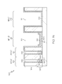
- FIG. 1A is a semiconductor structure 100 at a starting point for embodiments of the present invention.
- Semiconductor structure 100 comprises semiconductor substrate 102 .
- semiconductor substrate 102 comprises a silicon substrate.
- Substrate 102 may be a bulk silicon substrate or a semiconductor-on-insulator (SOI) semiconductor substrate.
- a dielectric layer 104 is formed on the semiconductor substrate 102 .
- the dielectric layer 104 is comprised of silicon oxide.
- a plurality of trenches are formed in the dielectric layer 104 , which include an n-type field effect transistor (nFET) short channel trench (SCT) 122 , p-type field effect transistor (pFET) SCT 124 , nFET long channel trench (LCT) 126 , and/or a pFET LCT 128 .
- the short channel trenches 122 and 124 have a width W 1 , which may or may not be uniform among all of the short channel trenches 122 , 124 . In embodiments, W 1 ranges from about 20 nanometers to about 40 nanometers.
- the long channel trenches 126 and 128 have a width W 2 , which also may or may not be uniform among all of the long channel trenches 126 , 128 . In embodiments, W 2 ranges from about 45 nanometers to about 500 nanometers.
- a corresponding cavity is present for each trench. Trench 122 has cavity 106 , trench 124 has cavity 108 , trench 126 has cavity 110 , and trench 128 has cavity 112 .
- a layer of high-K dielectric 116 lines the trench 126 and 128 .
- the high-K dielectric 116 is also in a lower, chamfered region 120 of trench 122 and trench 124 , while the high-K dielectric is not present in an upper, non-chamfered region 118 of the trench 122 and trench 124 .
- An n-type work function material (nWFM) 114 is disposed on the high-K dielectric layer 116 and non-chamfered region 118 of the trench 122 and trench 124 .
- the high-K dielectric layer is comprised of hafnium oxide.
- the high-K dielectric layer is comprised of zirconium oxide.
- the nWFM 114 may be comprised of titanium nitride.
- the nWFM 114 may be comprised of a multi-layer stack (not shown) of a first layer of titanium nitride, a layer of titanium carbide, and a second layer of titanium nitride.
- FIG. 1B is a semiconductor structure 100 after a subsequent process step of depositing a metal layer 130 .
- metal layer 130 is comprised of tungsten.
- the metal layer 130 deposits conformally on the long channel trenches 126 and 128 .
- the deposition of metal layer 130 fills the trenches 122 and 124 .
- FIG. 1C is a semiconductor structure 100 after a subsequent process step of depositing an organic planarization layer (OPL) 132 .
- the OPL 132 may include a photo-sensitive organic polymer comprising a light-sensitive material that, when exposed to electromagnetic radiation, is chemically altered and thus configured to be removed using a developing solvent.
- the photo-sensitive organic polymer may be polyacrylate resin, epoxy resin, phenol resin, polyamide resin, polyimide resin, unsaturated polyester resin, polyphenylenether resin, polyphenylenesulfide resin, or benzocyclobutene (BCB).
- FIG. 1D is a semiconductor structure 100 after a subsequent process step of recessing the organic planarization layer material 132 to a distance W 3 below the top of metal layer 130 .
- W 3 ranges from about 10 nanometers to about 20 nanometers.
- FIG. 1E is a semiconductor structure 100 after a subsequent process step of recessing the metal layer 130 .
- the recess of metal layer 130 may be performed by a fluorine-based wet etch process.
- metal region 130 A remains in the chamfered region 120 of trench 122
- metal region 130 B remains in the chamfered region 120 of trench 124
- metal region 130 C remains in the lower regions of trench 126
- metal region 130 D remains in the lower regions of trench 128 .
- a narrow trench 134 and 136 are formed on the sides of the long channel trenches 126 and 128 between the OPL 132 and the nWFM 114 .
- the narrow trenches 134 and 136 may have a width of the same order of magnitude as W 1 of the short channel trenches 122 and 124 .
- FIG. 1F is a semiconductor structure 100 after a subsequent process step of depositing additional organic planarization material 132 to fill the narrow trench 134 and 136 .
- the original organic planarization layer may be completely removed, and a new organic planarization layer may be deposited, to reduce the chance of voids forming in the narrow trench regions.
- FIG. 1G is a semiconductor structure 100 after a subsequent process step of performing a partial recess of the organic planarization layer.
- OPL region 132 A remains in the chamfered region 120 of trench 122
- OPL region 1328 remains in the chamfered region 120 of trench 124
- the metal region 130 C is exposed in trench 126
- metal region 130 D is exposed in trench 128 .
- FIG. 1H is a semiconductor structure 100 after a subsequent process step of performing a partial recess of the n-type work function metal.
- the recess may be performed using a chlorine-based wet etch.
- the OPL regions 132 A and 132 B provide protection for the nWFM 114
- the metal regions 130 C and 130 D respectively, provide the protection for the nWFM 114 .
- the metal regions 130 A- 130 D are comprised of tungsten.
- FIG. 1 i is a semiconductor structure 100 after a subsequent process step of depositing an additional lithography stack.
- the lithography stack comprises OPL 142 .
- OPL 142 Disposed on OPL 142 is an anti-reflective coating (ARC) layer 145 .
- layer 145 is a silicon-containing anti-reflective coating (SiARC).
- SiARC silicon-containing anti-reflective coating
- TiARC titanium-containing anti-reflective coating
- Disposed on the ARC layer is a photoresist layer 146 .
- FIG. 1J is a semiconductor structure 100 after a subsequent process step of opening the lithography stack over the PFET trenches 124 and 128 . This may be accomplished using industry-standard patterning and lithographic techniques.
- FIG. 1K is a semiconductor structure 100 after a subsequent process step of removing the lithography stack in the PFET trenches 124 and 128 .
- cavities 108 and 112 are opened in trenches 124 and 128 respectively.
- the metal region 130 B in chamfered region 120 of trench 124 is exposed, and photoresist layer 146 is removed.
- FIG. 1L is a semiconductor structure 100 after a subsequent process step of removing the n-type work function metal in the PFET trenches.
- high-K dielectric layer 1168 is exposed in trench 124
- high-K dielectric layer 116 D is exposed in trench 128
- high-K dielectric layer 116 A and 116 C remain covered by various layers.
- FIG. 1M is a semiconductor structure 100 after a subsequent process step of removing the remaining organic planarization layer.
- cavity 106 is opened in trench 122
- cavity 108 is opened in trench 124
- cavity 110 is opened in trench 126
- cavity 112 is opened in trench 128 .
- FIG. 1N is a semiconductor structure 100 after a subsequent process step of depositing a p-type work function metal 144 .
- the p-type work function metal pWFM
- the p-type work function metal is comprised of titanium nitride (TiN).
- TiN titanium nitride
- a pWFM region 144 A extends into the chamfered region 120 of trench 122 .
- metal region 130 C is encapsulated by nWFM 114 and pWFM 144 in trench 126 .
- FIG. 1 o is a semiconductor structure 100 after a subsequent process step of depositing a gate fill metal 146 .
- the structure 100 may be planarized to make the gate fill metal 146 flush with the top of dielectric layer 104 .
- the planarization may be performed using a chemical mechanical polish (CMP) process.
- CMP chemical mechanical polish
- FIG. 1P is a semiconductor structure 100 after a subsequent process step of recessing the gate fill metal 146 , opening cavities 106 , 108 , 110 , and 112 .
- FIG. 1Q is a semiconductor structure 100 after a subsequent process step of depositing a capping layer 148 .
- capping layer 148 comprises silicon nitride.
- the capping layer may be planarized to be flush with the top of dielectric layer 104 .
- the planarization may be performed using a chemical mechanical polish (CMP) process.
- CMP chemical mechanical polish
- FIG. 2A is a semiconductor structure 200 at a starting point for additional embodiments of the present invention, following from FIG. 1D .
- the metal regions 230 A and 230 B fill the chamfered region 220 of short trenches 222 and 224 , respectively, while narrow trench 234 and 236 are formed on the sides of the long channel trenches 226 and 228 .
- similar elements may be referred to by similar numbers in various figures (FIGs) of the drawing; in which case, typically the last two significant digits may be the same, the most significant digit being the number of the drawing figure (FIG).
- substrate 102 of FIG. 1A may be similar to substrate 202 of FIG. 2A .
- FIG. 2B is a semiconductor structure 200 after a subsequent process step of removing the remaining organic planarization layer (see 236 of FIG. 2A ).
- FIG. 2C is a semiconductor structure after a subsequent process step of depositing a lithography stack.
- the lithography stack comprises OPL 242 .
- OPL 242 Disposed on OPL 242 is an anti-reflective coating (ARC) layer 245 .
- layer 245 is a silicon-containing anti-reflective coating (SiARC).
- SiARC silicon-containing anti-reflective coating
- TiARC titanium-containing anti-reflective coating
- Disposed on the ARC layer is a photoresist layer 246 .
- FIG. 2D is a semiconductor structure 200 after a subsequent process step of opening the lithography stack over the PFET trenches 224 and 228 . This may be accomplished using industry-standard patterning and lithographic techniques. This is followed by a subsequent process step of removing the lithography stack in the PFET trenches 224 and 228 . As a result, cavities 208 and 212 are opened in trenches 224 and 228 respectively.
- FIG. 2E is a semiconductor structure 200 after a subsequent process step of removing the nWFM 214 and metal layer 230 B and 230 D from the PFET trenches 224 and 228 , respectively. As a result, high-K dielectric layer 216 is exposed in trench 224 and trench 228 .
- FIG. 2F is a semiconductor structure 200 after a subsequent process step of removing the remaining organic planarization layer.
- cavity 206 is opened in trench 222
- cavity 208 is opened in trench 224
- cavity 210 is opened in trench 226
- cavity 212 is opened in trench 228
- FIG. 2G is a semiconductor structure 200 after a subsequent process step of depositing a p-type work function metal 244 .
- the p-type work function metal pWFM
- the p-type work function metal is comprised of titanium nitride (TiN).
- TiN titanium nitride
- a pWFM region 244 A is deposited at the bottom of the non-chamfered region 218 of trench 222 .
- metal region 230 C is encapsulated by nWFM 214 and pWFM 244 in trench 226
- metal region 230 A is encapsulated by nWFM 214 and pWFM 244 A in trench 222 .
- FIG. 2H is a semiconductor structure 200 after a subsequent process step of depositing a gate fill metal 246 .
- the structure 200 may be planarized to make the gate fill metal 246 flush with the top of dielectric layer 204 .
- the planarization may be performed using a chemical mechanical polish (CMP) process.
- CMP chemical mechanical polish
- FIG. 2 i is a semiconductor structure 200 after a subsequent process step of recessing the gate fill metal 246 , opening cavities 206 , 208 , 210 , and 212 .
- FIG. 2J is a semiconductor structure 200 after a subsequent process step of depositing a capping layer 248 .
- capping layer 248 comprises silicon nitride.
- the capping layer may be planarized to be flush with the top of dielectric layer 204 .
- the planarization may be performed using a chemical mechanical polish (CMP) process.
- CMP chemical mechanical polish
- FIG. 3A is a semiconductor structure 300 at a starting point for additional embodiments of the present invention which pertain to the high-K chamfering process.
- a high-K dielectric layer is deposited on the interior surfaces of trenches 322 , 324 , 326 , and 328 .
- the high-K dielectric layer 316 may comprise hafnium oxide.
- the high-K dielectric layer may comprise zirconium oxide.
- similar elements may be referred to by similar numbers in various figures (FIGs) of the drawing; in which case, typically the last two significant digits may be the same, the most significant digit being the number of the drawing figure (FIG).
- substrate 102 of FIG. 1A may be similar to substrate 302 of FIG. 3A .
- FIG. 3B is a semiconductor structure 300 after a subsequent process step of depositing a titanium nitride layer 344 .
- FIG. 3C is a semiconductor structure 300 after a subsequent process step of depositing a metal layer 330 .
- metal layer 330 is comprised of tungsten.
- the metal layer 330 deposits conformally on the long channel trenches 326 and 328 .
- the short channel trenches 322 and 324 are much narrower than the long channel trenches and have a much higher aspect ratio, the deposition of metal layer 330 fills the trenches 322 and 324 .
- FIG. 3D is a semiconductor structure 300 after a subsequent process step of depositing an organic planarization layer (OPL) 332 , and performing a recess, such that the OPL 332 is below the top of metal layer 330 .
- OPL organic planarization layer
- FIG. 3E is a semiconductor structure 300 after a subsequent process step of recessing the metal layer 330 and titanium nitride layer 344 .
- titanium nitride 344 and metal layer 330 remain in a lower region 320 of short trenches 322 and 324 , and long trenches 326 and 328 .
- FIG. 3F is a semiconductor structure 300 after a subsequent process step of removing the remaining organic planarization layer.
- cavity 306 is opened in trench 322
- cavity 308 is opened in trench 324
- cavity 310 is opened in trench 326
- cavity 312 is opened in trench 328 .
- High-K dielectric regions 316 S cover the sidewalls of the long trenches 326 and 328 .
- FIG. 3G is a semiconductor structure 300 after a subsequent process step of recessing the high-K dielectric layer 316 .
- the high-K dielectric 316 is removed from the upper region 318 of the trenches 322 , 324 , 326 , and 328 , while the high-K dielectric 316 remains in the lower region 320 of the trenches 322 , 324 , 326 , and 328 .
- the trenches are now chamfered.
- FIG. 3H is a semiconductor structure 300 after a subsequent process step of removing the remaining metal layer (see 330 of FIG. 3G ) and titanium nitride layer (see 344 of FIG. 3G ). This may be performed using a wet etch process.
- FIG. 4A is a semiconductor structure 400 at a starting point for additional embodiments of the present invention, which pertain to removal of the n-type work function metal (nWFM) from the pFET trenches 424 , 428 .
- nWFM n-type work function metal
- FIG. 4A substrate 102 of FIG. 1A may be similar to substrate 402 of FIG. 4A .
- Semiconductor structure 400 comprises a plurality of trenches that are formed in the dielectric layer 404 , which include an n-type field effect transistor (nFET) short channel trench (SCT) 422 , p-type field effect transistor (pFET) SCT 424 , nFET long channel trench (LCT) 426 , and pFET LCT 428 .
- nFET n-type field effect transistor
- SCT short channel trench
- pFET p-type field effect transistor
- LCT 428 nFET long channel trench
- a layer of high-K dielectric 416 , and nWFM 414 line the trench 426 and 428 .
- the high-K dielectric 416 is also in a lower, chamfered region 420 of trench 422 and trench 424 , while the high-K dielectric and nWFM 414 are not present in an upper, non-chamfered region 418 of the trench 422 and trench 424 .
- FIG. 4B is a semiconductor structure 400 after a subsequent process step of depositing a titanium nitride layer 444 and metal layer 430 .
- metal layer 430 comprises tungsten.
- the titanium nitride layer 444 deposits conformally on the long channel trenches 426 and 428 .
- the deposition of titanium nitride layer 444 fills the chamfered region 420 of trenches 422 and 424 (e.g., titanium nitride layer 444 A in trench 422 ).
- the metal layer 430 deposits conformally on the long channel trenches 426 and 428 .
- the short channel trenches 422 and 424 are much narrower than the long channel trenches and have a much higher aspect ratio, the deposition of metal layer 430 fills the trenches 422 and 424 .
- FIG. 4C is a semiconductor structure 400 after a subsequent process step of depositing a lithography stack.
- the lithography stack comprises OPL 442 .
- an anti-reflective coating (ARC) layer 445 Disposed on OPL 442 is an anti-reflective coating (ARC) layer 445 .
- layer 445 is a silicon-containing anti-reflective coating (SiARC).
- layer 445 is a titanium-containing anti-reflective coating (TiARC).
- a photoresist layer 446 Disposed on the ARC layer is a photoresist layer 446 .
- the lithography stack is then opened over the PFET trenches 424 and 428 , such that the photoresist layer 446 and ARC layer 445 are removed from over the PFET trenches 424 and 428 . This may be accomplished using industry-standard patterning and lithographic techniques.
- FIG. 4D is a semiconductor structure 400 after a subsequent process step of opening the lithography stack over the PFET trenches.
- the OPL is removed from over the PFET trenches 424 and 428 .
- the metal layer 430 is exposed in the PFET trenches 424 and 428 .
- FIG. 4E is a semiconductor structure 400 after a subsequent process step of removing the organic planarization layer (see 430 of FIG. 4E ) in the PFET trenches. As a result, opening 412 in trench 428 is formed.
- the removal of the organic planarization layer is performed with a reactive ion etch (RIE) process.
- RIE reactive ion etch
- the RIE process can damage the high-K dielectric, even if covered by the nWFM.
- metal layer 430 provides additional protection during the RIE process, which can therefore serve to improve product yield.
- metal layer 430 comprises tungsten.
- FIG. 4F is a semiconductor structure 400 after a subsequent process step of removing the metal layer (see 430 of FIG. 4E ) in the PFET trenches. In embodiments, this is accomplished using a fluorine-based wet etch process.
- FIG. 4G is a semiconductor structure 400 after a subsequent process step of removing the n-type work function metal (see 414 of FIG. 4F ) in the PFET trenches. This may be performed using a wet etch process. As a result, the dielectric layer 416 is exposed in the PFET trenches 424 and 428 .
- FIG. 4H is a semiconductor structure after a subsequent process step of removing the remaining organic planarization layer, opening cavities 408 , 410 , and 412 .
- FIG. 4 i is semiconductor structure 400 after a subsequent process step of depositing a p-type work function metal (pWFM) 447 .
- the p-type work function metal (pWFM) is comprised of titanium nitride (TiN).
- TiN titanium nitride
- a pWFM region 447 B is deposited in the chamfered region 420 of trench 424 .
- metal region 430 C is encapsulated by TiN layer 444 and pWFM 447 in trench 426 .
- FIG. 4J is a semiconductor structure 400 after a subsequent process step of depositing a gate fill metal 437 .
- the structure 400 may be planarized to make the gate fill metal 437 flush with the top of dielectric layer 404 .
- the planarization may be performed using a chemical mechanical polish (CMP) process.
- CMP chemical mechanical polish
- FIG. 4K is a semiconductor structure 400 after a subsequent process step of recessing the gate fill metal 437 , opening cavities 406 , 408 , 410 , and 412 .
- FIG. 4L is a semiconductor structure 400 after a subsequent process step of depositing a capping layer 448 .
- capping layer 448 comprises silicon nitride.
- the capping layer may be planarized to be flush with the top of dielectric layer 404 .
- the planarization may be performed using a chemical mechanical polish (CMP) process.
- CMP chemical mechanical polish
- FIG. 5 is a flowchart 500 for embodiments of the present invention.
- a high-K dielectric layer is deposited in the short channel and long channel trenches.
- an n-type work function metal is deposited.
- the n-type work function metal (nWFM) may comprise titanium nitride, a multi-layer stack of various metals, or other suitable combinations of metals and dielectric layers.
- the structure is chamfered, such that the high-K dielectric is confined to a lower region of the short channel trenches. This is beneficial because the short channel trenches are so narrow that filling the high-aspect ratio shapes is challenging.
- a metal layer is deposited.
- the metal layer is tungsten.
- a first deposition of an organic planarization layer is performed.
- the metal layer is recessed. This serves to remove the metal layer from the sidewalls of the long channel trenches.
- additional OPL is deposited.
- the second OPL is partially recessed.
- the nWFM is recessed, such as is shown in FIG. 1 H.
- the metal regions protect the high-K dielectric in the long channel trenches, while OPL protects the high-K dielectric in the short channel trenches.
- the chamfering of the short channel work function metal e.g., in trench 122 of FIG. 1H ) is performed without the use of lithography steps, thereby saving cost and complexity in the fabrication process. From this point forward, industry-standard techniques may be used to complete the fabrication of the integrated circuit (IC).
- FIG. 6 is a flowchart 600 for additional embodiments of the present invention, pertaining to details of the high-K chamfer process.
- a high-K dielectric is deposited. This may include hafnium oxide, zirconium oxide, or other high-K dielectric. In embodiments, the high-K dielectric is one where k>8.
- a high-K chamfering (HKC) metal layer is deposited.
- a high-K chamfering (HKC) organic planarization layer is deposited.
- the HKC metal layer is recessed.
- the HKC OPL is removed.
- the high-K dielectric layer is recessed, as is shown in FIG. 3H .
- the high-K chamfering process is performed without the use of lithography steps, thereby saving cost and complexity in the fabrication process.
- embodiments of the present invention provide improved structures and methods for fabrication of replacement metal gate transistors.
- the embodiments may be performed in a sequence other than the order in which they are described herein.
- the dielectric chamfering operation described in FIGS. 3A-3H may be performed first, followed by the nWFM chamfering as shown in FIGS. 1A-1Q and 2A-2J , followed by the nWFM removal as illustrated in FIGS. 4A-4L .
Landscapes
- Engineering & Computer Science (AREA)
- Microelectronics & Electronic Packaging (AREA)
- Condensed Matter Physics & Semiconductors (AREA)
- General Physics & Mathematics (AREA)
- Manufacturing & Machinery (AREA)
- Computer Hardware Design (AREA)
- Physics & Mathematics (AREA)
- Power Engineering (AREA)
- Chemical & Material Sciences (AREA)
- Composite Materials (AREA)
- Materials Engineering (AREA)
- Metal-Oxide And Bipolar Metal-Oxide Semiconductor Integrated Circuits (AREA)
- Insulated Gate Type Field-Effect Transistor (AREA)
Abstract
Description
Claims (16)
Priority Applications (1)
| Application Number | Priority Date | Filing Date | Title |
|---|---|---|---|
| US14/452,606 US10176996B2 (en) | 2014-08-06 | 2014-08-06 | Replacement metal gate and fabrication process with reduced lithography steps |
Applications Claiming Priority (1)
| Application Number | Priority Date | Filing Date | Title |
|---|---|---|---|
| US14/452,606 US10176996B2 (en) | 2014-08-06 | 2014-08-06 | Replacement metal gate and fabrication process with reduced lithography steps |
Publications (2)
| Publication Number | Publication Date |
|---|---|
| US20160042954A1 US20160042954A1 (en) | 2016-02-11 |
| US10176996B2 true US10176996B2 (en) | 2019-01-08 |
Family
ID=55267949
Family Applications (1)
| Application Number | Title | Priority Date | Filing Date |
|---|---|---|---|
| US14/452,606 Active 2036-01-08 US10176996B2 (en) | 2014-08-06 | 2014-08-06 | Replacement metal gate and fabrication process with reduced lithography steps |
Country Status (1)
| Country | Link |
|---|---|
| US (1) | US10176996B2 (en) |
Families Citing this family (341)
| Publication number | Priority date | Publication date | Assignee | Title |
|---|---|---|---|---|
| US9394608B2 (en) | 2009-04-06 | 2016-07-19 | Asm America, Inc. | Semiconductor processing reactor and components thereof |
| US8802201B2 (en) | 2009-08-14 | 2014-08-12 | Asm America, Inc. | Systems and methods for thin-film deposition of metal oxides using excited nitrogen-oxygen species |
| US9312155B2 (en) | 2011-06-06 | 2016-04-12 | Asm Japan K.K. | High-throughput semiconductor-processing apparatus equipped with multiple dual-chamber modules |
| US10854498B2 (en) | 2011-07-15 | 2020-12-01 | Asm Ip Holding B.V. | Wafer-supporting device and method for producing same |
| US20130023129A1 (en) | 2011-07-20 | 2013-01-24 | Asm America, Inc. | Pressure transmitter for a semiconductor processing environment |
| US9017481B1 (en) | 2011-10-28 | 2015-04-28 | Asm America, Inc. | Process feed management for semiconductor substrate processing |
| US10714315B2 (en) | 2012-10-12 | 2020-07-14 | Asm Ip Holdings B.V. | Semiconductor reaction chamber showerhead |
| US20160376700A1 (en) | 2013-02-01 | 2016-12-29 | Asm Ip Holding B.V. | System for treatment of deposition reactor |
| US10683571B2 (en) | 2014-02-25 | 2020-06-16 | Asm Ip Holding B.V. | Gas supply manifold and method of supplying gases to chamber using same |
| US10167557B2 (en) | 2014-03-18 | 2019-01-01 | Asm Ip Holding B.V. | Gas distribution system, reactor including the system, and methods of using the same |
| US11015245B2 (en) | 2014-03-19 | 2021-05-25 | Asm Ip Holding B.V. | Gas-phase reactor and system having exhaust plenum and components thereof |
| US10858737B2 (en) | 2014-07-28 | 2020-12-08 | Asm Ip Holding B.V. | Showerhead assembly and components thereof |
| US9890456B2 (en) | 2014-08-21 | 2018-02-13 | Asm Ip Holding B.V. | Method and system for in situ formation of gas-phase compounds |
| US10941490B2 (en) | 2014-10-07 | 2021-03-09 | Asm Ip Holding B.V. | Multiple temperature range susceptor, assembly, reactor and system including the susceptor, and methods of using the same |
| US9657845B2 (en) | 2014-10-07 | 2017-05-23 | Asm Ip Holding B.V. | Variable conductance gas distribution apparatus and method |
| US10276355B2 (en) | 2015-03-12 | 2019-04-30 | Asm Ip Holding B.V. | Multi-zone reactor, system including the reactor, and method of using the same |
| KR102271239B1 (en) | 2015-03-23 | 2021-06-29 | 삼성전자주식회사 | Semiconductor device and method for fabricating the same |
| US10458018B2 (en) | 2015-06-26 | 2019-10-29 | Asm Ip Holding B.V. | Structures including metal carbide material, devices including the structures, and methods of forming same |
| US10600673B2 (en) | 2015-07-07 | 2020-03-24 | Asm Ip Holding B.V. | Magnetic susceptor to baseplate seal |
| US10211308B2 (en) | 2015-10-21 | 2019-02-19 | Asm Ip Holding B.V. | NbMC layers |
| US10008574B2 (en) | 2015-11-30 | 2018-06-26 | Taiwan Semiconductor Manufacturing Co., Ltd. | Gate structure and method of fabricating the same |
| US11139308B2 (en) | 2015-12-29 | 2021-10-05 | Asm Ip Holding B.V. | Atomic layer deposition of III-V compounds to form V-NAND devices |
| US9865703B2 (en) * | 2015-12-31 | 2018-01-09 | International Business Machines Corporation | High-K layer chamfering to prevent oxygen ingress in replacement metal gate (RMG) process |
| US10529554B2 (en) | 2016-02-19 | 2020-01-07 | Asm Ip Holding B.V. | Method for forming silicon nitride film selectively on sidewalls or flat surfaces of trenches |
| US10343920B2 (en) | 2016-03-18 | 2019-07-09 | Asm Ip Holding B.V. | Aligned carbon nanotubes |
| US10865475B2 (en) | 2016-04-21 | 2020-12-15 | Asm Ip Holding B.V. | Deposition of metal borides and silicides |
| US10190213B2 (en) | 2016-04-21 | 2019-01-29 | Asm Ip Holding B.V. | Deposition of metal borides |
| US10367080B2 (en) | 2016-05-02 | 2019-07-30 | Asm Ip Holding B.V. | Method of forming a germanium oxynitride film |
| US10032628B2 (en) | 2016-05-02 | 2018-07-24 | Asm Ip Holding B.V. | Source/drain performance through conformal solid state doping |
| US11453943B2 (en) | 2016-05-25 | 2022-09-27 | Asm Ip Holding B.V. | Method for forming carbon-containing silicon/metal oxide or nitride film by ALD using silicon precursor and hydrocarbon precursor |
| US9859151B1 (en) | 2016-07-08 | 2018-01-02 | Asm Ip Holding B.V. | Selective film deposition method to form air gaps |
| US10612137B2 (en) | 2016-07-08 | 2020-04-07 | Asm Ip Holdings B.V. | Organic reactants for atomic layer deposition |
| US10714385B2 (en) | 2016-07-19 | 2020-07-14 | Asm Ip Holding B.V. | Selective deposition of tungsten |
| US9887082B1 (en) | 2016-07-28 | 2018-02-06 | Asm Ip Holding B.V. | Method and apparatus for filling a gap |
| US9812320B1 (en) | 2016-07-28 | 2017-11-07 | Asm Ip Holding B.V. | Method and apparatus for filling a gap |
| KR102532607B1 (en) | 2016-07-28 | 2023-05-15 | 에이에스엠 아이피 홀딩 비.브이. | Substrate processing apparatus and method of operating the same |
| US10643826B2 (en) | 2016-10-26 | 2020-05-05 | Asm Ip Holdings B.V. | Methods for thermally calibrating reaction chambers |
| US11532757B2 (en) | 2016-10-27 | 2022-12-20 | Asm Ip Holding B.V. | Deposition of charge trapping layers |
| US10229833B2 (en) | 2016-11-01 | 2019-03-12 | Asm Ip Holding B.V. | Methods for forming a transition metal nitride film on a substrate by atomic layer deposition and related semiconductor device structures |
| US10714350B2 (en) | 2016-11-01 | 2020-07-14 | ASM IP Holdings, B.V. | Methods for forming a transition metal niobium nitride film on a substrate by atomic layer deposition and related semiconductor device structures |
| US10643904B2 (en) | 2016-11-01 | 2020-05-05 | Asm Ip Holdings B.V. | Methods for forming a semiconductor device and related semiconductor device structures |
| US10134757B2 (en) | 2016-11-07 | 2018-11-20 | Asm Ip Holding B.V. | Method of processing a substrate and a device manufactured by using the method |
| KR102546317B1 (en) | 2016-11-15 | 2023-06-21 | 에이에스엠 아이피 홀딩 비.브이. | Gas supply unit and substrate processing apparatus including the same |
| US20180158821A1 (en) * | 2016-12-06 | 2018-06-07 | Globalfoundries Inc. | Gate structures with low resistance |
| KR102762543B1 (en) | 2016-12-14 | 2025-02-05 | 에이에스엠 아이피 홀딩 비.브이. | Substrate processing apparatus |
| DE102017117794B4 (en) | 2016-12-15 | 2025-01-02 | Taiwan Semiconductor Manufacturing Co., Ltd. | ETCHING BACK AND SELECTIVE DEPOSITION OF A METAL GATE |
| US10879370B2 (en) * | 2016-12-15 | 2020-12-29 | Taiwan Semiconductor Manufacturing Company, Ltd. | Etching back and selective deposition of metal gate |
| US11581186B2 (en) | 2016-12-15 | 2023-02-14 | Asm Ip Holding B.V. | Sequential infiltration synthesis apparatus |
| US11447861B2 (en) | 2016-12-15 | 2022-09-20 | Asm Ip Holding B.V. | Sequential infiltration synthesis apparatus and a method of forming a patterned structure |
| KR102700194B1 (en) | 2016-12-19 | 2024-08-28 | 에이에스엠 아이피 홀딩 비.브이. | Substrate processing apparatus |
| US10269558B2 (en) | 2016-12-22 | 2019-04-23 | Asm Ip Holding B.V. | Method of forming a structure on a substrate |
| US10867788B2 (en) | 2016-12-28 | 2020-12-15 | Asm Ip Holding B.V. | Method of forming a structure on a substrate |
| US11390950B2 (en) | 2017-01-10 | 2022-07-19 | Asm Ip Holding B.V. | Reactor system and method to reduce residue buildup during a film deposition process |
| US10655221B2 (en) | 2017-02-09 | 2020-05-19 | Asm Ip Holding B.V. | Method for depositing oxide film by thermal ALD and PEALD |
| US10468261B2 (en) | 2017-02-15 | 2019-11-05 | Asm Ip Holding B.V. | Methods for forming a metallic film on a substrate by cyclical deposition and related semiconductor device structures |
| US10529563B2 (en) | 2017-03-29 | 2020-01-07 | Asm Ip Holdings B.V. | Method for forming doped metal oxide films on a substrate by cyclical deposition and related semiconductor device structures |
| USD876504S1 (en) | 2017-04-03 | 2020-02-25 | Asm Ip Holding B.V. | Exhaust flow control ring for semiconductor deposition apparatus |
| US10056303B1 (en) * | 2017-04-21 | 2018-08-21 | Globalfoundries Inc. | Integration scheme for gate height control and void free RMG fill |
| KR102457289B1 (en) | 2017-04-25 | 2022-10-21 | 에이에스엠 아이피 홀딩 비.브이. | Method for depositing a thin film and manufacturing a semiconductor device |
| US10892156B2 (en) | 2017-05-08 | 2021-01-12 | Asm Ip Holding B.V. | Methods for forming a silicon nitride film on a substrate and related semiconductor device structures |
| US10770286B2 (en) | 2017-05-08 | 2020-09-08 | Asm Ip Holdings B.V. | Methods for selectively forming a silicon nitride film on a substrate and related semiconductor device structures |
| MX2019014999A (en) * | 2017-06-15 | 2020-02-26 | Radyne Corp | Use of thermally conductive powders as heat transfer materials for electrical components. |
| US12040200B2 (en) | 2017-06-20 | 2024-07-16 | Asm Ip Holding B.V. | Semiconductor processing apparatus and methods for calibrating a semiconductor processing apparatus |
| US11306395B2 (en) | 2017-06-28 | 2022-04-19 | Asm Ip Holding B.V. | Methods for depositing a transition metal nitride film on a substrate by atomic layer deposition and related deposition apparatus |
| US10685834B2 (en) | 2017-07-05 | 2020-06-16 | Asm Ip Holdings B.V. | Methods for forming a silicon germanium tin layer and related semiconductor device structures |
| KR20190009245A (en) | 2017-07-18 | 2019-01-28 | 에이에스엠 아이피 홀딩 비.브이. | Methods for forming a semiconductor device structure and related semiconductor device structures |
| US10541333B2 (en) | 2017-07-19 | 2020-01-21 | Asm Ip Holding B.V. | Method for depositing a group IV semiconductor and related semiconductor device structures |
| US11374112B2 (en) | 2017-07-19 | 2022-06-28 | Asm Ip Holding B.V. | Method for depositing a group IV semiconductor and related semiconductor device structures |
| US11018002B2 (en) | 2017-07-19 | 2021-05-25 | Asm Ip Holding B.V. | Method for selectively depositing a Group IV semiconductor and related semiconductor device structures |
| US10590535B2 (en) | 2017-07-26 | 2020-03-17 | Asm Ip Holdings B.V. | Chemical treatment, deposition and/or infiltration apparatus and method for using the same |
| TWI815813B (en) | 2017-08-04 | 2023-09-21 | 荷蘭商Asm智慧財產控股公司 | Showerhead assembly for distributing a gas within a reaction chamber |
| US10770336B2 (en) | 2017-08-08 | 2020-09-08 | Asm Ip Holding B.V. | Substrate lift mechanism and reactor including same |
| US10692741B2 (en) | 2017-08-08 | 2020-06-23 | Asm Ip Holdings B.V. | Radiation shield |
| US10249524B2 (en) | 2017-08-09 | 2019-04-02 | Asm Ip Holding B.V. | Cassette holder assembly for a substrate cassette and holding member for use in such assembly |
| US11769682B2 (en) | 2017-08-09 | 2023-09-26 | Asm Ip Holding B.V. | Storage apparatus for storing cassettes for substrates and processing apparatus equipped therewith |
| US11139191B2 (en) | 2017-08-09 | 2021-10-05 | Asm Ip Holding B.V. | Storage apparatus for storing cassettes for substrates and processing apparatus equipped therewith |
| USD900036S1 (en) | 2017-08-24 | 2020-10-27 | Asm Ip Holding B.V. | Heater electrical connector and adapter |
| US11830730B2 (en) | 2017-08-29 | 2023-11-28 | Asm Ip Holding B.V. | Layer forming method and apparatus |
| KR102491945B1 (en) | 2017-08-30 | 2023-01-26 | 에이에스엠 아이피 홀딩 비.브이. | Substrate processing apparatus |
| US11295980B2 (en) | 2017-08-30 | 2022-04-05 | Asm Ip Holding B.V. | Methods for depositing a molybdenum metal film over a dielectric surface of a substrate by a cyclical deposition process and related semiconductor device structures |
| US11056344B2 (en) | 2017-08-30 | 2021-07-06 | Asm Ip Holding B.V. | Layer forming method |
| KR102401446B1 (en) | 2017-08-31 | 2022-05-24 | 에이에스엠 아이피 홀딩 비.브이. | Substrate processing apparatus |
| US10176997B1 (en) | 2017-09-11 | 2019-01-08 | International Business Machines Corporation | Direct gate patterning for vertical transport field effect transistor |
| US10607895B2 (en) * | 2017-09-18 | 2020-03-31 | Asm Ip Holdings B.V. | Method for forming a semiconductor device structure comprising a gate fill metal |
| KR102630301B1 (en) | 2017-09-21 | 2024-01-29 | 에이에스엠 아이피 홀딩 비.브이. | Method of sequential infiltration synthesis treatment of infiltrateable material and structures and devices formed using same |
| US10844484B2 (en) | 2017-09-22 | 2020-11-24 | Asm Ip Holding B.V. | Apparatus for dispensing a vapor phase reactant to a reaction chamber and related methods |
| US10658205B2 (en) | 2017-09-28 | 2020-05-19 | Asm Ip Holdings B.V. | Chemical dispensing apparatus and methods for dispensing a chemical to a reaction chamber |
| US10403504B2 (en) | 2017-10-05 | 2019-09-03 | Asm Ip Holding B.V. | Method for selectively depositing a metallic film on a substrate |
| US10319588B2 (en) | 2017-10-10 | 2019-06-11 | Asm Ip Holding B.V. | Method for depositing a metal chalcogenide on a substrate by cyclical deposition |
| US10923344B2 (en) | 2017-10-30 | 2021-02-16 | Asm Ip Holding B.V. | Methods for forming a semiconductor structure and related semiconductor structures |
| US10910262B2 (en) | 2017-11-16 | 2021-02-02 | Asm Ip Holding B.V. | Method of selectively depositing a capping layer structure on a semiconductor device structure |
| KR102443047B1 (en) | 2017-11-16 | 2022-09-14 | 에이에스엠 아이피 홀딩 비.브이. | Substrate processing apparatus method and apparatus manufactured thereby |
| US11022879B2 (en) | 2017-11-24 | 2021-06-01 | Asm Ip Holding B.V. | Method of forming an enhanced unexposed photoresist layer |
| CN111344522B (en) | 2017-11-27 | 2022-04-12 | 阿斯莫Ip控股公司 | Units including clean mini environments |
| JP7214724B2 (en) | 2017-11-27 | 2023-01-30 | エーエスエム アイピー ホールディング ビー.ブイ. | Storage device for storing wafer cassettes used in batch furnaces |
| US10872771B2 (en) | 2018-01-16 | 2020-12-22 | Asm Ip Holding B. V. | Method for depositing a material film on a substrate within a reaction chamber by a cyclical deposition process and related device structures |
| TWI852426B (en) | 2018-01-19 | 2024-08-11 | 荷蘭商Asm Ip私人控股有限公司 | Deposition method |
| US11482412B2 (en) | 2018-01-19 | 2022-10-25 | Asm Ip Holding B.V. | Method for depositing a gap-fill layer by plasma-assisted deposition |
| USD903477S1 (en) | 2018-01-24 | 2020-12-01 | Asm Ip Holdings B.V. | Metal clamp |
| US11018047B2 (en) | 2018-01-25 | 2021-05-25 | Asm Ip Holding B.V. | Hybrid lift pin |
| USD880437S1 (en) | 2018-02-01 | 2020-04-07 | Asm Ip Holding B.V. | Gas supply plate for semiconductor manufacturing apparatus |
| US11081345B2 (en) | 2018-02-06 | 2021-08-03 | Asm Ip Holding B.V. | Method of post-deposition treatment for silicon oxide film |
| US10896820B2 (en) | 2018-02-14 | 2021-01-19 | Asm Ip Holding B.V. | Method for depositing a ruthenium-containing film on a substrate by a cyclical deposition process |
| JP7124098B2 (en) | 2018-02-14 | 2022-08-23 | エーエスエム・アイピー・ホールディング・ベー・フェー | Method for depositing a ruthenium-containing film on a substrate by a cyclical deposition process |
| US10731249B2 (en) | 2018-02-15 | 2020-08-04 | Asm Ip Holding B.V. | Method of forming a transition metal containing film on a substrate by a cyclical deposition process, a method for supplying a transition metal halide compound to a reaction chamber, and related vapor deposition apparatus |
| KR102636427B1 (en) | 2018-02-20 | 2024-02-13 | 에이에스엠 아이피 홀딩 비.브이. | Substrate processing method and apparatus |
| US10658181B2 (en) | 2018-02-20 | 2020-05-19 | Asm Ip Holding B.V. | Method of spacer-defined direct patterning in semiconductor fabrication |
| US10975470B2 (en) | 2018-02-23 | 2021-04-13 | Asm Ip Holding B.V. | Apparatus for detecting or monitoring for a chemical precursor in a high temperature environment |
| US11473195B2 (en) | 2018-03-01 | 2022-10-18 | Asm Ip Holding B.V. | Semiconductor processing apparatus and a method for processing a substrate |
| US11629406B2 (en) | 2018-03-09 | 2023-04-18 | Asm Ip Holding B.V. | Semiconductor processing apparatus comprising one or more pyrometers for measuring a temperature of a substrate during transfer of the substrate |
| US11114283B2 (en) | 2018-03-16 | 2021-09-07 | Asm Ip Holding B.V. | Reactor, system including the reactor, and methods of manufacturing and using same |
| KR102646467B1 (en) | 2018-03-27 | 2024-03-11 | 에이에스엠 아이피 홀딩 비.브이. | Method of forming an electrode on a substrate and a semiconductor device structure including an electrode |
| US11088002B2 (en) | 2018-03-29 | 2021-08-10 | Asm Ip Holding B.V. | Substrate rack and a substrate processing system and method |
| US11230766B2 (en) | 2018-03-29 | 2022-01-25 | Asm Ip Holding B.V. | Substrate processing apparatus and method |
| KR102501472B1 (en) | 2018-03-30 | 2023-02-20 | 에이에스엠 아이피 홀딩 비.브이. | Substrate processing method |
| KR102600229B1 (en) | 2018-04-09 | 2023-11-10 | 에이에스엠 아이피 홀딩 비.브이. | Substrate supporting device, substrate processing apparatus including the same and substrate processing method |
| KR102709511B1 (en) | 2018-05-08 | 2024-09-24 | 에이에스엠 아이피 홀딩 비.브이. | Methods for depositing an oxide film on a substrate by a cyclical deposition process and related device structures |
| US12025484B2 (en) | 2018-05-08 | 2024-07-02 | Asm Ip Holding B.V. | Thin film forming method |
| US12272527B2 (en) | 2018-05-09 | 2025-04-08 | Asm Ip Holding B.V. | Apparatus for use with hydrogen radicals and method of using same |
| TWI879056B (en) | 2018-05-11 | 2025-04-01 | 荷蘭商Asm Ip私人控股有限公司 | Methods for forming a doped metal carbide film on a substrate and related semiconductor device structures |
| KR102560369B1 (en) | 2018-05-18 | 2023-07-28 | 삼성전자주식회사 | Semiconductor devices |
| KR102596988B1 (en) | 2018-05-28 | 2023-10-31 | 에이에스엠 아이피 홀딩 비.브이. | Method of processing a substrate and a device manufactured by the same |
| US11718913B2 (en) | 2018-06-04 | 2023-08-08 | Asm Ip Holding B.V. | Gas distribution system and reactor system including same |
| TWI840362B (en) | 2018-06-04 | 2024-05-01 | 荷蘭商Asm Ip私人控股有限公司 | Wafer handling chamber with moisture reduction |
| US11286562B2 (en) | 2018-06-08 | 2022-03-29 | Asm Ip Holding B.V. | Gas-phase chemical reactor and method of using same |
| KR102568797B1 (en) | 2018-06-21 | 2023-08-21 | 에이에스엠 아이피 홀딩 비.브이. | Substrate processing system |
| US10797133B2 (en) | 2018-06-21 | 2020-10-06 | Asm Ip Holding B.V. | Method for depositing a phosphorus doped silicon arsenide film and related semiconductor device structures |
| US11492703B2 (en) | 2018-06-27 | 2022-11-08 | Asm Ip Holding B.V. | Cyclic deposition methods for forming metal-containing material and films and structures including the metal-containing material |
| CN112292477A (en) | 2018-06-27 | 2021-01-29 | Asm Ip私人控股有限公司 | Cyclic deposition methods for forming metal-containing materials and films and structures containing metal-containing materials |
| US10612136B2 (en) | 2018-06-29 | 2020-04-07 | ASM IP Holding, B.V. | Temperature-controlled flange and reactor system including same |
| KR102686758B1 (en) | 2018-06-29 | 2024-07-18 | 에이에스엠 아이피 홀딩 비.브이. | Method for depositing a thin film and manufacturing a semiconductor device |
| US10755922B2 (en) | 2018-07-03 | 2020-08-25 | Asm Ip Holding B.V. | Method for depositing silicon-free carbon-containing film as gap-fill layer by pulse plasma-assisted deposition |
| US10388513B1 (en) | 2018-07-03 | 2019-08-20 | Asm Ip Holding B.V. | Method for depositing silicon-free carbon-containing film as gap-fill layer by pulse plasma-assisted deposition |
| CN110690199B (en) | 2018-07-06 | 2023-07-25 | 三星电子株式会社 | Semiconductor device |
| US10767789B2 (en) | 2018-07-16 | 2020-09-08 | Asm Ip Holding B.V. | Diaphragm valves, valve components, and methods for forming valve components |
| US11053591B2 (en) | 2018-08-06 | 2021-07-06 | Asm Ip Holding B.V. | Multi-port gas injection system and reactor system including same |
| US10883175B2 (en) | 2018-08-09 | 2021-01-05 | Asm Ip Holding B.V. | Vertical furnace for processing substrates and a liner for use therein |
| US10829852B2 (en) | 2018-08-16 | 2020-11-10 | Asm Ip Holding B.V. | Gas distribution device for a wafer processing apparatus |
| US10636893B2 (en) * | 2018-08-22 | 2020-04-28 | Globalfoundries Inc. | Replacement metal gate with reduced shorting and uniform chamfering |
| US11430674B2 (en) | 2018-08-22 | 2022-08-30 | Asm Ip Holding B.V. | Sensor array, apparatus for dispensing a vapor phase reactant to a reaction chamber and related methods |
| KR102707956B1 (en) | 2018-09-11 | 2024-09-19 | 에이에스엠 아이피 홀딩 비.브이. | Method for deposition of a thin film |
| US11024523B2 (en) | 2018-09-11 | 2021-06-01 | Asm Ip Holding B.V. | Substrate processing apparatus and method |
| US11049751B2 (en) | 2018-09-14 | 2021-06-29 | Asm Ip Holding B.V. | Cassette supply system to store and handle cassettes and processing apparatus equipped therewith |
| CN110970344B (en) | 2018-10-01 | 2024-10-25 | Asmip控股有限公司 | Substrate holding device, system including the same and method of using the same |
| US11232963B2 (en) | 2018-10-03 | 2022-01-25 | Asm Ip Holding B.V. | Substrate processing apparatus and method |
| KR102592699B1 (en) | 2018-10-08 | 2023-10-23 | 에이에스엠 아이피 홀딩 비.브이. | Substrate support unit and apparatuses for depositing thin film and processing the substrate including the same |
| US10847365B2 (en) | 2018-10-11 | 2020-11-24 | Asm Ip Holding B.V. | Method of forming conformal silicon carbide film by cyclic CVD |
| US10811256B2 (en) | 2018-10-16 | 2020-10-20 | Asm Ip Holding B.V. | Method for etching a carbon-containing feature |
| KR102546322B1 (en) | 2018-10-19 | 2023-06-21 | 에이에스엠 아이피 홀딩 비.브이. | Substrate processing apparatus and substrate processing method |
| KR102605121B1 (en) | 2018-10-19 | 2023-11-23 | 에이에스엠 아이피 홀딩 비.브이. | Substrate processing apparatus and substrate processing method |
| USD948463S1 (en) | 2018-10-24 | 2022-04-12 | Asm Ip Holding B.V. | Susceptor for semiconductor substrate supporting apparatus |
| US12378665B2 (en) | 2018-10-26 | 2025-08-05 | Asm Ip Holding B.V. | High temperature coatings for a preclean and etch apparatus and related methods |
| US11087997B2 (en) | 2018-10-31 | 2021-08-10 | Asm Ip Holding B.V. | Substrate processing apparatus for processing substrates |
| KR102748291B1 (en) | 2018-11-02 | 2024-12-31 | 에이에스엠 아이피 홀딩 비.브이. | Substrate support unit and substrate processing apparatus including the same |
| US11572620B2 (en) | 2018-11-06 | 2023-02-07 | Asm Ip Holding B.V. | Methods for selectively depositing an amorphous silicon film on a substrate |
| US11031242B2 (en) | 2018-11-07 | 2021-06-08 | Asm Ip Holding B.V. | Methods for depositing a boron doped silicon germanium film |
| US10847366B2 (en) | 2018-11-16 | 2020-11-24 | Asm Ip Holding B.V. | Methods for depositing a transition metal chalcogenide film on a substrate by a cyclical deposition process |
| US10818758B2 (en) | 2018-11-16 | 2020-10-27 | Asm Ip Holding B.V. | Methods for forming a metal silicate film on a substrate in a reaction chamber and related semiconductor device structures |
| US10559458B1 (en) | 2018-11-26 | 2020-02-11 | Asm Ip Holding B.V. | Method of forming oxynitride film |
| US12040199B2 (en) | 2018-11-28 | 2024-07-16 | Asm Ip Holding B.V. | Substrate processing apparatus for processing substrates |
| US11217444B2 (en) | 2018-11-30 | 2022-01-04 | Asm Ip Holding B.V. | Method for forming an ultraviolet radiation responsive metal oxide-containing film |
| KR102636428B1 (en) | 2018-12-04 | 2024-02-13 | 에이에스엠 아이피 홀딩 비.브이. | A method for cleaning a substrate processing apparatus |
| US11158513B2 (en) | 2018-12-13 | 2021-10-26 | Asm Ip Holding B.V. | Methods for forming a rhenium-containing film on a substrate by a cyclical deposition process and related semiconductor device structures |
| TWI874340B (en) | 2018-12-14 | 2025-03-01 | 荷蘭商Asm Ip私人控股有限公司 | Method of forming device structure, structure formed by the method and system for performing the method |
| TWI819180B (en) | 2019-01-17 | 2023-10-21 | 荷蘭商Asm 智慧財產控股公司 | Methods of forming a transition metal containing film on a substrate by a cyclical deposition process |
| KR102727227B1 (en) | 2019-01-22 | 2024-11-07 | 에이에스엠 아이피 홀딩 비.브이. | Semiconductor processing device |
| CN111524788B (en) | 2019-02-01 | 2023-11-24 | Asm Ip私人控股有限公司 | Method for forming topologically selective films of silicon oxide |
| KR102626263B1 (en) | 2019-02-20 | 2024-01-16 | 에이에스엠 아이피 홀딩 비.브이. | Cyclical deposition method including treatment step and apparatus for same |
| TWI873122B (en) | 2019-02-20 | 2025-02-21 | 荷蘭商Asm Ip私人控股有限公司 | Method of filling a recess formed within a surface of a substrate, semiconductor structure formed according to the method, and semiconductor processing apparatus |
| TWI838458B (en) | 2019-02-20 | 2024-04-11 | 荷蘭商Asm Ip私人控股有限公司 | Apparatus and methods for plug fill deposition in 3-d nand applications |
| JP7509548B2 (en) | 2019-02-20 | 2024-07-02 | エーエスエム・アイピー・ホールディング・ベー・フェー | Cyclic deposition method and apparatus for filling recesses formed in a substrate surface - Patents.com |
| TWI842826B (en) | 2019-02-22 | 2024-05-21 | 荷蘭商Asm Ip私人控股有限公司 | Substrate processing apparatus and method for processing substrate |
| KR102782593B1 (en) | 2019-03-08 | 2025-03-14 | 에이에스엠 아이피 홀딩 비.브이. | Structure Including SiOC Layer and Method of Forming Same |
| KR102762833B1 (en) | 2019-03-08 | 2025-02-04 | 에이에스엠 아이피 홀딩 비.브이. | STRUCTURE INCLUDING SiOCN LAYER AND METHOD OF FORMING SAME |
| KR102858005B1 (en) | 2019-03-08 | 2025-09-09 | 에이에스엠 아이피 홀딩 비.브이. | Method for Selective Deposition of Silicon Nitride Layer and Structure Including Selectively-Deposited Silicon Nitride Layer |
| KR20200116033A (en) | 2019-03-28 | 2020-10-08 | 에이에스엠 아이피 홀딩 비.브이. | Door opener and substrate processing apparatus provided therewith |
| KR102809999B1 (en) | 2019-04-01 | 2025-05-19 | 에이에스엠 아이피 홀딩 비.브이. | Method of manufacturing semiconductor device |
| US11447864B2 (en) | 2019-04-19 | 2022-09-20 | Asm Ip Holding B.V. | Layer forming method and apparatus |
| US10833169B1 (en) * | 2019-04-22 | 2020-11-10 | Globalfoundries Inc. | Metal gate for a field effect transistor and method |
| KR20200125453A (en) | 2019-04-24 | 2020-11-04 | 에이에스엠 아이피 홀딩 비.브이. | Gas-phase reactor system and method of using same |
| KR20200130121A (en) | 2019-05-07 | 2020-11-18 | 에이에스엠 아이피 홀딩 비.브이. | Chemical source vessel with dip tube |
| KR102869364B1 (en) | 2019-05-07 | 2025-10-10 | 에이에스엠 아이피 홀딩 비.브이. | Method for Reforming Amorphous Carbon Polymer Film |
| KR20200130652A (en) | 2019-05-10 | 2020-11-19 | 에이에스엠 아이피 홀딩 비.브이. | Method of depositing material onto a surface and structure formed according to the method |
| JP7612342B2 (en) | 2019-05-16 | 2025-01-14 | エーエスエム・アイピー・ホールディング・ベー・フェー | Wafer boat handling apparatus, vertical batch furnace and method |
| JP7598201B2 (en) | 2019-05-16 | 2024-12-11 | エーエスエム・アイピー・ホールディング・ベー・フェー | Wafer boat handling apparatus, vertical batch furnace and method |
| USD947913S1 (en) | 2019-05-17 | 2022-04-05 | Asm Ip Holding B.V. | Susceptor shaft |
| USD975665S1 (en) | 2019-05-17 | 2023-01-17 | Asm Ip Holding B.V. | Susceptor shaft |
| USD935572S1 (en) | 2019-05-24 | 2021-11-09 | Asm Ip Holding B.V. | Gas channel plate |
| USD922229S1 (en) | 2019-06-05 | 2021-06-15 | Asm Ip Holding B.V. | Device for controlling a temperature of a gas supply unit |
| KR20200141002A (en) | 2019-06-06 | 2020-12-17 | 에이에스엠 아이피 홀딩 비.브이. | Method of using a gas-phase reactor system including analyzing exhausted gas |
| KR102918757B1 (en) | 2019-06-10 | 2026-01-28 | 에이에스엠 아이피 홀딩 비.브이. | Method for cleaning quartz epitaxial chambers |
| KR20200143254A (en) | 2019-06-11 | 2020-12-23 | 에이에스엠 아이피 홀딩 비.브이. | Method of forming an electronic structure using an reforming gas, system for performing the method, and structure formed using the method |
| USD944946S1 (en) | 2019-06-14 | 2022-03-01 | Asm Ip Holding B.V. | Shower plate |
| USD931978S1 (en) | 2019-06-27 | 2021-09-28 | Asm Ip Holding B.V. | Showerhead vacuum transport |
| KR102911421B1 (en) | 2019-07-03 | 2026-01-12 | 에이에스엠 아이피 홀딩 비.브이. | Temperature control assembly for substrate processing apparatus and method of using same |
| JP7499079B2 (en) | 2019-07-09 | 2024-06-13 | エーエスエム・アイピー・ホールディング・ベー・フェー | Plasma device using coaxial waveguide and substrate processing method |
| CN112216646B (en) | 2019-07-10 | 2026-02-10 | Asmip私人控股有限公司 | Substrate support assembly and substrate processing apparatus including the thereof |
| KR102895115B1 (en) | 2019-07-16 | 2025-12-03 | 에이에스엠 아이피 홀딩 비.브이. | Substrate processing apparatus |
| KR102860110B1 (en) | 2019-07-17 | 2025-09-16 | 에이에스엠 아이피 홀딩 비.브이. | Methods of forming silicon germanium structures |
| KR20210010816A (en) | 2019-07-17 | 2021-01-28 | 에이에스엠 아이피 홀딩 비.브이. | Radical assist ignition plasma system and method |
| US11643724B2 (en) | 2019-07-18 | 2023-05-09 | Asm Ip Holding B.V. | Method of forming structures using a neutral beam |
| KR102903090B1 (en) | 2019-07-19 | 2025-12-19 | 에이에스엠 아이피 홀딩 비.브이. | Method of Forming Topology-Controlled Amorphous Carbon Polymer Film |
| TWI839544B (en) | 2019-07-19 | 2024-04-21 | 荷蘭商Asm Ip私人控股有限公司 | Method of forming topology-controlled amorphous carbon polymer film |
| CN112309843B (en) | 2019-07-29 | 2026-01-23 | Asmip私人控股有限公司 | Selective deposition method for achieving high dopant incorporation |
| KR20210015655A (en) | 2019-07-30 | 2021-02-10 | 에이에스엠 아이피 홀딩 비.브이. | Substrate processing apparatus and method |
| CN112309900B (en) | 2019-07-30 | 2025-11-04 | Asmip私人控股有限公司 | Substrate processing equipment |
| CN112309899B (en) | 2019-07-30 | 2025-11-14 | Asmip私人控股有限公司 | Substrate processing equipment |
| US11587814B2 (en) | 2019-07-31 | 2023-02-21 | Asm Ip Holding B.V. | Vertical batch furnace assembly |
| US11227782B2 (en) | 2019-07-31 | 2022-01-18 | Asm Ip Holding B.V. | Vertical batch furnace assembly |
| US11587815B2 (en) | 2019-07-31 | 2023-02-21 | Asm Ip Holding B.V. | Vertical batch furnace assembly |
| KR20210018759A (en) | 2019-08-05 | 2021-02-18 | 에이에스엠 아이피 홀딩 비.브이. | Liquid level sensor for a chemical source vessel |
| CN112342526A (en) | 2019-08-09 | 2021-02-09 | Asm Ip私人控股有限公司 | Heater assembly including cooling device and method of using same |
| USD965524S1 (en) | 2019-08-19 | 2022-10-04 | Asm Ip Holding B.V. | Susceptor support |
| USD965044S1 (en) | 2019-08-19 | 2022-09-27 | Asm Ip Holding B.V. | Susceptor shaft |
| JP7810514B2 (en) | 2019-08-21 | 2026-02-03 | エーエスエム・アイピー・ホールディング・ベー・フェー | Film-forming raw material mixed gas generating device and film-forming device |
| USD940837S1 (en) | 2019-08-22 | 2022-01-11 | Asm Ip Holding B.V. | Electrode |
| USD979506S1 (en) | 2019-08-22 | 2023-02-28 | Asm Ip Holding B.V. | Insulator |
| KR20210024423A (en) | 2019-08-22 | 2021-03-05 | 에이에스엠 아이피 홀딩 비.브이. | Method for forming a structure with a hole |
| USD949319S1 (en) | 2019-08-22 | 2022-04-19 | Asm Ip Holding B.V. | Exhaust duct |
| USD930782S1 (en) | 2019-08-22 | 2021-09-14 | Asm Ip Holding B.V. | Gas distributor |
| US11018256B2 (en) * | 2019-08-23 | 2021-05-25 | Taiwan Semiconductor Manufacturing Co., Ltd. | Selective internal gate structure for ferroelectric semiconductor devices |
| TWI838570B (en) | 2019-08-23 | 2024-04-11 | 荷蘭商Asm Ip私人控股有限公司 | Method for depositing silicon oxide film having improved quality by peald using bis(diethylamino)silane |
| US11286558B2 (en) | 2019-08-23 | 2022-03-29 | Asm Ip Holding B.V. | Methods for depositing a molybdenum nitride film on a surface of a substrate by a cyclical deposition process and related semiconductor device structures including a molybdenum nitride film |
| CN112442674A (en) | 2019-09-03 | 2021-03-05 | Asm Ip私人控股有限公司 | Method and apparatus for depositing chalcogenide films and structures including films |
| KR102806450B1 (en) | 2019-09-04 | 2025-05-12 | 에이에스엠 아이피 홀딩 비.브이. | Methods for selective deposition using a sacrificial capping layer |
| KR102733104B1 (en) | 2019-09-05 | 2024-11-22 | 에이에스엠 아이피 홀딩 비.브이. | Substrate processing apparatus |
| US12469693B2 (en) | 2019-09-17 | 2025-11-11 | Asm Ip Holding B.V. | Method of forming a carbon-containing layer and structure including the layer |
| US11562901B2 (en) | 2019-09-25 | 2023-01-24 | Asm Ip Holding B.V. | Substrate processing method |
| CN112593212B (en) | 2019-10-02 | 2023-12-22 | Asm Ip私人控股有限公司 | Method for forming topologically selective silicon oxide film through cyclic plasma enhanced deposition process |
| KR20210042810A (en) | 2019-10-08 | 2021-04-20 | 에이에스엠 아이피 홀딩 비.브이. | Reactor system including a gas distribution assembly for use with activated species and method of using same |
| TW202128273A (en) | 2019-10-08 | 2021-08-01 | 荷蘭商Asm Ip私人控股有限公司 | Gas injection system, reactor system, and method of depositing material on surface of substratewithin reaction chamber |
| TWI846953B (en) | 2019-10-08 | 2024-07-01 | 荷蘭商Asm Ip私人控股有限公司 | Substrate processing device |
| KR102879443B1 (en) | 2019-10-10 | 2025-11-03 | 에이에스엠 아이피 홀딩 비.브이. | Method of forming a photoresist underlayer and structure including same |
| US12009241B2 (en) | 2019-10-14 | 2024-06-11 | Asm Ip Holding B.V. | Vertical batch furnace assembly with detector to detect cassette |
| TWI834919B (en) | 2019-10-16 | 2024-03-11 | 荷蘭商Asm Ip私人控股有限公司 | Method of topology-selective film formation of silicon oxide |
| US11637014B2 (en) | 2019-10-17 | 2023-04-25 | Asm Ip Holding B.V. | Methods for selective deposition of doped semiconductor material |
| KR102845724B1 (en) | 2019-10-21 | 2025-08-13 | 에이에스엠 아이피 홀딩 비.브이. | Apparatus and methods for selectively etching films |
| KR20210050453A (en) | 2019-10-25 | 2021-05-07 | 에이에스엠 아이피 홀딩 비.브이. | Methods for filling a gap feature on a substrate surface and related semiconductor structures |
| US11646205B2 (en) | 2019-10-29 | 2023-05-09 | Asm Ip Holding B.V. | Methods of selectively forming n-type doped material on a surface, systems for selectively forming n-type doped material, and structures formed using same |
| KR102890638B1 (en) | 2019-11-05 | 2025-11-25 | 에이에스엠 아이피 홀딩 비.브이. | Structures with doped semiconductor layers and methods and systems for forming same |
| US11501968B2 (en) | 2019-11-15 | 2022-11-15 | Asm Ip Holding B.V. | Method for providing a semiconductor device with silicon filled gaps |
| KR102861314B1 (en) | 2019-11-20 | 2025-09-17 | 에이에스엠 아이피 홀딩 비.브이. | Method of depositing carbon-containing material on a surface of a substrate, structure formed using the method, and system for forming the structure |
| KR20210065848A (en) | 2019-11-26 | 2021-06-04 | 에이에스엠 아이피 홀딩 비.브이. | Methods for selectivley forming a target film on a substrate comprising a first dielectric surface and a second metallic surface |
| CN112951697B (en) | 2019-11-26 | 2025-07-29 | Asmip私人控股有限公司 | Substrate processing apparatus |
| CN120432376A (en) | 2019-11-29 | 2025-08-05 | Asm Ip私人控股有限公司 | Substrate processing equipment |
| CN112885692B (en) | 2019-11-29 | 2025-08-15 | Asmip私人控股有限公司 | Substrate processing apparatus |
| JP7527928B2 (en) | 2019-12-02 | 2024-08-05 | エーエスエム・アイピー・ホールディング・ベー・フェー | Substrate processing apparatus and substrate processing method |
| KR20210070898A (en) | 2019-12-04 | 2021-06-15 | 에이에스엠 아이피 홀딩 비.브이. | Substrate processing apparatus |
| US11885013B2 (en) | 2019-12-17 | 2024-01-30 | Asm Ip Holding B.V. | Method of forming vanadium nitride layer and structure including the vanadium nitride layer |
| US11527403B2 (en) | 2019-12-19 | 2022-12-13 | Asm Ip Holding B.V. | Methods for filling a gap feature on a substrate surface and related semiconductor structures |
| JP7636892B2 (en) | 2020-01-06 | 2025-02-27 | エーエスエム・アイピー・ホールディング・ベー・フェー | Channeled Lift Pins |
| KR20210089077A (en) | 2020-01-06 | 2021-07-15 | 에이에스엠 아이피 홀딩 비.브이. | Gas supply assembly, components thereof, and reactor system including same |
| US11993847B2 (en) | 2020-01-08 | 2024-05-28 | Asm Ip Holding B.V. | Injector |
| KR102882467B1 (en) | 2020-01-16 | 2025-11-05 | 에이에스엠 아이피 홀딩 비.브이. | Method of forming high aspect ratio features |
| KR102675856B1 (en) | 2020-01-20 | 2024-06-17 | 에이에스엠 아이피 홀딩 비.브이. | Method of forming thin film and method of modifying surface of thin film |
| TWI889744B (en) | 2020-01-29 | 2025-07-11 | 荷蘭商Asm Ip私人控股有限公司 | Contaminant trap system, and baffle plate stack |
| TWI871421B (en) | 2020-02-03 | 2025-02-01 | 荷蘭商Asm Ip私人控股有限公司 | Devices and structures including a vanadium or indium layer and methods and systems for forming the same |
| KR20210100010A (en) | 2020-02-04 | 2021-08-13 | 에이에스엠 아이피 홀딩 비.브이. | Method and apparatus for transmittance measurements of large articles |
| US11776846B2 (en) | 2020-02-07 | 2023-10-03 | Asm Ip Holding B.V. | Methods for depositing gap filling fluids and related systems and devices |
| KR20210103953A (en) | 2020-02-13 | 2021-08-24 | 에이에스엠 아이피 홀딩 비.브이. | Gas distribution assembly and method of using same |
| KR102916725B1 (en) | 2020-02-13 | 2026-01-23 | 에이에스엠 아이피 홀딩 비.브이. | Substrate processing apparatus including light receiving device and calibration method of light receiving device |
| TWI855223B (en) | 2020-02-17 | 2024-09-11 | 荷蘭商Asm Ip私人控股有限公司 | Method for growing phosphorous-doped silicon layer |
| TWI895326B (en) | 2020-02-28 | 2025-09-01 | 荷蘭商Asm Ip私人控股有限公司 | System dedicated for parts cleaning |
| KR20210113043A (en) | 2020-03-04 | 2021-09-15 | 에이에스엠 아이피 홀딩 비.브이. | Alignment fixture for a reactor system |
| KR20210116240A (en) | 2020-03-11 | 2021-09-27 | 에이에스엠 아이피 홀딩 비.브이. | Substrate handling device with adjustable joints |
| US11876356B2 (en) | 2020-03-11 | 2024-01-16 | Asm Ip Holding B.V. | Lockout tagout assembly and system and method of using same |
| CN113394086A (en) | 2020-03-12 | 2021-09-14 | Asm Ip私人控股有限公司 | Method for producing a layer structure having a target topological profile |
| US12173404B2 (en) | 2020-03-17 | 2024-12-24 | Asm Ip Holding B.V. | Method of depositing epitaxial material, structure formed using the method, and system for performing the method |
| KR102755229B1 (en) | 2020-04-02 | 2025-01-14 | 에이에스엠 아이피 홀딩 비.브이. | Thin film forming method |
| TWI887376B (en) | 2020-04-03 | 2025-06-21 | 荷蘭商Asm Ip私人控股有限公司 | Method for manufacturing semiconductor device |
| TWI888525B (en) | 2020-04-08 | 2025-07-01 | 荷蘭商Asm Ip私人控股有限公司 | Apparatus and methods for selectively etching silcon oxide films |
| US11821078B2 (en) | 2020-04-15 | 2023-11-21 | Asm Ip Holding B.V. | Method for forming precoat film and method for forming silicon-containing film |
| KR20210128343A (en) | 2020-04-15 | 2021-10-26 | 에이에스엠 아이피 홀딩 비.브이. | Method of forming chromium nitride layer and structure including the chromium nitride layer |
| US11996289B2 (en) | 2020-04-16 | 2024-05-28 | Asm Ip Holding B.V. | Methods of forming structures including silicon germanium and silicon layers, devices formed using the methods, and systems for performing the methods |
| TW202143328A (en) | 2020-04-21 | 2021-11-16 | 荷蘭商Asm Ip私人控股有限公司 | Method for adjusting a film stress |
| US11898243B2 (en) | 2020-04-24 | 2024-02-13 | Asm Ip Holding B.V. | Method of forming vanadium nitride-containing layer |
| TW202208671A (en) | 2020-04-24 | 2022-03-01 | 荷蘭商Asm Ip私人控股有限公司 | Methods of forming structures including vanadium boride and vanadium phosphide layers |
| KR20210132600A (en) | 2020-04-24 | 2021-11-04 | 에이에스엠 아이피 홀딩 비.브이. | Methods and systems for depositing a layer comprising vanadium, nitrogen, and a further element |
| KR102866804B1 (en) | 2020-04-24 | 2025-09-30 | 에이에스엠 아이피 홀딩 비.브이. | Vertical batch furnace assembly comprising a cooling gas supply |
| TW202539998A (en) | 2020-04-24 | 2025-10-16 | 荷蘭商Asm Ip私人控股有限公司 | Compositions and vessels including vanadium compounds, and methods and systems for stabilizing vanadium compounds |
| KR102783898B1 (en) | 2020-04-29 | 2025-03-18 | 에이에스엠 아이피 홀딩 비.브이. | Solid source precursor vessel |
| KR20210134869A (en) | 2020-05-01 | 2021-11-11 | 에이에스엠 아이피 홀딩 비.브이. | Fast FOUP swapping with a FOUP handler |
| JP7726664B2 (en) | 2020-05-04 | 2025-08-20 | エーエスエム・アイピー・ホールディング・ベー・フェー | Substrate processing system for processing a substrate |
| JP7736446B2 (en) | 2020-05-07 | 2025-09-09 | エーエスエム・アイピー・ホールディング・ベー・フェー | Reactor system with tuned circuit |
| KR102788543B1 (en) | 2020-05-13 | 2025-03-27 | 에이에스엠 아이피 홀딩 비.브이. | Laser alignment fixture for a reactor system |
| KR20210141384A (en) | 2020-05-15 | 2021-11-23 | 에이에스엠 아이피 홀딩 비.브이. | Methods for silicon germanium uniformity control using multiple precursors |
| KR102905441B1 (en) | 2020-05-19 | 2025-12-30 | 에이에스엠 아이피 홀딩 비.브이. | Substrate processing apparatus |
| KR102795476B1 (en) | 2020-05-21 | 2025-04-11 | 에이에스엠 아이피 홀딩 비.브이. | Structures including multiple carbon layers and methods of forming and using same |
| KR20210145079A (en) | 2020-05-21 | 2021-12-01 | 에이에스엠 아이피 홀딩 비.브이. | Flange and apparatus for processing substrates |
| KR102702526B1 (en) | 2020-05-22 | 2024-09-03 | 에이에스엠 아이피 홀딩 비.브이. | Apparatus for depositing thin films using hydrogen peroxide |
| KR20210146802A (en) | 2020-05-26 | 2021-12-06 | 에이에스엠 아이피 홀딩 비.브이. | Method for depositing boron and gallium containing silicon germanium layers |
| TWI876048B (en) | 2020-05-29 | 2025-03-11 | 荷蘭商Asm Ip私人控股有限公司 | Substrate processing device |
| TW202212620A (en) | 2020-06-02 | 2022-04-01 | 荷蘭商Asm Ip私人控股有限公司 | Apparatus for processing substrate, method of forming film, and method of controlling apparatus for processing substrate |
| KR20210156219A (en) | 2020-06-16 | 2021-12-24 | 에이에스엠 아이피 홀딩 비.브이. | Method for depositing boron containing silicon germanium layers |
| CN113838794B (en) | 2020-06-24 | 2024-09-27 | Asmip私人控股有限公司 | Method for forming a layer provided with silicon |
| TWI873359B (en) | 2020-06-30 | 2025-02-21 | 荷蘭商Asm Ip私人控股有限公司 | Substrate processing method |
| TWI896694B (en) | 2020-07-01 | 2025-09-11 | 荷蘭商Asm Ip私人控股有限公司 | Depositing method, semiconductor structure, and depositing system |
| KR102707957B1 (en) | 2020-07-08 | 2024-09-19 | 에이에스엠 아이피 홀딩 비.브이. | Method for processing a substrate |
| KR20220010438A (en) | 2020-07-17 | 2022-01-25 | 에이에스엠 아이피 홀딩 비.브이. | Structures and methods for use in photolithography |
| TWI878570B (en) | 2020-07-20 | 2025-04-01 | 荷蘭商Asm Ip私人控股有限公司 | Method and system for depositing molybdenum layers |
| KR20220011092A (en) | 2020-07-20 | 2022-01-27 | 에이에스엠 아이피 홀딩 비.브이. | Method and system for forming structures including transition metal layers |
| TW202219303A (en) | 2020-07-27 | 2022-05-16 | 荷蘭商Asm Ip私人控股有限公司 | Thin film deposition process |
| KR20220020210A (en) | 2020-08-11 | 2022-02-18 | 에이에스엠 아이피 홀딩 비.브이. | Methods for Depositing a Titinum Aluminun Carbide Film Structuru on a Substrate and Releated Semiconductor Structures |
| KR102915124B1 (en) | 2020-08-14 | 2026-01-19 | 에이에스엠 아이피 홀딩 비.브이. | Method for processing a substrate |
| US12040177B2 (en) | 2020-08-18 | 2024-07-16 | Asm Ip Holding B.V. | Methods for forming a laminate film by cyclical plasma-enhanced deposition processes |
| KR20220026500A (en) | 2020-08-25 | 2022-03-04 | 에이에스엠 아이피 홀딩 비.브이. | Method of cleaning a surface |
| US11725280B2 (en) | 2020-08-26 | 2023-08-15 | Asm Ip Holding B.V. | Method for forming metal silicon oxide and metal silicon oxynitride layers |
| KR20220027772A (en) | 2020-08-27 | 2022-03-08 | 에이에스엠 아이피 홀딩 비.브이. | Method and system for forming patterned structures using multiple patterning process |
| TWI904232B (en) | 2020-09-10 | 2025-11-11 | 荷蘭商Asm Ip私人控股有限公司 | Methods for depositing gap filing fluids and related systems and devices |
| USD990534S1 (en) | 2020-09-11 | 2023-06-27 | Asm Ip Holding B.V. | Weighted lift pin |
| KR20220036866A (en) | 2020-09-16 | 2022-03-23 | 에이에스엠 아이피 홀딩 비.브이. | Silicon oxide deposition method |
| USD1012873S1 (en) | 2020-09-24 | 2024-01-30 | Asm Ip Holding B.V. | Electrode for semiconductor processing apparatus |
| TWI889903B (en) | 2020-09-25 | 2025-07-11 | 荷蘭商Asm Ip私人控股有限公司 | Semiconductor processing method |
| US12009224B2 (en) | 2020-09-29 | 2024-06-11 | Asm Ip Holding B.V. | Apparatus and method for etching metal nitrides |
| CN114388427A (en) | 2020-10-06 | 2022-04-22 | Asm Ip私人控股有限公司 | Method and system for forming silicon nitride on sidewalls of features |
| KR20220045900A (en) | 2020-10-06 | 2022-04-13 | 에이에스엠 아이피 홀딩 비.브이. | Deposition method and an apparatus for depositing a silicon-containing material |
| CN114293174A (en) | 2020-10-07 | 2022-04-08 | Asm Ip私人控股有限公司 | Gas supply unit and substrate processing apparatus including the same |
| TW202229613A (en) | 2020-10-14 | 2022-08-01 | 荷蘭商Asm Ip私人控股有限公司 | Method of depositing material on stepped structure |
| KR102873665B1 (en) | 2020-10-15 | 2025-10-17 | 에이에스엠 아이피 홀딩 비.브이. | Method of manufacturing semiconductor device, and substrate treatment apparatus using ether-cat |
| KR20220053482A (en) | 2020-10-22 | 2022-04-29 | 에이에스엠 아이피 홀딩 비.브이. | Method of depositing vanadium metal, structure, device and a deposition assembly |
| TW202223136A (en) | 2020-10-28 | 2022-06-16 | 荷蘭商Asm Ip私人控股有限公司 | Method for forming layer on substrate, and semiconductor processing system |
| TW202229620A (en) | 2020-11-12 | 2022-08-01 | 特文特大學 | Deposition system, method for controlling reaction condition, method for depositing |
| TW202229795A (en) | 2020-11-23 | 2022-08-01 | 荷蘭商Asm Ip私人控股有限公司 | A substrate processing apparatus with an injector |
| TW202235649A (en) | 2020-11-24 | 2022-09-16 | 荷蘭商Asm Ip私人控股有限公司 | Methods for filling a gap and related systems and devices |
| TW202235675A (en) | 2020-11-30 | 2022-09-16 | 荷蘭商Asm Ip私人控股有限公司 | Injector, and substrate processing apparatus |
| US12255053B2 (en) | 2020-12-10 | 2025-03-18 | Asm Ip Holding B.V. | Methods and systems for depositing a layer |
| TW202233884A (en) | 2020-12-14 | 2022-09-01 | 荷蘭商Asm Ip私人控股有限公司 | Method of forming structures for threshold voltage control |
| CN114639631A (en) | 2020-12-16 | 2022-06-17 | Asm Ip私人控股有限公司 | Fixing device for measuring jumping and swinging |
| TW202232639A (en) | 2020-12-18 | 2022-08-16 | 荷蘭商Asm Ip私人控股有限公司 | Wafer processing apparatus with a rotatable table |
| TW202226899A (en) | 2020-12-22 | 2022-07-01 | 荷蘭商Asm Ip私人控股有限公司 | Plasma treatment device having matching box |
| TW202231903A (en) | 2020-12-22 | 2022-08-16 | 荷蘭商Asm Ip私人控股有限公司 | Transition metal deposition method, transition metal layer, and deposition assembly for depositing transition metal on substrate |
| TW202242184A (en) | 2020-12-22 | 2022-11-01 | 荷蘭商Asm Ip私人控股有限公司 | Precursor capsule, precursor vessel, vapor deposition assembly, and method of loading solid precursor into precursor vessel |
| USD981973S1 (en) | 2021-05-11 | 2023-03-28 | Asm Ip Holding B.V. | Reactor wall for substrate processing apparatus |
| USD980814S1 (en) | 2021-05-11 | 2023-03-14 | Asm Ip Holding B.V. | Gas distributor for substrate processing apparatus |
| USD980813S1 (en) | 2021-05-11 | 2023-03-14 | Asm Ip Holding B.V. | Gas flow control plate for substrate processing apparatus |
| USD1023959S1 (en) | 2021-05-11 | 2024-04-23 | Asm Ip Holding B.V. | Electrode for substrate processing apparatus |
| USD990441S1 (en) | 2021-09-07 | 2023-06-27 | Asm Ip Holding B.V. | Gas flow control plate |
| USD1099184S1 (en) | 2021-11-29 | 2025-10-21 | Asm Ip Holding B.V. | Weighted lift pin |
| USD1060598S1 (en) | 2021-12-03 | 2025-02-04 | Asm Ip Holding B.V. | Split showerhead cover |
| US12080773B2 (en) * | 2022-02-15 | 2024-09-03 | Nanya Technology Corporation | Recessed gate strcutre with protection layer |
| US12211905B2 (en) | 2022-02-15 | 2025-01-28 | Nanya Technology Corporation | Method for preparing recessed gate structure with protection layer |
Citations (10)
| Publication number | Priority date | Publication date | Assignee | Title |
|---|---|---|---|---|
| US20050095852A1 (en) * | 2003-10-29 | 2005-05-05 | International Business Machines | Field effect transistor with electroplated metal gate |
| US20050095867A1 (en) * | 2003-08-12 | 2005-05-05 | Hiroyuki Shimada | Method of manufacturing semiconductor device |
| US7071529B2 (en) | 2003-07-04 | 2006-07-04 | Sanyo Electric Co., Ltd. | Semiconductor device having a Damascene gate or a replacing gate |
| US20110156107A1 (en) * | 2009-12-30 | 2011-06-30 | Bohr Mark T | Self-aligned contacts |
| US20130043592A1 (en) * | 2011-08-19 | 2013-02-21 | Globalfoundries Inc. | Methods of Forming a Replacement Gate Comprised of Silicon and a Device Including Same |
| US20130187236A1 (en) * | 2012-01-20 | 2013-07-25 | Globalfoundries Inc. | Methods of Forming Replacement Gate Structures for Semiconductor Devices |
| US20130302980A1 (en) * | 2009-08-04 | 2013-11-14 | Anand Chandrashekar | Tungsten feature fill |
| US20140110778A1 (en) * | 2012-10-19 | 2014-04-24 | Semiconductor Manufacturing International Corporation (Shanghai) | Semiconductor device and manufacturing method thereof |
| US8722491B2 (en) | 2012-09-05 | 2014-05-13 | Globalfoundries Inc. | Replacement metal gate semiconductor device formation using low resistivity metals |
| US20150087144A1 (en) * | 2013-09-26 | 2015-03-26 | Taiwan Semiconductor Manufacturing Company Ltd. | Apparatus and method of manufacturing metal gate semiconductor device |
-
2014
- 2014-08-06 US US14/452,606 patent/US10176996B2/en active Active
Patent Citations (10)
| Publication number | Priority date | Publication date | Assignee | Title |
|---|---|---|---|---|
| US7071529B2 (en) | 2003-07-04 | 2006-07-04 | Sanyo Electric Co., Ltd. | Semiconductor device having a Damascene gate or a replacing gate |
| US20050095867A1 (en) * | 2003-08-12 | 2005-05-05 | Hiroyuki Shimada | Method of manufacturing semiconductor device |
| US20050095852A1 (en) * | 2003-10-29 | 2005-05-05 | International Business Machines | Field effect transistor with electroplated metal gate |
| US20130302980A1 (en) * | 2009-08-04 | 2013-11-14 | Anand Chandrashekar | Tungsten feature fill |
| US20110156107A1 (en) * | 2009-12-30 | 2011-06-30 | Bohr Mark T | Self-aligned contacts |
| US20130043592A1 (en) * | 2011-08-19 | 2013-02-21 | Globalfoundries Inc. | Methods of Forming a Replacement Gate Comprised of Silicon and a Device Including Same |
| US20130187236A1 (en) * | 2012-01-20 | 2013-07-25 | Globalfoundries Inc. | Methods of Forming Replacement Gate Structures for Semiconductor Devices |
| US8722491B2 (en) | 2012-09-05 | 2014-05-13 | Globalfoundries Inc. | Replacement metal gate semiconductor device formation using low resistivity metals |
| US20140110778A1 (en) * | 2012-10-19 | 2014-04-24 | Semiconductor Manufacturing International Corporation (Shanghai) | Semiconductor device and manufacturing method thereof |
| US20150087144A1 (en) * | 2013-09-26 | 2015-03-26 | Taiwan Semiconductor Manufacturing Company Ltd. | Apparatus and method of manufacturing metal gate semiconductor device |
Also Published As
| Publication number | Publication date |
|---|---|
| US20160042954A1 (en) | 2016-02-11 |
Similar Documents
| Publication | Publication Date | Title |
|---|---|---|
| US10176996B2 (en) | Replacement metal gate and fabrication process with reduced lithography steps | |
| US12015068B2 (en) | Gate structure and method of fabricating the same | |
| CN101789397B (en) | Manufacturing method of semiconductor device | |
| US10062614B2 (en) | FinFET device | |
| US9337110B2 (en) | Semiconductor device having metal gate electrode and method of fabrication thereof | |
| US8633536B2 (en) | Gate dielectric of semiconductor device | |
| US10002792B2 (en) | HDP fill with reduced void formation and spacer damage | |
| US8552505B1 (en) | Integrated circuits having improved metal gate structures and methods for fabricating same | |
| US20180158729A1 (en) | Finfet device and method of forming the same | |
| US10804380B2 (en) | Fin and shallow trench isolation replacement to prevent gate collapse | |
| US10615082B2 (en) | VFET metal gate patterning for vertical transport field effect transistor | |
| US20200381559A1 (en) | Semiconductor device with negative capacitance structure and method for forming the same | |
| US9305785B2 (en) | Semiconductor contacts and methods of fabrication | |
| US9508791B2 (en) | Semiconductor device having a metal gate | |
| US10170353B2 (en) | Devices and methods for dynamically tunable biasing to backplates and wells | |
| US10256298B2 (en) | Semiconductor structure and method for forming the same | |
| CN113421855A (en) | Method for forming semiconductor device | |
| WO2023046364A1 (en) | Semiconductor structure having two-dimensional channel |
Legal Events
| Date | Code | Title | Description |
|---|---|---|---|
| AS | Assignment |
Owner name: GLOBALFOUNDRIES INC., CAYMAN ISLANDS Free format text: ASSIGNMENT OF ASSIGNORS INTEREST;ASSIGNORS:SUNG, MIN GYU;PARK, CHANRO;KIM, HOON;SIGNING DATES FROM 20140731 TO 20140803;REEL/FRAME:033472/0537 |
|
| AS | Assignment |
Owner name: WILMINGTON TRUST, NATIONAL ASSOCIATION, DELAWARE Free format text: SECURITY AGREEMENT;ASSIGNOR:GLOBALFOUNDRIES INC.;REEL/FRAME:049490/0001 Effective date: 20181127 |
|
| STCF | Information on status: patent grant |
Free format text: PATENTED CASE |
|
| AS | Assignment |
Owner name: GLOBALFOUNDRIES U.S. INC., CALIFORNIA Free format text: ASSIGNMENT OF ASSIGNORS INTEREST;ASSIGNOR:GLOBALFOUNDRIES INC.;REEL/FRAME:054633/0001 Effective date: 20201022 |
|
| AS | Assignment |
Owner name: GLOBALFOUNDRIES INC., CAYMAN ISLANDS Free format text: RELEASE BY SECURED PARTY;ASSIGNOR:WILMINGTON TRUST, NATIONAL ASSOCIATION;REEL/FRAME:054636/0001 Effective date: 20201117 |
|
| AS | Assignment |
Owner name: GLOBALFOUNDRIES U.S. INC., NEW YORK Free format text: RELEASE BY SECURED PARTY;ASSIGNOR:WILMINGTON TRUST, NATIONAL ASSOCIATION;REEL/FRAME:056987/0001 Effective date: 20201117 Owner name: GLOBALFOUNDRIES U.S. INC., NEW YORK Free format text: RELEASE OF SECURITY INTEREST;ASSIGNOR:WILMINGTON TRUST, NATIONAL ASSOCIATION;REEL/FRAME:056987/0001 Effective date: 20201117 |
|
| MAFP | Maintenance fee payment |
Free format text: PAYMENT OF MAINTENANCE FEE, 4TH YEAR, LARGE ENTITY (ORIGINAL EVENT CODE: M1551); ENTITY STATUS OF PATENT OWNER: LARGE ENTITY Year of fee payment: 4 |