US10162266B2 - Photoresist pattern trimming methods - Google Patents
Photoresist pattern trimming methods Download PDFInfo
- Publication number
- US10162266B2 US10162266B2 US14/145,207 US201314145207A US10162266B2 US 10162266 B2 US10162266 B2 US 10162266B2 US 201314145207 A US201314145207 A US 201314145207A US 10162266 B2 US10162266 B2 US 10162266B2
- Authority
- US
- United States
- Prior art keywords
- photoresist
- substituted
- acid
- unsubstituted
- independently
- Prior art date
- Legal status (The legal status is an assumption and is not a legal conclusion. Google has not performed a legal analysis and makes no representation as to the accuracy of the status listed.)
- Active
Links
Images

Classifications
-
- H—ELECTRICITY
- H01—ELECTRIC ELEMENTS
- H01L—SEMICONDUCTOR DEVICES NOT COVERED BY CLASS H10
- H01L21/00—Processes or apparatus adapted for the manufacture or treatment of semiconductor or solid state devices or of parts thereof
- H01L21/02—Manufacture or treatment of semiconductor devices or of parts thereof
- H01L21/027—Making masks on semiconductor bodies for further photolithographic processing not provided for in group H01L21/18 or H01L21/34
- H01L21/0271—Making masks on semiconductor bodies for further photolithographic processing not provided for in group H01L21/18 or H01L21/34 comprising organic layers
- H01L21/0273—Making masks on semiconductor bodies for further photolithographic processing not provided for in group H01L21/18 or H01L21/34 comprising organic layers characterised by the treatment of photoresist layers
-
- G—PHYSICS
- G03—PHOTOGRAPHY; CINEMATOGRAPHY; ANALOGOUS TECHNIQUES USING WAVES OTHER THAN OPTICAL WAVES; ELECTROGRAPHY; HOLOGRAPHY
- G03F—PHOTOMECHANICAL PRODUCTION OF TEXTURED OR PATTERNED SURFACES, e.g. FOR PRINTING, FOR PROCESSING OF SEMICONDUCTOR DEVICES; MATERIALS THEREFOR; ORIGINALS THEREFOR; APPARATUS SPECIALLY ADAPTED THEREFOR
- G03F7/00—Photomechanical, e.g. photolithographic, production of textured or patterned surfaces, e.g. printing surfaces; Materials therefor, e.g. comprising photoresists; Apparatus specially adapted therefor
- G03F7/26—Processing photosensitive materials; Apparatus therefor
- G03F7/40—Treatment after imagewise removal, e.g. baking
- G03F7/405—Treatment with inorganic or organometallic reagents after imagewise removal
-
- G—PHYSICS
- G03—PHOTOGRAPHY; CINEMATOGRAPHY; ANALOGOUS TECHNIQUES USING WAVES OTHER THAN OPTICAL WAVES; ELECTROGRAPHY; HOLOGRAPHY
- G03F—PHOTOMECHANICAL PRODUCTION OF TEXTURED OR PATTERNED SURFACES, e.g. FOR PRINTING, FOR PROCESSING OF SEMICONDUCTOR DEVICES; MATERIALS THEREFOR; ORIGINALS THEREFOR; APPARATUS SPECIALLY ADAPTED THEREFOR
- G03F7/00—Photomechanical, e.g. photolithographic, production of textured or patterned surfaces, e.g. printing surfaces; Materials therefor, e.g. comprising photoresists; Apparatus specially adapted therefor
- G03F7/004—Photosensitive materials
- G03F7/039—Macromolecular compounds which are photodegradable, e.g. positive electron resists
- G03F7/0392—Macromolecular compounds which are photodegradable, e.g. positive electron resists the macromolecular compound being present in a chemically amplified positive photoresist composition
- G03F7/0397—Macromolecular compounds which are photodegradable, e.g. positive electron resists the macromolecular compound being present in a chemically amplified positive photoresist composition the macromolecular compound having an alicyclic moiety in a side chain
Definitions
- the invention relates generally to the manufacture of electronic devices. More specifically, this invention relates to methods of trimming photoresist patterns useful in shrink processes for the formation of fine lithographic patterns.
- photoresist materials are used for transferring an image to one or more underlying layers, such as metal, semiconductor and dielectric layers, disposed on a semiconductor substrate, as well as to the substrate itself. Photoresist materials further find use in semiconductor manufacture in the formation of ion implantation masks. To increase the integration density of semiconductor devices and allow for the formation of structures having dimensions in the nanometer range, photoresists and photolithography processing tools having high-resolution capabilities have been and continue to be developed.
- Positive-tone chemically amplified photoresists are conventionally used for high-resolution processing.
- Such resists typically employ a resin having acid-labile leaving groups and a photoacid generator.
- Exposure to actinic radiation causes the acid generator to form an acid which, during post-exposure baking, causes cleavage of the acid-labile groups in the resin.
- This creates a difference in solubility characteristics between exposed and unexposed regions of the resist in an aqueous alkaline developer solution.
- PTD positive tone development
- exposed regions of the resist are soluble in the aqueous alkaline developer and are removed from the substrate surface, whereas unexposed regions, which are insoluble in the developer, remain after development to form a positive image.
- One approach to achieving nm-scale feature sizes in semiconductor devices is the use of short wavelengths of radiation such as 200 nm or less, for example, 193 nm or EUV wavelengths (e.g., 13.5 nm) during exposure of chemically amplified photoresists.
- immersion lithography tools have been developed to effectively increase the numerical aperture (NA) of the lens of the imaging device, for example, a scanner having a KrF or ArF light source. This is accomplished by use of a relatively high refractive index fluid (i.e., an immersion fluid) between the last surface of the imaging device and the upper surface of the semiconductor wafer.
- the immersion fluid allows a greater amount of light to be focused into the resist layer than would occur with an air or inert gas medium.
- the maximum numerical aperture can be increased, for example, from 1.2 to 1.35. With such an increase in numerical aperture, it is possible to achieve a 40 nm half-pitch resolution in a single exposure process, thus allowing for improved design shrink.
- This standard immersion lithography process is generally not suitable for manufacture of devices requiring greater resolution, for example, for the 32 nm and 22 nm half-pitch nodes.
- LLE litho-litho-etch
- methods of trimming a photoresist pattern comprise: (a) providing a semiconductor substrate; (b) forming a photoresist pattern on the substrate, wherein the photoresist pattern is formed from a chemically amplified photoresist composition comprising: a matrix polymer comprising an acid labile group; a photoacid generator; and a solvent; (c) coating a photoresist trimming composition on the substrate over the photoresist pattern, wherein the trimming composition comprises: a matrix polymer, an aromatic acid that is free of fluorine; and a solvent; (d) heating the coated substrate, thereby causing a change in polarity of the photoresist matrix polymer in a surface region of the photoresist pattern; and (e) contacting the photoresist pattern with a rinsing agent to remove the surface region of the photoresist pattern, thereby forming a trimmed photoresist pattern.
- a chemically amplified photoresist composition comprising: a matrix polymer comprising
- Photoresist pattern trimming methods of the invention can produce very fine lithographic patterns and process window for formation of isolated patterns can be improved.
- FIG. 1A-I illustrates a process flow for forming a photolithographic pattern in accordance with the invention.
- the photoresist trimming compositions include a matrix polymer, an aromatic acid that is free of fluorine and a solvent, and can include optional additional components.
- the photoresist trimming compositions can provide various benefits such as controllably reduced resist pattern dimensions and improved process window for the formation of isolated patterns such as isolated lines and posts.
- the matrix polymer allows for the compositions to be coated over the photoresist pattern in the form of a layer having a desired thickness. This will help to ensure the presence of a sufficient content of acid for interaction with the photoresist pattern surface.
- the matrix polymer should have good solubility in the developer solution to be used in the trimming process.
- the matrix polymer can be soluble in an aqueous alkaline developer, preferably aqueous quaternary ammonium hydroxide solutions such as aqueous tetramethylammonium hydroxide, or in water.
- the dissolution rate of a dried layer of the trimming composition should be greater than that of the photoresist pattern surface region to be removed by the developer solution.
- the matrix polymer typically exhibits a developer dissolution rate of 100 ⁇ /second or higher, preferably 1000 ⁇ /second or higher.
- the matrix polymer is soluble in the solvent of the trimming composition, described herein.
- the matrix polymer can be chosen, for example, from polyvinyl alcohols, polyacrylic acids, polyvinyl pyrrolidones, polyvinyl amines, polyvinyl acetals, poly(meth)acrylates and combinations thereof.
- the polymer contains one or more functional group chosen from —OH, —COOH, —SO 3 H, SiOH, hydroxyl styrene, hydroxyl naphthalene, sulfonamide, hexafluoroisopropyl alcohol, anhydrates, lactones, esters, ethers, allylamine, pyrolidones and combinations thereof.
- the content of the matrix polymer in the composition will depend, for example, on the target thickness of the layer, with a higher polymer content being used for thicker layers.
- the matrix polymer is typically present in the compositions in an amount of from 80 to 99 wt %, more typically from 90 to 98 wt %, based on total solids of the trimming composition.
- the weight average molecular weight of the polymer is typically less than 400,000, preferably from 3000 to 50,000, more preferably from 3000 to 25,000.
- Polymers useful in the overcoat compositions can be homopolymers or can be copolymers having a plurality of distinct repeat units, for example, two, three or four distinct repeat units.
- the trimming compositions typically include a single polymer, but can optionally include one or more additional polymer. Suitable polymers and monomers for use in the overcoat compositions are commercially available and/or can readily be made by persons skilled in the art.
- the trimming compositions further include one or more aromatic acid that is free of fluorine.
- Fluorine-free aromatic acids can be more environmentally friendly than fluorinated acids.
- the acid with heat can cleave the bond of acid labile groups in the photoresist pattern.
- the aromatic acid is preferably a sulfonic acid comprising a phenyl, biphenyl, naphthyl, anthracenyl, thiophene or furan group.
- the aromatic acid is preferably chosen from one or more aromatic sulfonic acids of the following general formulas (I)-(VI):
- R 1 independently represents a substituted or unsubstituted C1-C20 alkyl group, a substituted or unsubstituted C5-C20 aryl group or a combination thereof, optionally containing one or more group chosen from carbonyl, carbonyloxy, sulfonamido, ether, thioether, a substituted or unsubstituted alkylene group, or a combination thereof;
- Z 1 independently represents a group chosen from carboxyl, hydroxy, nitro, cyano, C1 to C5 alkoxy, formyl and sulfonic acid; a and b are independently an integer from 0 to 5; and a+b is 5 or less;
- R 2 and R 3 each independently represents a substituted or unsubstituted C1-C20 alkyl group, a substituted or unsubstituted C5-C16 aryl group or a combination thereof, optionally containing one or more group chosen from carbonyl, carbonyloxy, sulfonamido, ether, thioether, a substituted or unsubstituted alkylene group, or a combination thereof;
- Z 2 and Z 3 each independently represents a group chosen from carboxyl, hydroxy, nitro, cyano, C1 to C5 alkoxy, formyl and sulfonic acid; c and d are independently an integer from 0 to 4; c+d is 4 or less; e and f are independently an integer from 0 to 3; and e+f is 3 or less;
- R 4 , R 5 and R 6 each independently represents a substituted or unsubstituted C1-C20 alkyl group, a substituted or unsubstituted C5-C12 aryl group or a combination thereof, optionally containing one or more group chosen from carbonyl, carbonyloxy, sulfonamido, ether, thioether, a substituted or unsubstituted alkylene group, or a combination thereof;
- Z 4 , Z 5 and Z 6 each independently represents a group chosen from carboxyl, hydroxy, nitro, cyano, C1 to C5 alkoxy, formyl and sulfonic acid; g and h are independently an integer from 0 to 4; g+h is 4 or less; i and j are independently an integer from 0 to 2; i+j is 2 or less; k and l are independently an integer from 0 to 3; and k+l is 3 or less;
- R 4 , R 5 and R 6 each independently represents a substituted or unsubstituted C1-C20 alkyl group, a substituted or unsubstituted C5-C12 aryl group or a combination thereof, optionally containing one or more group chosen from carbonyl, carbonyloxy, sulfonamido, ether, thioether, a substituted or unsubstituted alkylene group, or a combination thereof;
- Z 4 , Z 5 and Z 6 each independently represents a group chosen from carboxyl, hydroxy, nitro, cyano, C1 to C5 alkoxy, formyl and sulfonic acid; g and h are independently an integer from 0 to 4; g+h is 4 or less; i and j are independently an integer from 0 to 1; i+j is 1 or less; k and l are independently an integer from 0 to 4; and k+l is 4 or less;
- R 7 and R 8 each independently represents a substituted or unsubstituted C1-C20 alkyl group, a substituted or unsubstituted C5-C14 aryl group or a combination thereof, optionally containing one or more group chosen from carboxyl, carbonyl, carbonyloxy, sulfonamido, ether, thioether, a substituted or unsubstituted alkylene group, or a combination thereof;
- Z 7 and Z 8 each independently represents a group chosen from hydroxy, nitro, cyano, C1 to C5 alkoxy, formyl and sulfonic acid; m and n are independently an integer from 0 to 5; m+n is 5 or less; o and p are independently an integer from 0 to 4; and o+p is 4 or less; and
- X is O or S
- R 9 independently represents a substituted or unsubstituted C1-C20 alkyl group, a substituted or unsubstituted C5-C20 aryl group or a combination thereof, optionally containing one or more group chosen from carbonyl, carbonyloxy, sulfonamido, ether, thioether, a substituted or unsubstituted alkylene group, or a combination thereof
- Z 9 independently represents a group chosen from carboxyl, hydroxy, nitro, cyano, C1 to C5 alkoxy, formyl and sulfonic acid
- q and r are independently an integer from 0 to 3; and q+r is 3 or less.
- R 1 —R 9 groups can optionally form a fused structure together with their respective associated rings.
- the aromatic acid is typically present in the compositions in an amount of from 0.01 to 20 wt %, more typically from 0.1 to 10 wt % or from 1 to 5 wt %, based on total solids of the trimming composition.
- Exemplary aromatic acids for use in the pattern trimming compositions include, without limitation, the following:
- the trimming compositions further include a solvent or solvent mixture.
- the trimming compositions can take the form of an aqueous solution. Suitable solvent materials to formulate and cast the trimming compositions exhibit very good solubility characteristics with respect to the non-solvent components of the trimming composition, but do not appreciably dissolve the underlying photoresist pattern so as to minimize intermixing.
- the solvent is typically chosen from water, organic solvents and mixtures thereof.
- Suitable organic solvents for the trimming composition include, for example: alkyl esters such as alkyl propionates such as n-butyl propionate, n-pentyl propionate, n-hexyl propionate and n-heptyl propionate, and alkyl butyrates such as n-butyl butyrate, isobutyl butyrate and isobutyl isobutyrate; ketones such as 2,5-dimethyl-4-hexanone and 2,6-dimethyl-4-heptanone; aliphatic hydrocarbons such as n-heptane, n-nonane, n-octane, n-decane, 2-methylheptane, 3-methylheptane, 3,3-dimethylhexane and 2,3,4-trimethylpentane, and fluorinated aliphatic hydrocarbons such as perfluoroheptane; alcohols such as straight, branched or
- the trimming compositions may include optional additives.
- the trimming compositions can include an additional component that reacts with surface region of the resist pattern, rendering the surface region soluble in an organic solvent rinsing agent.
- This optional component preferably contains functional groups chosen from —OH, —NH, —SH, ketones, aldehydes, —SiX wherein X is a halogen, vinyl ethers and combinations thereof.
- X is a halogen, vinyl ethers and combinations thereof.
- This component can be useful, for example, where the photoresist pattern is formed by negative tone development (NTD) wherein the pattern is composed of unexposed portions of the photoresist comprising acid-labile groups.
- NTD negative tone development
- Such component if used is typically present in an amount of from 0.1 to 10 wt % based on total solids of the trimming composition.
- the trimming composition can further include a surfactant.
- Typical surfactants include those which exhibit an amphiphilic nature, meaning that they can be both hydrophilic and hydrophobic at the same time.
- Amphiphilic surfactants possess a hydrophilic head group or groups, which have a strong affinity for water and a long hydrophobic tail, which is organophilic and repels water.
- Suitable surfactants can be ionic (i.e., anionic, cationic) or nonionic.
- Further examples of surfactants include silicone surfactants, poly(alkylene oxide) surfactants, and fluorochemical surfactants.
- Suitable non-ionic surfactants include, but are not limited to, octyl and nonyl phenol ethoxylates such as TRITON® X-114, X-100, X-45, X-15 and branched secondary alcohol ethoxylates such as TERGITOLTM TMN-6 (The Dow Chemical Company, Midland, Mich. USA).
- Still further exemplary surfactants include alcohol (primary and secondary) ethoxylates, amine ethoxylates, glucosides, glucamine, polyethylene glycols, poly(ethylene glycol-co-propylene glycol), or other surfactants disclosed in McCutcheon's Emulsifiers and Detergents , North American Edition for the Year 2000 published by Manufacturers Confectioners Publishing Co. of Glen Rock, N.J.
- Nonionic surfactants that are acetylenic diol derivatives also can be suitable.
- Such surfactants are commercially available from Air Products and Chemicals, Inc. of Allentown, Pa. and sold under the trade names of SURFYNOL® and DYNOL®.
- Additional suitable surfactants include other polymeric compounds such as the tri-block EO-PO-EO co-polymers PLURONIC® 25R2, L121, L123, L31, L81, L101 and P123 (BASF, Inc.). Such surfactant and other optional additives if used are typically present in the composition in minor amounts such as from 0.01 to 10 wt % based on total solids of the trimming composition.
- the trimming compositions are preferably free of cross-linking agents as such materials can result in a dimensional increase of the resist pattern.
- the trimming compositions can be prepared following known procedures.
- the compositions can be prepared by dissolving solid components of the composition in the solvent components.
- the desired total solids content of the compositions will depend on factors such as the desired final layer thickness.
- the solids content of the trimming compositions is from 1 to 10 wt %, more preferably from 1 to 5 wt %, based on the total weight of the composition.
- FIG. 1A-I illustrates an exemplary process flow for forming a photolithographic pattern using a photoresist pattern trimming technique in accordance with the invention. While the illustrated process flow is of a positive tone development process, the invention is also applicable to negative tone development (NTD) processes.
- NTD negative tone development
- the trimming method can be used in any lithographic process where trimming of the photoresist pattern would be beneficial, for example, in other double patterning processes such as litho-etch-litho-etch (LELE) or self-aligned double patterning (SADP), as an ion implantation mask, or simply for patterning of one or more underlying layers.
- LELE litho-etch-litho-etch
- SADP self-aligned double patterning
- FIG. 1A depicts in cross-section a substrate 100 which may include various layers and features.
- the substrate can be of a material such as a semiconductor, such as silicon or a compound semiconductor (e.g., III-V or II-VI), glass, quartz, ceramic, copper and the like.
- the substrate is a semiconductor wafer, such as single crystal silicon or compound semiconductor wafer, and may have one or more layers and patterned features formed on a surface thereof.
- One or more layers to be patterned 102 may be provided over the substrate 100 .
- the underlying base substrate material itself may be patterned, for example, when it is desired to form trenches in the substrate material. In the case of patterning the base substrate material itself, the pattern shall be considered to be formed in a layer of the substrate.
- the layers may include, for example, one or more conductive layers such as layers of aluminum, copper, molybdenum, tantalum, titanium, tungsten, alloys, nitrides or silicides of such metals, doped amorphous silicon or doped polysilicon, one or more dielectric layers such as layers of silicon oxide, silicon nitride, silicon oxynitride, or metal oxides, semiconductor layers, such as single-crystal silicon, and combinations thereof.
- conductive layers such as layers of aluminum, copper, molybdenum, tantalum, titanium, tungsten, alloys, nitrides or silicides of such metals, doped amorphous silicon or doped polysilicon
- dielectric layers such as layers of silicon oxide, silicon nitride, silicon oxynitride, or metal oxides
- semiconductor layers such as single-crystal silicon, and combinations thereof.
- the layers to be etched can be formed by various techniques, for example, chemical vapor deposition (CVD) such as plasma-enhanced CVD, low-pressure CVD or epitaxial growth, physical vapor deposition (PVD) such as sputtering or evaporation, or electroplating.
- CVD chemical vapor deposition
- PVD physical vapor deposition
- the particular thickness of the one or more layers to be etched 102 will vary depending on the materials and particular devices being formed.
- a hard mask layer 103 and/or a bottom antireflective coating (BARC) 104 over which a first photoresist layer 106 is to be coated.
- BARC bottom antireflective coating
- Use of a hard mask layer may be desired, for example, with very thin resist layers, where the layers to be etched require a significant etching depth, and/or where the particular etchant has poor resist selectivity.
- the resist patterns to be formed can be transferred to the hard mask layer 103 which, in turn, can be used as a mask for etching the underlying layers 102 .
- Suitable hard mask materials and formation methods are known in the art.
- Typical materials include, for example, tungsten, titanium, titanium nitride, titanium oxide, zirconium oxide, aluminum oxide, aluminum oxynitride, hafnium oxide, amorphous carbon, silicon oxynitride and silicon nitride.
- the hard mask layer can include a single layer or a plurality of layers of different materials.
- the hard mask layer can be formed, for example, by chemical or physical vapor deposition techniques.
- a bottom antireflective coating may be desirable where the substrate and/or underlying layers would otherwise reflect a significant amount of incident radiation during photoresist exposure such that the quality of the formed pattern would be adversely affected. Such coatings can improve depth-of-focus, exposure latitude, linewidth uniformity and CD control.
- Antireflective coatings are typically used where the resist is exposed to deep ultraviolet light (300 nm or less), for example, KrF excimer laser light (248 nm) or ArF excimer laser light (193 nm).
- the antireflective coating can comprise a single layer or a plurality of different layers. Suitable antireflective materials and methods of formation are known in the art. Antireflective materials are commercially available, for example, those sold under the ARTM trademark by Rohm and Haas Electronic Materials LLC (Marlborough, Mass. USA), such as ARTM40A and ARTM124 antireflectant materials.
- a first photoresist layer 106 formed from a chemically amplified photosensitive composition comprising a matrix polymer having acid labile groups is disposed on the substrate over the antireflective layer (if present).
- the photoresist composition can be applied to the substrate by spin-coating, dipping, roller-coating or other conventional coating technique. Of these, spin-coating is typical.
- spin-coating the solids content of the coating solution can be adjusted to provide a desired film thickness based upon the specific coating equipment utilized, the viscosity of the solution, the speed of the coating tool and the amount of time allowed for spinning.
- a typical thickness for the first photoresist layer 106 is from about 500 to 3000 ⁇ .
- the layer 106 can next be softbaked to minimize the solvent content in the layer, thereby forming a tack-free coating and improving adhesion of the layer to the substrate.
- the softbake can be conducted on a hotplate or in an oven, with a hotplate being typical.
- the softbake temperature and time will depend, for example, on the particular material of the photoresist and thickness. Typical softbakes are conducted at a temperature of from about 90 to 150° C., and a time of from about 30 to 90 seconds.
- the first photoresist layer 106 is next exposed to activating radiation 108 through a photomask 110 to create a difference in solubility between exposed and unexposed regions.
- References herein to exposing a photoresist composition to radiation that is activating for the composition indicates that the radiation is capable of forming a latent image in the photoresist composition.
- the photomask has optically transparent and optically opaque regions corresponding to regions of the resist layer to be exposed and unexposed, respectively, by the activating radiation.
- the exposure wavelength is typically sub-400 nm, sub-300 nm or sub-200 nm such as 193 nm or EUV wavelengths (e.g., 13.5 nm), with 193 nm and EUV being preferred.
- the exposure energy is typically from about 10 to 80 mJ/cm 2 , dependent upon the exposure tool and the components of the photosensitive composition.
- a post-exposure bake is performed.
- the PEB can be conducted, for example, on a hotplate or in an oven. Conditions for the PEB will depend, for example, on the particular photoresist composition and layer thickness.
- the PEB is typically conducted at a temperature of from about 80 to 150° C., and a time of from about 30 to 90 seconds.
- a latent image defined by the boundary between polarity-switched and unswitched regions (corresponding to exposed and unexposed regions, respectively) is thereby formed.
- the first photoresist layer 106 is next developed to remove exposed regions of the layer, leaving unexposed regions forming a first resist pattern 106 ′ having a plurality of features as shown in FIG. 1B .
- the features are not limited and can include, for example, a plurality of lines and/or cylindrical posts which will allow for the formation of line and/or contact hole patterns in the underlying layers to be patterned.
- an organic solvent developer is employed in the case of a negative tone development process, where unexposed regions of the photoresist layer are removed and exposed regions remain to form the first pattern.
- the organic developer can, for example, be a solvent chosen from ketones, esters, ethers, hydrocarbons, and mixtures thereof, with 2-heptanone and n-butyl acetate being typical.
- the first resist pattern for example, the plurality of lines and/or posts have a duty ratio of 1:2 or more, 1:1.5 or more or 1:1 or more before trimming.
- duty ratio is defined as the ratio of linewidth or post diameter (L) to the space length (S) between adjacent lines or posts, respectively (i.e., L:S).
- L linewidth or post diameter
- S space length
- a higher duty ratio refers to a higher density of lines or posts
- a lower duty ratio refers to a lower density of (i.e., more isolated) lines or posts.
- the duty ratio prior to trimming is L 1 :S 1 .
- a layer 112 of a photoresist pattern trimming composition as described herein is formed over the first photoresist pattern 106 ′ as shown in FIG. 1C .
- the trimming composition is typically applied to the substrate by spin-coating.
- the solids content of the coating solution can be adjusted to provide a desired film thickness based upon the specific coating equipment utilized, the viscosity of the solution, the speed of the coating tool and the amount of time allowed for spinning.
- a typical thickness for the pattern trimming layer 112 is from 200 to 1500 ⁇ .
- the substrate is next baked to remove solvent in the trimming layer, to allow for the free acid to diffuse into the surface of the underlying first resist pattern 106 ′ and the polarity-changing reaction in the first resist pattern surface region 114 .
- the bake can be conducted with a hotplate or oven 116 , with a hotplate being typical. Suitable bake temperatures are greater than 50° C., for example, greater than 70° C., greater than 90° C., greater than 120° C. or greater than 150° C., with a temperature of from 70 to 160° C. and a time of from about 30 to 90 seconds being typical. While a single baking step is typical, multiple-step baking can be used and may be useful for resist profile adjustment.
- the first photoresist pattern is next contacted with a rinsing agent, typically a developing solution, to remove the residual trimming composition layer 112 and the surface region 114 of the first photoresist pattern 106 ′′, with the resulting trimmed pattern being shown in FIG. 1E .
- the rinsing agent is typically an aqueous alkaline developer, for example, a quaternary ammonium hydroxide solution, for example, a tetra-alkyl ammonium hydroxide solutions such as 0.26 Normality (N) (2.38 wt %) tetramethylammonium hydroxide (TMAH).
- an organic solvent developer can be used, for example, a solvent chosen from ketones, esters, ethers, hydrocarbons, and mixtures thereof, such as 2-heptanone and n-butyl acetate.
- the rinsing agent can further be or comprise water.
- the duty ratio of the first resist pattern after trimming (L 2 :S 2 ) is smaller prior to trimming.
- the post-trimming duty ration can be, for example, 1:2 or less, 1:3 or less or 1:4 or less. In the case of a double patterning process, a typical duty ratio is about 1:1 before trimming and about 1:3 after trimming.
- the trimmed resist pattern can be used for patterning of underlying layers at this point, as an ion implantation mask, or another purpose.
- the following description pertains to an LLE double patterning process.
- the first resist pattern is typically stabilized prior to formation of the second resist pattern.
- Various resist stabilization techniques have been proposed such as ion implantation, UV curing, thermal hardening, thermal curing and chemical curing. Techniques are described, for example, in US2008/0063985A1, US 2008/0199814A1 and US 2010/0330503A1.
- a second photoresist composition is coated over the first resist pattern 106 ′′ and BARC layer 104 to form a second photoresist layer 118 , as shown in FIG. 1E .
- the second photoresist composition can be the same as or different from the photoresist composition used in forming the first resist layer and can be applied and processed in the same manner including the materials and conditions described above with respect to the first photoresist layer.
- the second photoresist composition is preferably positive-acting. Generally, selection for this composition will depend on the particular application and geometries involved. In the illustrated method, both the first and second photosensitive compositions are positive acting.
- the second photoresist layer 118 can next be softbaked. If exposure of this layer is to be conducted with an immersion lithography tool, an immersion topcoat layer (not shown) can be disposed over the second photoresist layer. If a topcoat layer is used, the second photoresist layer 118 can be softbaked after the topcoat layer composition has been applied.
- the second photoresist layer 118 is selectively exposed to activating radiation 108 through a second photomask 120 which has optically opaque regions corresponding to portions of the second photoresist layer to remain after development for a positive tone development method.
- the exposed second photoresist layer 114 is heat-treated in a post-exposure bake and developed, leaving behind second resist pattern 118 ′ disposed between lines of the first resist pattern 106 ′′, as depicted in FIG. 1G .
- the BARC layer 104 is selectively etched using the first and second resist patterns 106 ′′, 118 ′ simultaneously as an etch mask, exposing the underlying hardmask layer 103 .
- the hardmask layer is next selectively etched, again using the first and second resist patterns simultaneously as an etch mask, resulting in patterned BARC and hardmask layers 104 ′, 103 ′, as shown in FIG. 1H .
- Suitable etching techniques and chemistries for etching the BARC layer and hardmask layer are known in the art and will depend, for example, on the particular materials of these layers. Dry-etching processes such as reactive ion etching are typical.
- the first and second resist patterns 106 ′′, 118 ′ and patterned BARC layer 104 ′ are next removed from the substrate using known techniques, for example, an oxygen plasma ashing.
- the hardmask pattern 103 ′ as an etch mask, the one or more layers 102 are then selectively etched. Suitable etching techniques and chemistries for etching the underlying layers 102 are known in the art, with dry-etching processes such as reactive ion etching being typical.
- the patterned hardmask layer 103 ′ can next be removed from the substrate surface using known techniques, for example, a dry-etching process such as reactive ion etching.
- the resulting double patterned structure is a pattern of etched features 102 ′ as illustrated in FIG. H.
- direct patterning with the resist patterns can be employed will depend on factors such as the materials involved, resist selectivity, resist pattern thickness and pattern dimensions.
- TMS-Ad-TFBS 4-(t-butylphenyl) tetramethylenesuflonium
- TMAH tetramethylammonium hydroxide
- PTSA p-toluenesulfonic acid
- PFBuS perfluorobutanesulfonic acid
- 2,4DBSA 2,4-dinitrobenzenesulfonic acid
- CSA camphorsulfonic acid
- Example 3 Matching of CD and CD change ( ⁇ CD) in Example 3 and Comparative Example 1 was done to allow for more accurate comparison of linewidth roughness (LWR) and resist profile of the resulting patterns.
- LWR linewidth roughness
- the wafers for these examples were visually observed top-down by SEM.
- the same LWR (2.9 nm) and excellent resist profiles were observed for both examples.
- Advantages of resist trimming methods of the invention such as those exemplified in Examples 2 and 3 over the use of a superacid such as in Comparative Example 1 include, for example, the lower price and lower volatility of the organic acids, which makes it easier to manipulate these material in a manufacturing environment.
Landscapes
- Physics & Mathematics (AREA)
- Spectroscopy & Molecular Physics (AREA)
- General Physics & Mathematics (AREA)
- Chemical & Material Sciences (AREA)
- Inorganic Chemistry (AREA)
- Organic Chemistry (AREA)
- Engineering & Computer Science (AREA)
- Condensed Matter Physics & Semiconductors (AREA)
- Manufacturing & Machinery (AREA)
- Computer Hardware Design (AREA)
- Microelectronics & Electronic Packaging (AREA)
- Power Engineering (AREA)
- Photosensitive Polymer And Photoresist Processing (AREA)
- Materials For Photolithography (AREA)
- Exposure Of Semiconductors, Excluding Electron Or Ion Beam Exposure (AREA)
Abstract
Provided are methods of trimming a photoresist pattern. The methods comprise: (a) providing a semiconductor substrate; (b) forming a photoresist pattern on the substrate, wherein the photoresist pattern is formed from a chemically amplified photoresist composition comprising: a matrix polymer comprising an acid labile group; a photoacid generator; and a solvent; (c) coating a photoresist trimming composition on the substrate over the photoresist pattern, wherein the trimming composition comprises: a matrix polymer, an aromatic acid that is free of fluorine; and a solvent; (d) heating the coated substrate, thereby causing a change in polarity of the photoresist matrix polymer in a surface region of the photoresist pattern; and (e) contacting the photoresist pattern with a rinsing agent to remove the surface region of the photoresist pattern, thereby forming a trimmed photoresist pattern. The methods find particular applicability in the manufacture of semiconductor devices.
Description
This application claims the benefit of priority under 35 U.S.C. § 119(e) to U.S. Provisional Application No. 61/748,035, filed Dec. 31, 2012, the entire contents of which application are incorporated herein by reference.
The invention relates generally to the manufacture of electronic devices. More specifically, this invention relates to methods of trimming photoresist patterns useful in shrink processes for the formation of fine lithographic patterns.
In the semiconductor manufacturing industry, photoresist materials are used for transferring an image to one or more underlying layers, such as metal, semiconductor and dielectric layers, disposed on a semiconductor substrate, as well as to the substrate itself. Photoresist materials further find use in semiconductor manufacture in the formation of ion implantation masks. To increase the integration density of semiconductor devices and allow for the formation of structures having dimensions in the nanometer range, photoresists and photolithography processing tools having high-resolution capabilities have been and continue to be developed.
Positive-tone chemically amplified photoresists are conventionally used for high-resolution processing. Such resists typically employ a resin having acid-labile leaving groups and a photoacid generator. Exposure to actinic radiation causes the acid generator to form an acid which, during post-exposure baking, causes cleavage of the acid-labile groups in the resin. This creates a difference in solubility characteristics between exposed and unexposed regions of the resist in an aqueous alkaline developer solution. In a positive tone development (PTD) process, exposed regions of the resist are soluble in the aqueous alkaline developer and are removed from the substrate surface, whereas unexposed regions, which are insoluble in the developer, remain after development to form a positive image.
One approach to achieving nm-scale feature sizes in semiconductor devices is the use of short wavelengths of radiation such as 200 nm or less, for example, 193 nm or EUV wavelengths (e.g., 13.5 nm) during exposure of chemically amplified photoresists. To further improve lithographic performance, immersion lithography tools have been developed to effectively increase the numerical aperture (NA) of the lens of the imaging device, for example, a scanner having a KrF or ArF light source. This is accomplished by use of a relatively high refractive index fluid (i.e., an immersion fluid) between the last surface of the imaging device and the upper surface of the semiconductor wafer. The immersion fluid allows a greater amount of light to be focused into the resist layer than would occur with an air or inert gas medium. When using water as the immersion fluid, the maximum numerical aperture can be increased, for example, from 1.2 to 1.35. With such an increase in numerical aperture, it is possible to achieve a 40 nm half-pitch resolution in a single exposure process, thus allowing for improved design shrink. This standard immersion lithography process, however, is generally not suitable for manufacture of devices requiring greater resolution, for example, for the 32 nm and 22 nm half-pitch nodes.
Considerable effort has been made to extend the practical resolution beyond that achieved with standard photolithographic techniques from both a materials and processing standpoint. For example, multiple (i.e., double or higher order) patterning processes have been proposed for printing CDs and pitches beyond lower resolution limits of conventional lithographic tools. One such double patterning process is litho-litho-etch (LLE) double patterning, which involves formation of a first lithographic photoresist pattern followed by formation of a second lithographic photoresist pattern, wherein lines of the second pattern are disposed between adjacent lines of the first pattern. Such a process is disclosed, for example, in U.S. Patent Application Publication No. US2008/0063985A1. LLE double patterning and other advanced lithographic processes often require the formation of isolated features such as lines or posts by direct lithographic printing. The formation of isolated features with an acceptable process window, however, can pose a challenge as a result of poor aerial image contrast at defocus.
There is a continuing need in the art for improved photolithographic methods for the formation of fine patterns in electronic device fabrication.
In accordance with a first aspect of the invention, methods of trimming a photoresist pattern are provided. The methods comprise: (a) providing a semiconductor substrate; (b) forming a photoresist pattern on the substrate, wherein the photoresist pattern is formed from a chemically amplified photoresist composition comprising: a matrix polymer comprising an acid labile group; a photoacid generator; and a solvent; (c) coating a photoresist trimming composition on the substrate over the photoresist pattern, wherein the trimming composition comprises: a matrix polymer, an aromatic acid that is free of fluorine; and a solvent; (d) heating the coated substrate, thereby causing a change in polarity of the photoresist matrix polymer in a surface region of the photoresist pattern; and (e) contacting the photoresist pattern with a rinsing agent to remove the surface region of the photoresist pattern, thereby forming a trimmed photoresist pattern.
In accordance with a further aspect of the invention, provided are electronic devices formed by the methods described herein.
Photoresist pattern trimming methods of the invention can produce very fine lithographic patterns and process window for formation of isolated patterns can be improved.
The present invention will be described with reference to the following drawing, in which like reference numerals denote like features, and in which:
Photoresist Trimming Compositions
The photoresist trimming compositions include a matrix polymer, an aromatic acid that is free of fluorine and a solvent, and can include optional additional components. When coated over a photoresist pattern formed from a chemically amplified photoresist composition, the photoresist trimming compositions can provide various benefits such as controllably reduced resist pattern dimensions and improved process window for the formation of isolated patterns such as isolated lines and posts.
The matrix polymer allows for the compositions to be coated over the photoresist pattern in the form of a layer having a desired thickness. This will help to ensure the presence of a sufficient content of acid for interaction with the photoresist pattern surface.
The matrix polymer should have good solubility in the developer solution to be used in the trimming process. For example, the matrix polymer can be soluble in an aqueous alkaline developer, preferably aqueous quaternary ammonium hydroxide solutions such as aqueous tetramethylammonium hydroxide, or in water. To minimize residue defects originated from the overcoat materials, the dissolution rate of a dried layer of the trimming composition should be greater than that of the photoresist pattern surface region to be removed by the developer solution. The matrix polymer typically exhibits a developer dissolution rate of 100 Å/second or higher, preferably 1000 Å/second or higher. The matrix polymer is soluble in the solvent of the trimming composition, described herein. The matrix polymer can be chosen, for example, from polyvinyl alcohols, polyacrylic acids, polyvinyl pyrrolidones, polyvinyl amines, polyvinyl acetals, poly(meth)acrylates and combinations thereof. Preferably, the polymer contains one or more functional group chosen from —OH, —COOH, —SO3H, SiOH, hydroxyl styrene, hydroxyl naphthalene, sulfonamide, hexafluoroisopropyl alcohol, anhydrates, lactones, esters, ethers, allylamine, pyrolidones and combinations thereof.
The content of the matrix polymer in the composition will depend, for example, on the target thickness of the layer, with a higher polymer content being used for thicker layers. The matrix polymer is typically present in the compositions in an amount of from 80 to 99 wt %, more typically from 90 to 98 wt %, based on total solids of the trimming composition. The weight average molecular weight of the polymer is typically less than 400,000, preferably from 3000 to 50,000, more preferably from 3000 to 25,000.
Polymers useful in the overcoat compositions can be homopolymers or can be copolymers having a plurality of distinct repeat units, for example, two, three or four distinct repeat units. The trimming compositions typically include a single polymer, but can optionally include one or more additional polymer. Suitable polymers and monomers for use in the overcoat compositions are commercially available and/or can readily be made by persons skilled in the art.
The trimming compositions further include one or more aromatic acid that is free of fluorine. Fluorine-free aromatic acids can be more environmentally friendly than fluorinated acids. In the case of a photoresist based on deprotection reaction, the acid with heat can cleave the bond of acid labile groups in the photoresist pattern.
The aromatic acid is preferably a sulfonic acid comprising a phenyl, biphenyl, naphthyl, anthracenyl, thiophene or furan group. The aromatic acid is preferably chosen from one or more aromatic sulfonic acids of the following general formulas (I)-(VI):

wherein: R1 independently represents a substituted or unsubstituted C1-C20 alkyl group, a substituted or unsubstituted C5-C20 aryl group or a combination thereof, optionally containing one or more group chosen from carbonyl, carbonyloxy, sulfonamido, ether, thioether, a substituted or unsubstituted alkylene group, or a combination thereof; Z1 independently represents a group chosen from carboxyl, hydroxy, nitro, cyano, C1 to C5 alkoxy, formyl and sulfonic acid; a and b are independently an integer from 0 to 5; and a+b is 5 or less;

wherein: R2 and R3 each independently represents a substituted or unsubstituted C1-C20 alkyl group, a substituted or unsubstituted C5-C16 aryl group or a combination thereof, optionally containing one or more group chosen from carbonyl, carbonyloxy, sulfonamido, ether, thioether, a substituted or unsubstituted alkylene group, or a combination thereof; Z2 and Z3 each independently represents a group chosen from carboxyl, hydroxy, nitro, cyano, C1 to C5 alkoxy, formyl and sulfonic acid; c and d are independently an integer from 0 to 4; c+d is 4 or less; e and f are independently an integer from 0 to 3; and e+f is 3 or less;

wherein: R4, R5 and R6 each independently represents a substituted or unsubstituted C1-C20 alkyl group, a substituted or unsubstituted C5-C12 aryl group or a combination thereof, optionally containing one or more group chosen from carbonyl, carbonyloxy, sulfonamido, ether, thioether, a substituted or unsubstituted alkylene group, or a combination thereof; Z4, Z5 and Z6 each independently represents a group chosen from carboxyl, hydroxy, nitro, cyano, C1 to C5 alkoxy, formyl and sulfonic acid; g and h are independently an integer from 0 to 4; g+h is 4 or less; i and j are independently an integer from 0 to 2; i+j is 2 or less; k and l are independently an integer from 0 to 3; and k+l is 3 or less;

wherein: R4, R5 and R6 each independently represents a substituted or unsubstituted C1-C20 alkyl group, a substituted or unsubstituted C5-C12 aryl group or a combination thereof, optionally containing one or more group chosen from carbonyl, carbonyloxy, sulfonamido, ether, thioether, a substituted or unsubstituted alkylene group, or a combination thereof; Z4, Z5 and Z6 each independently represents a group chosen from carboxyl, hydroxy, nitro, cyano, C1 to C5 alkoxy, formyl and sulfonic acid; g and h are independently an integer from 0 to 4; g+h is 4 or less; i and j are independently an integer from 0 to 1; i+j is 1 or less; k and l are independently an integer from 0 to 4; and k+l is 4 or less;

wherein: R7 and R8 each independently represents a substituted or unsubstituted C1-C20 alkyl group, a substituted or unsubstituted C5-C14 aryl group or a combination thereof, optionally containing one or more group chosen from carboxyl, carbonyl, carbonyloxy, sulfonamido, ether, thioether, a substituted or unsubstituted alkylene group, or a combination thereof; Z7 and Z8 each independently represents a group chosen from hydroxy, nitro, cyano, C1 to C5 alkoxy, formyl and sulfonic acid; m and n are independently an integer from 0 to 5; m+n is 5 or less; o and p are independently an integer from 0 to 4; and o+p is 4 or less; and

wherein: X is O or S; R9 independently represents a substituted or unsubstituted C1-C20 alkyl group, a substituted or unsubstituted C5-C20 aryl group or a combination thereof, optionally containing one or more group chosen from carbonyl, carbonyloxy, sulfonamido, ether, thioether, a substituted or unsubstituted alkylene group, or a combination thereof; Z9 independently represents a group chosen from carboxyl, hydroxy, nitro, cyano, C1 to C5 alkoxy, formyl and sulfonic acid; q and r are independently an integer from 0 to 3; and q+r is 3 or less. For each of the structures, it should be clear that the R1—R9 groups can optionally form a fused structure together with their respective associated rings. The aromatic acid is typically present in the compositions in an amount of from 0.01 to 20 wt %, more typically from 0.1 to 10 wt % or from 1 to 5 wt %, based on total solids of the trimming composition.
Exemplary aromatic acids for use in the pattern trimming compositions include, without limitation, the following:


The trimming compositions further include a solvent or solvent mixture. The trimming compositions can take the form of an aqueous solution. Suitable solvent materials to formulate and cast the trimming compositions exhibit very good solubility characteristics with respect to the non-solvent components of the trimming composition, but do not appreciably dissolve the underlying photoresist pattern so as to minimize intermixing. The solvent is typically chosen from water, organic solvents and mixtures thereof. Suitable organic solvents for the trimming composition include, for example: alkyl esters such as alkyl propionates such as n-butyl propionate, n-pentyl propionate, n-hexyl propionate and n-heptyl propionate, and alkyl butyrates such as n-butyl butyrate, isobutyl butyrate and isobutyl isobutyrate; ketones such as 2,5-dimethyl-4-hexanone and 2,6-dimethyl-4-heptanone; aliphatic hydrocarbons such as n-heptane, n-nonane, n-octane, n-decane, 2-methylheptane, 3-methylheptane, 3,3-dimethylhexane and 2,3,4-trimethylpentane, and fluorinated aliphatic hydrocarbons such as perfluoroheptane; alcohols such as straight, branched or cyclic C4-C9 monohydric alcohol such as 1-butanol, 2-butanol, isobutyl alcohol, tert-butyl alcohol, 3-methyl-1-butanol, 1-pentanol, 2-pentanol, 4-methyl-2-pentanol, 1-hexanol, 1-heptanol, 1-octanol, 2-hexanol, 2-heptanol, 2-octanol, 3-hexanol, 3-heptanol, 3-octanol and 4-octanol; 2,2,3,3,4,4-hexafluoro-1-butanol, 2,2,3,3,4,4,5,5-octafluoro-1-pentanol and 2,2,3,3,4,4,5,5,6,6-decafluoro-1-hexanol, and C5-C9 fluorinated diols such as 2,2,3,3,4,4-hexafluoro-1,5-pentanediol, 2,2,3,3,4,4,5,5-octafluoro-1,6-hexanediol and 2,2,3,3,4,4,5,5,6,6,7,7-dodecafluoro-1,8-octanediol; ethers such as isopentyl ether and dipropylene glycol monomethyl ether; and mixtures containing one or more of these solvents. Of these organic solvents, alcohols, aliphatic hydrocarbons and ethers are preferred. The solvent component of the trimming composition is typically present in an amount of from 90 to 99 wt % based on the trimming composition.
The trimming compositions may include optional additives. For example, the trimming compositions can include an additional component that reacts with surface region of the resist pattern, rendering the surface region soluble in an organic solvent rinsing agent. This optional component preferably contains functional groups chosen from —OH, —NH, —SH, ketones, aldehydes, —SiX wherein X is a halogen, vinyl ethers and combinations thereof. Without wishing to be bound by any particular theory, it is believed that the component diffuses into the resist pattern and reacts with carboxylic acid groups of the pattern. This reaction results in a polarity change of the surface, rendering the surface soluble in the organic solvent. This component can be useful, for example, where the photoresist pattern is formed by negative tone development (NTD) wherein the pattern is composed of unexposed portions of the photoresist comprising acid-labile groups. Such component if used is typically present in an amount of from 0.1 to 10 wt % based on total solids of the trimming composition.
The trimming composition can further include a surfactant. Typical surfactants include those which exhibit an amphiphilic nature, meaning that they can be both hydrophilic and hydrophobic at the same time. Amphiphilic surfactants possess a hydrophilic head group or groups, which have a strong affinity for water and a long hydrophobic tail, which is organophilic and repels water. Suitable surfactants can be ionic (i.e., anionic, cationic) or nonionic. Further examples of surfactants include silicone surfactants, poly(alkylene oxide) surfactants, and fluorochemical surfactants. Suitable non-ionic surfactants include, but are not limited to, octyl and nonyl phenol ethoxylates such as TRITON® X-114, X-100, X-45, X-15 and branched secondary alcohol ethoxylates such as TERGITOL™ TMN-6 (The Dow Chemical Company, Midland, Mich. USA). Still further exemplary surfactants include alcohol (primary and secondary) ethoxylates, amine ethoxylates, glucosides, glucamine, polyethylene glycols, poly(ethylene glycol-co-propylene glycol), or other surfactants disclosed in McCutcheon's Emulsifiers and Detergents, North American Edition for the Year 2000 published by Manufacturers Confectioners Publishing Co. of Glen Rock, N.J. Nonionic surfactants that are acetylenic diol derivatives also can be suitable. Such surfactants are commercially available from Air Products and Chemicals, Inc. of Allentown, Pa. and sold under the trade names of SURFYNOL® and DYNOL®. Additional suitable surfactants include other polymeric compounds such as the tri-block EO-PO-EO co-polymers PLURONIC® 25R2, L121, L123, L31, L81, L101 and P123 (BASF, Inc.). Such surfactant and other optional additives if used are typically present in the composition in minor amounts such as from 0.01 to 10 wt % based on total solids of the trimming composition.
The trimming compositions are preferably free of cross-linking agents as such materials can result in a dimensional increase of the resist pattern.
The trimming compositions can be prepared following known procedures. For example, the compositions can be prepared by dissolving solid components of the composition in the solvent components. The desired total solids content of the compositions will depend on factors such as the desired final layer thickness. Preferably, the solids content of the trimming compositions is from 1 to 10 wt %, more preferably from 1 to 5 wt %, based on the total weight of the composition.
Photoresist Pattern Trimming Methods
Processes in accordance with the invention will now be described with reference to FIG. 1A-I , which illustrates an exemplary process flow for forming a photolithographic pattern using a photoresist pattern trimming technique in accordance with the invention. While the illustrated process flow is of a positive tone development process, the invention is also applicable to negative tone development (NTD) processes. Also, while the illustrated process flow describes an LLE double patterning process, it should be clear that the trimming method can be used in any lithographic process where trimming of the photoresist pattern would be beneficial, for example, in other double patterning processes such as litho-etch-litho-etch (LELE) or self-aligned double patterning (SADP), as an ion implantation mask, or simply for patterning of one or more underlying layers.
The layers may include, for example, one or more conductive layers such as layers of aluminum, copper, molybdenum, tantalum, titanium, tungsten, alloys, nitrides or silicides of such metals, doped amorphous silicon or doped polysilicon, one or more dielectric layers such as layers of silicon oxide, silicon nitride, silicon oxynitride, or metal oxides, semiconductor layers, such as single-crystal silicon, and combinations thereof. The layers to be etched can be formed by various techniques, for example, chemical vapor deposition (CVD) such as plasma-enhanced CVD, low-pressure CVD or epitaxial growth, physical vapor deposition (PVD) such as sputtering or evaporation, or electroplating. The particular thickness of the one or more layers to be etched 102 will vary depending on the materials and particular devices being formed.
Depending on the particular layers to be etched, film thicknesses and photolithographic materials and process to be used, it may be desired to dispose over the layers 102 a hard mask layer 103 and/or a bottom antireflective coating (BARC) 104 over which a first photoresist layer 106 is to be coated. Use of a hard mask layer may be desired, for example, with very thin resist layers, where the layers to be etched require a significant etching depth, and/or where the particular etchant has poor resist selectivity. Where a hard mask layer is used, the resist patterns to be formed can be transferred to the hard mask layer 103 which, in turn, can be used as a mask for etching the underlying layers 102. Suitable hard mask materials and formation methods are known in the art. Typical materials include, for example, tungsten, titanium, titanium nitride, titanium oxide, zirconium oxide, aluminum oxide, aluminum oxynitride, hafnium oxide, amorphous carbon, silicon oxynitride and silicon nitride. The hard mask layer can include a single layer or a plurality of layers of different materials. The hard mask layer can be formed, for example, by chemical or physical vapor deposition techniques.
A bottom antireflective coating may be desirable where the substrate and/or underlying layers would otherwise reflect a significant amount of incident radiation during photoresist exposure such that the quality of the formed pattern would be adversely affected. Such coatings can improve depth-of-focus, exposure latitude, linewidth uniformity and CD control. Antireflective coatings are typically used where the resist is exposed to deep ultraviolet light (300 nm or less), for example, KrF excimer laser light (248 nm) or ArF excimer laser light (193 nm). The antireflective coating can comprise a single layer or a plurality of different layers. Suitable antireflective materials and methods of formation are known in the art. Antireflective materials are commercially available, for example, those sold under the AR™ trademark by Rohm and Haas Electronic Materials LLC (Marlborough, Mass. USA), such as AR™40A and AR™124 antireflectant materials.
A first photoresist layer 106 formed from a chemically amplified photosensitive composition comprising a matrix polymer having acid labile groups is disposed on the substrate over the antireflective layer (if present). The photoresist composition can be applied to the substrate by spin-coating, dipping, roller-coating or other conventional coating technique. Of these, spin-coating is typical. For spin-coating, the solids content of the coating solution can be adjusted to provide a desired film thickness based upon the specific coating equipment utilized, the viscosity of the solution, the speed of the coating tool and the amount of time allowed for spinning. A typical thickness for the first photoresist layer 106 is from about 500 to 3000 Å.
The layer 106 can next be softbaked to minimize the solvent content in the layer, thereby forming a tack-free coating and improving adhesion of the layer to the substrate. The softbake can be conducted on a hotplate or in an oven, with a hotplate being typical. The softbake temperature and time will depend, for example, on the particular material of the photoresist and thickness. Typical softbakes are conducted at a temperature of from about 90 to 150° C., and a time of from about 30 to 90 seconds.
The first photoresist layer 106 is next exposed to activating radiation 108 through a photomask 110 to create a difference in solubility between exposed and unexposed regions. References herein to exposing a photoresist composition to radiation that is activating for the composition indicates that the radiation is capable of forming a latent image in the photoresist composition. The photomask has optically transparent and optically opaque regions corresponding to regions of the resist layer to be exposed and unexposed, respectively, by the activating radiation. The exposure wavelength is typically sub-400 nm, sub-300 nm or sub-200 nm such as 193 nm or EUV wavelengths (e.g., 13.5 nm), with 193 nm and EUV being preferred. The exposure energy is typically from about 10 to 80 mJ/cm2, dependent upon the exposure tool and the components of the photosensitive composition.
Following exposure of the first photoresist layer 106, a post-exposure bake (PEB) is performed. The PEB can be conducted, for example, on a hotplate or in an oven. Conditions for the PEB will depend, for example, on the particular photoresist composition and layer thickness. The PEB is typically conducted at a temperature of from about 80 to 150° C., and a time of from about 30 to 90 seconds. A latent image defined by the boundary between polarity-switched and unswitched regions (corresponding to exposed and unexposed regions, respectively) is thereby formed.
The first photoresist layer 106 is next developed to remove exposed regions of the layer, leaving unexposed regions forming a first resist pattern 106′ having a plurality of features as shown in FIG. 1B . The features are not limited and can include, for example, a plurality of lines and/or cylindrical posts which will allow for the formation of line and/or contact hole patterns in the underlying layers to be patterned. In the case of a negative tone development process, where unexposed regions of the photoresist layer are removed and exposed regions remain to form the first pattern, an organic solvent developer is employed. The organic developer can, for example, be a solvent chosen from ketones, esters, ethers, hydrocarbons, and mixtures thereof, with 2-heptanone and n-butyl acetate being typical.
It is typical that the first resist pattern, for example, the plurality of lines and/or posts have a duty ratio of 1:2 or more, 1:1.5 or more or 1:1 or more before trimming. In the case of lines and posts, duty ratio is defined as the ratio of linewidth or post diameter (L) to the space length (S) between adjacent lines or posts, respectively (i.e., L:S). A higher duty ratio refers to a higher density of lines or posts, while a lower duty ratio refers to a lower density of (i.e., more isolated) lines or posts. With reference to FIG. 1B , the duty ratio prior to trimming is L1:S1.
A layer 112 of a photoresist pattern trimming composition as described herein is formed over the first photoresist pattern 106′ as shown in FIG. 1C . The trimming composition is typically applied to the substrate by spin-coating. The solids content of the coating solution can be adjusted to provide a desired film thickness based upon the specific coating equipment utilized, the viscosity of the solution, the speed of the coating tool and the amount of time allowed for spinning. A typical thickness for the pattern trimming layer 112 is from 200 to 1500 Å.
As shown in FIG. 1D , the substrate is next baked to remove solvent in the trimming layer, to allow for the free acid to diffuse into the surface of the underlying first resist pattern 106′ and the polarity-changing reaction in the first resist pattern surface region 114. The bake can be conducted with a hotplate or oven 116, with a hotplate being typical. Suitable bake temperatures are greater than 50° C., for example, greater than 70° C., greater than 90° C., greater than 120° C. or greater than 150° C., with a temperature of from 70 to 160° C. and a time of from about 30 to 90 seconds being typical. While a single baking step is typical, multiple-step baking can be used and may be useful for resist profile adjustment.
The first photoresist pattern is next contacted with a rinsing agent, typically a developing solution, to remove the residual trimming composition layer 112 and the surface region 114 of the first photoresist pattern 106″, with the resulting trimmed pattern being shown in FIG. 1E . The rinsing agent is typically an aqueous alkaline developer, for example, a quaternary ammonium hydroxide solution, for example, a tetra-alkyl ammonium hydroxide solutions such as 0.26 Normality (N) (2.38 wt %) tetramethylammonium hydroxide (TMAH). Alternatively, an organic solvent developer can be used, for example, a solvent chosen from ketones, esters, ethers, hydrocarbons, and mixtures thereof, such as 2-heptanone and n-butyl acetate. The rinsing agent can further be or comprise water. As can be seen, the duty ratio of the first resist pattern after trimming (L2:S2) is smaller prior to trimming. The post-trimming duty ration can be, for example, 1:2 or less, 1:3 or less or 1:4 or less. In the case of a double patterning process, a typical duty ratio is about 1:1 before trimming and about 1:3 after trimming.
The trimmed resist pattern can be used for patterning of underlying layers at this point, as an ion implantation mask, or another purpose. The following description pertains to an LLE double patterning process. In LLE processes, the first resist pattern is typically stabilized prior to formation of the second resist pattern. Various resist stabilization techniques have been proposed such as ion implantation, UV curing, thermal hardening, thermal curing and chemical curing. Techniques are described, for example, in US2008/0063985A1, US 2008/0199814A1 and US 2010/0330503A1.
A second photoresist composition is coated over the first resist pattern 106″ and BARC layer 104 to form a second photoresist layer 118, as shown in FIG. 1E . The second photoresist composition can be the same as or different from the photoresist composition used in forming the first resist layer and can be applied and processed in the same manner including the materials and conditions described above with respect to the first photoresist layer. The second photoresist composition is preferably positive-acting. Generally, selection for this composition will depend on the particular application and geometries involved. In the illustrated method, both the first and second photosensitive compositions are positive acting.
The second photoresist layer 118 can next be softbaked. If exposure of this layer is to be conducted with an immersion lithography tool, an immersion topcoat layer (not shown) can be disposed over the second photoresist layer. If a topcoat layer is used, the second photoresist layer 118 can be softbaked after the topcoat layer composition has been applied.
With reference to FIG. 1(F) , the second photoresist layer 118 is selectively exposed to activating radiation 108 through a second photomask 120 which has optically opaque regions corresponding to portions of the second photoresist layer to remain after development for a positive tone development method. The exposed second photoresist layer 114 is heat-treated in a post-exposure bake and developed, leaving behind second resist pattern 118′ disposed between lines of the first resist pattern 106″, as depicted in FIG. 1G .
Next, the BARC layer 104 is selectively etched using the first and second resist patterns 106″, 118′ simultaneously as an etch mask, exposing the underlying hardmask layer 103. The hardmask layer is next selectively etched, again using the first and second resist patterns simultaneously as an etch mask, resulting in patterned BARC and hardmask layers 104′, 103′, as shown in FIG. 1H . Suitable etching techniques and chemistries for etching the BARC layer and hardmask layer are known in the art and will depend, for example, on the particular materials of these layers. Dry-etching processes such as reactive ion etching are typical. The first and second resist patterns 106″, 118′ and patterned BARC layer 104′ are next removed from the substrate using known techniques, for example, an oxygen plasma ashing. Using the hardmask pattern 103′ as an etch mask, the one or more layers 102 are then selectively etched. Suitable etching techniques and chemistries for etching the underlying layers 102 are known in the art, with dry-etching processes such as reactive ion etching being typical. The patterned hardmask layer 103′ can next be removed from the substrate surface using known techniques, for example, a dry-etching process such as reactive ion etching. The resulting double patterned structure is a pattern of etched features 102′ as illustrated in FIG. H. In an alternative exemplary method, it may be desirable to pattern the layer 102 directly using the modified first photoresist pattern 106″ and second pattern 118′ without the use of a hardmask layer 103. Whether direct patterning with the resist patterns can be employed will depend on factors such as the materials involved, resist selectivity, resist pattern thickness and pattern dimensions.
The following non-limiting examples are illustrative of the invention.
Photoresist Formulation and Resist Patterning
The following monomers M1-M4 were used to form polymers for the photoresist composition described below:

A positive chemically amplified photoresist composition was prepared by combining 1.28 g Polymer A (M1/M2/M3=4/4/2 mole ratio, Mw=10K), 1.28 g Polymer B (M1/M2/M3/M4=30/35/15/20, Mw=7K), 0.56 g of 4-(t-butylphenyl) tetramethylenesuflonium 4-(adamantane-1-carbonyloxy)-1,1,2,2-tetrafluorobutane sulfonate (TMS-Ad-TFBS), 0.078 g Trihydroxymethyl-carbamic acid tert-butyl ester, 0.003 g POLYFOX 656 surfactant, 33.56 g propylene glycol methyl ether acetate and 63.25 g methyl-2-hydroxy-iso-butyrate.
Resist A was spin-coated on an organic bottom antireflective coating (BARC AR™124 23 nm/AR26N, 77 nm, Dow Electronic Materials, Marlborough, Mass.) over 12 inch silicon wafers and softbaked at 95° C. for 60 sec. Then a 30 nm layer of OC™2000 topcoat (Dow Electronic Materials) was applied on the resist. The coated wafer was exposed on an ASML ArF 1900i immersion scanner with NA=1.30, Dipole 35Y illumination (0.9/0.635sigma), plus x polarization, using a mask having line and space patterns, and then post-exposure baked at 80° C. for 60 sec. The coated wafers were then treated with 0.26N (normal) aqueous tetramethylammonium hydroxide (TMAH) solution to develop a 45 nm 1:1 line and space pattern imaged resist layer (i.e., duty ratio=1:1).
Photoresist Trimming Compositions and Pattern Trimming
2.388 g copolymer of t-butyl acrylate/methacrylic acid (7/3 of mole ratio), 0.062 g p-toluenesulfonic acid, 19.51 g decane and 78.04 g 2-methyl-1-butynol were mixed until all components dissolved and the mixture was filtered with a 0.2 micron Nylon filter, resulting in a photoresist trimming composition (PTC 1). A 60 nm film of PTC 1 was spin-coated on a photoresist-coated wafer of Example 1, baked at 70° C. for 60 s on a hotplate and developed in 2.38% TMAH developer for 12 s with a TEL Lithus GP nozzle.
2.342 g copolymer of t-butyl acrylate/methacrylic acid (7/3 of mole ratio), 0.108 g p-toluenesulfonic acid, 19.51 g decane and 78.04 g 2-methyl-1-butynol were mixed until all components dissolved and the mixture was filtered with a 0.2 micron Nylon filter, resulting in a photoresist trimming composition PTC 2. A 60 nm film of PTC 2 was spin-coated on a photoresist-coated wafer of Example 1, baked at 70° C. for 60 s on a hotplate and developed in 2.38% TMAH developer for 12 s with a TEL Lithus GP nozzle.
2.363 g copolymer of t-butyl acrylate/methacrylic acid (7/3 of mole ratio), 0.087 g 2,4-dinitrobenzenesulfonic acid, 19.51 g decane and 78.04 g 2-methyl-1-butynol were mixed until all components dissolved and the mixture was filtered with a 0.2 micron Nylon filter, resulting in a photoresist trimming composition PTC 3. A 60 nm film of PTC 3 was spin-coated on a photoresist-coated wafer of Example 1, baked at 70° C. for 60 s on a hotplate and developed in 2.38% TMAH developer for 12 s with a TEL Lithus GP nozzle.
2.4 g copolymer t-butyl acrylate/methacrylic acid (7/3 of mole ratio), 0.1 g perfluorobutanesulfonic acid, 19.5 g decane and 78 g 2-methyl-1-butynol were mixed until all components dissolved and the mixture was filtered with a 0.2 micron Nylon filter, resulting in a photoresist trimming composition PTC 4. A 60 nm film of PTC 4 was spin-coated on a photoresist-coated wafer of Example 1, baked at 70° C. for 60 s on a hotplate and developed in 2.38% TMAH developer for 12 s with a TEL Lithus GP nozzle.
2.374 g copolymer of t-butyl acrylate/methacrylic acid (7/3 of mole ratio), 0.076 g camphorsulfonic acid, 19.51 g decane and 78.04 g 2-methyl-1-butynol were mixed until all components dissolved and the mixture was filtered with a 0.2 micron Nylon filter, resulting in a photoresist trimming composition PTC 5. A 60 nm film of PTC 5 was spin-coated on a photoresist-coated wafer of Example 1, baked at 70° C. for 60 s on a hotplate and developed in 2.38% TMAH developer for 12 s with a TEL Lithus GP nozzle.
The results are shown below in Table 1.
| TABLE 1 | |||
| Final CD | ΔCD | ||
| Example | Acid/loading | (nm) | (nm) |
| 1 (no trimming) | NA | 45.2 | NA |
| 2 (PTC 1) | PTSA (equimolar | 31.4 | −13.8 |
| to PFBuS) | |||
| 3 (PTC 2) | PTSA (1.74x equimolar | 25.1 | −20.1 |
| to PFBuS) | |||
| 4 (PTC 3) | 2,4DBSA (equimolar | 28 | −17.2 |
| to PFBuS) | |||
| Comp. 1 (PTC4) | PFBuS | 25.2 | −20 |
| Comp. 2 (PTC 5) | CSA (equimolar | 41.1 | −4.1 |
| to PFBuS) | |||
| PTSA = p-toluenesulfonic acid; PFBuS = perfluorobutanesulfonic acid; 2,4DBSA = 2,4-dinitrobenzenesulfonic acid; CSA = camphorsulfonic acid | |||
As can be seen, all acids were loaded in equimolar amounts except for PTC 3 in Example 4, in which 2,4-dinitrobenzenesulfonic acid was loaded in excess to match the shrink of PTC 4 (control) in Comparative Example 1 containing perfluorobutanesulfonic acid superacid. As can be seen, resist pattern trimming compositions PTC 1 and PTC 3 containing p-toluenesulfonic acid and 2,4-dinitrobenzenesulfonic acid, respectively, at equimolar loading in Examples 2 and 4 in accordance with the invention resulted in significant pattern trimming, although less than the perfluorobutanesulfonic superacid of Comparative Example 1, and significantly greater than the camphorsulfonic acid of Comparative Example 2.
Matching of CD and CD change (ΔCD) in Example 3 and Comparative Example 1 was done to allow for more accurate comparison of linewidth roughness (LWR) and resist profile of the resulting patterns. The wafers for these examples were visually observed top-down by SEM. The same LWR (2.9 nm) and excellent resist profiles were observed for both examples.
Advantages of resist trimming methods of the invention such as those exemplified in Examples 2 and 3 over the use of a superacid such as in Comparative Example 1 include, for example, the lower price and lower volatility of the organic acids, which makes it easier to manipulate these material in a manufacturing environment.
Claims (16)
1. A method of trimming a photoresist pattern, comprising:
(a) providing a semiconductor substrate;
(b) forming a photoresist pattern on the substrate, wherein the photoresist pattern is formed from a chemically amplified photoresist composition comprising: a matrix polymer comprising an acid labile group; a photoacid generator; and a solvent;
(c) providing a photoresist trimming composition comprising a matrix polymer, an aromatic acid that is free of fluorine, and an organic solvent, wherein the aromatic acid is present in the photoresist trimming composition in an amount of from 0.01 to 20 wt % based on total solids of the photoresist trimming composition, and then applying the photoresist trimming composition to the substrate over the photoresist pattern to form a coated subsrate;
(d) heating the coated substrate, thereby causing a change in polarity of the matrix polymer of the photoresist pattern in a surface region of the photoresist pattern; and
(e) contacting the photoresist pattern with a rinsing agent to remove the surface region of the photoresist pattern, thereby forming a trimmed photoresist pattern.
2. The method of claim 1 , wherein the aromatic acid comprises an acid of the general formula (I):

wherein: R1 independently represents a substituted or unsubstituted C1-C20 alkyl group, a substituted or unsubstituted C5-C20 aryl group or a combination thereof, optionally containing one or more group chosen from carbonyl, carbonyloxy, sulfonamido, ether, thioether, a substituted or unsubstituted alkylene group, or a combination thereof; Z1 independently represents a group chosen from carboxyl, hydroxy, nitro, cyano, C1 to C5 alkoxy, formyl and sulfonic acid; a and b are independently an integer from 0 to 5; and a +b is 5 or less.
3. The method of claim 1 , wherein the aromatic acid comprises an acid of the general formula (II):

wherein: R2 and R3 each independently represents a substituted or unsubstituted C1-C20 alkyl group, a substituted or unsubstituted C5-C16 aryl group or a combination thereof, optionally containing one or more group chosen from carbonyl, carbonyloxy, sulfonamido, ether, thioether, a substituted or unsubstituted alkylene group, or a combination thereof; Z2 and Z3 each independently represents a group chosen from carboxyl, hydroxy, nitro, cyano, C1 to C5 alkoxy, formyl and sulfonic acid; c and d are independently an integer from 0 to 4; c +d is 4 or less; e and f are independently an integer from 0 to 3; and e +f is 3 or less.
4. The method of claim 1 , wherein the aromatic acid comprises an acid of the general formula (III) or (IV):

wherein: R4, R5 and R6 each independently represents a substituted or unsubstituted C1-C20 alkyl group, a substituted or unsubstituted C5-C12 aryl group or a combination thereof, optionally containing one or more group chosen from carbonyl, carbonyloxy, sulfonamido, ether, thioether, a substituted or unsubstituted alkylene group, or a combination thereof; Z4, Z5 and Z6 each independently represents a group chosen from carboxyl, hydroxy, nitro, cyano, C1 to C5 alkoxy, formyl and sulfonic acid; g and h are independently an integer from 0 to 4; g +h is 4 or less; i and j are independently an integer from 0 to 2; i +j is 2 or less; k and 1 are independently an integer from 0 to 3; and k +l is 3 or less;

wherein: R4, R5 and R6 each independently represents a substituted or unsubstituted C1-C20 alkyl group, a substituted or unsubstituted C5-C12 aryl group or a combination thereof, optionally containing one or more group chosen from carbonyl, carbonyloxy, sulfonamido, ether, thioether, a substituted or unsubstituted alkylene group, or a combination thereof; Z4, Z5 and Z6 each independently represents a group chosen from carboxyl, hydroxy, nitro, cyano, C1 to C5 alkoxy, formyl and sulfonic acid; g and h are independently an integer from 0 to 4; g +h is 4 or less; i and j are independently an integer from 0 to 1; i +j is 1 or less; k and l are independently an integer from 0 to 4; and k +l is 4 or less.
5. The method of claim 1 , wherein the aromatic acid comprises an acid of the general formula (V):

wherein: R7 and R8 each independently represents a substituted or unsubstituted C1-C20 alkyl group, a substituted or unsubstituted C5-C14 aryl group or a combination thereof, optionally containing one or more group chosen from carboxyl, carbonyl, carbonyloxy, sulfonamido, ether, thioether, a substituted or unsubstituted alkylene group, or a combination thereof; Z7 and Z8 each independently represents a group chosen from hydroxy, nitro, cyano, C1 to C5 alkoxy, formyl and sulfonic acid; m and n are independently an integer from 0 to 5; m +n is 5 or less; o and p are independently an integer from 0 to 4; and o +p is 4 or less.
6. The method of claim 1 , wherein the aromatic acid comprises an acid of the general formula (VI):
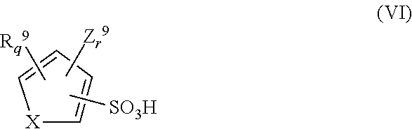
wherein: X is O or S; R9 independently represents a substituted or unsubstituted C1-C20 alkyl group, a substituted or unsubstituted C5-C20 aryl group or a combination thereof, optionally containing one or more group chosen from carbonyl, carbonyloxy, sulfonamido, ether, thioether, a substituted or unsubstituted alkylene group, or a combination thereof; Z9 independently represents a group chosen from carboxyl, hydroxy, nitro, cyano, C1 to C5 alkoxy, formyl and sulfonic acid; q and r are independently an integer from 0 to 3; and q +r is 3 or less.
7. The method of claim 1 , wherein the rising agent comprises water or an aqueous alkaline solution.
8. The method of claim 1 , wherein the rinsing agent comprises an organic solvent or solvent mixture.
9. The method of claim 1 , wherein the aromatic acid is present in the photoresist trimming composition in an amount of from 0.01 to 20 wt % based on total solids of the photoresist trimming composition.
10. The method of claim 9 , wherein the matrix polymer of the photoresist trimming composition is present in the photoresist trimming composition in an amount of from 80 to 99 wt % based on total solids of the photoresist trimming composition.
11. The method of claim 1 , wherein the aromatic acid is a sulfonic acid.
12. The method of claim 11 , wherein the aromatic acid is p-toluenesulfonic acid.
13. The method of claim 11 , wherein the aromatic acid is 2,4-dinitrobenzenesulfonic acid.
14. The method of claim 1 , wherein the photoresist trimming composition is applied to the substrate by spin-coating.
15. The method of claim 1 , wherein a content of the solvent of the photoresist trimming composition is from 90 to 99 wt % based on the trimming composition.
16. The method of claim 1 , wherein the matrix polymer of the photoresist trimming composition is present in the photoresist trimming composition in an amount of from 80 to 99 wt % based on total solids of the photoresist trimming composition.
Priority Applications (1)
| Application Number | Priority Date | Filing Date | Title |
|---|---|---|---|
| US14/145,207 US10162266B2 (en) | 2012-12-31 | 2013-12-31 | Photoresist pattern trimming methods |
Applications Claiming Priority (2)
| Application Number | Priority Date | Filing Date | Title |
|---|---|---|---|
| US201261748035P | 2012-12-31 | 2012-12-31 | |
| US14/145,207 US10162266B2 (en) | 2012-12-31 | 2013-12-31 | Photoresist pattern trimming methods |
Publications (2)
| Publication Number | Publication Date |
|---|---|
| US20140186772A1 US20140186772A1 (en) | 2014-07-03 |
| US10162266B2 true US10162266B2 (en) | 2018-12-25 |
Family
ID=51017569
Family Applications (1)
| Application Number | Title | Priority Date | Filing Date |
|---|---|---|---|
| US14/145,207 Active US10162266B2 (en) | 2012-12-31 | 2013-12-31 | Photoresist pattern trimming methods |
Country Status (5)
| Country | Link |
|---|---|
| US (1) | US10162266B2 (en) |
| JP (1) | JP6328931B2 (en) |
| KR (1) | KR102195470B1 (en) |
| CN (1) | CN103913946B (en) |
| TW (1) | TWI587091B (en) |
Cited By (1)
| Publication number | Priority date | Publication date | Assignee | Title |
|---|---|---|---|---|
| US11003074B2 (en) * | 2017-05-01 | 2021-05-11 | Rohm And Haas Electronic Materials Llc | Pattern formation methods and photoresist pattern overcoat compositions |
Families Citing this family (128)
| Publication number | Priority date | Publication date | Assignee | Title |
|---|---|---|---|---|
| US9324576B2 (en) | 2010-05-27 | 2016-04-26 | Applied Materials, Inc. | Selective etch for silicon films |
| US10283321B2 (en) | 2011-01-18 | 2019-05-07 | Applied Materials, Inc. | Semiconductor processing system and methods using capacitively coupled plasma |
| US9064815B2 (en) | 2011-03-14 | 2015-06-23 | Applied Materials, Inc. | Methods for etch of metal and metal-oxide films |
| US8999856B2 (en) | 2011-03-14 | 2015-04-07 | Applied Materials, Inc. | Methods for etch of sin films |
| US9267739B2 (en) | 2012-07-18 | 2016-02-23 | Applied Materials, Inc. | Pedestal with multi-zone temperature control and multiple purge capabilities |
| US9373517B2 (en) | 2012-08-02 | 2016-06-21 | Applied Materials, Inc. | Semiconductor processing with DC assisted RF power for improved control |
| US9132436B2 (en) | 2012-09-21 | 2015-09-15 | Applied Materials, Inc. | Chemical control features in wafer process equipment |
| JP2014143415A (en) | 2012-12-31 | 2014-08-07 | Rohm & Haas Electronic Materials Llc | Ion implantation method |
| JP6448903B2 (en) | 2012-12-31 | 2019-01-09 | ローム アンド ハース エレクトロニック マテリアルズ エルエルシーRohm and Haas Electronic Materials LLC | Ion implantation method |
| US10256079B2 (en) | 2013-02-08 | 2019-04-09 | Applied Materials, Inc. | Semiconductor processing systems having multiple plasma configurations |
| US9362130B2 (en) | 2013-03-01 | 2016-06-07 | Applied Materials, Inc. | Enhanced etching processes using remote plasma sources |
| US9040422B2 (en) | 2013-03-05 | 2015-05-26 | Applied Materials, Inc. | Selective titanium nitride removal |
| US20140271097A1 (en) | 2013-03-15 | 2014-09-18 | Applied Materials, Inc. | Processing systems and methods for halide scavenging |
| US9493879B2 (en) | 2013-07-12 | 2016-11-15 | Applied Materials, Inc. | Selective sputtering for pattern transfer |
| US9773648B2 (en) | 2013-08-30 | 2017-09-26 | Applied Materials, Inc. | Dual discharge modes operation for remote plasma |
| US9576809B2 (en) | 2013-11-04 | 2017-02-21 | Applied Materials, Inc. | Etch suppression with germanium |
| US9520303B2 (en) | 2013-11-12 | 2016-12-13 | Applied Materials, Inc. | Aluminum selective etch |
| US9245762B2 (en) | 2013-12-02 | 2016-01-26 | Applied Materials, Inc. | Procedure for etch rate consistency |
| CN104749888B (en) | 2013-12-30 | 2019-12-10 | 罗门哈斯电子材料有限公司 | Photoresist pattern trimming compositions and methods |
| US9499898B2 (en) | 2014-03-03 | 2016-11-22 | Applied Materials, Inc. | Layered thin film heater and method of fabrication |
| US9299537B2 (en) | 2014-03-20 | 2016-03-29 | Applied Materials, Inc. | Radial waveguide systems and methods for post-match control of microwaves |
| US9903020B2 (en) | 2014-03-31 | 2018-02-27 | Applied Materials, Inc. | Generation of compact alumina passivation layers on aluminum plasma equipment components |
| US9309598B2 (en) | 2014-05-28 | 2016-04-12 | Applied Materials, Inc. | Oxide and metal removal |
| KR101554103B1 (en) * | 2014-06-10 | 2015-09-17 | 동우 화인켐 주식회사 | Thinner composition for improving coating and removing performance of resist |
| US9425058B2 (en) * | 2014-07-24 | 2016-08-23 | Applied Materials, Inc. | Simplified litho-etch-litho-etch process |
| US9496167B2 (en) | 2014-07-31 | 2016-11-15 | Applied Materials, Inc. | Integrated bit-line airgap formation and gate stack post clean |
| US9659753B2 (en) | 2014-08-07 | 2017-05-23 | Applied Materials, Inc. | Grooved insulator to reduce leakage current |
| US9553102B2 (en) | 2014-08-19 | 2017-01-24 | Applied Materials, Inc. | Tungsten separation |
| WO2016043317A1 (en) | 2014-09-19 | 2016-03-24 | 日産化学工業株式会社 | Application solution for resist pattern coating |
| US9355862B2 (en) | 2014-09-24 | 2016-05-31 | Applied Materials, Inc. | Fluorine-based hardmask removal |
| US9613822B2 (en) | 2014-09-25 | 2017-04-04 | Applied Materials, Inc. | Oxide etch selectivity enhancement |
| TWI675258B (en) * | 2014-09-26 | 2019-10-21 | 日商東京應化工業股份有限公司 | Method for forming resist pattern, resist pattern splitting agent, split pattern improving agent, resist pattern splitting material, and positive resist composition for forming split pattern |
| TWI676863B (en) * | 2014-10-06 | 2019-11-11 | 日商東京應化工業股份有限公司 | Method of trimming resist pattern |
| US9355922B2 (en) | 2014-10-14 | 2016-05-31 | Applied Materials, Inc. | Systems and methods for internal surface conditioning in plasma processing equipment |
| US9966240B2 (en) | 2014-10-14 | 2018-05-08 | Applied Materials, Inc. | Systems and methods for internal surface conditioning assessment in plasma processing equipment |
| KR102480056B1 (en) * | 2014-10-17 | 2022-12-21 | 도오꾜오까고오교 가부시끼가이샤 | Method of forming resist pattern |
| JP6455369B2 (en) * | 2014-10-30 | 2019-01-23 | 信越化学工業株式会社 | Pattern forming method and shrink agent |
| JP6455370B2 (en) * | 2014-10-30 | 2019-01-23 | 信越化学工業株式会社 | Pattern forming method and shrink agent |
| US11637002B2 (en) | 2014-11-26 | 2023-04-25 | Applied Materials, Inc. | Methods and systems to enhance process uniformity |
| US10573496B2 (en) | 2014-12-09 | 2020-02-25 | Applied Materials, Inc. | Direct outlet toroidal plasma source |
| US10224210B2 (en) | 2014-12-09 | 2019-03-05 | Applied Materials, Inc. | Plasma processing system with direct outlet toroidal plasma source |
| US9502258B2 (en) | 2014-12-23 | 2016-11-22 | Applied Materials, Inc. | Anisotropic gap etch |
| TWI617611B (en) * | 2014-12-31 | 2018-03-11 | 羅門哈斯電子材料有限公司 | Photoresist pattern trimming compositions and methods |
| JP6481602B2 (en) * | 2015-01-09 | 2019-03-13 | 信越化学工業株式会社 | Pattern forming method and shrink agent |
| US11257693B2 (en) | 2015-01-09 | 2022-02-22 | Applied Materials, Inc. | Methods and systems to improve pedestal temperature control |
| US20160225652A1 (en) | 2015-02-03 | 2016-08-04 | Applied Materials, Inc. | Low temperature chuck for plasma processing systems |
| US9728437B2 (en) | 2015-02-03 | 2017-08-08 | Applied Materials, Inc. | High temperature chuck for plasma processing systems |
| US9881805B2 (en) | 2015-03-02 | 2018-01-30 | Applied Materials, Inc. | Silicon selective removal |
| JP6503206B2 (en) | 2015-03-19 | 2019-04-17 | 東京応化工業株式会社 | Resist pattern repair method |
| KR102374049B1 (en) | 2015-06-02 | 2022-03-14 | 삼성전자주식회사 | Methods of forming patterns using photoresist |
| US9691645B2 (en) | 2015-08-06 | 2017-06-27 | Applied Materials, Inc. | Bolted wafer chuck thermal management systems and methods for wafer processing systems |
| US9741593B2 (en) | 2015-08-06 | 2017-08-22 | Applied Materials, Inc. | Thermal management systems and methods for wafer processing systems |
| US9349605B1 (en) | 2015-08-07 | 2016-05-24 | Applied Materials, Inc. | Oxide etch selectivity systems and methods |
| US10504700B2 (en) | 2015-08-27 | 2019-12-10 | Applied Materials, Inc. | Plasma etching systems and methods with secondary plasma injection |
| TWI628159B (en) * | 2015-10-31 | 2018-07-01 | 羅門哈斯電子材料有限公司 | Thermal acid generators and photoresist pattern trimming compositions and methods |
| TWI615383B (en) | 2015-10-31 | 2018-02-21 | 羅門哈斯電子材料有限公司 | Thermal acid generators and photoresist pattern trimming compositions and methods |
| US9869933B2 (en) | 2016-03-07 | 2018-01-16 | Rohm And Haas Electronic Materials Llc | Pattern trimming methods |
| US9760011B1 (en) * | 2016-03-07 | 2017-09-12 | Rohm And Haas Electronic Materials Llc | Pattern trimming compositions and methods |
| US11009795B2 (en) * | 2016-03-30 | 2021-05-18 | Nissan Chemical Corporation | Aqueous solution for resist pattern coating and pattern forming methods using the same |
| KR101730838B1 (en) * | 2016-05-04 | 2017-04-28 | 영창케미칼 주식회사 | Process and composition for improving line width roughness of nega tone photoresist pattern |
| US10522371B2 (en) | 2016-05-19 | 2019-12-31 | Applied Materials, Inc. | Systems and methods for improved semiconductor etching and component protection |
| US10504754B2 (en) | 2016-05-19 | 2019-12-10 | Applied Materials, Inc. | Systems and methods for improved semiconductor etching and component protection |
| US9865484B1 (en) | 2016-06-29 | 2018-01-09 | Applied Materials, Inc. | Selective etch using material modification and RF pulsing |
| US10629473B2 (en) | 2016-09-09 | 2020-04-21 | Applied Materials, Inc. | Footing removal for nitride spacer |
| US10062575B2 (en) | 2016-09-09 | 2018-08-28 | Applied Materials, Inc. | Poly directional etch by oxidation |
| US9721789B1 (en) | 2016-10-04 | 2017-08-01 | Applied Materials, Inc. | Saving ion-damaged spacers |
| US9934942B1 (en) | 2016-10-04 | 2018-04-03 | Applied Materials, Inc. | Chamber with flow-through source |
| US10062585B2 (en) | 2016-10-04 | 2018-08-28 | Applied Materials, Inc. | Oxygen compatible plasma source |
| US10546729B2 (en) | 2016-10-04 | 2020-01-28 | Applied Materials, Inc. | Dual-channel showerhead with improved profile |
| US10062579B2 (en) | 2016-10-07 | 2018-08-28 | Applied Materials, Inc. | Selective SiN lateral recess |
| US9947549B1 (en) | 2016-10-10 | 2018-04-17 | Applied Materials, Inc. | Cobalt-containing material removal |
| US9768034B1 (en) | 2016-11-11 | 2017-09-19 | Applied Materials, Inc. | Removal methods for high aspect ratio structures |
| US10163696B2 (en) | 2016-11-11 | 2018-12-25 | Applied Materials, Inc. | Selective cobalt removal for bottom up gapfill |
| US10242908B2 (en) | 2016-11-14 | 2019-03-26 | Applied Materials, Inc. | Airgap formation with damage-free copper |
| US10026621B2 (en) | 2016-11-14 | 2018-07-17 | Applied Materials, Inc. | SiN spacer profile patterning |
| US10566206B2 (en) | 2016-12-27 | 2020-02-18 | Applied Materials, Inc. | Systems and methods for anisotropic material breakthrough |
| US10684549B2 (en) * | 2016-12-31 | 2020-06-16 | Rohm And Haas Electronic Materials Llc | Pattern-formation methods |
| US10431429B2 (en) | 2017-02-03 | 2019-10-01 | Applied Materials, Inc. | Systems and methods for radial and azimuthal control of plasma uniformity |
| US10403507B2 (en) | 2017-02-03 | 2019-09-03 | Applied Materials, Inc. | Shaped etch profile with oxidation |
| US10043684B1 (en) | 2017-02-06 | 2018-08-07 | Applied Materials, Inc. | Self-limiting atomic thermal etching systems and methods |
| US10319739B2 (en) | 2017-02-08 | 2019-06-11 | Applied Materials, Inc. | Accommodating imperfectly aligned memory holes |
| US10943834B2 (en) | 2017-03-13 | 2021-03-09 | Applied Materials, Inc. | Replacement contact process |
| US10319649B2 (en) | 2017-04-11 | 2019-06-11 | Applied Materials, Inc. | Optical emission spectroscopy (OES) for remote plasma monitoring |
| CN107146796B (en) * | 2017-04-13 | 2019-12-31 | 武汉新芯集成电路制造有限公司 | Method for improving resolution of back metal grid and semiconductor structure |
| US11276590B2 (en) | 2017-05-17 | 2022-03-15 | Applied Materials, Inc. | Multi-zone semiconductor substrate supports |
| US11276559B2 (en) | 2017-05-17 | 2022-03-15 | Applied Materials, Inc. | Semiconductor processing chamber for multiple precursor flow |
| US10497579B2 (en) | 2017-05-31 | 2019-12-03 | Applied Materials, Inc. | Water-free etching methods |
| US10049891B1 (en) | 2017-05-31 | 2018-08-14 | Applied Materials, Inc. | Selective in situ cobalt residue removal |
| US10920320B2 (en) | 2017-06-16 | 2021-02-16 | Applied Materials, Inc. | Plasma health determination in semiconductor substrate processing reactors |
| US10541246B2 (en) | 2017-06-26 | 2020-01-21 | Applied Materials, Inc. | 3D flash memory cells which discourage cross-cell electrical tunneling |
| US10727080B2 (en) | 2017-07-07 | 2020-07-28 | Applied Materials, Inc. | Tantalum-containing material removal |
| US10541184B2 (en) | 2017-07-11 | 2020-01-21 | Applied Materials, Inc. | Optical emission spectroscopic techniques for monitoring etching |
| US10354889B2 (en) | 2017-07-17 | 2019-07-16 | Applied Materials, Inc. | Non-halogen etching of silicon-containing materials |
| US10043674B1 (en) | 2017-08-04 | 2018-08-07 | Applied Materials, Inc. | Germanium etching systems and methods |
| US10170336B1 (en) | 2017-08-04 | 2019-01-01 | Applied Materials, Inc. | Methods for anisotropic control of selective silicon removal |
| US10297458B2 (en) | 2017-08-07 | 2019-05-21 | Applied Materials, Inc. | Process window widening using coated parts in plasma etch processes |
| US10691023B2 (en) * | 2017-08-24 | 2020-06-23 | Taiwan Semiconductor Manufacturing Co., Ltd. | Method for performing lithography process with post treatment |
| US10283324B1 (en) | 2017-10-24 | 2019-05-07 | Applied Materials, Inc. | Oxygen treatment for nitride etching |
| US10128086B1 (en) | 2017-10-24 | 2018-11-13 | Applied Materials, Inc. | Silicon pretreatment for nitride removal |
| US10256112B1 (en) | 2017-12-08 | 2019-04-09 | Applied Materials, Inc. | Selective tungsten removal |
| US10903054B2 (en) | 2017-12-19 | 2021-01-26 | Applied Materials, Inc. | Multi-zone gas distribution systems and methods |
| US11328909B2 (en) | 2017-12-22 | 2022-05-10 | Applied Materials, Inc. | Chamber conditioning and removal processes |
| US10854426B2 (en) | 2018-01-08 | 2020-12-01 | Applied Materials, Inc. | Metal recess for semiconductor structures |
| US10679870B2 (en) | 2018-02-15 | 2020-06-09 | Applied Materials, Inc. | Semiconductor processing chamber multistage mixing apparatus |
| US10964512B2 (en) | 2018-02-15 | 2021-03-30 | Applied Materials, Inc. | Semiconductor processing chamber multistage mixing apparatus and methods |
| TWI716818B (en) | 2018-02-28 | 2021-01-21 | 美商應用材料股份有限公司 | Systems and methods to form airgaps |
| US10593560B2 (en) | 2018-03-01 | 2020-03-17 | Applied Materials, Inc. | Magnetic induction plasma source for semiconductor processes and equipment |
| US10319600B1 (en) | 2018-03-12 | 2019-06-11 | Applied Materials, Inc. | Thermal silicon etch |
| US10497573B2 (en) | 2018-03-13 | 2019-12-03 | Applied Materials, Inc. | Selective atomic layer etching of semiconductor materials |
| US10573527B2 (en) | 2018-04-06 | 2020-02-25 | Applied Materials, Inc. | Gas-phase selective etching systems and methods |
| US10490406B2 (en) | 2018-04-10 | 2019-11-26 | Appled Materials, Inc. | Systems and methods for material breakthrough |
| US10699879B2 (en) | 2018-04-17 | 2020-06-30 | Applied Materials, Inc. | Two piece electrode assembly with gap for plasma control |
| US10886137B2 (en) | 2018-04-30 | 2021-01-05 | Applied Materials, Inc. | Selective nitride removal |
| US10872778B2 (en) | 2018-07-06 | 2020-12-22 | Applied Materials, Inc. | Systems and methods utilizing solid-phase etchants |
| US10755941B2 (en) | 2018-07-06 | 2020-08-25 | Applied Materials, Inc. | Self-limiting selective etching systems and methods |
| US10672642B2 (en) | 2018-07-24 | 2020-06-02 | Applied Materials, Inc. | Systems and methods for pedestal configuration |
| US10892198B2 (en) | 2018-09-14 | 2021-01-12 | Applied Materials, Inc. | Systems and methods for improved performance in semiconductor processing |
| US11049755B2 (en) | 2018-09-14 | 2021-06-29 | Applied Materials, Inc. | Semiconductor substrate supports with embedded RF shield |
| US11062887B2 (en) | 2018-09-17 | 2021-07-13 | Applied Materials, Inc. | High temperature RF heater pedestals |
| US11417534B2 (en) | 2018-09-21 | 2022-08-16 | Applied Materials, Inc. | Selective material removal |
| US11682560B2 (en) | 2018-10-11 | 2023-06-20 | Applied Materials, Inc. | Systems and methods for hafnium-containing film removal |
| US11121002B2 (en) | 2018-10-24 | 2021-09-14 | Applied Materials, Inc. | Systems and methods for etching metals and metal derivatives |
| US11437242B2 (en) | 2018-11-27 | 2022-09-06 | Applied Materials, Inc. | Selective removal of silicon-containing materials |
| US11721527B2 (en) | 2019-01-07 | 2023-08-08 | Applied Materials, Inc. | Processing chamber mixing systems |
| US10920319B2 (en) | 2019-01-11 | 2021-02-16 | Applied Materials, Inc. | Ceramic showerheads with conductive electrodes |
| US11506981B2 (en) | 2019-05-31 | 2022-11-22 | Rohm And Haas Electronic Materials Llc | Photoresist pattern trimming compositions and pattern formation methods |
| US11754927B2 (en) | 2019-05-31 | 2023-09-12 | Rohm And Haas Electronic Materials Llc | Photoresist pattern trimming compositions and pattern formation methods |
| WO2021055542A1 (en) | 2019-09-19 | 2021-03-25 | Tokyo Electron Limited | Method of forming a narrow trench |
Citations (26)
| Publication number | Priority date | Publication date | Assignee | Title |
|---|---|---|---|---|
| US4511683A (en) * | 1982-03-08 | 1985-04-16 | Japan Synthetic Rubber Co., Ltd. | Sulfonic acid compound having cyclopentadiene skeleton and composition comprising same and cement |
| US5247116A (en) * | 1992-07-10 | 1993-09-21 | Temple University Of The Commonwealth System Of Higher Education | Acid-catalyzed process for the production of cyclosiloxanes |
| US6180320B1 (en) | 1998-03-09 | 2001-01-30 | Mitsubishi Denki Kabushiki Kaisha | Method of manufacturing a semiconductor device having a fine pattern, and semiconductor device manufactured thereby |
| US6274289B1 (en) | 2000-06-16 | 2001-08-14 | Advanced Micro Devices, Inc. | Chemical resist thickness reduction process |
| JP2002006512A (en) | 2000-06-20 | 2002-01-09 | Mitsubishi Electric Corp | Fine pattern forming method, fine pattern forming material and method for producing semiconductor device using the method |
| US6372829B1 (en) | 1999-10-06 | 2002-04-16 | 3M Innovative Properties Company | Antistatic composition |
| JP2002299202A (en) | 2001-03-29 | 2002-10-11 | Sony Corp | Method for fabricating semiconductor device |
| US6492075B1 (en) | 2000-06-16 | 2002-12-10 | Advanced Micro Devices, Inc. | Chemical trim process |
| US20030138736A1 (en) * | 2000-02-04 | 2003-07-24 | Kazuyuki Nitta | Method for decreasing surface defects of patterned resist layer |
| US20040142279A1 (en) | 2002-12-30 | 2004-07-22 | Bok Cheol Kyu | Overcoating composition for photoresist and method for forming photoresist pattern using the same |
| US20060263728A1 (en) | 2001-11-05 | 2006-11-23 | Hiroshi Shinbori | Method of forming fine patterns |
| US7338750B2 (en) | 2002-01-25 | 2008-03-04 | Fujitsu Limited | Resist pattern thickness reducing material, resist pattern and process for forming thereof, and semiconductor device and process for manufacturing thereof |
| US20080063985A1 (en) | 2006-09-12 | 2008-03-13 | Hynix Semiconductor Inc. | Method for forming fine pattern of semiconductor device |
| JP4329216B2 (en) | 2000-03-31 | 2009-09-09 | Jsr株式会社 | Resist pattern reduction material and method for forming fine resist pattern using the same |
| CN101592858A (en) | 2008-05-30 | 2009-12-02 | 中芯国际集成电路制造(北京)有限公司 | Revise the method for photoresist pattern error |
| JP2010049247A (en) | 2008-07-24 | 2010-03-04 | Jsr Corp | Composition for resist pattern microfabrication, and method for forming resist pattern |
| US7862982B2 (en) * | 2008-06-12 | 2011-01-04 | International Business Machines Corporation | Chemical trim of photoresist lines by means of a tuned overcoat material |
| US20110174774A1 (en) | 2010-01-21 | 2011-07-21 | Ying-Chih Lin | Method of descumming patterned photoresist |
| US8067148B2 (en) | 2009-02-27 | 2011-11-29 | Panasonic Corporation | Pattern forming method |
| CN102376561A (en) | 2010-08-18 | 2012-03-14 | 中芯国际集成电路制造(上海)有限公司 | Etching method |
| US20120219919A1 (en) * | 2011-02-24 | 2012-08-30 | Muthiah Thiyagarajan | Composition for Coating over a Photoresist Pattern Comprising a Lactam |
| US20130171825A1 (en) * | 2011-12-31 | 2013-07-04 | Rohm And Haas Electronic Materials Llc | Photoresist pattern trimming methods |
| US20130171574A1 (en) | 2011-12-31 | 2013-07-04 | Rohm And Haas Electronic Materials Llc | Photoresist pattern trimming methods |
| US20140187027A1 (en) | 2012-12-31 | 2014-07-03 | Rohm And Haas Electronic Materials Llc | Ion implantation methods |
| US20150214056A1 (en) | 2012-12-31 | 2015-07-30 | Rohm And Haas Electronic Materials Llc | Ion implantation methods |
| US9448486B2 (en) * | 2013-12-30 | 2016-09-20 | Rohm And Haas Electronic Materials Llc | Photoresist pattern trimming compositions and methods |
Family Cites Families (3)
| Publication number | Priority date | Publication date | Assignee | Title |
|---|---|---|---|---|
| JP5306755B2 (en) * | 2008-09-16 | 2013-10-02 | AzエレクトロニックマテリアルズIp株式会社 | Substrate processing liquid and resist substrate processing method using the same |
| US20100297851A1 (en) * | 2009-05-19 | 2010-11-25 | Rohm And Haas Electronic Materials Llc | Compositions and methods for multiple exposure photolithography |
| JP2012032757A (en) * | 2010-07-06 | 2012-02-16 | Tosoh Corp | Resist stripping agent and stripping method using the same |
-
2013
- 2013-12-27 JP JP2013273120A patent/JP6328931B2/en active Active
- 2013-12-30 TW TW102148976A patent/TWI587091B/en active
- 2013-12-31 US US14/145,207 patent/US10162266B2/en active Active
- 2013-12-31 KR KR1020130168104A patent/KR102195470B1/en active IP Right Grant
- 2013-12-31 CN CN201310757477.XA patent/CN103913946B/en active Active
Patent Citations (26)
| Publication number | Priority date | Publication date | Assignee | Title |
|---|---|---|---|---|
| US4511683A (en) * | 1982-03-08 | 1985-04-16 | Japan Synthetic Rubber Co., Ltd. | Sulfonic acid compound having cyclopentadiene skeleton and composition comprising same and cement |
| US5247116A (en) * | 1992-07-10 | 1993-09-21 | Temple University Of The Commonwealth System Of Higher Education | Acid-catalyzed process for the production of cyclosiloxanes |
| US6180320B1 (en) | 1998-03-09 | 2001-01-30 | Mitsubishi Denki Kabushiki Kaisha | Method of manufacturing a semiconductor device having a fine pattern, and semiconductor device manufactured thereby |
| US6372829B1 (en) | 1999-10-06 | 2002-04-16 | 3M Innovative Properties Company | Antistatic composition |
| US20030138736A1 (en) * | 2000-02-04 | 2003-07-24 | Kazuyuki Nitta | Method for decreasing surface defects of patterned resist layer |
| JP4329216B2 (en) | 2000-03-31 | 2009-09-09 | Jsr株式会社 | Resist pattern reduction material and method for forming fine resist pattern using the same |
| US6274289B1 (en) | 2000-06-16 | 2001-08-14 | Advanced Micro Devices, Inc. | Chemical resist thickness reduction process |
| US6492075B1 (en) | 2000-06-16 | 2002-12-10 | Advanced Micro Devices, Inc. | Chemical trim process |
| JP2002006512A (en) | 2000-06-20 | 2002-01-09 | Mitsubishi Electric Corp | Fine pattern forming method, fine pattern forming material and method for producing semiconductor device using the method |
| JP2002299202A (en) | 2001-03-29 | 2002-10-11 | Sony Corp | Method for fabricating semiconductor device |
| US20060263728A1 (en) | 2001-11-05 | 2006-11-23 | Hiroshi Shinbori | Method of forming fine patterns |
| US7338750B2 (en) | 2002-01-25 | 2008-03-04 | Fujitsu Limited | Resist pattern thickness reducing material, resist pattern and process for forming thereof, and semiconductor device and process for manufacturing thereof |
| US20040142279A1 (en) | 2002-12-30 | 2004-07-22 | Bok Cheol Kyu | Overcoating composition for photoresist and method for forming photoresist pattern using the same |
| US20080063985A1 (en) | 2006-09-12 | 2008-03-13 | Hynix Semiconductor Inc. | Method for forming fine pattern of semiconductor device |
| CN101592858A (en) | 2008-05-30 | 2009-12-02 | 中芯国际集成电路制造(北京)有限公司 | Revise the method for photoresist pattern error |
| US7862982B2 (en) * | 2008-06-12 | 2011-01-04 | International Business Machines Corporation | Chemical trim of photoresist lines by means of a tuned overcoat material |
| JP2010049247A (en) | 2008-07-24 | 2010-03-04 | Jsr Corp | Composition for resist pattern microfabrication, and method for forming resist pattern |
| US8067148B2 (en) | 2009-02-27 | 2011-11-29 | Panasonic Corporation | Pattern forming method |
| US20110174774A1 (en) | 2010-01-21 | 2011-07-21 | Ying-Chih Lin | Method of descumming patterned photoresist |
| CN102376561A (en) | 2010-08-18 | 2012-03-14 | 中芯国际集成电路制造(上海)有限公司 | Etching method |
| US20120219919A1 (en) * | 2011-02-24 | 2012-08-30 | Muthiah Thiyagarajan | Composition for Coating over a Photoresist Pattern Comprising a Lactam |
| US20130171825A1 (en) * | 2011-12-31 | 2013-07-04 | Rohm And Haas Electronic Materials Llc | Photoresist pattern trimming methods |
| US20130171574A1 (en) | 2011-12-31 | 2013-07-04 | Rohm And Haas Electronic Materials Llc | Photoresist pattern trimming methods |
| US20140187027A1 (en) | 2012-12-31 | 2014-07-03 | Rohm And Haas Electronic Materials Llc | Ion implantation methods |
| US20150214056A1 (en) | 2012-12-31 | 2015-07-30 | Rohm And Haas Electronic Materials Llc | Ion implantation methods |
| US9448486B2 (en) * | 2013-12-30 | 2016-09-20 | Rohm And Haas Electronic Materials Llc | Photoresist pattern trimming compositions and methods |
Non-Patent Citations (3)
| Title |
|---|
| Search report for corresponding China Application No. 201310757477.X dated Jun. 14, 2018. |
| Search report for corresponding Chinese Application No. 201310757477.X dated Jun. 17, 2016. |
| Search Report for corresponding Taiwanese Application No. 102148976, dated Feb. 9, 2015. |
Cited By (2)
| Publication number | Priority date | Publication date | Assignee | Title |
|---|---|---|---|---|
| US11003074B2 (en) * | 2017-05-01 | 2021-05-11 | Rohm And Haas Electronic Materials Llc | Pattern formation methods and photoresist pattern overcoat compositions |
| US11796916B2 (en) | 2017-05-01 | 2023-10-24 | Rohm And Haas Electronic Materials Llc | Pattern formation methods and photoresist pattern overcoat compositions |
Also Published As
| Publication number | Publication date |
|---|---|
| US20140186772A1 (en) | 2014-07-03 |
| JP2014142634A (en) | 2014-08-07 |
| JP6328931B2 (en) | 2018-05-23 |
| CN103913946A (en) | 2014-07-09 |
| KR102195470B1 (en) | 2020-12-28 |
| KR20140088033A (en) | 2014-07-09 |
| TW201441768A (en) | 2014-11-01 |
| CN103913946B (en) | 2019-04-16 |
| TWI587091B (en) | 2017-06-11 |
Similar Documents
| Publication | Publication Date | Title |
|---|---|---|
| US10162266B2 (en) | Photoresist pattern trimming methods | |
| US9996008B2 (en) | Photoresist pattern trimming methods | |
| US9583344B2 (en) | Photoresist pattern trimming methods | |
| US9448486B2 (en) | Photoresist pattern trimming compositions and methods | |
| US9209028B2 (en) | Ion implantation methods | |
| US9696629B2 (en) | Photoresist pattern trimming compositions and methods | |
| US9869933B2 (en) | Pattern trimming methods | |
| TWI556290B (en) | Ion implantation methods | |
| US10684549B2 (en) | Pattern-formation methods | |
| US9760011B1 (en) | Pattern trimming compositions and methods |
Legal Events
| Date | Code | Title | Description |
|---|---|---|---|
| AS | Assignment |
Owner name: ROHM AND HAAS ELECTRONIC MATERIALS LLC, MASSACHUSE Free format text: ASSIGNMENT OF ASSIGNORS INTEREST;ASSIGNORS:POHLERS, GERHARD;XU, CHENG-BAI;ROWELL, KEVIN;SIGNING DATES FROM 20140204 TO 20140206;REEL/FRAME:036519/0803 |
|
| STCF | Information on status: patent grant |
Free format text: PATENTED CASE |
|
| MAFP | Maintenance fee payment |
Free format text: PAYMENT OF MAINTENANCE FEE, 4TH YEAR, LARGE ENTITY (ORIGINAL EVENT CODE: M1551); ENTITY STATUS OF PATENT OWNER: LARGE ENTITY Year of fee payment: 4 |