US10151972B2 - Manufacturing method of photomask and recording medium - Google Patents
Manufacturing method of photomask and recording medium Download PDFInfo
- Publication number
- US10151972B2 US10151972B2 US15/446,544 US201715446544A US10151972B2 US 10151972 B2 US10151972 B2 US 10151972B2 US 201715446544 A US201715446544 A US 201715446544A US 10151972 B2 US10151972 B2 US 10151972B2
- Authority
- US
- United States
- Prior art keywords
- target shape
- shape
- pattern
- resist
- cost function
- Prior art date
- Legal status (The legal status is an assumption and is not a legal conclusion. Google has not performed a legal analysis and makes no representation as to the accuracy of the status listed.)
- Active, expires
Links
Images


Classifications
-
- G—PHYSICS
- G03—PHOTOGRAPHY; CINEMATOGRAPHY; ANALOGOUS TECHNIQUES USING WAVES OTHER THAN OPTICAL WAVES; ELECTROGRAPHY; HOLOGRAPHY
- G03F—PHOTOMECHANICAL PRODUCTION OF TEXTURED OR PATTERNED SURFACES, e.g. FOR PRINTING, FOR PROCESSING OF SEMICONDUCTOR DEVICES; MATERIALS THEREFOR; ORIGINALS THEREFOR; APPARATUS SPECIALLY ADAPTED THEREFOR
- G03F1/00—Originals for photomechanical production of textured or patterned surfaces, e.g., masks, photo-masks, reticles; Mask blanks or pellicles therefor; Containers specially adapted therefor; Preparation thereof
- G03F1/68—Preparation processes not covered by groups G03F1/20 - G03F1/50
- G03F1/70—Adapting basic layout or design of masks to lithographic process requirements, e.g., second iteration correction of mask patterns for imaging
Definitions
- Embodiments of the present invention relate to a manufacturing method of a photomask, and a recording medium.
- a resist is fabricated into a three-dimensional shape by using a photomask in some cases.
- a pattern of the photomask is set based on, for example, thickness data of a resist remaining for an exposure amount.
- FIG. 1 is a flowchart showing steps of manufacturing a photomask according to a first embodiment.
- FIG. 2 is a diagram showing exemplary thickness data of a resist according to the first embodiment.
- FIG. 3 is a diagram showing an exemplary target shape of the resist according to the first embodiment.
- FIG. 4 is a diagram showing an exemplary hypothetical target shape of the resist according to the first embodiment.
- FIG. 5 is a plan view showing an exemplary pattern of the photomask according to the first embodiment.
- FIG. 6 is a diagram for description of an edge placement error.
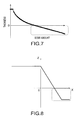
- FIG. 7 is a diagram showing exemplary thickness data of a resist according to a second embodiment.
- FIG. 8 is a diagram showing an exemplary hypothetical target shape of the resist according to the second embodiment.
- FIG. 9 is a diagram showing an exemplary pattern of a photomask according to the second embodiment.
- FIG. 10 is a diagram showing an exemplary target shape of a resist according to a third embodiment.
- FIG. 11 is a diagram showing an exemplary prediction shape of the resist according to the third embodiment.
- a manufacturing method of a photomask sets an exposure condition applied when a resist is formed into a three-dimensional target shape by using a photomask including a plurality of light-shielding areas. Subsequently, the method sets a hypothetical target shape obtained by correcting the target shape based on a development characteristic of the resist for the exposure condition. Subsequently, the method creates a pattern of the photomask corresponding to the hypothetical target shape. Subsequently, the method simulates a prediction shape of the resist when the pattern is used. Subsequently, the method calculates a cost function related to an error between the prediction shape and the hypothetical target shape. Subsequently, the method adjusts the pattern based on a result of the calculation of the cost function.
- FIG. 1 is a flowchart showing steps of manufacturing a photomask according to a first embodiment. These manufacturing steps can be recorded, for example, in a non-transitory recording medium as a computer-readable program.
- This computer can be included in, for example, a simulation apparatus to predict the shape of a resist based on a pattern of a photomask or the like.
- a simulation condition is a setting condition of a physicochemical model reflecting a physicochemical characteristic of the resist against, for example, heat and acid.
- the thickness data indicates the thickness of a resist film remaining for a dose amount (exposure amount) as shown in FIG. 2 . In the embodiment, the thickness of the resist film decreases as the dose amount increases.
- the shape data of the resist indicates a target shape actually formed by using a photomask.
- FIG. 3 shows the target shape with two-dimensional coordinate axes.
- the actual shape data is three-dimensional data represented with three-dimensional coordinate axes.
- an exposure condition applied when the target shape is formed is set based on the above-described thickness data and shape data (step S 12 ).
- This exposure condition includes at least one of, for example, an exposure wavelength, the numerical aperture (NA) of a projection lens, an exposure amount, a focus value, the transmissivity of a photomask, and the luminance distribution of a light source.
- NA numerical aperture
- a hypothetical target shape is set (step S 13 ).
- the hypothetical target shape is obtained by correcting the target shape based on a development characteristic of the resist for the above-described exposure condition.
- the development characteristic of the resist includes physicochemical characteristics in the horizontal direction, such as blurring of an optical image and acid diffusion.
- the resist is fabricated into a shape as shown with the dashed and single-dotted line in FIG. 4 due to the development characteristic of the resist in the horizontal direction in some cases. In such a case, a shape error from a target shape shown with the dotted line occurs at a lower end part of the resist.
- a hypothetical target shape with the development characteristic of the resist taken into account in advance is set as shown with the solid line in FIG. 4 .
- Development characteristic data for setting the hypothetical target shape may be input together with any other data at step S 11 or may be stored in the simulation apparatus in advance.
- FIG. 5 is a plan view showing an exemplary pattern of the photomask.
- a photomask 1 shown in FIG. 5 includes a plurality of light-shielding areas 11 arranged in a dotted pattern. Each light-shielding area 11 has a property of transmitting light from a light source to some extent instead of completely shielding the light.
- a transmissivity t of the light-shielding area 11 necessary for forming the hypothetical target shape is firstly calculated (step S 14 ).
- the transmissivity t is calculated by using Expression (1) below.
- “Do” means the intensity of incident light on the light-shielding area 11
- “De” means the intensity of transmitted light from the light-shielding area 11 .
- t De/Do (1)
- a size w of each light-shielding area 11 is calculated based on the above-described distribution of the transmissivity (step S 15 ).
- the size w is calculated by using Expression (2) below.
- P means a pitch between the light-shielding areas 11 .
- w P (1 ⁇ ⁇ square root over (t) ⁇ ) (2)
- step S 16 pattern data of the photomask is created.
- step S 17 a prediction shape of the resist using the above-described pattern data is simulated. Then, the shape of the resist is predicted based on the simulation condition input at step S 11 .
- the simulation is preferably performed under another exposure condition with a different exposure amount as well as the exposure condition set at step S 12 .
- the shape of the resist when the exposure amount has fluctuations can be predicted by performing the simulation a plurality of times.
- a cost function related to an error between the prediction shape and the hypothetical target shape is calculated (step S 18 ).
- the cost function is calculated by using Expression (3) below.
- EPE means a positional shift in the horizontal direction between an edge of the prediction shape and an edge of the hypothetical target shape as shown in FIG. 6 , which is called an edge placement error.
- the root mean square (RMS) of the edge placement error is used as the cost function.
- the cost function calculates the sum of the root mean square of the edge placement error corresponding to each exposure condition.
- step S 19 whether a calculated value of the cost function meets a termination condition for the pattern adjustment of the photomask is determined. For example, the pattern adjustment of the photomask is terminated if the calculated value of the cost function is equal to or less than a threshold, or if the number of times of calculation of the cost function reaches a predetermined number of times.
- a numerical value optimization algorithm that minimizes the error between the hypothetical target shape and the prediction shape, in other words, a value calculated through the above-described Expression (3), is used to set the exposure condition again and change at least one of the size and position of each light-shielding area 11 .
- a numerical value optimization algorithm that minimizes the error between the hypothetical target shape and the prediction shape, in other words, a value calculated through the above-described Expression (3), is used to set the exposure condition again and change at least one of the size and position of each light-shielding area 11 .
- an optimum pattern of the photomask is derived. Accordingly, an error between the shape of a resist formed by using this pattern of the photomask and the target shape (refer to FIG. 3 ) becomes extremely small.
- the hypothetical target shape with the development characteristic of the resist in the horizontal direction taken into account is set so as to adjust an optimum pattern of the photomask for the hypothetical target shape.
- the adjusted pattern of the photomask is used to fabricate the resist, an error from the target shape can be improved.
- the pattern of the photomask is optimized through the cost function that takes into account the EPE of each exposure condition. Accordingly, influence of fluctuation in the exposure amount on the actual shape of the resist can be minimized.
- Steps of manufacturing a photomask according to a second embodiment will be described with focus on any difference from those of the first embodiment.
- the dose amount is set up to the thickness of the resist being zero, as shown in FIG. 2 .
- the thickness data no pattern of the photomask exists in an area outside of the resist film.
- the thickness data of the resist includes hypothetically negative thickness data as shown in the dotted-line region in FIG. 7 .
- the dose amount corresponding to the negative thickness data is larger than the dose amount when the thickness is zero.
- a pattern of a photomask 2 as shown in FIG. 9 is created based on the hypothetical target shape shown in FIG. 8 .
- An auxiliary pattern 20 corresponding to a part having the above-described negative thickness is created at an end part of the photomask 2 .
- the auxiliary pattern 20 includes a plurality of light-shielding areas 21 .
- a pattern of a photomask is created through steps similarly to those of the first embodiment shown in FIG. 1 .
- the target shape of the resist is a stair-shaped as shown in FIG. 10 .
- the hypothetical target shape (not shown) set at step S 13 is a stair-shaped obtained by correcting the target shape based on the development characteristic of the resist in the horizontal direction.
- the EPE and an angle difference between the prediction shape and the hypothetical target shape have a trade-off relation.
- the units of the EPE and the angle are different from each other.
- this relation is expressed by using a weighting coefficient w 1 (first weighting coefficient) and a weighting coefficient w 2 (second weighting coefficient) as in Expression (4).
- the cost function adds a shape error obtained by multiplying the RMS of the EPE with the weighting coefficient w 1 , to an angle error obtained by multiplying, with the weighting coefficient w 2 , the sum of the RMS of an angle difference between the prediction shape and the hypothetical target shape at each step.
- step S 18 when the sum of the shape error and the angle error does not meet the termination condition of the pattern adjustment, the exposure condition and each light-shielding area 11 are adjusted again by using a numerical value optimization algorithm that minimizes this sum. As a result, an optimum pattern of the photomask for forming the resist into the stair-shaped is derived.
- the cost function includes the angle error of each step in addition to the shape error of the EPE. Then, the pattern of the photomask is adjusted to minimize these two errors. Accordingly, the stair-shaped of the resist can be highly accurately controlled.
- the pattern of the photomask is optimized through the cost function that takes into account the shape error and the angle error of each exposure condition. Accordingly, influence of fluctuation in, for example, the exposure amount on the stair-shaped of the resist can be minimized.
- the manufacturing method of a photomask according to the embodiment can achieve reduced fluctuation in size and angle.
Landscapes
- Physics & Mathematics (AREA)
- General Physics & Mathematics (AREA)
- Preparing Plates And Mask In Photomechanical Process (AREA)
- Exposure And Positioning Against Photoresist Photosensitive Materials (AREA)
Abstract
Description
t=De/Do (1)
w=P(1−√{square root over (t)}) (2)
Claims (10)
Priority Applications (1)
| Application Number | Priority Date | Filing Date | Title |
|---|---|---|---|
| US15/446,544 US10151972B2 (en) | 2016-12-06 | 2017-03-01 | Manufacturing method of photomask and recording medium |
Applications Claiming Priority (2)
| Application Number | Priority Date | Filing Date | Title |
|---|---|---|---|
| US201662430381P | 2016-12-06 | 2016-12-06 | |
| US15/446,544 US10151972B2 (en) | 2016-12-06 | 2017-03-01 | Manufacturing method of photomask and recording medium |
Publications (2)
| Publication Number | Publication Date |
|---|---|
| US20180157167A1 US20180157167A1 (en) | 2018-06-07 |
| US10151972B2 true US10151972B2 (en) | 2018-12-11 |
Family
ID=62240045
Family Applications (1)
| Application Number | Title | Priority Date | Filing Date |
|---|---|---|---|
| US15/446,544 Active 2037-07-13 US10151972B2 (en) | 2016-12-06 | 2017-03-01 | Manufacturing method of photomask and recording medium |
Country Status (1)
| Country | Link |
|---|---|
| US (1) | US10151972B2 (en) |
Cited By (2)
| Publication number | Priority date | Publication date | Assignee | Title |
|---|---|---|---|---|
| TWI804920B (en) * | 2020-07-16 | 2023-06-11 | 德商卡爾蔡司Smt有限公司 | Method, device and computer program for repairing a mask for lithography |
| US20250155797A1 (en) * | 2021-12-16 | 2025-05-15 | Applied Materials, Inc. | Generate 3d photoresist profiles using digital lithography |
Families Citing this family (2)
| Publication number | Priority date | Publication date | Assignee | Title |
|---|---|---|---|---|
| CN110189241B (en) * | 2019-04-26 | 2023-01-31 | 江苏水印科技有限公司 | Block mean value-based anti-printing noise image watermarking method |
| US20220284344A1 (en) * | 2019-08-13 | 2022-09-08 | Asml Netherlands B.V. | Method for training machine learning model for improving patterning process |
Citations (6)
| Publication number | Priority date | Publication date | Assignee | Title |
|---|---|---|---|---|
| JP2004047755A (en) | 2002-07-12 | 2004-02-12 | Renesas Technology Corp | Exposure condition determination system |
| US20050130045A1 (en) | 2003-01-28 | 2005-06-16 | Ken Ozawa | Exposing mask and production method therefor and exposing method |
| JP2010267570A (en) | 2009-05-18 | 2010-11-25 | Yokogawa Electric Corp | Characteristic analyzer |
| JP5077656B2 (en) | 2007-06-18 | 2012-11-21 | 株式会社ニコン | Pattern data processing method and system, and exposure method and apparatus |
| JP5673947B2 (en) | 2011-03-01 | 2015-02-18 | 大日本印刷株式会社 | Mask pattern correction method, program, and photomask using the correction method |
| US20160268278A1 (en) | 2015-03-12 | 2016-09-15 | Kabushiki Kaisha Toshiba | Microstructure device and method for manufacturing the same |
-
2017
- 2017-03-01 US US15/446,544 patent/US10151972B2/en active Active
Patent Citations (8)
| Publication number | Priority date | Publication date | Assignee | Title |
|---|---|---|---|---|
| JP2004047755A (en) | 2002-07-12 | 2004-02-12 | Renesas Technology Corp | Exposure condition determination system |
| US6801297B2 (en) | 2002-07-12 | 2004-10-05 | Renesas Technology Corp. | Exposure condition determination system |
| US20050130045A1 (en) | 2003-01-28 | 2005-06-16 | Ken Ozawa | Exposing mask and production method therefor and exposing method |
| JP2005165248A (en) | 2003-01-28 | 2005-06-23 | Sony Corp | Exposure mask, method of manufacturing the same, and exposure method |
| JP5077656B2 (en) | 2007-06-18 | 2012-11-21 | 株式会社ニコン | Pattern data processing method and system, and exposure method and apparatus |
| JP2010267570A (en) | 2009-05-18 | 2010-11-25 | Yokogawa Electric Corp | Characteristic analyzer |
| JP5673947B2 (en) | 2011-03-01 | 2015-02-18 | 大日本印刷株式会社 | Mask pattern correction method, program, and photomask using the correction method |
| US20160268278A1 (en) | 2015-03-12 | 2016-09-15 | Kabushiki Kaisha Toshiba | Microstructure device and method for manufacturing the same |
Cited By (2)
| Publication number | Priority date | Publication date | Assignee | Title |
|---|---|---|---|---|
| TWI804920B (en) * | 2020-07-16 | 2023-06-11 | 德商卡爾蔡司Smt有限公司 | Method, device and computer program for repairing a mask for lithography |
| US20250155797A1 (en) * | 2021-12-16 | 2025-05-15 | Applied Materials, Inc. | Generate 3d photoresist profiles using digital lithography |
Also Published As
| Publication number | Publication date |
|---|---|
| US20180157167A1 (en) | 2018-06-07 |
Similar Documents
| Publication | Publication Date | Title |
|---|---|---|
| US10151972B2 (en) | Manufacturing method of photomask and recording medium | |
| US8527914B2 (en) | Flare map calculating method and recording medium | |
| US7592103B2 (en) | Electron beam writing method and lithography mask manufacturing method | |
| TWI418954B (en) | Optical proximity correction multivariate solver | |
| KR102491578B1 (en) | OPC(Optical Proximity Correction) method and method for fabricating mask using the OPC method | |
| US20120224156A1 (en) | Method of correcting flare and method of preparing extreme ultra violet mask | |
| US20090148780A1 (en) | Method for correcting mask pattern, and exposure mask | |
| US8029954B2 (en) | Exposure method and memory medium storing computer program | |
| US8839169B2 (en) | Pattern determining method, pattern determining apparatus and storage medium | |
| US9224577B2 (en) | Method for correcting electronic proximity effects using off-center scattering functions | |
| US10416568B2 (en) | Light intensity modulation method | |
| CN112882348B (en) | Optical proximity effect correction method and device | |
| US8682634B2 (en) | Analyzing a patterning process using a model of yield | |
| US8142960B2 (en) | Exposure method, mask data producing method, and semiconductor device manufacturing method | |
| JP2016524182A5 (en) | ||
| US8713499B2 (en) | Electron-beam lithography method with correction of line ends by insertion of contrast patterns | |
| US9709893B2 (en) | Exposure method using electron beam and substrate manufacturing method using the same | |
| Cheng et al. | Programmable uniformity correction by using plug-in finger arrays in advanced lithography system | |
| JP2013183048A (en) | Electron beam irradiance level determination method | |
| US20170293230A1 (en) | Adjustment and Design Method of Illumination System Matched with Multiple Objective Lenses in Extreme Ultraviolet Lithography Machine | |
| JP6167663B2 (en) | Development loading correction program, computer, drawing system, development loading correction method | |
| Arisawa et al. | EUV flare correction for the half-pitch 22nm node | |
| US20150070681A1 (en) | Pattern generating method, pattern forming method, and pattern generating program | |
| US10599045B2 (en) | Exposure method, exposure system, and manufacturing method for semiconductor device | |
| JP5987381B2 (en) | Determination method of electron beam dose |
Legal Events
| Date | Code | Title | Description |
|---|---|---|---|
| AS | Assignment |
Owner name: KABUSHIKI KAISHA TOSHIBA, JAPAN Free format text: ASSIGNMENT OF ASSIGNORS INTEREST;ASSIGNORS:HASHIMOTO, TAKAKI;USUI, SATOSHI;SATO, NAOKI;AND OTHERS;SIGNING DATES FROM 20170202 TO 20170227;REEL/FRAME:041424/0161 |
|
| AS | Assignment |
Owner name: TOSHIBA MEMORY CORPORATION, JAPAN Free format text: ASSIGNMENT OF ASSIGNORS INTEREST;ASSIGNOR:KABUSHIKI KAISHA TOSHIBA;REEL/FRAME:043052/0218 Effective date: 20170614 |
|
| STCF | Information on status: patent grant |
Free format text: PATENTED CASE |
|
| AS | Assignment |
Owner name: K.K. PANGEA, JAPAN Free format text: MERGER;ASSIGNOR:TOSHIBA MEMORY CORPORATION;REEL/FRAME:055659/0471 Effective date: 20180801 Owner name: KIOXIA CORPORATION, JAPAN Free format text: CHANGE OF NAME AND ADDRESS;ASSIGNOR:TOSHIBA MEMORY CORPORATION;REEL/FRAME:055669/0001 Effective date: 20191001 Owner name: TOSHIBA MEMORY CORPORATION, JAPAN Free format text: CHANGE OF NAME AND ADDRESS;ASSIGNOR:K.K. PANGEA;REEL/FRAME:055669/0401 Effective date: 20180801 |
|
| MAFP | Maintenance fee payment |
Free format text: PAYMENT OF MAINTENANCE FEE, 4TH YEAR, LARGE ENTITY (ORIGINAL EVENT CODE: M1551); ENTITY STATUS OF PATENT OWNER: LARGE ENTITY Year of fee payment: 4 |