US10148169B2 - Bridgeless flyback converter circuit and method of operating thereof - Google Patents
Bridgeless flyback converter circuit and method of operating thereof Download PDFInfo
- Publication number
- US10148169B2 US10148169B2 US15/360,747 US201615360747A US10148169B2 US 10148169 B2 US10148169 B2 US 10148169B2 US 201615360747 A US201615360747 A US 201615360747A US 10148169 B2 US10148169 B2 US 10148169B2
- Authority
- US
- United States
- Prior art keywords
- secondary side
- capacitor
- bridgeless
- primary side
- input
- Prior art date
- Legal status (The legal status is an assumption and is not a legal conclusion. Google has not performed a legal analysis and makes no representation as to the accuracy of the status listed.)
- Active
Links
- 238000000034 method Methods 0.000 title claims description 19
- 239000003990 capacitor Substances 0.000 claims abstract description 150
- 230000002457 bidirectional effect Effects 0.000 claims description 107
- 238000004804 winding Methods 0.000 claims description 61
- 230000000903 blocking effect Effects 0.000 claims description 11
- 230000002441 reversible effect Effects 0.000 claims description 7
- 238000001914 filtration Methods 0.000 claims description 6
- 230000001360 synchronised effect Effects 0.000 claims description 6
- 230000001105 regulatory effect Effects 0.000 claims description 5
- 238000004064 recycling Methods 0.000 claims description 2
- 230000010354 integration Effects 0.000 description 7
- 238000013459 approach Methods 0.000 description 5
- 238000007599 discharging Methods 0.000 description 5
- 238000012546 transfer Methods 0.000 description 4
- 230000003247 decreasing effect Effects 0.000 description 3
- 230000008901 benefit Effects 0.000 description 2
- 238000010586 diagram Methods 0.000 description 2
- 238000002955 isolation Methods 0.000 description 2
- 230000004048 modification Effects 0.000 description 2
- 238000012986 modification Methods 0.000 description 2
- 230000009467 reduction Effects 0.000 description 2
- 230000009471 action Effects 0.000 description 1
- 230000006978 adaptation Effects 0.000 description 1
- BQXQGZPYHWWCEB-UHFFFAOYSA-N carazolol Chemical compound N1C2=CC=CC=C2C2=C1C=CC=C2OCC(O)CNC(C)C BQXQGZPYHWWCEB-UHFFFAOYSA-N 0.000 description 1
- 230000008859 change Effects 0.000 description 1
- 238000010276 construction Methods 0.000 description 1
- 238000011217 control strategy Methods 0.000 description 1
- 238000012937 correction Methods 0.000 description 1
- 230000007423 decrease Effects 0.000 description 1
- 238000013461 design Methods 0.000 description 1
- 230000001066 destructive effect Effects 0.000 description 1
- 230000001627 detrimental effect Effects 0.000 description 1
- 238000011982 device technology Methods 0.000 description 1
- 230000003292 diminished effect Effects 0.000 description 1
- 230000009977 dual effect Effects 0.000 description 1
- 230000000694 effects Effects 0.000 description 1
- 238000005516 engineering process Methods 0.000 description 1
- 230000005669 field effect Effects 0.000 description 1
- 230000005291 magnetic effect Effects 0.000 description 1
- 239000000463 material Substances 0.000 description 1
- 230000007246 mechanism Effects 0.000 description 1
- 230000003071 parasitic effect Effects 0.000 description 1
- 230000021715 photosynthesis, light harvesting Effects 0.000 description 1
- 239000004065 semiconductor Substances 0.000 description 1
Images


Classifications
-
- H—ELECTRICITY
- H02—GENERATION; CONVERSION OR DISTRIBUTION OF ELECTRIC POWER
- H02M—APPARATUS FOR CONVERSION BETWEEN AC AND AC, BETWEEN AC AND DC, OR BETWEEN DC AND DC, AND FOR USE WITH MAINS OR SIMILAR POWER SUPPLY SYSTEMS; CONVERSION OF DC OR AC INPUT POWER INTO SURGE OUTPUT POWER; CONTROL OR REGULATION THEREOF
- H02M1/00—Details of apparatus for conversion
- H02M1/42—Circuits or arrangements for compensating for or adjusting power factor in converters or inverters
- H02M1/4208—Arrangements for improving power factor of AC input
- H02M1/4258—Arrangements for improving power factor of AC input using a single converter stage both for correction of AC input power factor and generation of a regulated and galvanically isolated DC output voltage
-
- H—ELECTRICITY
- H02—GENERATION; CONVERSION OR DISTRIBUTION OF ELECTRIC POWER
- H02M—APPARATUS FOR CONVERSION BETWEEN AC AND AC, BETWEEN AC AND DC, OR BETWEEN DC AND DC, AND FOR USE WITH MAINS OR SIMILAR POWER SUPPLY SYSTEMS; CONVERSION OF DC OR AC INPUT POWER INTO SURGE OUTPUT POWER; CONTROL OR REGULATION THEREOF
- H02M1/00—Details of apparatus for conversion
- H02M1/08—Circuits specially adapted for the generation of control voltages for semiconductor devices incorporated in static converters
-
- H—ELECTRICITY
- H02—GENERATION; CONVERSION OR DISTRIBUTION OF ELECTRIC POWER
- H02M—APPARATUS FOR CONVERSION BETWEEN AC AND AC, BETWEEN AC AND DC, OR BETWEEN DC AND DC, AND FOR USE WITH MAINS OR SIMILAR POWER SUPPLY SYSTEMS; CONVERSION OF DC OR AC INPUT POWER INTO SURGE OUTPUT POWER; CONTROL OR REGULATION THEREOF
- H02M1/00—Details of apparatus for conversion
- H02M1/12—Arrangements for reducing harmonics from AC input or output
-
- H—ELECTRICITY
- H02—GENERATION; CONVERSION OR DISTRIBUTION OF ELECTRIC POWER
- H02M—APPARATUS FOR CONVERSION BETWEEN AC AND AC, BETWEEN AC AND DC, OR BETWEEN DC AND DC, AND FOR USE WITH MAINS OR SIMILAR POWER SUPPLY SYSTEMS; CONVERSION OF DC OR AC INPUT POWER INTO SURGE OUTPUT POWER; CONTROL OR REGULATION THEREOF
- H02M1/00—Details of apparatus for conversion
- H02M1/14—Arrangements for reducing ripples from DC input or output
- H02M1/143—Arrangements for reducing ripples from DC input or output using compensating arrangements
-
- H—ELECTRICITY
- H02—GENERATION; CONVERSION OR DISTRIBUTION OF ELECTRIC POWER
- H02M—APPARATUS FOR CONVERSION BETWEEN AC AND AC, BETWEEN AC AND DC, OR BETWEEN DC AND DC, AND FOR USE WITH MAINS OR SIMILAR POWER SUPPLY SYSTEMS; CONVERSION OF DC OR AC INPUT POWER INTO SURGE OUTPUT POWER; CONTROL OR REGULATION THEREOF
- H02M1/00—Details of apparatus for conversion
- H02M1/32—Means for protecting converters other than automatic disconnection
- H02M1/34—Snubber circuits
-
- H—ELECTRICITY
- H02—GENERATION; CONVERSION OR DISTRIBUTION OF ELECTRIC POWER
- H02M—APPARATUS FOR CONVERSION BETWEEN AC AND AC, BETWEEN AC AND DC, OR BETWEEN DC AND DC, AND FOR USE WITH MAINS OR SIMILAR POWER SUPPLY SYSTEMS; CONVERSION OF DC OR AC INPUT POWER INTO SURGE OUTPUT POWER; CONTROL OR REGULATION THEREOF
- H02M1/00—Details of apparatus for conversion
- H02M1/36—Means for starting or stopping converters
-
- H—ELECTRICITY
- H02—GENERATION; CONVERSION OR DISTRIBUTION OF ELECTRIC POWER
- H02M—APPARATUS FOR CONVERSION BETWEEN AC AND AC, BETWEEN AC AND DC, OR BETWEEN DC AND DC, AND FOR USE WITH MAINS OR SIMILAR POWER SUPPLY SYSTEMS; CONVERSION OF DC OR AC INPUT POWER INTO SURGE OUTPUT POWER; CONTROL OR REGULATION THEREOF
- H02M1/00—Details of apparatus for conversion
- H02M1/42—Circuits or arrangements for compensating for or adjusting power factor in converters or inverters
-
- H—ELECTRICITY
- H02—GENERATION; CONVERSION OR DISTRIBUTION OF ELECTRIC POWER
- H02M—APPARATUS FOR CONVERSION BETWEEN AC AND AC, BETWEEN AC AND DC, OR BETWEEN DC AND DC, AND FOR USE WITH MAINS OR SIMILAR POWER SUPPLY SYSTEMS; CONVERSION OF DC OR AC INPUT POWER INTO SURGE OUTPUT POWER; CONTROL OR REGULATION THEREOF
- H02M1/00—Details of apparatus for conversion
- H02M1/44—Circuits or arrangements for compensating for electromagnetic interference in converters or inverters
-
- H—ELECTRICITY
- H02—GENERATION; CONVERSION OR DISTRIBUTION OF ELECTRIC POWER
- H02M—APPARATUS FOR CONVERSION BETWEEN AC AND AC, BETWEEN AC AND DC, OR BETWEEN DC AND DC, AND FOR USE WITH MAINS OR SIMILAR POWER SUPPLY SYSTEMS; CONVERSION OF DC OR AC INPUT POWER INTO SURGE OUTPUT POWER; CONTROL OR REGULATION THEREOF
- H02M3/00—Conversion of DC power input into DC power output
- H02M3/22—Conversion of DC power input into DC power output with intermediate conversion into AC
- H02M3/24—Conversion of DC power input into DC power output with intermediate conversion into AC by static converters
- H02M3/28—Conversion of DC power input into DC power output with intermediate conversion into AC by static converters using discharge tubes with control electrode or semiconductor devices with control electrode to produce the intermediate AC
- H02M3/325—Conversion of DC power input into DC power output with intermediate conversion into AC by static converters using discharge tubes with control electrode or semiconductor devices with control electrode to produce the intermediate AC using devices of a triode or a transistor type requiring continuous application of a control signal
- H02M3/335—Conversion of DC power input into DC power output with intermediate conversion into AC by static converters using discharge tubes with control electrode or semiconductor devices with control electrode to produce the intermediate AC using devices of a triode or a transistor type requiring continuous application of a control signal using semiconductor devices only
- H02M3/33507—Conversion of DC power input into DC power output with intermediate conversion into AC by static converters using discharge tubes with control electrode or semiconductor devices with control electrode to produce the intermediate AC using devices of a triode or a transistor type requiring continuous application of a control signal using semiconductor devices only with automatic control of the output voltage or current, e.g. flyback converters
-
- H—ELECTRICITY
- H02—GENERATION; CONVERSION OR DISTRIBUTION OF ELECTRIC POWER
- H02M—APPARATUS FOR CONVERSION BETWEEN AC AND AC, BETWEEN AC AND DC, OR BETWEEN DC AND DC, AND FOR USE WITH MAINS OR SIMILAR POWER SUPPLY SYSTEMS; CONVERSION OF DC OR AC INPUT POWER INTO SURGE OUTPUT POWER; CONTROL OR REGULATION THEREOF
- H02M7/00—Conversion of AC power input into DC power output; Conversion of DC power input into AC power output
- H02M7/02—Conversion of AC power input into DC power output without possibility of reversal
- H02M7/04—Conversion of AC power input into DC power output without possibility of reversal by static converters
- H02M7/12—Conversion of AC power input into DC power output without possibility of reversal by static converters using discharge tubes with control electrode or semiconductor devices with control electrode
- H02M7/21—Conversion of AC power input into DC power output without possibility of reversal by static converters using discharge tubes with control electrode or semiconductor devices with control electrode using devices of a triode or transistor type requiring continuous application of a control signal
- H02M7/217—Conversion of AC power input into DC power output without possibility of reversal by static converters using discharge tubes with control electrode or semiconductor devices with control electrode using devices of a triode or transistor type requiring continuous application of a control signal using semiconductor devices only
-
- H—ELECTRICITY
- H02—GENERATION; CONVERSION OR DISTRIBUTION OF ELECTRIC POWER
- H02M—APPARATUS FOR CONVERSION BETWEEN AC AND AC, BETWEEN AC AND DC, OR BETWEEN DC AND DC, AND FOR USE WITH MAINS OR SIMILAR POWER SUPPLY SYSTEMS; CONVERSION OF DC OR AC INPUT POWER INTO SURGE OUTPUT POWER; CONTROL OR REGULATION THEREOF
- H02M1/00—Details of apparatus for conversion
- H02M1/0048—Circuits or arrangements for reducing losses
- H02M1/0054—Transistor switching losses
-
- H02M2001/0054—
-
- Y—GENERAL TAGGING OF NEW TECHNOLOGICAL DEVELOPMENTS; GENERAL TAGGING OF CROSS-SECTIONAL TECHNOLOGIES SPANNING OVER SEVERAL SECTIONS OF THE IPC; TECHNICAL SUBJECTS COVERED BY FORMER USPC CROSS-REFERENCE ART COLLECTIONS [XRACs] AND DIGESTS
- Y02—TECHNOLOGIES OR APPLICATIONS FOR MITIGATION OR ADAPTATION AGAINST CLIMATE CHANGE
- Y02B—CLIMATE CHANGE MITIGATION TECHNOLOGIES RELATED TO BUILDINGS, e.g. HOUSING, HOUSE APPLIANCES OR RELATED END-USER APPLICATIONS
- Y02B70/00—Technologies for an efficient end-user side electric power management and consumption
- Y02B70/10—Technologies improving the efficiency by using switched-mode power supplies [SMPS], i.e. efficient power electronics conversion e.g. power factor correction or reduction of losses in power supplies or efficient standby modes
Definitions
- the present application relates to bridgeless flyback converter systems, and methods of operating bridgeless flyback converter systems.
- the physical size of AC adapters and chargers for portable devices such as laptop and smartphones is an important consideration in system design.
- Two specific constraints define the minimum physical size of conventional adapters: the physical volumetric size consumption of the components making up the adapter; and the thermal consideration, specifically maximum skin temperature for e.g. plastic enclosures determines a maximum internal power dissipation for a given surface area (assuming uniform power dissipation/heat distribution inside the enclosure).
- Both constraints taken together yields a minimum possible physical size limitation using state-of-the art approaches. More specifically, the state-of-the-art approach can be described as a combination of a ubiquitous input stage combined with a converter stage.
- the converter stage is traditionally implemented using some form of the flyback topology, but in some cases, also forward or similar topologies, which are essentially wide input voltage range capable DC/DC converters providing galvanic isolation (and typically voltage step-down by means of a transformer, which also provides galvanic isolation).
- the input stage for AC adapters operating below 65 W and with no PFC (power factor correction) requirement typically has input protection circuitry, EMI (electromagnetic interference) filter, a diode bridge rectifier and a bulk-capacitor for AC line frequency filtering.
- EMI electromagnetic interference
- the circuit comprises a bridgeless flyback converter having a primary side electromagnetically coupled to a secondary side by a transformer, the primary side being devoid of a diode bridge rectifier, an input capacitor coupled to the primary side of the bridgeless flyback converter, an output capacitor coupled to the secondary side of the bridgeless flyback converter, an EMI (electromagnetic interference) filter coupled between an AC input and the input capacitor, and a compensation stage coupled in parallel with the output capacitor and including a storage capacitor.
- the input capacitor has a capacitance such that the compensation stage filters the AC mains frequency ripple of the AC input from the secondary side.
- the compensation stage is configured to store energy in the storage capacitor and regulate the voltage across the output capacitor.
- the bridgeless flyback converter is configured to regulate the voltage across the storage capacitor.
- the method comprises: filtering the AC mains frequency ripple of the AC input from the secondary side via the compensation stage; storing energy in the storage capacitor and regulating the voltage across the output capacitor; and regulating the voltage across the storage capacitor via the bridgeless flyback converter.
- FIG. 1 illustrates a schematic diagram of a power converter circuit devoid of a diode bridge rectifier on the primary (input) side and which filters the AC mains frequency ripple of the AC input from the secondary side.
- FIG. 2 illustrates a schematic diagram of a compensation stage included in the power converter circuit.
- FIGS. 3A through 3C illustrate different bridgeless flyback converter topologies for the power converter circuit.
- FIGS. 4A through 5B illustrate current flow paths for the bridgeless flyback converter topologies of FIGS. 3A through 3C .
- FIG. 6 illustrates various waveforms associated with the operation of the bridgeless flyback converter topologies in FIG. 3B .
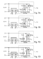
- FIGS. 7A through 7D illustrate an embodiment of anti-parallel active clamps for the power converter circuit.
- FIGS. 8A through 8D illustrate an embodiment of a primary side bidirectional freewheeling path for the power converter circuit.
- FIG. 9 illustrates various waveforms associated with the primary side bidirectional freewheeling path in FIGS. 8A through 8D .
- FIGS. 10A through 10D illustrate an embodiment of a secondary side bidirectional freewheeling path for the power converter circuit.
- FIG. 11 illustrates various waveforms associated with the secondary side bidirectional freewheeling path in FIGS. 10A through 10D .
- FIG. 12 illustrates a simplification of the secondary side bidirectional freewheeling path illustrated in FIGS. 10A through 100 .
- FIGS. 13A through 13C illustrate exemplary integration configurations for the bi-directional switch.
- FIG. 14 illustrates another embodiment of a power converter circuit devoid of a diode bridge rectifier on the primary (input) side, and which filters the AC mains frequency ripple of the AC input from the secondary side.
- FIG. 15 illustrates yet another embodiment of a power converter circuit devoid of a diode bridge rectifier on the primary (input) side, and which filters the AC mains frequency ripple of the AC input from the secondary side.
- FIGS. 16 and 17 illustrate embodiments of a clamping circuit for the bridgeless flyback converter.
- FIG. 18 illustrates different operating modes of the bridgeless flyback converter with the clamping circuit from FIGS. 16 and 17 .
- FIG. 19 illustrates various waveforms associated with the operation of bridgeless flyback converter in MODE 2.
- FIGS. 20, 21, 23, 24 and 26-27 illustrate the current flow paths in the power converter circuit during different conduction periods of MODE 2.
- FIG. 22 illustrates various waveforms associated with the operation of the bridgeless flyback converter in conduction period 2 of MODE 2.
- FIG. 25 illustrates various waveforms associated with the operation of the bridgeless flyback converter in conduction period 4 of MODE 2.
- FIGS. 28A through 28F illustrate the current flow paths in the power converter circuit during different conduction periods of MODE 5.
- FIG. 29 illustrates various waveforms associated with the operation of the bridgeless flyback converter in conduction period 6 of MODE 5.
- FIGS. 30 and 31 illustrates various waveforms associated with the operation of the bridgeless flyback converter in conduction period 2 of MODE 5.
- FIGS. 32A through 320 illustrate the current flow paths in the power converter circuit during different conduction periods of MODE 3.
- FIG. 33 illustrates various waveforms associated with the operation of the bridgeless flyback converter in MODE 3.
- FIGS. 34A through 34C illustrate the current flow paths in the power converter circuit during different conduction periods of MODE 6.
- FIG. 35 illustrates various waveforms associated with the operation of the bridgeless flyback converter in MODE 6.
- FIGS. 36A through 36C illustrate the current flow paths in the power converter circuit during different conduction periods of MODE 1.
- FIG. 37 illustrates various waveforms associated with the operation of the bridgeless flyback converter in MODE 1.
- FIGS. 38A through 380 illustrate the current flow paths in the power converter circuit during different conduction periods of MODE 4.
- FIG. 39 illustrates various waveforms associated with the operation of the bridgeless flyback converter in MODE 4.
- FIG. 40 illustrates a first embodiment of a start-up circuit on the secondary side of the bridgeless flyback converter.
- FIG. 41 illustrates a second embodiment of a start-up circuit on the secondary side of the bridgeless flyback converter.
- FIG. 42 illustrates a third embodiment of a start-up circuit on the secondary side of the bridgeless flyback converter.
- FIG. 43 illustrates various waveforms associated with the operation of the bridgeless flyback converter during a start-up phase.
- FIG. 44A illustrates various waveforms associated with the operation of the bridgeless flyback converter in conduction period A of the start-up phase.
- FIG. 44B illustrates various waveforms associated with the operation of the bridgeless flyback converter in conduction period B of the start-up phase.
- a power converter circuit has a bridgeless flyback converter with a primary (input) side electromagnetically coupled to a secondary (output) side by a transformer.
- the flyback converter is bridgeless in that the primary side is devoid of a diode bridge rectifier.
- An output capacitor is coupled to the secondary side of the bridgeless flyback converter, and a compensation stage is coupled in parallel with the output capacitor.
- the compensation stage is configured to store energy and regulate the voltage across the output capacitor.
- the input capacitor of the power converter on the primary side of the power converter has a capacitance such that the compensation stage filters the AC mains frequency ripple of the AC input from the secondary side.
- the input bulk capacitor size requirement can be reduced.
- the constraints that determine the physical size of the capacitor can be significantly mitigated and therefore the size minimized e.g. to the fundamental physical limit.
- the size of the bulk capacitor in a conventional arrangement when considering universal input voltage requirement, is determined by several constraints that must be met simultaneously. For example, a large capacitance value is needed to store sufficient energy when the AC input voltage is low such as low-line situation in the United States, which could be as low as 85 Vac.
- a second constraint is the voltage rating, meaning the dielectric must be able to withstand high-line conditions in Europe (264 Vac).
- the power converter circuit embodiments described herein also eliminate the rectifying diode bridge on the primary side. These embodiments, in concert with the secondary side AC line frequency filtering, address directly not only the physical size constraint by minimizing bulk capacitor size, but also the thermal constraint by eliminating the rectifying diode bridge and an arbitrarily large portion of the losses associated with it.
- the EMI filter is not directly addressed, nor the size or losses incurred by the EMI filter, however a reduction of both size and losses in the EMI filter can be realized through soft-switching properties of the converter circuits described herein as well as increased switching frequencies. By using soft-switching, an increase in switching frequency may be afforded, and through a combination of both soft-switching and increased switching frequency, the requirements to the EMI filter can be diminished.
- the range of frequencies the EMI filter must attenuate might be set on the lowest end by the fundamental of the switching frequency, which is intended to be increased, and on the highest end by the high order harmonic content of the voltages and currents inside, which are to a significant extent eliminated with soft-switching techniques.
- the losses associated with the EMI filter can be to some degree a function of peak-to-RMS current ratio, or at the very least the high-frequency content of the AC current at frequencies where the EMI filter inductor chokes are fundamentally and intentionally lossy.
- a bridgeless AC/DC adapter converter operating with almost purely low-frequency (e.g. 50-60 Hz) sinusoidal input current waveforms can ensure current flowing through the EMI chokes have near zero frequency content in the range, where these chokes are intentionally lossy. The losses associated with the EMI filter can thus be effectively minimized using the power converter circuit embodiments described herein.
- the power converter circuit embodiments described herein directly address the size associated with the bulk capacitor and losses associated with the diode bridge rectifier, both of which are fundamental limiters to power density in adapters, and both of which do not scale with switching frequency or by other traditional means.
- the EMI filter can scale by frequency, both in terms of physical size and losses.
- the power converter circuit embodiments described herein enable significantly high switching frequencies by offering soft-switching techniques (ZVS—zero voltage switching) and further benefits that can be derived by certain HEMT (high electron mobility transistor) device technology such as GaN devices with Bi-directional blocking capabilities and monolithic integration of several devices.
- FIG. 1 illustrates an embodiment of a power converter circuit 100 devoid of a diode bridge rectifier on the primary (input) side, and which filters the AC mains frequency ripple of the AC input from the secondary side.
- the power converter circuit 100 includes a bridgeless flyback converter 102 having a primary side electromagnetically coupled to a secondary side by a transformer 104 .
- the primary side is devoid of a diode bridge rectifier.
- the bridgeless flyback converter 102 is bidirectional in the sense that the bridgeless flyback converter operates from positive and negative input voltage (AC IN).
- the power converter circuit further includes an input capacitor Cin coupled to the primary side of the bridgeless flyback converter 102 , an output capacitor Cout coupled to the secondary side of the bridgeless flyback converter 102 , an EMI (electromagnetic interference) filter 106 coupled between the AC input and the input capacitor Cin, and a compensation stage 108 coupled in parallel with both the output capacitor Cout and the load 110 .
- the compensation stage includes a storage capacitor Cstore for storing energy, and regulates the voltage Vo across the output capacitor Cout.
- the input capacitor has a very small capacitance such that the compensation stage 108 filters the AC mains frequency ripple of the AC input from the secondary side.
- the bridgeless flyback converter 102 regulates the voltage across the storage capacitor Cstore of the compensation stage 108 .
- the compensation stage 108 can include a buck, boost or buck-boost converter coupled to the storage capacitor through an inductor.
- FIG. 2 illustrates an embodiment of the compensation stage 108 implemented as a buck converter.
- the buck converter includes a high-side switch device SP coupled between the voltage Vo across the output capacitor Cout and a common switch node SW, a low-side switch device SN coupled between the common switch node SW and a reference potential such as ground.
- the buck converter is coupled to the storage capacitor Cstore through an output inductor Lcom.
- the compensation stage of the power converter circuit 100 stores energy in the storage capacitor Cstore and regulates the voltage Vo across the output capacitor Cout as explained above, allowing for a reduction in the size of the input capacitor Cin.
- DCM discontinuous conduction mode
- CCM continuous conduction mode
- CRM critical conduction mode
- TOM triangular current mode
- the embodiments of the bridgeless flyback converter 102 shown in FIGS. 3A and 3B use high voltage (HV) back-to-back MOSFETs (metal-oxide-semiconductor field effect transistors) on the primary side and low voltage (LV) MOSFETs on the secondary side.
- HV high voltage
- LV low voltage
- the embodiment of the bridgeless flyback converter 102 shown in FIG. 3C uses HV GaN-based transistors having a bidirectional configuration on the primary side and LV GaN-based transistors having a bidirectional configuration on the secondary side. In each case, the bridgeless flyback converter 102 is bidirectional in that the converter 102 operates from positive and negative input voltage (AC IN).
- the transformer 104 used in topologies shown in FIGS.
- 3A through 3C has one primary side winding L 1 and two secondary side windings L 2 , L 3 .
- the secondary side windings L 2 , L 3 are in either a centre-tapped configuration as shown in FIGS. 3A through 3C , or a split-winding configuration separated by switches but operating fundamentally the same way.
- FIG. 3A illustrates an embodiment of the bridgeless flyback converter 102 in which a single bidirectional switch device on the primary side and formed by HV MOSFETs S 1 A and S 1 B in a source-to-source configuration, and a single secondary side switch SB plus a diode D 2 , D 3 for each secondary side winding L 2 , L 3 on the secondary side.
- All active switches S 1 A, S 1 B, SB operate in both AC input polarities, and therefore for the ideal case the polarity of the input voltage AC IN is not important for the control.
- diodes D 2 and D 3 have higher conduction losses compared to transistor devices.
- Diodes D 2 and D 3 and active switch SB can be repositioned in other configurations e.g. above the windings L 2 , L 3 or below.
- D 2 and D 3 can be replace with active MOSFETs as synchronous rectification switches to reduce conduction losses.
- FIG. 3B illustrates an embodiment of the bridgeless flyback converter 102 in which one bidirectional switch is connected in series with each winding L 1 , L 2 , L 3 of the transformer 104 .
- one bidirectional switch device is connected in series to the primary side winding L 1 of the transformer 104 .
- the primary side bidirectional switch device includes HV MOSFETs S 1 A and S 1 B shown in a source-to-source configuration.
- two bi-directional switch devices are shown each in a source-to-source configuration.
- the first bidirectional switch device on the secondary side includes LV MOSFETs S 2 A and S 2 B, and is connected in series to secondary side winding L 2 of the transformer 104 .
- the second bidirectional switch device on the secondary side includes LV MOSFETs S 3 A and S 3 B, and is connected in series to secondary side winding L 3 of the transformer 104 .
- Both secondary-side bidirectional switch devices can share the same source point (common source), and therefore can share the same isolated gate driver across all four transistors S 2 A, S 2 B, S 3 A, S 3 B.
- Conduction loss across the bidirectional switch devices on the secondary side should be lower compared to the dual diode plus MOSFET configuration shown in FIG. 3A .
- transistor S 2 A or S 3 A is not necessarily required.
- transistors S 2 A and S 3 A could operate in parallel to reduce on-state resistance R DSon .
- a drain-to-drain configuration is also possible as well as other separate configurations including two switches separated by the secondary side windings L 2 , L 3 .
- IGBTs insulated gate bipolar transistors
- other high voltage switches are also possible.
- FIG. 3C illustrates an embodiment of the bridgeless flyback converter 102 in which bidirectional GaN transistors are used to form the bidirectional switch devices on the primary and secondary sides of the converter 102 .
- Each bidirectional switch device S 1 , S 2 , S 3 includes two enhancement mode GaN HEMTs configured internally in a drain-to-drain manner. Due to the construction of GaN HEMTs, each pair of GaN HEMTs share the same drift region, lowering R DSon to almost the same value as a single transistor device. The result is a bidirectional blocking device with the conduction loss of a single device.
- FIG. 3C illustrates an embodiment of the bridgeless flyback converter 102 in which bidirectional GaN transistors are used to form the bidirectional switch devices on the primary and secondary sides of the converter 102 .
- Each bidirectional switch device S 1 , S 2 , S 3 includes two enhancement mode GaN HEMTs configured internally in a drain-to-drain manner. Due to the construction of GaN HEMTs, each
- the bidirectional switch device S 1 on the primary side is a high voltage GaN-based device and the bidirectional switch devices S 2 , S 3 on the secondary side are low voltage GaN-based devices. Because the GaN-based bidirectional switch devices S 1 , S 2 , S 3 each have effectively the same R DSon value as a single transistor, the conduction losses across the active devices are the same as a conventional flyback but eliminate the diode bridge losses.
- the bidirectional switch devices shown in FIGS. 3A through 3C allow the bridgeless flyback converter 102 to operate in a bidirectional manner in that current on the primary side can conduct in either direction as shown in FIGS. 4A through 4B and in FIGS. 5A through 5B .
- the current only conducts in one secondary side winding at any time. Operation during the positive AC input is illustrated in FIGS. 4A and 5A , and operation during the negative AC input is illustrated in FIGS. 4B and 5B .
- the curved line on the primary side shows the direction and conduction paths during the energizing state of the primary side winding L 1 .
- the curved lines on the secondary side show the direction and conduction paths during the de-energizing state of the secondary side windings L 2 , L 3 .
- FIG. 6 illustrates exemplary gate signals V G SXY&SXY for the primary and secondary side bidirectional switch devices and the current I LN through the corresponding transformer winding for the converter embodiment shown in FIG. 3B .
- the secondary side has bi-directional blocking and there is no natural body diode to allow transfer of energy to charge up the storage capacitor Cstore on the secondary side and wake up the secondary side control logic (not shown).
- a normally-on transistor device can be used for transistors SB, S 3 A or S 2 A. With a normally on device, a conduction path can occur during start-up.
- the circuit is still inherently safe since if transistor SB, S 3 A or S 2 A remains on in which the circuit can operate as a forward converter. Therefore, it is possible to operate the bridgeless flyback converter 102 in the same manner as a forward converter if required.
- the converter configurations shown in FIGS. 1 through 5B can be enhanced to improve performance and/or robustness.
- the converter 102 since the converter 102 is fundamentally a flyback, most soft switching concepts can be applied, including forced frequency ZVS (zero voltage switching) control, secondary side control with ZVS and other known soft switching control for flyback converters.
- ZVS zero voltage switching
- anti-parallel/bidirectional active clamps and bidirectional freewheeling techniques can also be utilized. Soft switching, anti-parallel/bidirectional active clamps and bidirectional freewheeling techniques and their application to the power converter circuit embodiments described above are described next in more detail.
- FIGS. 7A through 7D illustrate an embodiment of anti-parallel active clamps 112 incorporated into the power converter circuit 100 .
- the soft switching control must be aware in advance of the AC input polarity. This information is needed to turn on the correct switch and create the correct negative current signal for the right polarity.
- two active clamps 112 are coupled to the transformer primary side winding L 1 in parallel and in an inverted manner to recycle leakage energy of the transformer 104 in both directions.
- Each active clamp includes a clamp transistor SCA/SCB and a clamp capacitor C A /C B connected in series with the corresponding clamp transistor.
- FIGS. 7A and 7C show the conduction paths when the first active clamp is recycling energy from the leakage of the primary side winding L 1 and the bidirectional switch device formed by transistors S 1 A and S 1 B is blocking the AC input voltage plus the voltage generated from the primary side winding L 1 .
- the curved lines shown in FIGS. 7B and 7D show the ZVS currents from the clamp capacitors CA/CB driving the primary side winding L 1 in the reverse direction and driving the voltage of blocking transistors S 1 A and S 1 B towards zero when clamp transistors SCA and SCB are off.
- the storing of the leakage energy for the anti-parallel active clamps 112 is passive, and no control is required since the current simply conducts via the body diodes of clamp transistors SCA and SCB.
- the negative current to achieve ZVS on the primary side on any of the three windings L 1 , L 2 , L 3 will not only discharge the output capacitance of transistors S 1 A and S 1 B, it will also charge the output capacitance of one of the secondary side bi-directional switch devices, in this sense, the required negative current may be slightly higher than conventional control.
- FIGS. 8A through 8D illustrate an embodiment of a primary side bidirectional freewheeling path 114 incorporated into the power converter circuit 100 .
- the primary side bidirectional freewheeling path 114 includes a bi-directional switch device SC placed in parallel with the primary side winding L 1 of the transformer 104 .
- the bidirectional switch device SC can be any bidirectional switch device such as a bidirectional GaN or MOSFET switch device.
- FIG. 9 illustrates related waveforms associated with operation of the primary side bidirectional freewheeling path 114 illustrated in FIGS. 8A through 8D .
- V G SXY&SXY are the gate signals for the primary and secondary side bidirectional switch devices S 1 A/S 1 B, S 2 A/S 2 B, S 3 A/S 3 B and I LN represents the current through the respective transformer windings L 1 , L 2 , L 3 .
- secondary side switches S 3 A/S 3 B or S 2 A/S 2 B stay on for a short period to energize secondary side winding L 2 or L 3 in the reverse direction as shown by the curved lines in FIGS. 8A and 8C .
- secondary side switches S 3 A/S 3 B or S 2 A/S 2 B turn off and the bidirectional switch device SC turns on and the secondary side current is coupled to the primary side as a freewheeling current within the freewheeling path 114 , as shown by the curved lines in FIGS. 8B and 8D and by waveform IL 1 in FIG. 9 .
- the bidirectional switch device SC turns off, the freewheeling current drives the voltage of transistors S 1 A and S 1 B to zero.
- FIGS. 10A through 10D illustrate an embodiment of a secondary side bidirectional freewheeling path 116 incorporated into the power converter circuit 100 .
- the secondary side bidirectional freewheeling path 116 includes an additional switch SB on the secondary side to stop the output capacitor Cout from discharging through part of the secondary side freewheeling path 116 .
- the secondary side freewheeling path 116 is through transistors S 2 B and S 3 B on the secondary side via a common source connection, as well as going through both secondary windings L 2 , L 3 as indicated by the curved line in FIGS. 10B and 10D .
- FIG. 11 illustrates related waveforms associated with operation of the primary side bidirectional freewheeling path 114 illustrated in FIGS. 8A through 8D .
- FIG. 11 illustrates related waveforms associated with operation of the primary side bidirectional freewheeling path 114 illustrated in FIGS. 8A through 8D .
- V G SXY&SXY and V G SXY are the gate signals for the primary and secondary side bidirectional switch devices S 1 A/SIB, S 2 A/S 2 B, S 3 A/S 3 B and I LN represents the current through the respective transformer windings L 1 , L 2 . L 3 .
- transistors S 2 A and S 3 B turn off, freewheeling current again discharges the output capacitance of the primary side bidirectional switch device S 1 A/S 1 B. Higher conduction loss can occur on the secondary side due to the high number of switches in the conduction path.
- FIG. 12 illustrates a modification to the embodiment illustrated in FIGS. 10A through 10D .
- the modification reduces the number of switches by one, and simplifies the control and configuration on the secondary side where transistors S 2 A and S 2 B form a bidirectional switch device.
- Transistors S 3 A and S 3 B can also form a bidirectional switch device if their midpoints are accessible. If not, transistors S 3 A and S 3 B can be two synchronous rectification switches.
- a freewheeling path 116 is provided on the secondary side which conducts via only two transistors S 3 A and S 3 B without the need for the additional transistor SB shown in FIGS. 10A through 10D .
- the individual switches of the bridgeless flyback converter 102 can be monolithically integrated into a single die or co-packaged into a single package.
- the gate drivers can also be integrated, monolithically or co-packaged, into the package itself making the system small and potentially increasing the power density and efficiency for the converter circuit 100 .
- FIGS. 13A through 13C illustrate exemplary integration configurations.
- the devices included in each dashed box can be integrated into a single die or package.
- FIG. 13A illustrates different integration examples for the bridgeless flyback converter embodiment shown in FIG. 3A .
- FIG. 13B illustrates different integration examples for the bridgeless flyback converter embodiment shown in FIG. 3B .
- FIG. 13C illustrates different integration examples for the bridgeless flyback converter embodiment shown in FIG. 3C .
- FIG. 14 illustrates another embodiment of a power converter circuit 200 devoid of a diode bridge rectifier on the primary (input) side, and which filters the AC mains frequency ripple of the AC input from the secondary side.
- the embodiment shown in FIG. 14 is like the embodiment shown in FIG. 1 , with the bridgeless flyback converter 102 including the primary side bidirectional freewheeling path 114 shown in FIGS. 8A through 8D and minimised device count on the secondary side. If ZVS control is implemented, the requirement on the EMI filter 106 on the input can be reduced. This in turn can lead to higher power density and higher efficiency.
- the compensation stage 108 significantly reduces the size of the input capacitor Cin to a few ⁇ F, as previously described herein.
- the compensation stage 108 operates in both the forward and reverse direction.
- FIG. 15 illustrates yet another embodiment of a power converter circuit 300 devoid of a diode bridge rectifier on the primary (input) side, and which filters the AC mains frequency ripple of the AC input from the secondary side.
- the embodiment shown in FIG. 15 is like the embodiment shown in FIG. 14 , however the bidirectional freewheeling path 116 is implemented on the secondary side of the bridgeless flyback converter 102 as shown in FIGS. 10A through 10D .
- the power converter circuit 300 also has minimised device count on the secondary side as shown in FIG. 12 .
- ZVS zero voltage switching
- ZCS zero current switching
- Such switching control is achieved with a novel switching pattern and commutation path on the secondary side. Doing so significantly reduces the turn-on losses for all secondary side switches, and the switching loss of the bidirectional switch of the active clamp circuit is reduced, hence improving overall efficiency.
- FIG. 16 illustrates an embodiment of the bridgeless flyback converter 102 .
- the control strategy enables a snubbering function reducing energy dissipation, by adding an active clamp 400 to the bridgeless flyback converter topology.
- the snubbering function is realized by transferring energy stored into leakage inductance at the turn-off instant of primary side bidirectional switch device S 1 A/S 1 B into a clamping capacitor Cs, which is then discharged back into the AC source (AC IN) every half grid period (e.g. 100-120 Hz), thereby supplying energy back to the source or to the load 110 .
- AC IN AC source
- the active clamp 400 formed by capacitor Cs and bidirectional switch device SCA/SCB is essentially lossless in a bi-directional manner.
- part of the energy stored in the clamp capacitor is used to achieve ZVS for the primary side bidirectional switch device S 1 A/S 1 B.
- switch S 2 on the secondary side is blocking the path for current to charge the output capacitor Cout.
- This problem can solved by adding a normally on switch (S start ) in parallel to S 2 with relatively high R DSon on the secondary side.
- the equivalent circuit can be obtained by substituting the parallel connected switches S 2 and S start with the on resistance R DSon Start of normally-on switch S start as shown in FIG. 17 .
- the converter 102 is not controlled as a flyback as described in more detail later herein.
- the start-up phase lasts until the voltage Vo across the output capacitor Cout is high enough to adequately power gate drivers and control logic on the secondary side (not shown). Afterwards, normally-on switch S start is turned off and the converter 102 begins normal operation.
- the bridgeless flyback converter 102 operates in different modes depending on the phase of the input voltage Vin, as shown in FIG. 18 . Also plotted in FIG. 18 is the clamping voltage V Cclamp of capacitor Cs included in the active clamp 400 .
- the primary side of the bridgeless flyback converter 102 is operated as a buck-boost converter to pre-charge the clamping capacitor C s to a voltage equal to ⁇ V T .
- the secondary side of the bridgeless flyback converter 102 is disabled, so no energy is provided from the source to the load 110 and the load voltage is kept constant by the compensation stage 108 .
- the converter 102 operates as a flyback converter with a positive input voltage in this mode, and the secondary side is enabled and energy is provided from the source to the load 110 .
- the primary side of the bridgeless flyback converter 102 is operated as a buck-boost converter to discharge the clamping capacitor C s back to the AC source AC IN or discharge to the load. If discharge back to AC source, the secondary side is disabled, so no energy is provided from the source to the load 110 and the load voltage is kept constant by the compensation stage 108 .
- the primary side of the bridgeless flyback converter 102 is operated as a buck-boost converter to pre-charge the clamping capacitor C s to a voltage equal to V T .
- the secondary side is disabled, so no energy is provided from the source to the load 110 and the load voltage is kept constant by the compensation stage 108 .
- the converter 102 operates as a flyback converter with a negative input voltage during this mode, and the secondary side is enabled and energy is provided from the source AC IN to the load 110 .
- the primary side of the bridgeless flyback converter 102 is operated as a buck-boost converter to discharge the clamping capacitor C s back to the AC source AC IN or discharge to the load. If discharge back to AC source, the secondary side is disabled, so no energy is provided from the source to the load 110 and the load voltage is kept constant by the compensation stage 108 .
- the main operating modes of the bridgeless flyback converter 102 are MODE 2 and the MODE 5, wherein the topology is operated as a flyback converter with a positive and negative input voltage respectively and energy is transferred from the source AC IN to the load 110 .
- MODE 1 and MODE 4 are provided to pre-charge the clamping capacitor C s to a voltage equal to V T (with the correct polarity), to avoid discharging of the load 110 towards the clamping capacitor C s during the snubbering action of the active clamp 400 as will be explained later herein.
- MODE 3 and MODE 6 are provided to discharge the clamping capacitor C s and transfer energy stored in the clamping capacitor C s back to the source before the change of the grid polarity.
- the converter 102 can also transfer the stored energy to the load 110 instead of the source.
- PFC can be achieved during MODE 1, 2, 4 and 5.
- One method to achieve PFC is with constant on-time technique, which can be adjusted based on load conditions.
- MODE 2 and MODE 5 are the only modes where energy is supplied from the source AC IN to the load 110 . During these modes, the converter 102 operates as a flyback converter with positive and negative input voltage, respectively.
- the primary side bidirectional switch device of the converter 102 can be implemented as two unidirectional switches in drain-to-drain configuration with separate gate control. In another embodiment, the primary side bidirectional switch device can be implemented as two unidirectional switches in back-to-back configuration or as a monolithic bidirectional switch with two gates
- each switching cycle T sw is formed by seven conduction periods as shown in FIG. 19 .
- the switching cycles are described in more detail below in connection with FIG. 19 which illustrates waveforms of the current through the windings I L1 , I L2 , I L3 and of the output current I out in a switching period T sw for a positive input voltage.
- This conduction period is provided to charge the series of leakage and magnetizing inductance with a negative current I L1 to, in the next conduction period, discharge the output capacitance of the bidirectional switch S 1 and turn S 1 on under ZVS conditions.
- switch SCB is turned on as shown in FIG. 20 . Since the clamping capacitor C s is charged, negative current flows through the primary winding L 1 of the transformer 104 , thereby charging the magnetizing inductance of the transformer 104 . When this negative current has reached a threshold value, which allows to fully discharge the output capacitance of the bidirectional switch device S 1 A/S 1 B, this conduction period ends and the next conduction period begins.
- This conduction period is provided to discharge the output capacitance of the bidirectional switch device S 1 A/S 1 B and to turn S 1 A/S 1 B on under ZVS conditions in the next conduction period.
- switch S 1 A is turned on in ZVS and switch SOB is turned off as shown in FIGS. 21 and 22 .
- FIG. 22 illustrates waveforms of voltages and currents of the bidirectional switches S 1 A/S 1 B and SCA/SCB throughout a switching cycle Tsw for a positive input voltage. Since the leakage and magnetizing inductance drive a negative current I L1 , the output capacitance of switch SIB starts to get discharged by this current. When the discharge is completed, this conduction period ends and the next conduction period begins.
- Switches S 1 A and S 1 B which form the bidirectional switch S 1 A/S 1 B on the primary side of the bridgeless flyback converter 102 are both on while only switch SCA of the bidirectional switch SCA/SCB of the active clamp 400 is gated on.
- Current I L1 flows entirely through the primary winding L 1 , and increases linearly and charges the magnetizing inductance of the gapped transformer 104 .
- This current flows entirely through the bidirectional switch device S 1 A/SIB as shown in FIG. 22 . Since the current flows entirely through bidirectional switch device S 1 A/S 1 B, switch SCA is turned on at zero current (ZCS) and zero voltage switching (ZVS) and thus has zero turn-on loss.
- This conduction period is provided to discharge the output capacitance of the switch S 2 on the secondary side of the bridgeless flyback converter 102 to turn S 2 on under ZVS conditions in the next conduction period.
- switch S 3 A is briefly turned on as shown in FIG. 24 to allow a path on the secondary side for a negative current to discharge the output capacitance of switch S 2 and partially discharge the output capacitance the switch of S 3 B. This current tends to also discharge the output capacitor Cout, but since this conduction period lasts only for a very small fraction of the switching period, this discharge can be neglected.
- switch SCA Since this conduction period starts after the turn off-of bidirectional switch device S 1 A/S 1 B, switch SCA is kept on to provide a path on the primary side for the current to discharge the leakage inductance (snubbering function) and therefore prevent an overvoltage. This conduction period lasts until the output capacitance of switch S 2 is completely discharged as shown in FIG. 25 which illustrates zoomed waveforms of voltages and currents of switches S 2 , S 3 A, S 3 B around conduction MODES 2 and 3 for a positive input voltage.
- This conduction period is provided to discharge the output capacitance of switch S 3 B to turn S 3 B on under ZVS conditions in the next conduction period.
- the switch configuration and path of the current are shown in FIG. 26 .
- switch S 2 is turned on under ZVS conditions.
- the current charges the output capacitance of switch S 3 A and at the same time discharges the output capacitance of switch S 3 B.
- the output capacitance of switch S 3 B is completely discharged, the current flows entirely through switch S 2 and the body diode of switch S 3 B so this conduction period can end and switch S 3 B can be turned on under ZVS condition in the next conduction period.
- the magnetizing inductance of the transformer 104 is discharged to the load 110 .
- the converter switch configuration is shown in FIG. 27 and the corresponding waveforms of the current flowing through the secondary side windings L 2 , L 3 is shown in FIG. 19 .
- switch S 3 B is turned on under ZVS conditions to provide synchronous rectification while switch S 3 A is blocking. Under these switch conditions, the current flows only through the lower secondary winding L 3 of the transformer 104 and through switches S 3 B and S 2 to provide energy to the load 110 while no current flows through the upper secondary winding L 2 of the transformer 104 .
- This conduction period ends when the current flowing through winding L 3 becomes zero. At this point, switches S 2 and S 3 B are turned off under zero current switching (ZCS) conditions, essentially eliminating turn off losses.
- ZCS zero current switching
- the converter 102 is essentially idling and waiting for the end of the switching period since the converter 102 operates at a fixed frequency. As shown in FIG. 16 , all switches are off and no energy is provided to the load 100 and no energy is absorbed from the AC source AC IN during this conduction mode. A new switching cycle begins at the of this conduction period.
- each switching cycle T sw is formed by seven conduction modes as illustrated in FIG. 29 which shows waveforms of the current through the windings L 1 , L 2 , L 3 of the transformer 104 and of the output current Iout in a switching period Tsw for a negative input voltage.
- This conduction period is provided to charge the leakage and magnetizing inductance of the transformer 104 with a positive current I L1 to, in the next conduction period, discharge the output capacitance of bidirectional switch device S 1 A/S 1 B and to turn S 1 A/S 1 B on under ZVS conditions.
- switch SCA is turned on as shown in FIG. 28A . Since the clamping capacitor is charged as shown in FIG. 28A , positive current flows through the primary winding L 1 of the transformer 104 , charging the magnetizing inductance. When this positive current reaches a threshold value, which allows to fully discharge the output capacitance of bidirectional switch S 1 A/SIB, this conduction mode ends and the next conduction mode begins.
- This conduction period is provided to discharge the output capacitance of bidirectional switch S 1 A/S 1 B and to turn S 1 A/S 1 B on under ZVS conditions in the next conduction period.
- switch S 1 B is turned on in ZVS and switch SCA is turned off as shown in FIGS. 28B and 30 .
- FIG. 30 illustrates waveforms of voltages and currents of the bidirectional switches S 1 A/S 1 B and SCA/SCB throughout a switching cycle Tsw for a negative input voltage. Since the leakage and magnetizing inductance of the transformer 104 are driving a positive current I L1 , the output capacitance of switch S 1 A starts to get discharged by this current. When the discharge is completed, this conduction period ends and the next conduction period begins.
- Switches S 1 A and S 1 B which form the bidirectional switch S 1 A/S 1 B on the primary side of the converter 102 , are both on while only switch SCB of the bidirectional switch SCA/SCB is gated on.
- Current I L1 is negative and flows entirely through the primary winding L 1 of the transformer 104 , and decreases linearly to charge the magnetizing inductance of the gapped transformer 104 .
- This current flows entirely through bidirectional switch S 1 A/SIB as shown in FIG. 30 . Since the current flows entirely through bidirectional switch S 1 A/S 1 B switch SCB is turned on at zero current (ZCS) and zero voltage switching (ZVS), the turn-on loss of switch SCB is zero.
- This conduction period is provided to discharge the output capacitance of switch S 2 and to turn S 2 on under ZVS conditions in the next conduction period.
- switch S 3 B is briefly turned on as shown in FIG. 28D , to allow a path on the secondary side of the converter 102 for a negative current to discharge the output capacitance of switch S 2 and partially the discharge the output capacitance of switch S 3 A. This current tends to discharge the output capacitor Cout as well, but since this conduction period lasts only for a very small fraction of the switching period, this discharge can be neglected.
- switch SCB Since this conduction period starts after the turn off of bidirectional switch S 1 A/S 1 B, switch SCB is kept on to provide a path on the primary side of the converter 102 for the current to discharge the leakage inductance (snubbering function) of the transformer 104 and thereby prevent an overvoltage.
- This conduction period lasts until the output capacitance of switch S 2 is completely discharged as illustrated in FIG. 31 , which shows zoomed waveforms of voltages and currents of switches S 2 , S 3 A, S 3 B around conduction period 2 and 3 of MODE 5 for a negative input voltage.
- This conduction period is provided to discharge the output capacitance of switch S 3 A to turn S 3 A on under ZVS conditions in the next conduction period.
- the switch configuration and the current path are shown in FIG. 28E .
- switch S 2 is turned on under ZVS conditions.
- the current charges the output capacitance of switch S 3 B and at the same time discharges the output capacitance of switch S 3 A.
- the output capacitance of switch S 3 A is completely discharged, the current flows entirely through switch S 2 and the body diode of switch S 3 A so this conduction period can end and switch S 3 A can be turned on under ZVS condition in the next conduction period.
- the magnetizing inductance of the transformer 104 is discharged to the load 110 .
- the switch configuration of the converter 102 is shown in FIG. 28F and the waveform of the current flowing through the secondary side windings L 2 , L 3 of the transformer is shown in FIG. 29 .
- switch S 3 A is turned on under ZVS conditions to provide synchronous rectification while switch S 3 B is blocking.
- the current flows only through the lower secondary winding L 2 of the transformer 104 and through switches S 3 A and S 2 to provide energy to the load 110 while no current flows through the upper secondary winding L 3 of the transformer 104 .
- This conduction period ends when the current flowing through secondary winding L 2 becomes zero.
- switches S 2 and S 3 A are turned off under zero current switching (ZCS) conditions and their turn off losses are virtually eliminated.
- ZCS zero current switching
- the converter 102 is essentially idling and waiting for the end of the switching period since the converter 102 is operating at a fixed frequency. As shown in FIG. 16 , all switches are off and no energy is provided to the load 100 and no energy is absorbed from the AC source AC IN during this conduction period. A new switching cycle begins at the end of this conduction period.
- MODE 3 and MODE 6 are provided to discharge the clamping capacitor C s back to the source when the polarity of the input voltage Vin is positive and negative, respectively.
- the clamping capacitor C s is discharged back to the source so that the snubbing operation is performed properly.
- the clamping capacitor C s is charged positively (with the highest potential on the lower plate) when the input voltage polarity is positive and negatively (with the highest potential on the upper plate) when the input voltage polarity is negative.
- FIGS. 32A through 32C show the current path during conduction period A during MODE 3 and FIG. 32B shows the current path during conduction period B during MODE 3.
- switch S 1 A is gated on so bidirectional switch S 1 A/S 1 B on the primary side of the converter 102 effectively operates as a diode.
- switch SCA is kept on for the entire MODE 3 while switch SCB is switching. Accordingly, the bidirectional switch SCA/SCB is equivalent to a unidirectional switch.
- the equivalent circuit of the primary side of the converter 102 during MODE 3 is shown in FIG. 32C .
- the primary side can work in CCM, DCM or CRM. Next, only CRM is presented.
- the magnetizing inductance of the transformer 104 is charged with a linear negative current through the bidirectional switch SCA/SCB and the clamping capacitor C s is consequently discharging as desired.
- the magnetizing inductance of the transformer 104 is discharged with a linear negative current through the bidirectional switch S 1 A/S 1 B to the source AC IN. Since during this period the input current is negative while the input voltage is positive, power is provided back from the clamping capacitor C s to the source AC IN.
- FIG. 33 illustrates waveforms and gate signals over two switching periods for the primary winding L 1 of the transformer 104 , for the bidirectional switch S 1 A/S 1 B and for the bidirectional switch SCA/SCB during MODE 3.
- the clamping capacitor C s is charged negatively (the highest potential is on the upper plate) and the polarity of the input voltage Vin is negative.
- MODE 6 provides back to the source AC IN the energy stored into the clamping capacitor C s .
- the secondary side of the converter 102 is deactivated in MODE 6, and the primary side is controlled as a boost converter as shown in FIGS. 34A through 34C .
- FIG. 34A illustrates the current path during conduction period A of MODE 6 and FIG. 34B illustrates the current path during conduction period B of MODE 6.
- FIG. 35 illustrates waveforms and gate signals over two switching periods for the primary winding L 1 of the transformer 104 , for the bidirectional switch S 1 A/S 1 B and for the bidirectional switch SCA/SCB during MODE 6.
- switch S 1 B is gated on so bidirectional switch S 1 A/SIB effectively operates as a diode.
- switch SCB is kept on for all of MODE 6 while Switch SCA is switching.
- the bidirectional switch SCA/SCB is equivalent to a unidirectional switch.
- the equivalent circuit of the primary side of the converter 102 during this operation mode is shown in FIG. 34C .
- the diode and the unidirectional switch are simply flipped with respect to the ones in MODE 3.
- the primary side of the converter 102 can work in CCM, in DCM or CRM. Next, only CRM is presented.
- the magnetizing inductance of the transformer 104 is charged with a linear positive current through bidirectional switch SCA/SCB and the clamping capacitor C s is consequently discharging as desired.
- the magnetizing inductance of the transformer 104 is discharged with a linear positive decreasing current through bidirectional switch S 1 A/S 1 B to the source AC IN. Since during this phase the input current is positive while the input voltage Vin is negative, power is provided back from the clamping capacitor C s to the source AC IN.
- the clamping capacitor C s is pre-charged to a voltage value equal to VT every half switching period during MODE 1 and MODE 4.
- the diode on the primary side of the converter 102 will remain permanently forward biased so the current will flow from the output capacitor Cout, which will be discharged, to the clamping capacitor C s which will be charged.
- the converter 102 instead absorbs energy from the load (output capacitor) to charge the clamping capacitor C s . This is undesirable for two reasons. First, the output capacitor Cout is discharged when instead of being charged. Second, the negative current Iout which exits from Cout is only limited by the parasitic resistances of the components and therefore can be very high and potentially destructive.
- the clamping capacitor C s is pre-charged to a voltage at least equal to the one of the output capacitor Cout multiplied by the turn ratio n of the transformer 102 .
- the diode on the primary side of the converter 102 is reverse biased and no current flow throughs the diode, avoiding the discharging of the output capacitor Cout to the clamping capacitor C s .
- the input voltage V in is positive and the clamping capacitor C s starts initially discharged.
- the secondary side of the converter 102 is disabled and the primary side is operated as a buck-boost converter as shown in FIGS. 36A through 36C .
- FIG. 36A illustrates the current path during conduction period A of MODE 1.
- FIG. 36B illustrates the current path during conduction period B of MODE 1.
- FIG. 36C illustrates the equivalent circuit of the primary side during of the converter 102 during MODE 1.
- FIG. 37 illustrates waveforms and gate signals over two switching periods for bidirectional switch S 1 A/S 1 B and for bidirectional switch SCA/SCB on the primary side of the converter 102 .
- the magnetizing inductance of the transformer 104 is charged with a linear positive current through bidirectional switch S 1 A/S 1 B and the AC source AC IN whose polarity is positive.
- the magnetizing inductance of the transformer 104 is discharged with a linear positive decreasing current through bidirectional switch SCA/SCB to the clamping capacitor C s which is consequently charged positively.
- FIGS. 38A through 38C illustrate the input voltage V in and the clamping capacitor C s starts initially discharged.
- the secondary side of the converter 102 is disabled and the primary side is operated as a buck-boost converter as shown in FIGS. 38A through 38C .
- FIG. 38A illustrate the current path during conduction period A of MODE 4.
- FIG. 38B illustrates the current path during conduction period B of MODE 4.
- FIG. 38C illustrates the equivalent circuit of the primary side of the converter 102 during MODE 4.
- FIG. 39 illustrates waveforms and gate signals over two switching periods for bidirectional switch S 1 A/S 1 B and for bidirectional switch SCA/SCB on the primary side of the converter.
- the magnetizing inductance of the transformer 104 is charged with a linear negative current through bidirectional switch S 1 A/S 1 B and the AC source AC IN whose polarity is negative.
- the magnetizing inductance of the transformer 104 is discharged with a linear negative increasing current through bidirectional switch SCA/SCB to the clamping capacitor C s which is consequently charged negatively.
- the load 110 is disconnected from the converter 102 by a pass-transistor (not shown).
- a normally-on device is included on the secondary side of the converter 102 to provide a path for the current on the secondary side before the awakening the secondary side gate drivers and controller.
- FIG. 40 illustrates a first embodiment of a configuration that allows for the start-up of the converter 102 .
- switch device S 2 in FIGS. 16 and 17 is implemented as a normally-on device such as a normally-on GaN HEMT or a depletion mode MOSFET.
- FIG. 41 illustrates a second embodiment of a configuration that allows for the start-up of the converter 102 .
- switch device S 2 in FIGS. 16 and 17 is implemented as a normally-off device such as an enhancement mode MOSFET connected in parallel with a normally-on device S tart such as a GaN HEMT or a depletion mode MOSFET.
- FIG. 42 illustrates a third embodiment of a configuration that allows for the start-up of the converter 102 .
- switch device S 2 in FIGS. 16 and 17 is implemented as a normally-off device such as an enhancement mode MOSFET connected in parallel with a normally-on device S tart such as a GaN HEMT or a depletion mode MOSFET and a series-connected resistor R start .
- the normally-on switch S 2 is on so the converter 102 cannot be controlled as a flyback since it is not possible to block the current on the secondary side.
- the output capacitor C out is charged.
- the desired side effect of this pre-charging is a simultaneous charge of the clamping capacitor C s .
- FIG. 43 illustrates waveforms of the current IL 1 , IL 2 , IL 3 of the transformer windings L 1 , L 2 , L 3 and of the output current Iout during the start-up phase.
- FIG. 44A illustrates the current path during conduction period A of the start-up phase, in which bidirectional switch S 1 A/S 1 B and switch SCA on the primary side of the converter are turned on.
- the input current is positive and flows partly through the magnetizing inductance L, of the transformer 104 and partly through the upper secondary winding L 2 of the transformer 104 and charges the output capacitor C out .
- the current I Lm which flows through the magnetizing inductance of the transformer 104 is positive and linearly increasing as shown in FIG. 43 , while the current Iout flowing through the output capacitor Cout is constant and equal to:
- V in (t) and V out (t) are the values of the input voltage and of the output voltage, respectively, during the switching cycle under consideration.
- FIG. 44B illustrates the current path during conduction period B of the start-up phase, in which bidirectional switch S 1 A/S 1 B is turned off while switch SCA remains on.
- the magnetizing inductance of the transformer 104 is discharged with a linearly decreasing current. Part of this current flows through the clamping capacitor C s on the primary side of the converter 102 , and part of the current is transferred to the secondary side and charges the output capacitor Cout through the lower secondary winding L 3 of the transformer 104 , the body diode of switch S 3 B and normally-on device S 2 or S start .
- the output current during this phase is equal to:
- I out V Cclamp ⁇ ( t ) n - V out ⁇ ( t ) R start ( 2 )
- Equations (1) and (2) show that R start is the only limiting factor for the output current I out . For this reason, the on resistance R start of normally-on device S 2 or S start should be properly chosen to prevent the failure of the components of the converter 102 due to overcurrent.
- One embodiment to determine R start is to consider the worst case (maximum input voltage and output capacitor completely discharged) as follows:
Landscapes
- Engineering & Computer Science (AREA)
- Power Engineering (AREA)
- Physics & Mathematics (AREA)
- Electromagnetism (AREA)
- Dc-Dc Converters (AREA)
- Rectifiers (AREA)
Abstract
Description
where Vin(t) and Vout(t) are the values of the input voltage and of the output voltage, respectively, during the switching cycle under consideration.
Claims (19)
Priority Applications (2)
| Application Number | Priority Date | Filing Date | Title |
|---|---|---|---|
| US15/360,747 US10148169B2 (en) | 2016-11-23 | 2016-11-23 | Bridgeless flyback converter circuit and method of operating thereof |
| DE102017127729.3A DE102017127729A1 (en) | 2016-11-23 | 2017-11-23 | Bridgeless flyback circuit and method of operation thereof |
Applications Claiming Priority (1)
| Application Number | Priority Date | Filing Date | Title |
|---|---|---|---|
| US15/360,747 US10148169B2 (en) | 2016-11-23 | 2016-11-23 | Bridgeless flyback converter circuit and method of operating thereof |
Publications (2)
| Publication Number | Publication Date |
|---|---|
| US20180145595A1 US20180145595A1 (en) | 2018-05-24 |
| US10148169B2 true US10148169B2 (en) | 2018-12-04 |
Family
ID=62147943
Family Applications (1)
| Application Number | Title | Priority Date | Filing Date |
|---|---|---|---|
| US15/360,747 Active US10148169B2 (en) | 2016-11-23 | 2016-11-23 | Bridgeless flyback converter circuit and method of operating thereof |
Country Status (2)
| Country | Link |
|---|---|
| US (1) | US10148169B2 (en) |
| DE (1) | DE102017127729A1 (en) |
Families Citing this family (25)
| Publication number | Priority date | Publication date | Assignee | Title |
|---|---|---|---|---|
| US12144541B2 (en) | 2016-01-05 | 2024-11-19 | Boston Scientific Scimed, Inc. | Systems, apparatuses and methods for delivery of ablative energy to tissue |
| EP3749238B1 (en) | 2018-02-08 | 2023-08-16 | Farapulse, Inc. | Apparatus for controlled delivery of pulsed electric field ablative energy to tissue |
| EP3790483B1 (en) | 2018-05-07 | 2024-08-28 | Boston Scientific Scimed, Inc. | Systems for filtering high voltage noise induced by pulsed electric field ablation |
| CN115836908A (en) | 2018-05-07 | 2023-03-24 | 波士顿科学医学有限公司 | Systems, devices, and methods for delivering ablation energy to tissue |
| CN109256967B (en) * | 2018-10-26 | 2024-03-19 | 佛山市华全电气照明有限公司 | Constant voltage power supply circuit for stable power output during starting |
| CN109450241B (en) * | 2018-11-19 | 2019-11-29 | 阳光电源股份有限公司 | A kind of two-way DC/DC converter of two-stage type and its reverse starting control method |
| TWI696336B (en) * | 2019-04-12 | 2020-06-11 | 周重甫 | Flyback power switch architecture without bridge rectifier |
| US11424691B2 (en) * | 2019-07-03 | 2022-08-23 | Rohm Co., Ltd. | Switch driving device and switching power supply using the same |
| JP7386736B2 (en) * | 2019-07-03 | 2023-11-27 | ローム株式会社 | Switch drive device and switching power supply using the same |
| US10625080B1 (en) | 2019-09-17 | 2020-04-21 | Farapulse, Inc. | Systems, apparatuses, and methods for detecting ectopic electrocardiogram signals during pulsed electric field ablation |
| US11065047B2 (en) | 2019-11-20 | 2021-07-20 | Farapulse, Inc. | Systems, apparatuses, and methods for protecting electronic components from high power noise induced by high voltage pulses |
| US11497541B2 (en) | 2019-11-20 | 2022-11-15 | Boston Scientific Scimed, Inc. | Systems, apparatuses, and methods for protecting electronic components from high power noise induced by high voltage pulses |
| US10842572B1 (en) | 2019-11-25 | 2020-11-24 | Farapulse, Inc. | Methods, systems, and apparatuses for tracking ablation devices and generating lesion lines |
| CN111200307A (en) * | 2020-01-16 | 2020-05-26 | 珠海格力电器股份有限公司 | Energy balance control device, battery system and energy balance control method thereof |
| CN111509986A (en) * | 2020-05-19 | 2020-08-07 | 深圳英飞源技术有限公司 | Auxiliary slow start and discharge circuit of bidirectional phase-shifted full-bridge converter |
| KR102387123B1 (en) * | 2020-07-21 | 2022-04-15 | 한국항공우주연구원 | Ac-dc converter circuit system, and operating method of ac-dc converter circuit system |
| CN112003263A (en) * | 2020-09-16 | 2020-11-27 | 上海航天控制技术研究所 | Redundant secondary power supply circuit for combination of satellite-borne fiber-optic gyroscope |
| CN112636572B (en) * | 2020-12-04 | 2023-01-10 | 佛山市顺德区美的电子科技有限公司 | Air conditioner control method, device, equipment, air conditioner and medium |
| JP7633096B2 (en) * | 2021-06-09 | 2025-02-19 | ローム株式会社 | Switch driver and switching power supply using the same |
| US12237777B2 (en) * | 2021-06-15 | 2025-02-25 | Texas Instruments Incorporated | LLC converter and control |
| CN115706533A (en) * | 2021-08-17 | 2023-02-17 | 北京智芯微电子科技有限公司 | Control device for switching power supply and switching power supply |
| CN114629346B (en) * | 2022-04-28 | 2023-11-03 | 苏州浪潮智能科技有限公司 | Ethernet equipment, bidirectional converter and control method thereof |
| CN116208000B (en) * | 2023-05-04 | 2023-07-21 | 深圳市恒运昌真空技术有限公司 | A topology structure of a bidirectional isolation converter and the bidirectional isolation converter |
| CN117060748A (en) * | 2023-08-21 | 2023-11-14 | 哈尔滨工业大学 | Single-stage bridgeless isolated flyback rectifier based on dual-capacitor output structure |
| CN117060708B (en) * | 2023-08-21 | 2024-05-24 | 哈尔滨工业大学 | Single-stage bridgeless PFC converter and control method |
Citations (15)
| Publication number | Priority date | Publication date | Assignee | Title |
|---|---|---|---|---|
| US5218520A (en) * | 1991-11-27 | 1993-06-08 | Rozman Gregory I | Vscf system with reduced dc link ripple |
| US20080310201A1 (en) * | 2007-06-15 | 2008-12-18 | The Regents Of The University Of Colorado | Digital Power Factor Correction |
| US20100246215A1 (en) * | 2009-03-25 | 2010-09-30 | Kabushiki Kaisha Toyota Jidoshokki | Isolated dc-dc converter |
| US7903442B2 (en) * | 2006-11-30 | 2011-03-08 | Dell Products L.P. | Apparatus and methods for power conversion |
| US20120212986A1 (en) * | 2011-02-22 | 2012-08-23 | Minebea Co., Ltd. | Switching power supply apparatus |
| US8670250B2 (en) * | 2010-09-13 | 2014-03-11 | Futurewei Technologies, Inc. | Common mode noise reduction apparatus and method |
| US20140307484A1 (en) * | 2013-04-15 | 2014-10-16 | System General Corp. | Control circuit for active clamp flyback power converter with predicted timing control |
| US20140328097A1 (en) * | 2013-05-03 | 2014-11-06 | Traver Gumaer | Bridgeless boost power factor correction circuit for constant current input |
| US20150015071A1 (en) * | 2013-07-10 | 2015-01-15 | Infineon Technologies Austria Ag | Post-regulated flyback converter with variable output stage |
| US20150224885A1 (en) * | 2012-11-01 | 2015-08-13 | Myongji University Industry And Academia Cooperation Foundation | Device for compensating for ripples of output voltage of pfc converter and battery charging device for electric vehicle using same |
| US9318971B2 (en) | 2011-07-04 | 2016-04-19 | Panasonic Intellectual Property Management Co., Ltd. | Switching power supply apparatus |
| US20160276941A1 (en) * | 2015-03-19 | 2016-09-22 | Tdk Corporation | Series compensating electric power transmission system |
| US20160329814A1 (en) | 2015-05-07 | 2016-11-10 | Infineon Technologies Austria Ag | Voltage Conversion Method and Voltage Converter |
| US20170085183A1 (en) * | 2015-09-22 | 2017-03-23 | Infineon Technologies Austria Ag | System and Method for a Switched-Mode Power Supply Having a Transformer with a Plurality of Primary Windings |
| US20170271993A1 (en) * | 2016-03-19 | 2017-09-21 | Ionel Jitaru | Very High Efficiency One Stage Isolated Power Factor Correction Circuit |
-
2016
- 2016-11-23 US US15/360,747 patent/US10148169B2/en active Active
-
2017
- 2017-11-23 DE DE102017127729.3A patent/DE102017127729A1/en not_active Withdrawn
Patent Citations (15)
| Publication number | Priority date | Publication date | Assignee | Title |
|---|---|---|---|---|
| US5218520A (en) * | 1991-11-27 | 1993-06-08 | Rozman Gregory I | Vscf system with reduced dc link ripple |
| US7903442B2 (en) * | 2006-11-30 | 2011-03-08 | Dell Products L.P. | Apparatus and methods for power conversion |
| US20080310201A1 (en) * | 2007-06-15 | 2008-12-18 | The Regents Of The University Of Colorado | Digital Power Factor Correction |
| US20100246215A1 (en) * | 2009-03-25 | 2010-09-30 | Kabushiki Kaisha Toyota Jidoshokki | Isolated dc-dc converter |
| US8670250B2 (en) * | 2010-09-13 | 2014-03-11 | Futurewei Technologies, Inc. | Common mode noise reduction apparatus and method |
| US20120212986A1 (en) * | 2011-02-22 | 2012-08-23 | Minebea Co., Ltd. | Switching power supply apparatus |
| US9318971B2 (en) | 2011-07-04 | 2016-04-19 | Panasonic Intellectual Property Management Co., Ltd. | Switching power supply apparatus |
| US20150224885A1 (en) * | 2012-11-01 | 2015-08-13 | Myongji University Industry And Academia Cooperation Foundation | Device for compensating for ripples of output voltage of pfc converter and battery charging device for electric vehicle using same |
| US20140307484A1 (en) * | 2013-04-15 | 2014-10-16 | System General Corp. | Control circuit for active clamp flyback power converter with predicted timing control |
| US20140328097A1 (en) * | 2013-05-03 | 2014-11-06 | Traver Gumaer | Bridgeless boost power factor correction circuit for constant current input |
| US20150015071A1 (en) * | 2013-07-10 | 2015-01-15 | Infineon Technologies Austria Ag | Post-regulated flyback converter with variable output stage |
| US20160276941A1 (en) * | 2015-03-19 | 2016-09-22 | Tdk Corporation | Series compensating electric power transmission system |
| US20160329814A1 (en) | 2015-05-07 | 2016-11-10 | Infineon Technologies Austria Ag | Voltage Conversion Method and Voltage Converter |
| US20170085183A1 (en) * | 2015-09-22 | 2017-03-23 | Infineon Technologies Austria Ag | System and Method for a Switched-Mode Power Supply Having a Transformer with a Plurality of Primary Windings |
| US20170271993A1 (en) * | 2016-03-19 | 2017-09-21 | Ionel Jitaru | Very High Efficiency One Stage Isolated Power Factor Correction Circuit |
Non-Patent Citations (2)
| Title |
|---|
| Jong-Won Shin et al., High-Efficiency Bridgeless Flyback Rectifier With Bidirectional Switch and Dual Output Windings, IEEE Transactions on Power Electronics, vol. 29, No. 9, Sep. 2014. * |
| Shin, Jong-Won et al., "Bridgeless isolated PFC Rectifier Using Bidirectional Switch and Dual Output Windings", IEEE Energy Conversion Congress and Exposition (ECCE), Sep. 2011, pp. 2879-2884. |
Also Published As
| Publication number | Publication date |
|---|---|
| US20180145595A1 (en) | 2018-05-24 |
| DE102017127729A1 (en) | 2018-06-14 |
Similar Documents
| Publication | Publication Date | Title |
|---|---|---|
| US10148169B2 (en) | Bridgeless flyback converter circuit and method of operating thereof | |
| US7218081B2 (en) | Power system having multiple power converters with reduced switching loss | |
| US9705411B2 (en) | Soft-switched bidirectional buck-boost converters | |
| Panov et al. | Design and performance evaluation of low-voltage/high-current DC/DC on-board modules | |
| US8908401B2 (en) | Multiphase soft-switched DC-DC converter | |
| US5410467A (en) | Power converters with improved switching efficiency | |
| US5959438A (en) | Soft-switched boost converter with isolated active snubber | |
| US9812977B2 (en) | Resonant converters with an improved voltage regulation range | |
| US10637363B2 (en) | Converters with hold-up operation | |
| US6366474B1 (en) | Switching power supplies incorporating power factor correction and/or switching at resonant transition | |
| US10707767B2 (en) | Two-level switch driver for preventing avalanche breakdown for a synchronous rectification switch in a power converter operating in a low-power burst mode | |
| US9124190B2 (en) | Isolated switched mode power supply | |
| US9479048B2 (en) | Resonant isolated active power factor correction (PFC) rectifier | |
| US20150124487A1 (en) | Adjustable Resonant Apparatus for Power Converters | |
| US20120044722A1 (en) | Isolated switching converter | |
| US20080037293A1 (en) | Forward power converter controllers | |
| Das et al. | A novel load adaptive ZVS auxiliary circuit for PWM three-level DC–DC converters | |
| KR19980031946A (en) | Circuit for Zero-Voltage / Zero-Current Switching of Full-Bridge DC / DC Converters with Ripple Reduction of Output Current | |
| Yeh et al. | Light-load efficiency improvement for LLC converter with synchronous rectification in solid-state transformer application | |
| US20190052167A1 (en) | Method and Apparatus for Bidirectional Operation of Phase-Shift Full Bridge | |
| Mashhadi et al. | A dual-switch discontinuous current-source gate driver for a narrow on-time buck converter | |
| US7944188B1 (en) | Power converter circuits having bipolar outputs and bipolar inputs | |
| KR100572653B1 (en) | Current resonant switching power supply | |
| CN119096462A (en) | Improved Performance of Flyback Converters | |
| US6999325B2 (en) | Current/voltage converter arrangement |
Legal Events
| Date | Code | Title | Description |
|---|---|---|---|
| AS | Assignment |
Owner name: INFINEON TECHNOLOGIES AMERICAS CORP., CALIFORNIA Free format text: ASSIGNMENT OF ASSIGNORS INTEREST;ASSIGNORS:LIND, ANDERS SOREN;PERSSON, ERIC G.;SIGNING DATES FROM 20161129 TO 20170125;REEL/FRAME:041093/0731 Owner name: INFINEON TECHNOLOGIES AUSTRIA AG, AUSTRIA Free format text: ASSIGNMENT OF ASSIGNORS INTEREST;ASSIGNORS:FONTANA, NICO;LEONG, KENNITH KIN;REEL/FRAME:041093/0594 Effective date: 20161124 |
|
| AS | Assignment |
Owner name: INFINEON TECHNOLOGIES AUSTRIA AG, AUSTRIA Free format text: ASSIGNMENT OF ASSIGNORS INTEREST;ASSIGNOR:INFINEON TECHNOLOGIES AMERICAS CORP.;REEL/FRAME:043484/0308 Effective date: 20170822 |
|
| STCF | Information on status: patent grant |
Free format text: PATENTED CASE |
|
| CC | Certificate of correction | ||
| MAFP | Maintenance fee payment |
Free format text: PAYMENT OF MAINTENANCE FEE, 4TH YEAR, LARGE ENTITY (ORIGINAL EVENT CODE: M1551); ENTITY STATUS OF PATENT OWNER: LARGE ENTITY Year of fee payment: 4 |