US10120182B2 - Imaging systems with fluidic color filter elements - Google Patents
Imaging systems with fluidic color filter elements Download PDFInfo
- Publication number
- US10120182B2 US10120182B2 US15/283,707 US201615283707A US10120182B2 US 10120182 B2 US10120182 B2 US 10120182B2 US 201615283707 A US201615283707 A US 201615283707A US 10120182 B2 US10120182 B2 US 10120182B2
- Authority
- US
- United States
- Prior art keywords
- color filter
- fluid
- imaging sensor
- walls
- sensor defined
- Prior art date
- Legal status (The legal status is an assumption and is not a legal conclusion. Google has not performed a legal analysis and makes no representation as to the accuracy of the status listed.)
- Active, expires
Links
- 238000003384 imaging method Methods 0.000 title claims abstract description 54
- 239000012530 fluid Substances 0.000 claims abstract description 205
- 239000000758 substrate Substances 0.000 claims description 15
- 238000004140 cleaning Methods 0.000 claims description 13
- 239000011521 glass Substances 0.000 claims description 11
- VYPSYNLAJGMNEJ-UHFFFAOYSA-N Silicium dioxide Chemical compound O=[Si]=O VYPSYNLAJGMNEJ-UHFFFAOYSA-N 0.000 claims description 8
- 239000000110 cooling liquid Substances 0.000 claims description 7
- 235000012239 silicon dioxide Nutrition 0.000 claims description 4
- 239000000377 silicon dioxide Substances 0.000 claims description 4
- AMGQUBHHOARCQH-UHFFFAOYSA-N indium;oxotin Chemical compound [In].[Sn]=O AMGQUBHHOARCQH-UHFFFAOYSA-N 0.000 claims description 3
- 239000012780 transparent material Substances 0.000 claims description 3
- 239000012809 cooling fluid Substances 0.000 claims 1
- 239000010410 layer Substances 0.000 description 30
- 238000012545 processing Methods 0.000 description 13
- 238000001816 cooling Methods 0.000 description 7
- 239000000463 material Substances 0.000 description 7
- 239000007787 solid Substances 0.000 description 7
- 230000008901 benefit Effects 0.000 description 6
- 238000010586 diagram Methods 0.000 description 5
- 239000007788 liquid Substances 0.000 description 5
- 238000011109 contamination Methods 0.000 description 4
- 238000012864 cross contamination Methods 0.000 description 4
- LYCAIKOWRPUZTN-UHFFFAOYSA-N Ethylene glycol Chemical compound OCCO LYCAIKOWRPUZTN-UHFFFAOYSA-N 0.000 description 3
- KFZMGEQAYNKOFK-UHFFFAOYSA-N Isopropanol Chemical compound CC(C)O KFZMGEQAYNKOFK-UHFFFAOYSA-N 0.000 description 3
- DNIAPMSPPWPWGF-UHFFFAOYSA-N Propylene glycol Chemical compound CC(O)CO DNIAPMSPPWPWGF-UHFFFAOYSA-N 0.000 description 3
- 230000001413 cellular effect Effects 0.000 description 3
- 239000003086 colorant Substances 0.000 description 3
- 238000001914 filtration Methods 0.000 description 3
- 230000002209 hydrophobic effect Effects 0.000 description 3
- 238000009413 insulation Methods 0.000 description 3
- CSCPPACGZOOCGX-UHFFFAOYSA-N Acetone Chemical compound CC(C)=O CSCPPACGZOOCGX-UHFFFAOYSA-N 0.000 description 2
- XLOMVQKBTHCTTD-UHFFFAOYSA-N Zinc monoxide Chemical compound [Zn]=O XLOMVQKBTHCTTD-UHFFFAOYSA-N 0.000 description 2
- 238000006243 chemical reaction Methods 0.000 description 2
- 239000004020 conductor Substances 0.000 description 2
- 238000000034 method Methods 0.000 description 2
- 230000005855 radiation Effects 0.000 description 2
- XLYOFNOQVPJJNP-UHFFFAOYSA-N water Substances O XLYOFNOQVPJJNP-UHFFFAOYSA-N 0.000 description 2
- YCKRFDGAMUMZLT-UHFFFAOYSA-N Fluorine atom Chemical compound [F] YCKRFDGAMUMZLT-UHFFFAOYSA-N 0.000 description 1
- 229910052581 Si3N4 Inorganic materials 0.000 description 1
- ATJFFYVFTNAWJD-UHFFFAOYSA-N Tin Chemical compound [Sn] ATJFFYVFTNAWJD-UHFFFAOYSA-N 0.000 description 1
- 229910052782 aluminium Inorganic materials 0.000 description 1
- XAGFODPZIPBFFR-UHFFFAOYSA-N aluminium Chemical compound [Al] XAGFODPZIPBFFR-UHFFFAOYSA-N 0.000 description 1
- 238000003491 array Methods 0.000 description 1
- 230000005540 biological transmission Effects 0.000 description 1
- 230000009977 dual effect Effects 0.000 description 1
- 239000000975 dye Substances 0.000 description 1
- 230000005684 electric field Effects 0.000 description 1
- 229910052731 fluorine Inorganic materials 0.000 description 1
- 239000011737 fluorine Substances 0.000 description 1
- 229910003437 indium oxide Inorganic materials 0.000 description 1
- PJXISJQVUVHSOJ-UHFFFAOYSA-N indium(iii) oxide Chemical compound [O-2].[O-2].[O-2].[In+3].[In+3] PJXISJQVUVHSOJ-UHFFFAOYSA-N 0.000 description 1
- 239000000203 mixture Substances 0.000 description 1
- 238000012986 modification Methods 0.000 description 1
- 230000004048 modification Effects 0.000 description 1
- 230000003287 optical effect Effects 0.000 description 1
- 150000002894 organic compounds Chemical class 0.000 description 1
- 239000000049 pigment Substances 0.000 description 1
- 230000010287 polarization Effects 0.000 description 1
- 230000004044 response Effects 0.000 description 1
- 238000005070 sampling Methods 0.000 description 1
- HQVNEWCFYHHQES-UHFFFAOYSA-N silicon nitride Chemical compound N12[Si]34N5[Si]62N3[Si]51N64 HQVNEWCFYHHQES-UHFFFAOYSA-N 0.000 description 1
- 239000002356 single layer Substances 0.000 description 1
- 238000010897 surface acoustic wave method Methods 0.000 description 1
- XOLBLPGZBRYERU-UHFFFAOYSA-N tin dioxide Chemical compound O=[Sn]=O XOLBLPGZBRYERU-UHFFFAOYSA-N 0.000 description 1
- 229910001887 tin oxide Inorganic materials 0.000 description 1
- 238000012546 transfer Methods 0.000 description 1
- 238000009736 wetting Methods 0.000 description 1
- 239000011787 zinc oxide Substances 0.000 description 1
Images


Classifications
-
- G—PHYSICS
- G02—OPTICS
- G02B—OPTICAL ELEMENTS, SYSTEMS OR APPARATUS
- G02B26/00—Optical devices or arrangements for the control of light using movable or deformable optical elements
- G02B26/004—Optical devices or arrangements for the control of light using movable or deformable optical elements based on a displacement or a deformation of a fluid
-
- G—PHYSICS
- G02—OPTICS
- G02B—OPTICAL ELEMENTS, SYSTEMS OR APPARATUS
- G02B26/00—Optical devices or arrangements for the control of light using movable or deformable optical elements
- G02B26/007—Optical devices or arrangements for the control of light using movable or deformable optical elements the movable or deformable optical element controlling the colour, i.e. a spectral characteristic, of the light
-
- G—PHYSICS
- G02—OPTICS
- G02B—OPTICAL ELEMENTS, SYSTEMS OR APPARATUS
- G02B5/00—Optical elements other than lenses
- G02B5/20—Filters
- G02B5/201—Filters in the form of arrays
-
- H—ELECTRICITY
- H01—ELECTRIC ELEMENTS
- H01L—SEMICONDUCTOR DEVICES NOT COVERED BY CLASS H10
- H01L27/00—Devices consisting of a plurality of semiconductor or other solid-state components formed in or on a common substrate
- H01L27/14—Devices consisting of a plurality of semiconductor or other solid-state components formed in or on a common substrate including semiconductor components sensitive to infrared radiation, light, electromagnetic radiation of shorter wavelength or corpuscular radiation and specially adapted either for the conversion of the energy of such radiation into electrical energy or for the control of electrical energy by such radiation
- H01L27/144—Devices controlled by radiation
- H01L27/146—Imager structures
- H01L27/14601—Structural or functional details thereof
- H01L27/1462—Coatings
- H01L27/14621—Colour filter arrangements
-
- H—ELECTRICITY
- H01—ELECTRIC ELEMENTS
- H01L—SEMICONDUCTOR DEVICES NOT COVERED BY CLASS H10
- H01L27/00—Devices consisting of a plurality of semiconductor or other solid-state components formed in or on a common substrate
- H01L27/14—Devices consisting of a plurality of semiconductor or other solid-state components formed in or on a common substrate including semiconductor components sensitive to infrared radiation, light, electromagnetic radiation of shorter wavelength or corpuscular radiation and specially adapted either for the conversion of the energy of such radiation into electrical energy or for the control of electrical energy by such radiation
- H01L27/144—Devices controlled by radiation
- H01L27/146—Imager structures
- H01L27/14643—Photodiode arrays; MOS imagers
- H01L27/14645—Colour imagers
-
- H—ELECTRICITY
- H04—ELECTRIC COMMUNICATION TECHNIQUE
- H04N—PICTORIAL COMMUNICATION, e.g. TELEVISION
- H04N23/00—Cameras or camera modules comprising electronic image sensors; Control thereof
- H04N23/20—Cameras or camera modules comprising electronic image sensors; Control thereof for generating image signals from infrared radiation only
-
- H—ELECTRICITY
- H04—ELECTRIC COMMUNICATION TECHNIQUE
- H04N—PICTORIAL COMMUNICATION, e.g. TELEVISION
- H04N25/00—Circuitry of solid-state image sensors [SSIS]; Control thereof
- H04N25/10—Circuitry of solid-state image sensors [SSIS]; Control thereof for transforming different wavelengths into image signals
- H04N25/11—Arrangement of colour filter arrays [CFA]; Filter mosaics
- H04N25/13—Arrangement of colour filter arrays [CFA]; Filter mosaics characterised by the spectral characteristics of the filter elements
- H04N25/131—Arrangement of colour filter arrays [CFA]; Filter mosaics characterised by the spectral characteristics of the filter elements including elements passing infrared wavelengths
-
- H—ELECTRICITY
- H04—ELECTRIC COMMUNICATION TECHNIQUE
- H04N—PICTORIAL COMMUNICATION, e.g. TELEVISION
- H04N5/00—Details of television systems
- H04N5/30—Transforming light or analogous information into electric information
- H04N5/33—Transforming infrared radiation
-
- H04N9/045—
Definitions
- This relates generally to imaging devices, and more particularly, to imaging devices having color filter elements.
- Image sensors are commonly used in electronic devices such as cellular telephones, cameras, and computers to capture images.
- an image sensor includes an array of image pixels arranged in pixel rows and pixel columns. Circuitry may be coupled to each pixel column for reading out image signals from the image pixels.
- the color filter elements filter incident light to allow only light of a desired wavelength to reach the underlying pixel.
- the solid color filter elements of conventional imaging pixels are inflexible. After the sensor is made, the solid color filter elements cannot be easily modified to enable different desired color filter element characteristics.
- FIG. 1 is a diagram of an illustrative electronic device having an image sensor and processing circuitry for capturing images using an array of image pixels in accordance with an embodiment.
- FIG. 2 is a diagram of an illustrative pixel array and associated readout circuitry for reading out image signals from the pixel array in accordance with an embodiment.
- FIG. 3 is a schematic diagram of an illustrative fluidic color filter system for an electronic device in accordance with an embodiment.
- FIG. 4 is a cross-sectional side view of illustrative fluidic color filter elements of an image sensor in accordance with an embodiment.
- FIG. 5 is a top view of illustrative color filter chambers filled with color filter fluids in accordance with an embodiment.
- FIGS. 6 and 7 are top views of illustrative color filter chambers that include color filter elements arranged in groups in accordance with an embodiment.
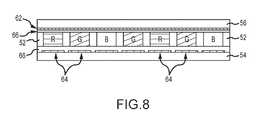
- FIG. 8 is a cross-sectional side view of illustrative fluidic color filter elements that are controlled using electrowetting in accordance with an embodiment.
- Electronic devices such as digital cameras, computers, cellular telephones, and other electronic devices may include image sensors that gather incoming light to capture an image.
- the image sensors may include arrays of image pixels.
- the pixels in the image sensors may include photosensitive elements such as photodiodes that convert the incoming light into image signals.
- Image sensors may have any number of pixels (e.g., hundreds or thousands or more).
- a typical image sensor may, for example, have hundreds of thousands or millions of pixels (e.g., megapixels).
- Image sensors may include control circuitry such as circuitry for operating the image pixels and readout circuitry for reading out image signals corresponding to the electric charge generated by the photosensitive elements.
- FIG. 1 is a diagram of an illustrative imaging system such as an electronic device that uses an image sensor to capture images.
- Electronic device 10 of FIG. 1 may be a portable electronic device such as a camera, a cellular telephone, a tablet computer, a webcam, a video camera, a video surveillance system, an automotive imaging system, a video gaming system with imaging capabilities, or any other desired imaging system or device that captures digital image data.
- Camera module 12 may be used to convert incoming light into digital image data.
- Camera module 12 may include one or more lenses 14 and one or more corresponding image sensors 16 .
- Lenses 14 may include fixed and/or adjustable lenses and may include microlenses formed on an imaging surface of image sensor 16 .
- Image sensor 16 may include circuitry for converting analog pixel data into corresponding digital image data to be provided to storage and processing circuitry 18 .
- camera module 12 may be provided with an array of lenses 14 and an array of corresponding image sensors 16 .
- Storage and processing circuitry 18 may include one or more integrated circuits (e.g., image processing circuits, microprocessors, storage devices such as random-access memory and non-volatile memory, etc.) and may be implemented using components that are separate from camera module 12 and/or that form part of camera module 12 (e.g., circuits that form part of an integrated circuit that includes image sensors 16 or an integrated circuit within module 12 that is associated with image sensors 16 ).
- Image data that has been captured by camera module 12 may be processed and stored using processing circuitry 18 (e.g., using an image processing engine on processing circuitry 18 , using an imaging mode selection engine on processing circuitry 18 , etc.).
- Processed image data may, if desired, be provided to external equipment (e.g., a computer, external display, or other device) using wired and/or wireless communications paths coupled to processing circuitry 18 .
- Image sensor 16 and processing circuitry 18 may be implemented using a stacked-chip arrangement if desired.
- image sensor 16 may include a pixel array 20 containing image sensor pixels 22 arranged in rows and columns (sometimes referred to herein as image pixels or pixels) and control and processing circuitry 24 .
- Array 20 may contain, for example, hundreds or thousands of rows and columns of image sensor pixels 22 .
- Control circuitry 24 may be coupled to row control circuitry 26 and image readout circuitry 28 (sometimes referred to as column control circuitry, readout circuitry, processing circuitry, or column decoder circuitry).
- Row control circuitry 26 may receive row addresses from control circuitry 24 and supply corresponding row control signals such as reset, row-select, charge transfer, dual conversion gain, and readout control signals to pixels 22 over row control paths 30 .
- One or more conductive lines such as column lines 32 may be coupled to each column of pixels 22 in array 20 .
- Column lines 32 may be used for reading out image signals from pixels 22 and for supplying bias signals (e.g., bias currents or bias voltages) to pixels 22 .
- bias signals e.g., bias currents or bias voltages
- a pixel row in array 20 may be selected using row control circuitry 26 and image signals generated by image pixels 22 in that pixel row can be read out along column lines 32 .
- Image readout circuitry 28 may receive image signals (e.g., analog pixel values generated by pixels 22 ) over column lines 32 .
- Image readout circuitry 28 may include sample-and-hold circuitry for sampling and temporarily storing image signals read out from array 20 , amplifier circuitry, analog-to-digital conversion (ADC) circuitry, bias circuitry, column memory, latch circuitry for selectively enabling or disabling the column circuitry, or other circuitry that is coupled to one or more columns of pixels in array 20 for operating pixels 22 and for reading out image signals from pixels 22 .
- ADC circuitry in readout circuitry 28 may convert analog pixel values received from array 20 into corresponding digital pixel values (sometimes referred to as digital image data or digital pixel data).
- Image readout circuitry 28 may supply digital pixel data to control and processing circuitry 24 and/or processor 18 ( FIG. 1 ) over path 25 for pixels in one or more pixel columns.
- image pixels 22 may include one or more photosensitive regions for generating charge in response to image light. Photosensitive regions within image pixels 22 may be arranged in rows and columns on array 20 .
- Pixel array 20 may be provided with a color filter array having multiple color filter elements which allows a single image sensor to sample light of different colors.
- image sensor pixels such as the image pixels in array 20 may be provided with a color filter array which allows a single image sensor to sample red, green, and blue (RGB) light using corresponding red, green, and blue image sensor pixels arranged in a Bayer mosaic pattern.
- RGB red, green, and blue
- the Bayer mosaic pattern consists of a repeating unit cell of two-by-two image pixels, with two green image pixels diagonally opposite one another and adjacent to a red image pixel diagonally opposite to a blue image pixel.
- the green pixels in a Bayer pattern are replaced by broadband image pixels having broadband color filter elements (e.g., clear color filter elements, yellow color filter elements, etc.).
- broadband color filter elements e.g., clear color filter elements, yellow color filter elements, etc.
- the color filter elements used to cover pixels 22 may be formed from fluids.
- the fluidic color filter elements may be controllable such that fluids of different colors can be used to cover each pixel. For example, a pixel may be covered by a red color filter fluid in a first operating mode and may be covered by a blue color filter fluid in a second operating mode.
- FIG. 3 A schematic diagram of an imaging system with fluidic color filter elements is shown in FIG. 3 .
- the imaging system may include one or more fluid reservoirs 42 .
- FIG. 3 provides a number of examples of fluids that may be included in imaging system 10 .
- red color filter fluid reservoir 42 - 1 green color filter fluid reservoir 42 - 2 , blue color filter fluid reservoir 42 - 3 , infrared color filter fluid reservoir 42 - 4 , ultraviolet color filter fluid reservoir 42 - 5 , cleaning solution reservoir 42 - 6 , and cooling liquid reservoir 42 - 7 may be included in fluid reservoirs 42 .
- These examples of fluid reservoirs are merely illustrative, and any desired fluid reservoirs may be included.
- the fluid reservoirs may be coupled to inlets/outlets 44 .
- the inlets/outlets may couple fluid from the fluid reservoirs to color filter chambers 46 .
- the color filter chambers may be chambers above the pixels.
- the color filter chambers may be formed above photodiodes of pixels 22 .
- the color filter chambers may be interposed between photodiodes and microlenses for the pixels. Each color filter chamber may cover any desired subset of pixels in the image sensor.
- one color filter chamber may cover only one pixel in the sensor, may cover all of the pixels in the sensor, may cover 25% of the pixels in the sensor, may cover 50% of the pixels in the sensor, may cover 33% of the pixels in the sensor, may cover 10%-50% of the pixels in the sensor, may cover 10%-30% of the pixels in the sensor, may cover less than 15% of the pixels in the sensor, may cover greater than 10% of the pixels in the sensor, may cover 40%-60% of the pixels in the sensor, or may cover some other desired subset of the pixels in the sensor.
- each color filter chamber may cover only one pixel, more than one pixel, more than ten pixels, more than one hundred pixels, more than one thousand pixels, less than one thousand pixels, less than one hundred pixels, or any other desired number of pixels.
- One color filter arrangement that may be used in the imaging system is a Bayer color filter pattern of red, green, and blue pixels.
- One color filter chamber may be associated with the red pixels in the Bayer color filter pattern, one color filter chamber may be associated with the green pixels in the Bayer color filter pattern, and one color filter chamber may be associated with the blue pixels in the Bayer color filter pattern.
- the chamber associated with the green pixels may be emptied of color filter fluid, and the chamber may be filled with broadband color filter fluid.
- Each chamber may be coupled to a respective inlet/outlet.
- the inlet/outlet may allow color filter fluid to enter and exit the chamber and may sometimes be referred to as simply an inlet.
- Each inlet may be capable of receiving fluid from any reservoir in fluid reservoirs 42 .
- control circuitry 48 may be able to direct fluid from a specific fluid reservoir to a particular inlet.
- a color filter chamber may cover approximately 25% of the pixels in the image sensor.
- the color filter chamber may be coupled to an inlet.
- the control circuitry may direct red color filter fluid from red color filter fluid reservoir 42 - 1 to the inlet to fill the color filter chamber.
- the sensor may later change to an infrared image sensing mode.
- the red color filter fluid may be drained from the color filter chamber and returned to red color filter reservoir 42 - 1 .
- infrared color filter fluid from infrared color filter fluid reservoir 42 - 4 may be sent to the color filter chamber through the inlet.
- the sensor may later change to a monochrome imaging mode.
- the infrared color filter fluid may be replaced with monochrome color filter fluid used to obtain black and white images.
- the sensor may adapt to low light conditions by switching to a clear filter to absorb as much light as possible.
- Any desired equipment may be included in the imaging system to move color filter fluid amongst the system in a controlled way.
- one or more pumps may be included in the system.
- the control circuitry may couple a desired reservoir to a desired color filter chamber using one of the inlets.
- the control circuitry may then direct a pump in the reservoir to pump the color filter liquid into the color filter chamber.
- Electrowetting, optoelectrowetting, and surface acoustic waves may all be used to control the fluid flow. If desired, different color filter fluids may be deliberately mixed to form an additional color filter fluid.
- the imaging system may include fluid of any desired type to fill color filter chambers.
- the fluid may be formed from any desired materials (i.e., organic compounds, dyes, pigments, etc.).
- Each reservoir may have a fluid with desired color filter properties.
- a color filter fluid in a reservoir may be configured to filter light of a particular visible wavelength (i.e., red color filter fluid reservoir 42 - 1 , green color filter fluid reservoir 42 - 2 , blue color filter fluid reservoir 42 - 3 , etc.).
- the color filter fluid may act as a broadband color filter (i.e., passing yellow or white light).
- the color filter fluids are not limited to only filtering visible light.
- an infrared color filter fluid i.e., infrared color filter fluid reservoir 42 - 4
- the infrared color filter fluid may be used in an infrared mode.
- the infrared color filter fluid may be used to cover all of the pixels in the sensor.
- the infrared color filter fluid may be used to cover some of the pixels in the sensor, and visible light filter fluids may be used to cover other pixels in the sensor.
- fluid reservoirs 42 may include more than one type of infrared color filter fluid.
- a first color filter fluid may be configured to pass near-infrared light while a second color filter fluid may be configured to pass long-wavelength infrared light.
- a first color filter fluid may be configured to pass near-infrared light of a first wavelength (i.e., 940 nm) while a second color filter fluid may be configured to pass near-infrared light of a second wavelength (i.e., 1085 nm).
- the color filter fluid may filter ultraviolet light (e.g., ultraviolet color filter fluid 42 - 5 ) or other types of light.
- ultraviolet light e.g., ultraviolet color filter fluid 42 - 5
- any number of fluid reservoirs may be included to pass any desired type of light.
- Each color filter fluid may pass light of any desired wavelength.
- the color filter fluids may be used in any combination.
- the refractive index of the color filter fluids may be used for additional functionality. For example, a particular fluid's refractive index could be used to switch a pixel on or off based on changing between transmission and total internal reflection. Similarly, the color filter fluid may alter the polarization of incoming light.
- the color filter fluid may offer cooling benefits.
- Recirculation of the color filter fluids may offer cooling benefits for the imaging system. These benefits may sometimes be obtained passively. For example, if the color filter liquid is changed from a first liquid to a second liquid, there will likely be some cooling benefits (even if the change was made for other reasons).
- the system may actively take advantage of the cooling properties of the fluidic color filter system. For example, even if the optical properties of the color filters do not need to change, the color filter fluid may be recirculated to help cool the sensor.
- the color filter fluids may be returned from the color filter chambers to their respective fluid reservoirs then sent back to the color filter chambers to help cool the imaging sensor.
- a fluid may be included specifically for its cooling properties (i.e., cooling liquid 42 - 7 ). If cooling the system is desired, the chambers may be evacuated of color filter fluid and filled with the cooling liquid. When the cooling is complete, the cooling liquid may be returned to its reservoir and the color filter chambers may be refilled with color filter fluid.
- the cooling liquid may be formed from any desired materials (i.e., water, ethylene glycol, propylene glycol, etc.).
- One possible obstacle to the performance of the fluidic color filter system is the cross-contamination of the color filter fluids. For example, take a scenario where a color filter chamber is filled with red color filter fluid. It is then desired to switch the red color filter fluid to green color filter fluid. Accordingly, the red color filter fluid is removed from the chamber. Ideally, all of the red color filter fluid would be evacuated from the chamber when desired. However, it is possible that some red color filter fluid residue will remain in the chamber after evacuation. If this occurs, the green color filter fluid will fill the chamber and mix with the red color filter fluid residue. Depending on the amount of residue, the performance of the green color filter fluid may be degraded. In one switch of the color filter fluids, the contamination may be negligible to performance of the color filter fluids. However, the color filter fluids may be switched regularly, causing the contamination to increase steadily over time. Clearly, it is desirable to eliminate any contamination between color filter fluids if possible.
- a dedicated cleaning solution may be included in a fluid reservoir.
- cleaning solution reservoir 42 - 6 may be included in fluid reservoirs 42 .
- the cleaning solution may be used to flush the color filter chambers when a switch in color filter fluids occurs.
- a red color filter fluid may be changed to a green color fluid. After the red color filter fluid is removed from the color filter chamber, cleaning solution 42 - 6 may temporary fill the chamber and then return to its reservoir. After the cleaning solution has flushed the color filter chamber, the green color filter fluid may fill the color filter chamber.
- the cleaning solution may therefore help reduce any contamination between the red and green color filter fluids (because any red color filter fluid residue would be mixed with cleaning solution 42 - 6 instead of green color filter fluid 42 - 2 ).
- Cleaning solution 42 - 6 may be used to fill any desired color filter chamber at any desired time.
- Cleaning solution 42 - 6 may include any desired material (e.g., acetone, isopropyl alcohol).
- fluid reservoirs 42 may be replaceable. Each fluid reservoir may be individually replaceable or the entire bank of fluid reservoirs may be replaceable.
- the imaging system may present an indication to the user that one or more color filter fluids need to be replaced, and the user may replace the color filter fluid reservoirs accordingly.
- FIG. 4 is a cross-sectional side view of an illustrative imaging sensor with a fluidic color filter system.
- fluidic color filter elements 58 may be included between layers 54 and 56 .
- Blue color filter elements are labelled with a “B”
- red color filter elements are labelled with an “R”
- green color filter elements are labeled with a “G.”
- Layer 54 (sometimes referred to as substrate 54 ) may include one or more photodiodes per fluidic color filter element. In some cases, there may be one color filter element per each photodiode in substrate 54 .
- each color filter element may cover more than one photodiode in substrate 54 (i.e., two photodiodes, three photodiodes, four photodiodes, more than four photodiodes, more than ten photodiodes, etc.).
- Layer 56 may be formed over color filter elements 58 .
- Layer 56 may be a glass layer or a layer formed from another desired material. There may be openings in layer 56 to form inlets 44 - 1 and 44 - 2 .
- Fluidic color filter elements 52 may be separated by walls 52 .
- the walls may sometimes be referred to as chamber walls or channel walls.
- the walls may be formed from any desired material (e.g., silicon dioxide). Ideally, the walls will have good wetting properties, allowing the color filter fluid to easily be dispersed throughout the respective chambers.
- the walls may define color filter chambers 46 .
- FIG. 5 is a top view of illustrative fluidic color filter elements.
- color filter elements 58 may be arranged in chambers such as chamber 46 - 1 and chamber 46 - 2 that are defined by chamber walls 52 .
- the color filter elements are arranged in a Bayer color filter pattern, with two green color filter elements, one red color filter element, and one blue color filter element in a repeating unit.
- color filter chamber 46 - 1 may contain green color filter fluid while color filter chamber 46 - 2 may contain blue color filter fluid.
- Each color filter chamber may include any desired number of color filter elements. For example, all of the green color filter elements may be in a continuous chamber 46 - 1 . Alternatively, some of the green color filter elements may be formed in a different chamber than other green color filter elements.
- an inlet 44 - 1 may supply green color filter fluid to chamber 46 - 1 .
- Inlet 44 - 2 may supply red color filter fluid to chamber 46 - 2 .
- Inlet 44 - 3 may supply blue color filter fluid to chamber 46 - 3 .
- Inlet 44 - 4 may supply green color filter fluid to chamber 46 - 4 .
- Each chamber may include four fluidic color filter elements arranged in a 2 ⁇ 2 square. The 2 ⁇ 2 squares may be arranged in a Bayer color filter pattern, as shown in FIG. 6 . In some cases, it may be desirable for the image sensor to use the color filter pattern shown in FIG.
- FIG. 7 shows a top view of the color filters of FIG. 6 with the color filter fluids changed into a different pattern.
- an inlet 44 - 1 may supply green color filter fluid to chamber 46 - 1 .
- Inlet 44 - 2 may supply red color filter fluid to chamber 46 - 2 .
- Inlet 44 - 3 may supply green color filter fluid to chamber 46 - 3 .
- Inlet 44 - 4 may supply red color filter fluid to chamber 46 - 4 .
- This pattern of color filter elements uses the same chamber structure as the pattern shown in FIG. 6 . However, in FIG. 7 the color filter fluid used to fill the particular chambers has changed. Each chamber may be filled with any desired color filter fluid.
- multiple layers of fluidic color filter elements may be included in the imaging system.
- the layers may overlap such that each pixel (or group of pixels) is covered by two color filter elements.
- one of the layers of fluidic color filter elements may include visible light color filter fluid, and another layer of fluidic color filter elements may include infrared light color filter fluid.
- an image sensor may include both solid color filters and fluidic color filters.
- an image sensor may include a layer of solid color filter elements that covers the entire pixel array formed adjacent to a layer of fluidic color filter elements that cover the entire pixel array.
- a single layer of color filter elements may include some solid color filter elements and some fluidic color filter elements. The solid color filter elements may cover a first portion of the pixel array and the fluidic color filter elements may cover a second portion of the pixel array.
- FIG. 8 is a cross-sectional side view of an illustrative fluidic color filter system that uses electrowetting to move color filter fluid.
- color filter elements 58 may be positioned between substrate 54 and glass layer 56 (similar to as shown in FIG. 4 ). However, color filter elements 58 may also be positioned between electrode 62 and electrodes 64 . Electrode 62 may be coupled to ground or some other reference voltage. Electrode 62 may be blanketed across the entire array. In contrast, electrodes 64 may be positioned adjacent to one color filter element. Electrodes 64 may be formed from patterned conductive material and therefore may sometimes be referred to as patterned electrodes. Each electrode may be independently controllable.
- Voltage may be selectively applied to electrodes 64 to provide an electric field that attracts or repels the color filter element fluids. Applying voltage to the electrodes may locally modify the hydrophobicity (or hydrophilicity) of the chamber. In some cases, the electrodes may make the chamber more hydrophilic (or less hydrophobic), thereby attracting the color filter fluid. Accordingly, if a color filter chamber was being filled, the voltage may be applied to the electrodes of the color filter chamber. Alternatively, the electrodes may make the chamber more hydrophobic (or less hydrophilic). Accordingly, if a color filter chamber was being filled, the voltage may be applied to the electrodes of neighboring color filter chambers to drive the fluid towards the chamber of interest.
- the above examples describe the electrodes making the chambers “hydrophobic” and “hydrophilic.” This does not mean to imply that the color filter fluids have to be water based.
- the color filter fluids may be formed from any desired material, and the electrodes may attract or repel the color filter fluids.
- the electrodes are formed over the photodiodes of the imaging sensor, it may be desirable for electrodes 62 and 64 to be substantially transparent (i.e., allow greater than 90%, greater than 95%, or greater than 99% of incoming light to pass). Accordingly, the electrodes may be formed from a transparent material such as tin doped indium oxide (indium tin oxide or ITO), fluorine doped tin oxide, aluminum doped zinc oxide, or any other desired transparent conductive material.
- the electrodes may be separated from directly contacting color filter elements 58 and walls 52 by insulation layers 66 .
- An insulation layer 66 may be formed between electrode 62 and color filter elements 58 , and an insulation layer 66 may be formed between electrodes 64 and color filter elements 58 .
- the insulating layers may be formed from any desired material (i.e., silicon dioxide, silicon nitride, etc.).
- FIG. 8 depicts the ground electrode as being formed above the color filter elements between the color filter elements and layer 56 and the electrodes 64 as being formed below the color filter elements between the color filter elements and substrate 54 .
- the electrodes may be positioned at any desired location within the sensor.
- one or more electrodes may be positioned on or in walls 52 .
- electrodes 64 may be formed above color filter elements 58 and ground electrode 62 may be formed below color filter elements 58 .
- electrowetting may enable additional functionality in the fluidic color filter system. For example, a bubble may be inserted between liquid drops to modify the refractive index of the color filter fluid. Additionally, the electrowetting electrodes may be used in combination with other techniques of moving fluids (e.g., a pump).
- an imaging system may include a plurality of photodiodes, color filter chambers positioned above the plurality of photodiodes that are defined by walls that are interposed between first and second layers, a plurality of fluid reservoirs that each contain a respective fluid, a ground electrode interposed between the color filter chambers and the first layer, and a plurality of electrodes interposed between the color filter chambers and the second layer. Voltages may be applied to the plurality of electrodes to control flow of fluid from the fluid reservoirs through the color filter chambers.
- the plurality of fluid reservoirs may include a red color filter element fluid reservoir, a blue color filter element fluid reservoir, and a green color filter element fluid reservoir.
- the plurality of fluid reservoirs may include an infrared color filter element fluid reservoir.
- the plurality of fluid reservoirs may include an ultraviolet color filter element fluid reservoir.
- the plurality of fluid reservoirs may include a cleaning solution fluid reservoir.
- the plurality of fluid reservoirs may include a cooling liquid fluid reservoir.
- Each color filter chamber may have a respective inlet.
- the ground electrode and the plurality of electrodes may be formed from transparent material.
- the ground electrode and the plurality of electrodes may be formed from indium tin oxide.
- the first layer may include a glass layer.
- the glass layer may have openings that allow the fluid from the fluid reservoirs to be supplied to the color filter chambers.
- the walls that define the color filter chambers may include silicon dioxide.
- the imaging system may also include a first insulating layer interposed between the color filter chambers and the ground electrode and a second insulating layer interposed between the color filter chambers and the plurality of electrodes.
- the plurality of electrodes may include a first electrode and a voltage may be applied to the first electrode to attract a fluid from the plurality of fluid reservoirs to a position in the color filter chamber above the first electrode.
- the imaging system may include one or more additional layers of color filter chambers formed above the color filter chambers.
- an imaging sensor may include a substrate, a plurality of photodiodes in the substrate, a glass layer positioned above the substrate, walls that are interposed between the substrate and the glass layer and that define color filter chambers, a ground electrode that covers all of the photodiodes in the imaging sensor and that is interposed between the walls and the glass layer, and a plurality of independently addressable patterned electrodes that are interposed between the walls and the substrate. Voltages may be applied to the plurality of independently addressable patterned electrodes to position color filter fluid within the color filter chambers.
- the color filter fluid may form color filter elements for the image sensor and each color filter element may cover only one photodiode.
- the color filter fluid may form color filter elements for the image sensor and each color filter element may cover more than one photodiode.
- a method of operating an imaging system that includes photodiodes, electrodes and at least one color filter chamber includes applying voltages to the electrodes to move a first type of color filter fluid from a first fluid reservoir to the color filter chamber, obtaining image signals based on incident light that passes through the first type of color filter fluid using the photodiodes, applying voltages to the electrodes to move the first type of color filter fluid from the color filter chamber to the first fluid reservoir, applying voltages to the electrodes to move a second type of color filter fluid from a second fluid reservoir to the color filter chamber, and obtaining image signals based on incident light that passes through the second type of color filter fluid using the photodiodes.
Landscapes
- Physics & Mathematics (AREA)
- Engineering & Computer Science (AREA)
- General Physics & Mathematics (AREA)
- Power Engineering (AREA)
- Optics & Photonics (AREA)
- Condensed Matter Physics & Semiconductors (AREA)
- Electromagnetism (AREA)
- Computer Hardware Design (AREA)
- Microelectronics & Electronic Packaging (AREA)
- Signal Processing (AREA)
- Multimedia (AREA)
- Spectroscopy & Molecular Physics (AREA)
- Astronomy & Astrophysics (AREA)
- Solid State Image Pick-Up Elements (AREA)
- Color Television Image Signal Generators (AREA)
Abstract
Description
Claims (16)
Priority Applications (2)
| Application Number | Priority Date | Filing Date | Title |
|---|---|---|---|
| US15/283,707 US10120182B2 (en) | 2016-10-03 | 2016-10-03 | Imaging systems with fluidic color filter elements |
| CN201721275753.9U CN207338377U (en) | 2016-10-03 | 2017-09-29 | A kind of imaging system and a kind of imaging sensor |
Applications Claiming Priority (1)
| Application Number | Priority Date | Filing Date | Title |
|---|---|---|---|
| US15/283,707 US10120182B2 (en) | 2016-10-03 | 2016-10-03 | Imaging systems with fluidic color filter elements |
Publications (2)
| Publication Number | Publication Date |
|---|---|
| US20180095264A1 US20180095264A1 (en) | 2018-04-05 |
| US10120182B2 true US10120182B2 (en) | 2018-11-06 |
Family
ID=61758700
Family Applications (1)
| Application Number | Title | Priority Date | Filing Date |
|---|---|---|---|
| US15/283,707 Active 2036-11-12 US10120182B2 (en) | 2016-10-03 | 2016-10-03 | Imaging systems with fluidic color filter elements |
Country Status (2)
| Country | Link |
|---|---|
| US (1) | US10120182B2 (en) |
| CN (1) | CN207338377U (en) |
Cited By (1)
| Publication number | Priority date | Publication date | Assignee | Title |
|---|---|---|---|---|
| US11181671B2 (en) * | 2016-09-29 | 2021-11-23 | Nikon Corporation | Image sensor and electronic camera |
Families Citing this family (4)
| Publication number | Priority date | Publication date | Assignee | Title |
|---|---|---|---|---|
| US10025028B2 (en) * | 2014-09-13 | 2018-07-17 | Sensor Electronic Technology, Inc. | Fluid-based light guiding structure and fabrication thereof |
| US9687577B2 (en) | 2014-09-13 | 2017-06-27 | Sensor Electronic Technology, Inc. | Ultraviolet illuminator for footwear treatment |
| CN112316173B (en) | 2014-09-13 | 2022-09-02 | 首尔伟傲世有限公司 | Diffused light illuminator |
| CN117812450A (en) * | 2022-09-30 | 2024-04-02 | 晋城三赢精密电子有限公司 | Image acquisition device and image acquisition method |
Citations (14)
| Publication number | Priority date | Publication date | Assignee | Title |
|---|---|---|---|---|
| US20030118921A1 (en) | 2001-12-25 | 2003-06-26 | Chin-Tai Chen | Micro-fluidic manufacturing method for forming a color filter |
| US20040231987A1 (en) * | 2001-11-26 | 2004-11-25 | Keck Graduate Institute | Method, apparatus and article for microfluidic control via electrowetting, for chemical, biochemical and biological assays and the like |
| US20050273995A1 (en) | 2004-06-14 | 2005-12-15 | University Technologies International Inc. | Microfluidic device with electrode structures |
| US20090021823A1 (en) * | 2007-05-31 | 2009-01-22 | Artificial Muscle, Inc. | Optical systems employing compliant electroactive materials |
| US20090086064A1 (en) * | 2007-09-27 | 2009-04-02 | Micron Technology, Inc. | Dynamic adaptive color filter array |
| US7608811B2 (en) * | 2004-05-21 | 2009-10-27 | Aptina Imaging Corporation | Minimal depth light filtering image sensor |
| US8373917B2 (en) | 2009-12-31 | 2013-02-12 | Wintek Corporation | Electrowetting display and pixel array substrate thereof and electrowetting display pixel structure thereof |
| US8409417B2 (en) | 2007-05-24 | 2013-04-02 | Digital Biosystems | Electrowetting based digital microfluidics |
| US20130134039A1 (en) | 2011-11-25 | 2013-05-30 | Torleif Ove Bjornson | Digital microfluidics system with disposable cartridges |
| US8810883B2 (en) * | 2011-12-19 | 2014-08-19 | Liquavista B.V. | Electrowetting display apparatus and method of manufacturing the same |
| US8830558B2 (en) | 2012-02-24 | 2014-09-09 | Industrial Technology Research Institute | Electrowetting display device |
| US20140274739A1 (en) | 2013-03-15 | 2014-09-18 | University Of Calgary | Ported parallel plate flow chamber and methods for use thereof |
| US20150027555A1 (en) | 2011-09-15 | 2015-01-29 | The Chinese University Of Hong Kong | Microfluidic platform and method for controlling the same |
| US20150221691A1 (en) * | 2012-09-14 | 2015-08-06 | Panasonic Intellectual Property Management Co. Ltd | Solid-state imaging device and camera module |
-
2016
- 2016-10-03 US US15/283,707 patent/US10120182B2/en active Active
-
2017
- 2017-09-29 CN CN201721275753.9U patent/CN207338377U/en active Active
Patent Citations (14)
| Publication number | Priority date | Publication date | Assignee | Title |
|---|---|---|---|---|
| US20040231987A1 (en) * | 2001-11-26 | 2004-11-25 | Keck Graduate Institute | Method, apparatus and article for microfluidic control via electrowetting, for chemical, biochemical and biological assays and the like |
| US20030118921A1 (en) | 2001-12-25 | 2003-06-26 | Chin-Tai Chen | Micro-fluidic manufacturing method for forming a color filter |
| US7608811B2 (en) * | 2004-05-21 | 2009-10-27 | Aptina Imaging Corporation | Minimal depth light filtering image sensor |
| US20050273995A1 (en) | 2004-06-14 | 2005-12-15 | University Technologies International Inc. | Microfluidic device with electrode structures |
| US8409417B2 (en) | 2007-05-24 | 2013-04-02 | Digital Biosystems | Electrowetting based digital microfluidics |
| US20090021823A1 (en) * | 2007-05-31 | 2009-01-22 | Artificial Muscle, Inc. | Optical systems employing compliant electroactive materials |
| US20090086064A1 (en) * | 2007-09-27 | 2009-04-02 | Micron Technology, Inc. | Dynamic adaptive color filter array |
| US8373917B2 (en) | 2009-12-31 | 2013-02-12 | Wintek Corporation | Electrowetting display and pixel array substrate thereof and electrowetting display pixel structure thereof |
| US20150027555A1 (en) | 2011-09-15 | 2015-01-29 | The Chinese University Of Hong Kong | Microfluidic platform and method for controlling the same |
| US20130134039A1 (en) | 2011-11-25 | 2013-05-30 | Torleif Ove Bjornson | Digital microfluidics system with disposable cartridges |
| US8810883B2 (en) * | 2011-12-19 | 2014-08-19 | Liquavista B.V. | Electrowetting display apparatus and method of manufacturing the same |
| US8830558B2 (en) | 2012-02-24 | 2014-09-09 | Industrial Technology Research Institute | Electrowetting display device |
| US20150221691A1 (en) * | 2012-09-14 | 2015-08-06 | Panasonic Intellectual Property Management Co. Ltd | Solid-state imaging device and camera module |
| US20140274739A1 (en) | 2013-03-15 | 2014-09-18 | University Of Calgary | Ported parallel plate flow chamber and methods for use thereof |
Cited By (2)
| Publication number | Priority date | Publication date | Assignee | Title |
|---|---|---|---|---|
| US11181671B2 (en) * | 2016-09-29 | 2021-11-23 | Nikon Corporation | Image sensor and electronic camera |
| US12044869B2 (en) | 2016-09-29 | 2024-07-23 | Nikon Corporation | Image sensor and electronic camera |
Also Published As
| Publication number | Publication date |
|---|---|
| CN207338377U (en) | 2018-05-08 |
| US20180095264A1 (en) | 2018-04-05 |
Similar Documents
| Publication | Publication Date | Title |
|---|---|---|
| US10120182B2 (en) | Imaging systems with fluidic color filter elements | |
| US10728477B2 (en) | Solid-state image pickup device and camera system | |
| US10715768B2 (en) | Solid-state imaging device and imaging apparatus | |
| US10297629B2 (en) | Image sensors with in-pixel lens arrays | |
| US10165211B1 (en) | Image sensors with optically black pixels | |
| USRE46769E1 (en) | Solid-state imaging device and electronic apparatus having a light blocking part | |
| US8947572B2 (en) | Dual-sided image sensor | |
| US8237834B2 (en) | Solid-state imaging device and imaging apparatus having light-preventing partitions | |
| TWI459543B (en) | Solid-state image capturing device and electronic device | |
| US10510787B2 (en) | Structures and methods of creating clear pixels | |
| CN109075179B (en) | Solid-state imaging element and electronic apparatus | |
| KR100751524B1 (en) | Solid-state imaging device | |
| US20070237888A1 (en) | Methods to make sidewall light shields for color filter array | |
| US11527569B2 (en) | High dynamic range split pixel CMOS image sensor with low color crosstalk | |
| US11036067B2 (en) | Image sensor packages with tunable polarization layers | |
| US10002895B2 (en) | Apparatus and methods for buried channel transfer gate | |
| US10567689B2 (en) | Image sensors having multi-storage image sensor pixels | |
| US8389921B2 (en) | Image sensor having array of pixels and metal reflectors with widths scaled based on distance from center of the array | |
| WO2022038908A1 (en) | Solid-state imaging element and electronic device | |
| US20200328243A1 (en) | Imaging systems with improved near-infrared detection pixels | |
| US20100148291A1 (en) | Ultraviolet light filter layer in image sensors | |
| US20220210353A1 (en) | High dynamic range image sensors | |
| US11784203B2 (en) | Solid-state imaging device, method for manufacturing solid-state imaging device and electronic apparatus having a multi-pixel having a back side separating part | |
| US20210280624A1 (en) | Imaging systems with improved microlenses for enhanced near-infrared detection | |
| CN112103303B (en) | Pixel unit array, sensor chip and electronic device |
Legal Events
| Date | Code | Title | Description |
|---|---|---|---|
| AS | Assignment |
Owner name: SEMICONDUCTOR COMPONENTS INDUSTRIES, LLC, ARIZONA Free format text: ASSIGNMENT OF ASSIGNORS INTEREST;ASSIGNORS:BORTHAKUR, SWARNAL;BOETTIGER, ULRICH;REEL/FRAME:039922/0243 Effective date: 20160930 |
|
| STCF | Information on status: patent grant |
Free format text: PATENTED CASE |
|
| AS | Assignment |
Owner name: DEUTSCHE BANK AG NEW YORK BRANCH, AS COLLATERAL AGENT, NEW YORK Free format text: SECURITY INTEREST;ASSIGNORS:SEMICONDUCTOR COMPONENTS INDUSTRIES, LLC;FAIRCHILD SEMICONDUCTOR CORPORATION;ON SEMICONDUCTOR CONNECTIVITY SOLUTIONS, INC.;REEL/FRAME:054090/0617 Effective date: 20200213 |
|
| MAFP | Maintenance fee payment |
Free format text: PAYMENT OF MAINTENANCE FEE, 4TH YEAR, LARGE ENTITY (ORIGINAL EVENT CODE: M1551); ENTITY STATUS OF PATENT OWNER: LARGE ENTITY Year of fee payment: 4 |
|
| AS | Assignment |
Owner name: FAIRCHILD SEMICONDUCTOR CORPORATION, ARIZONA Free format text: RELEASE OF SECURITY INTEREST IN PATENTS RECORDED AT REEL 054090, FRAME 0617;ASSIGNOR:DEUTSCHE BANK AG NEW YORK BRANCH, AS COLLATERAL AGENT;REEL/FRAME:064081/0167 Effective date: 20230622 Owner name: SEMICONDUCTOR COMPONENTS INDUSTRIES, LLC, ARIZONA Free format text: RELEASE OF SECURITY INTEREST IN PATENTS RECORDED AT REEL 054090, FRAME 0617;ASSIGNOR:DEUTSCHE BANK AG NEW YORK BRANCH, AS COLLATERAL AGENT;REEL/FRAME:064081/0167 Effective date: 20230622 |