US10510787B2 - Structures and methods of creating clear pixels - Google Patents
Structures and methods of creating clear pixels Download PDFInfo
- Publication number
- US10510787B2 US10510787B2 US15/787,959 US201715787959A US10510787B2 US 10510787 B2 US10510787 B2 US 10510787B2 US 201715787959 A US201715787959 A US 201715787959A US 10510787 B2 US10510787 B2 US 10510787B2
- Authority
- US
- United States
- Prior art keywords
- color filter
- elements
- array
- dielectric layer
- clear
- Prior art date
- Legal status (The legal status is an assumption and is not a legal conclusion. Google has not performed a legal analysis and makes no representation as to the accuracy of the status listed.)
- Active
Links
- 238000000034 method Methods 0.000 title description 11
- 239000000463 material Substances 0.000 claims abstract description 58
- 239000003989 dielectric material Substances 0.000 claims abstract description 39
- 239000012611 container material Substances 0.000 claims description 27
- 239000011368 organic material Substances 0.000 claims description 13
- 239000006117 anti-reflective coating Substances 0.000 claims description 11
- AMGQUBHHOARCQH-UHFFFAOYSA-N indium;oxotin Chemical compound [In].[Sn]=O AMGQUBHHOARCQH-UHFFFAOYSA-N 0.000 claims description 6
- 229910052581 Si3N4 Inorganic materials 0.000 claims description 4
- HQVNEWCFYHHQES-UHFFFAOYSA-N silicon nitride Chemical compound N12[Si]34N5[Si]62N3[Si]51N64 HQVNEWCFYHHQES-UHFFFAOYSA-N 0.000 claims description 4
- 239000012780 transparent material Substances 0.000 abstract description 12
- 238000000576 coating method Methods 0.000 abstract description 3
- XUIMIQQOPSSXEZ-UHFFFAOYSA-N Silicon Chemical compound [Si] XUIMIQQOPSSXEZ-UHFFFAOYSA-N 0.000 description 19
- 238000012545 processing Methods 0.000 description 14
- 229920002120 photoresistant polymer Polymers 0.000 description 13
- 238000003384 imaging method Methods 0.000 description 12
- 229910052710 silicon Inorganic materials 0.000 description 11
- 239000010703 silicon Substances 0.000 description 11
- 239000003086 colorant Substances 0.000 description 10
- VYPSYNLAJGMNEJ-UHFFFAOYSA-N Silicium dioxide Chemical compound O=[Si]=O VYPSYNLAJGMNEJ-UHFFFAOYSA-N 0.000 description 8
- 238000004519 manufacturing process Methods 0.000 description 8
- 238000010586 diagram Methods 0.000 description 4
- 229910052751 metal Inorganic materials 0.000 description 4
- 239000002184 metal Substances 0.000 description 4
- 238000000206 photolithography Methods 0.000 description 4
- 239000000377 silicon dioxide Substances 0.000 description 4
- 230000003667 anti-reflective effect Effects 0.000 description 3
- 230000001413 cellular effect Effects 0.000 description 3
- 238000000151 deposition Methods 0.000 description 3
- 230000004044 response Effects 0.000 description 3
- 235000012239 silicon dioxide Nutrition 0.000 description 3
- 238000003860 storage Methods 0.000 description 3
- 102100023760 Cytosolic iron-sulfur assembly component 2B Human genes 0.000 description 2
- 101100167258 Homo sapiens CIAO2B gene Proteins 0.000 description 2
- 239000006096 absorbing agent Substances 0.000 description 2
- 230000000903 blocking effect Effects 0.000 description 2
- 238000006243 chemical reaction Methods 0.000 description 2
- 239000011248 coating agent Substances 0.000 description 2
- 238000004891 communication Methods 0.000 description 2
- 239000002131 composite material Substances 0.000 description 2
- 238000005137 deposition process Methods 0.000 description 2
- 239000007769 metal material Substances 0.000 description 2
- 238000000059 patterning Methods 0.000 description 2
- 230000005855 radiation Effects 0.000 description 2
- 230000035945 sensitivity Effects 0.000 description 2
- 238000003491 array Methods 0.000 description 1
- 230000005540 biological transmission Effects 0.000 description 1
- 238000005229 chemical vapour deposition Methods 0.000 description 1
- 230000007547 defect Effects 0.000 description 1
- 238000001514 detection method Methods 0.000 description 1
- 230000009977 dual effect Effects 0.000 description 1
- 238000005530 etching Methods 0.000 description 1
- 230000006870 function Effects 0.000 description 1
- 229910000449 hafnium oxide Inorganic materials 0.000 description 1
- WIHZLLGSGQNAGK-UHFFFAOYSA-N hafnium(4+);oxygen(2-) Chemical compound [O-2].[O-2].[Hf+4] WIHZLLGSGQNAGK-UHFFFAOYSA-N 0.000 description 1
- 230000005055 memory storage Effects 0.000 description 1
- 239000013212 metal-organic material Substances 0.000 description 1
- 238000012986 modification Methods 0.000 description 1
- 230000004048 modification Effects 0.000 description 1
- 150000004767 nitrides Chemical class 0.000 description 1
- BPUBBGLMJRNUCC-UHFFFAOYSA-N oxygen(2-);tantalum(5+) Chemical compound [O-2].[O-2].[O-2].[O-2].[O-2].[Ta+5].[Ta+5] BPUBBGLMJRNUCC-UHFFFAOYSA-N 0.000 description 1
- 230000002093 peripheral effect Effects 0.000 description 1
- 238000005240 physical vapour deposition Methods 0.000 description 1
- 239000000049 pigment Substances 0.000 description 1
- 238000005070 sampling Methods 0.000 description 1
- 230000003595 spectral effect Effects 0.000 description 1
- 238000001228 spectrum Methods 0.000 description 1
- 230000006641 stabilisation Effects 0.000 description 1
- 238000011105 stabilization Methods 0.000 description 1
- PBCFLUZVCVVTBY-UHFFFAOYSA-N tantalum pentoxide Inorganic materials O=[Ta](=O)O[Ta](=O)=O PBCFLUZVCVVTBY-UHFFFAOYSA-N 0.000 description 1
- 238000012546 transfer Methods 0.000 description 1
- 238000001429 visible spectrum Methods 0.000 description 1
Images


Classifications
-
- H—ELECTRICITY
- H01—ELECTRIC ELEMENTS
- H01L—SEMICONDUCTOR DEVICES NOT COVERED BY CLASS H10
- H01L27/00—Devices consisting of a plurality of semiconductor or other solid-state components formed in or on a common substrate
- H01L27/14—Devices consisting of a plurality of semiconductor or other solid-state components formed in or on a common substrate including semiconductor components sensitive to infrared radiation, light, electromagnetic radiation of shorter wavelength or corpuscular radiation and specially adapted either for the conversion of the energy of such radiation into electrical energy or for the control of electrical energy by such radiation
- H01L27/144—Devices controlled by radiation
- H01L27/146—Imager structures
- H01L27/14601—Structural or functional details thereof
- H01L27/1462—Coatings
- H01L27/14621—Colour filter arrangements
-
- H—ELECTRICITY
- H01—ELECTRIC ELEMENTS
- H01L—SEMICONDUCTOR DEVICES NOT COVERED BY CLASS H10
- H01L27/00—Devices consisting of a plurality of semiconductor or other solid-state components formed in or on a common substrate
- H01L27/14—Devices consisting of a plurality of semiconductor or other solid-state components formed in or on a common substrate including semiconductor components sensitive to infrared radiation, light, electromagnetic radiation of shorter wavelength or corpuscular radiation and specially adapted either for the conversion of the energy of such radiation into electrical energy or for the control of electrical energy by such radiation
- H01L27/144—Devices controlled by radiation
- H01L27/146—Imager structures
- H01L27/14601—Structural or functional details thereof
- H01L27/1462—Coatings
-
- H—ELECTRICITY
- H01—ELECTRIC ELEMENTS
- H01L—SEMICONDUCTOR DEVICES NOT COVERED BY CLASS H10
- H01L27/00—Devices consisting of a plurality of semiconductor or other solid-state components formed in or on a common substrate
- H01L27/14—Devices consisting of a plurality of semiconductor or other solid-state components formed in or on a common substrate including semiconductor components sensitive to infrared radiation, light, electromagnetic radiation of shorter wavelength or corpuscular radiation and specially adapted either for the conversion of the energy of such radiation into electrical energy or for the control of electrical energy by such radiation
- H01L27/144—Devices controlled by radiation
- H01L27/146—Imager structures
- H01L27/14601—Structural or functional details thereof
- H01L27/14625—Optical elements or arrangements associated with the device
- H01L27/14627—Microlenses
-
- H—ELECTRICITY
- H01—ELECTRIC ELEMENTS
- H01L—SEMICONDUCTOR DEVICES NOT COVERED BY CLASS H10
- H01L27/00—Devices consisting of a plurality of semiconductor or other solid-state components formed in or on a common substrate
- H01L27/14—Devices consisting of a plurality of semiconductor or other solid-state components formed in or on a common substrate including semiconductor components sensitive to infrared radiation, light, electromagnetic radiation of shorter wavelength or corpuscular radiation and specially adapted either for the conversion of the energy of such radiation into electrical energy or for the control of electrical energy by such radiation
- H01L27/144—Devices controlled by radiation
- H01L27/146—Imager structures
- H01L27/14643—Photodiode arrays; MOS imagers
- H01L27/14645—Colour imagers
-
- H—ELECTRICITY
- H01—ELECTRIC ELEMENTS
- H01L—SEMICONDUCTOR DEVICES NOT COVERED BY CLASS H10
- H01L27/00—Devices consisting of a plurality of semiconductor or other solid-state components formed in or on a common substrate
- H01L27/14—Devices consisting of a plurality of semiconductor or other solid-state components formed in or on a common substrate including semiconductor components sensitive to infrared radiation, light, electromagnetic radiation of shorter wavelength or corpuscular radiation and specially adapted either for the conversion of the energy of such radiation into electrical energy or for the control of electrical energy by such radiation
- H01L27/144—Devices controlled by radiation
- H01L27/146—Imager structures
- H01L27/14683—Processes or apparatus peculiar to the manufacture or treatment of these devices or parts thereof
- H01L27/14685—Process for coatings or optical elements
Definitions
- This application relates to image sensors, and more particularly, image sensors having color filter layers.
- Image sensors are commonly used in electronic devices such as cellular telephones, cameras, and computers to capture images.
- an electronic device is provided with an array of image pixels arranged in pixel rows and pixel columns.
- the image pixels contain a photodiode for generating charge in response to light.
- Circuitry is commonly coupled to each pixel column for reading out image signals from the image pixels.
- Image sensors may include a color filter layer having colored elements and clear elements formed above the photodiodes in the array.
- Colored photoresist may be deposited and patterned to form the colored elements.
- Clear photoresist may be deposited and patterned to form the clear elements.
- Light-blocking structures may be provided between these elements to prevent light that is passing through an element for one pixel from entering an element for an adjacent pixel and causing cross-talk. Separate fabrication steps that may be required for forming the colored elements, the clear elements, and the light-blocking structures may cause the manufacturing process to be complicated and costly.
- Clear photoresist materials may be susceptible to defects and may not provide an ideal transmission profile.
- FIG. 1 is a diagram of an illustrative electronic device having an image sensor and processing circuitry for capturing images using a pixel array with clear pixels.
- FIG. 2 is a diagram of an illustrative pixel array and associated readout circuitry for reading out image signals from the pixel array in accordance with an embodiment of the present invention.
- FIG. 3 is a top view of a portion of an illustrative pixel array having a color filter layer with colored elements, clear elements, and color filter container structures.
- FIG. 4 is a cross-sectional side view of a portion of an illustrative pixel array of the type shown in FIG. 3 .
- FIG. 5 is a cross-sectional side view of a portion of an illustrative pixel array of the type shown in FIG. 3 having a planarization layer.
- FIG. 6 is a cross-sectional side view of a portion of an illustrative pixel array of the type shown in FIG. 3 having a planarization layer that forms the color filter container structures.
- FIG. 7 is a cross-sectional side view of a portion of an illustrative pixel array of the type shown in FIG. 3 in which microlenses form the color filter container structures.
- FIG. 8 is a cross-sectional side view of a portion of an illustrative pixel array of the type shown in FIG. 3 in which an antireflection layer forms the color filter container structures.
- FIG. 9 is a cross-sectional side view of a portion of an illustrative pixel array of the type shown in FIG. 3 in which air gaps that are sealed off by an antireflection layer separate the elements in the color filter layer.
- FIG. 10 is a cross-sectional side view of a portion of an illustrative pixel array of the type shown in FIG. 3 in which air gaps that are sealed off by microlenses separate the elements in the color filter layer.
- FIG. 11 is a top view of a portion of an illustrative pixel array having a color filter layer with colored elements, clear elements, and color filter container structures formed from the same material as the clear elements.
- FIG. 12 is a cross-sectional side view of a portion of an illustrative pixel array of the type shown in FIG. 11 .
- FIG. 13 is a top view of a portion of an illustrative pixel array having a color filter layer with colored elements and clear elements.
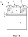
- FIG. 14 is a cross-sectional side view of a portion of an illustrative pixel array of the type shown in FIG. 13 .
- FIG. 15 is a flow chart of illustrative method steps that may be involved in forming a pixel array having a color filter layer with colored elements, clear elements, and color filter container structures.
- FIG. 16 is a block diagram of an illustrative processor system employing the embodiments of FIGS. 1-15 in accordance with an embodiment of the present invention.
- Electronic devices such as digital cameras, computers, cellular telephones, and other electronic devices may include image sensors that gather incoming light to capture an image.
- the image sensors may include arrays of image pixels.
- the pixels in the image sensors may include photosensitive elements such as photodiodes that convert the incoming light into image signals.
- Image sensors may have any number of pixels (e.g., hundreds or thousands or more).
- a typical image sensor may, for example, have hundreds of thousands or millions of pixels (e.g., megapixels).
- Image sensors may include control circuitry such as circuitry for operating the image pixels and readout circuitry for reading out image signals corresponding to the electric charge generated by the photosensitive elements.
- FIG. 1 is a diagram of an illustrative imaging system such as an electronic device that uses an image sensor to capture images.
- Electronic device 10 of FIG. 1 may be a portable electronic device such as a camera, a cellular telephone, a tablet computer, a webcam, a video camera, a video surveillance system, an automotive imaging system, a video gaming system with imaging capabilities, or any other desired imaging system or device that captures digital image data.
- Camera module 12 may be used to convert incoming light into digital image data.
- Camera 12 may include one or more lenses 14 and one or more corresponding image sensors 16 .
- Lenses 14 may include fixed and/or adjustable lenses and may include microlenses formed on an imaging surface of image sensor 16 .
- Image sensor 16 may include circuitry for converting analog pixel data into corresponding digital image data to be provided to storage and processing circuitry 18 .
- camera module 12 may be provided with an array of lenses 14 and an array of corresponding image sensors 16 .
- Storage and processing circuitry 18 may include one or more integrated circuits (e.g., image processing circuits, microprocessors, storage devices such as random-access memory and non-volatile memory, etc.) and may be implemented using components that are separate from camera module 12 and/or that form part of camera module 12 (e.g., circuits that form part of an integrated circuit that includes image sensors 16 or an integrated circuit within module 12 that is associated with image sensors 16 ).
- Image data that has been captured by camera module 12 may be processed and stored using processing circuitry 18 (e.g., using an image processing engine on processing circuitry 18 , using an imaging mode selection engine on processing circuitry 18 , etc.).
- Processed image data may, if desired, be provided to external equipment (e.g., a computer, external display, or other device) using wired and/or wireless communications paths coupled to processing circuitry 18 .
- image sensor 16 may include a pixel array 20 containing image sensor pixels 22 arranged in rows and columns (sometimes referred to herein as image pixels or pixels) and control and processing circuitry 24 (which may include, for example, image signal processing circuitry).
- Array 20 may contain, for example, hundreds or thousands of rows and columns of image sensor pixels 22 .
- Control circuitry 24 may be coupled to row control circuitry 26 and image readout circuitry 28 (sometimes referred to as column control circuitry, readout circuitry, processing circuitry, or column decoder circuitry).
- Row control circuitry 26 may receive row addresses from control circuitry 24 and supply corresponding row control signals such as reset, row-select, charge transfer, dual conversion gain, and readout control signals to pixels 22 over row control paths 30 .
- One or more conductive lines such as column lines 32 may be coupled to each column of pixels 22 in array 20 .
- Column lines 32 may be used for reading out image signals from pixels 22 and for supplying bias signals (e.g., bias currents or bias voltages) to pixels 22 .
- bias signals e.g., bias currents or bias voltages
- a pixel row in array 20 may be selected using row control circuitry 26 and image signals generated by image pixels 22 in that pixel row can be read out along column lines 32 .
- Image readout circuitry 28 may receive image signals (e.g., analog pixel values generated by pixels 22 ) over column lines 32 .
- Image readout circuitry 28 may include sample-and-hold circuitry for sampling and temporarily storing image signals read out from array 20 , amplifier circuitry, analog-to-digital conversion (ADC) circuitry, bias circuitry, column memory, latch circuitry for selectively enabling or disabling the column circuitry, or other circuitry that is coupled to one or more columns of pixels in array 20 for operating pixels 22 and for reading out image signals from pixels 22 .
- ADC circuitry in readout circuitry 28 may convert analog pixel values received from array 20 into corresponding digital pixel values (sometimes referred to as digital image data or digital pixel data).
- Image readout circuitry 28 may supply digital pixel data to control and processing circuitry 24 and/or processor 18 ( FIG. 1 ) over path 25 for pixels in one or more pixel columns.
- a color filter array may be formed over photosensitive regions in array 20 so that a desired color filter element in the color filter array is formed over an upper surface of the photosensitive region of an associated pixel 22 .
- a microlens may be formed over an upper surface of the color filter array to focus incoming light onto the photosensitive region associated with that pixel 22 .
- Incoming light may be focused onto the photosensitive region by the microlens and may pass through the color filter element so that only light of a corresponding color is captured at the photosensitive region.
- an antireflection coating may be formed on the microlens.
- pixels 22 in array 20 of FIG. 2 may be provided with an array of color filter elements that each pass one or more colors of light. All or some of pixels 22 may be provided with a color filter element.
- Color filter elements for pixels 22 may be red color filter elements (e.g., photoresist material that passes red light while reflecting and/or absorbing other colors of light), blue color filter elements (e.g., photoresist material that passes blue light while reflecting and/or absorbing other colors of light), and/or green color filter elements (e.g., photoresist material that passes green light while reflecting and/or absorbing other colors of light).
- some pixels 22 in array 20 may be provided with transparent material that passes light throughout the visible spectrum (e.g., red, green, and blue light).
- This transparent material may take the place of the color filter elements in these pixels, but may not filter light based on wavelength as the other color filter elements do. Due to their location in the array with the other color filter elements, however, this transparent material may be referred to as a clear color filter element, a transparent color filter element, or a clear element. Pixels that include this transparent material in place of a red, green, blue, or other wavelength-selective color filter may be referred to as clear pixels.
- Color filter elements may also be configured to filter light that is outside the visible human spectrum.
- color filter elements may be configured to filter ultraviolet or infrared light (e.g., a color filter element may only allow infrared light or ultraviolet light to reach the photodiode).
- Color filter elements may configure image pixel 22 to only detect light of a certain wavelength or range of wavelengths (sometimes referred to herein as a wavelength band) and may be configured to allow multiple wavelengths of light to pass while blocking light of certain other wavelengths (for example, light having a wavelength that corresponds to a certain visible color and/or an infrared or ultraviolet wavelength).
- Color filter elements that pass two or more colors of light are sometimes referred to herein as “broadband” filter elements.
- yellow color filter elements that are configured to pass red and green light may be referred to herein as broadband filter elements or broadband color filter elements.
- Magenta color filter elements that are configured to pass red and blue light may be also be referred to herein as broadband filter elements or broadband color filter elements.
- Clear color filter elements that are configured to pass red, green, blue, and other wavelengths of visible or non-visible light may also be referred to herein as broadband filter elements or broadband color filter elements.
- image pixels that include a broadband color filter element e.g., a yellow, magenta, or clear color filter element
- broadband pixels e.g., a yellow, magenta, or clear color filter element
- Image signals generated by broadband image pixels may sometimes be referred to herein as broadband image signals.
- Broadband image pixels may have a natural sensitivity defined by the material that forms the broadband color filter element and/or the material that forms the image sensor pixel (e.g., silicon). In another suitable arrangement, broadband image pixels may be formed without any color filter elements.
- broadband image pixels may, if desired, be adjusted for better color reproduction and/or noise characteristics through use of light absorbers such as pigments.
- colored pixel may be used herein to refer to image pixels that are primarily sensitive to one color of light (e.g., red light, blue light, green light, or light of any other suitable color). Colored pixels may sometimes be referred to herein as narrowband image pixels because the colored pixels have a narrower spectral response than the broadband image pixels.
- narrowband pixels and/or broadband pixels that are not configured to be sensitive to infrared light may be provided with color filters incorporating absorbers of NIR radiation.
- Color filters that block near-infrared light may minimize the impact of infrared light on color reproduction in illuminants containing both visible and infrared radiation.
- image sensor pixels such as the image pixels in array 20 may be provided with a color filter array which allows a single image sensor to sample red, green, and blue (RGB) light using corresponding red, green, and blue image sensor pixels arranged in a Bayer mosaic pattern.
- the Bayer mosaic pattern consists of a repeating unit cell of two-by-two image pixels, with two green image pixels diagonally opposite one another and adjacent to a red image pixel diagonally opposite to a blue image pixel.
- SNR signal to noise ratio
- the green pixels in a Bayer pattern are replaced by broadband image pixels having broadband color filter elements (e.g., clear color filter elements).
- broadband color filter elements e.g., clear color filter elements.
- a color filter layer may include color filter housing structures (sometimes referred to herein as color filter container structures, light-blocking structures, an in-pixel grid, or light containment structures) in which the color filter elements are formed.
- Color filter housing structures may include a grid of material that forms an array of openings in which color filter elements are deposited (e.g., the color filter elements fill the holes).
- An array of color filter elements that are contained within such housing structures are sometimes referred to as a color filter array-in-a-box (sometimes abbreviated as “CFA-in-a-box” or “CIAB”).
- Color filter housing structures may have light-blocking or light-reflecting properties that prevent light that is incident upon one pixel from reaching an adjacent pixel as the light passes through a color filter element. In this way, color filter housing structures may offer improved light guiding capabilities for directing light to desired image sensor pixels.
- FIG. 3 is a top view of an illustrative portion of an array 20 of image pixels 22 having a CIAB arrangement of the type described above.
- a grid of color filter container material 50 forms an array of openings 54 .
- the color filter elements of individual pixels 22 are formed in the openings 54 .
- array 20 includes some pixels 22 having color filter elements 34 (e.g., red, green, and/or blue color filter elements) and some pixels 22 having clear elements 36 .
- color filter elements 34 and clear elements 36 in FIG. 3 is merely illustrative. In general, color filter elements 34 and clear elements 36 may be arranged in any suitable pattern. Color filter elements 34 of different colors may also be arranged in a variety of suitable patterns (e.g., a Bayer mosaic pattern, a modified Bayer mosaic pattern in which green color filters are replaced with clear filter elements, etc.).
- color filter elements 34 may be formed of red, green, blue, cyan, yellow, magenta, or other colored photoresists that are patterned using photolithography techniques.
- organic materials having refractive indices of between 1.6 and 1.8 may be used for forming red, green, blue, cyan, yellow, magenta, or other colors of color filter elements.
- Clear elements 36 may be formed of a transparent dielectric material such as silicon dioxide (SiO 2 ), silicon nitride (Si 3 N 4 ), or silicon oxynitride (SiON), as examples.
- clear dielectric elements 36 may be formed of dielectric materials having indices of refraction that are higher than those of the photoresist materials used to form colored elements 34 (e.g., clear dielectric elements 36 may be formed from dielectric materials having an index of refraction between 1.8 and 2.2).
- FIG. 4 is an illustrative cross-sectional side view of the portion of array 20 in FIG. 3 taken along line A-A.
- pixel array 20 may include a layer of silicon 38 (e.g., a layer of epitaxial silicon) in which photodiodes for the pixels 22 are formed.
- Dielectric layers such as dielectric layer 40 (e.g., a high-k dielectric such as hafnium oxide or tantalum pentoxide), dielectric layer 42 (e.g., an oxide layer), and dielectric layer 44 (e.g., a nitride layer) may be formed over silicon layer 38 .
- Color filter container structures 50 are formed on the dielectric layers and form openings 54 in which color elements 34 and clear elements 36 are formed.
- Each pixel 22 may be provided with a microlens 46 .
- Microlenses 46 may be formed of a transparent organic material having a refractive index of approximately 1.4-1.6. In the illustrative example of FIG. 4 , microlenses 46 are formed directly on color filter elements 34 and clear elements 36 without any intervening layers.
- An antireflective coating 48 may be provided over the microlenses 46 .
- Antireflective coating 48 may be formed of a transparent dielectric material (e.g., silicon dioxide having a refractive index of about 1.4-1.5).
- container structures 50 may be formed of opaque material.
- container material 50 may be an opaque organic material, an opaque metal material, an opaque metalorganic material, or a combination (composite) of metal material and dielectric material such as oxide (sometimes referred to herein as a composite grid).
- container material 50 of FIG. 4 may be black, white, red, green, blue, or some other opaque color.
- Opaque container material of the type described in connection with FIG. 4 may be formed using spin-on techniques, chemical vapor deposition, physical vapor deposition, or other deposition processes.
- CMP Chemical-mechanical planarization
- microlenses 46 are formed directly on the upper surfaces of color filter elements 34 , clear elements 36 , and container structures 50 .
- a planarization layer 52 may be formed between the color filter layer in which elements 34 and 36 are formed, and the microlens layer in which microlenses 46 are formed. Planarization layer 52 may help planarize the surface of color filter elements 34 , clear elements 36 , and container structures 50 , thereby providing a planar surface on which microlenses 46 may be formed.
- Planarization layer 52 may be formed of transparent organic material having a refractive index of approximately 1.4-1.6.
- color filter elements 34 , clear elements 36 , and container structures 50 may form a planar surface on which microlenses 46 may be formed without the presence of planarization layer 52 . In this way, planarization layer 52 may be optional.
- planarization layer 52 itself may be used to form container structures 50 .
- FIG. 6 An illustrative example of such an arrangement is shown in FIG. 6 .
- planarization layer 52 is formed of transparent material (e.g., transparent organic material) to allow light to pass to the photodiodes in silicon layer 38 , there may be a relatively large index of refraction difference between the material of planarization layer 52 and the elements in the color filter layer. Accordingly, there may be a relatively large index of refraction difference between color filter container structures 50 formed from planarization layer 52 and colored elements 34 .
- clear elements 36 are formed of transparent materials having high indices of refraction, there may also be a high index of refraction difference between color filter container structures 50 formed from planarization layer 52 and clear elements 36 , despite the fact that both of these structures are transparent. These large index of refraction differences may prevent light from passing from the clear element 36 or colored element 34 of one pixel into the filter element of an adjacent pixel, thereby reducing cross-talk between pixels 22 .
- planarization layer 52 as the color filter container material 50 , the need for an additional layer of material for the color filter container structures (and the manufacturing steps associated with such a layer) may be avoided.
- layer 52 is a planarization layer formed of, for example, transparent organic material. This, however, is merely illustrative. If desired, layer 52 may be formed from a conductive, transparent dielectric material such as indium tin oxide (ITO). In arrangements in which layer 52 extends between filter elements 34 and 36 to form container structures 50 , the container structures 50 may be made to be conductive. If desired, clear elements 36 may also be formed from indium tin oxide, both in arrangements in which container structures 50 are formed from indium tin oxide, and in arrangements in which container structures 50 are formed from other materials (or omitted entirely).
- ITO indium tin oxide
- container structures 50 and/or clear elements 36 By forming container structures 50 and/or clear elements 36 from indium tin oxide, it may be possible to ground the container structures 50 through a ground bond pad. By grounding container structures 50 , electrical charge that accumulates during fabrication of image sensor 16 may be discharged. This may reduce dark current (e.g., plasma-induced dark current) generated by pixels 22 as a result of image sensor fabrication processes, thereby increasing the signal-to-noise ratio of the sensor 16 .
- dark current e.g., plasma-induced dark current
- material from microlenses 46 may be used to form container structures 50 .
- FIG. 7 An illustrative example of such an arrangement is shown in FIG. 7 .
- microlenses 46 are formed of transparent material (e.g., transparent organic material) to direct light to the photodiodes in silicon layer 38 , there may be a relatively large index of refraction difference between the material of microlenses 46 and the elements in the color filter layer. Accordingly, there may be a relatively large index of refraction difference between color filter container structures 50 formed from material from microlenses 46 and colored elements 34 .
- clear elements 36 are formed of transparent materials having high indices of refraction, there may also be a high index of refraction difference between color filter container structures 50 formed from microlens material 46 and clear elements 36 , despite the fact that both of these structures are transparent. These large index of refraction differences may prevent light from passing from the clear element 36 or colored element 34 of one pixel into the filter element of an adjacent pixel, thereby reducing cross-talk between pixels 22 .
- the material of microlenses 46 as the color filter container material 50 , the need for an additional layer of material for the color filter container structures (and the manufacturing steps associated with such a layer) may be avoided.
- antireflective coating 48 may be used to form container structures 50 .
- FIG. 8 An illustrative example of such an arrangement is shown in FIG. 8 .
- antireflective coating 48 is formed of transparent material (e.g., transparent dielectric material such as silicon dioxide) to allow light to reach photodiodes in silicon layer 38 , there may be a relatively large index of refraction difference between antireflective coating 48 and the elements in the color filter layer. Accordingly, there may be a relatively large index of refraction difference between color filter container structures 50 formed from material from antireflective layer 48 and colored elements 34 .
- clear elements 36 are formed of transparent materials having high indices of refraction, there may also be a high index of refraction difference between color filter container structures 50 formed from antireflective layer 48 and clear elements 36 , despite the fact that both of these structures are transparent. These large index of refraction differences may prevent light from passing from the clear element 36 or colored element 34 of one pixel into the filter element of an adjacent pixel, thereby reducing cross-talk between pixels 22 .
- the material of antireflection layer 48 as the color filter container material 50 , the need for an additional layer of material for the color filter container structures (and the manufacturing steps associated with such a layer) may be avoided.
- the gaps between color filter elements 34 and clear elements 36 may be filled with air rather than opaque or transparent material of the type described above in connection with FIGS. 1-8 .
- Illustrative examples of this type of arrangement are shown in FIGS. 9 and 10 .
- microlenses 46 are formed such that they close off the tops of the air gaps between color filter elements 34 and clear elements 36 .
- antireflective coating 48 is deposited such that the dielectric material of the antireflective coating 48 closes off the tops of the gaps between color filter elements 34 and clear elements 36 . Due to the deposition process used to form antireflective coating 48 , some of the dielectric material may be deposited onto dielectric layer 44 between elements 34 and 36 , as shown in FIG. 10 .
- color filter element container structures 50 are omitted from pixel array 20 .
- the air that replaces the container structures 50 is generally transparent, there may still be a relatively large index of refraction difference between the air and the elements in the color filter layer. Accordingly, there may be a relatively large index of refraction difference between the air and colored elements 34 , as well as between the air and clear elements 36 . These high index of refraction differences may prevent light from passing from the clear element 36 or colored element 34 of one pixel into the filter element of an adjacent pixel, thereby reducing cross-talk between pixels 22 .
- color filter container structures 50 By not forming color filter container structures 50 (and instead utilizing the high refractive index difference between the elements 34 / 36 and air to prevent crosstalk), the need for an additional layer of material for the color filter container structures (and the manufacturing steps associated with such a layer) may be avoided.
- clear elements 36 and color filter container structures 50 may be formed of the same material (e.g., as a single continuous structure).
- a top view of an illustrative pixel array 20 having this type of arrangement is shown in FIG. 11 .
- colored elements 34 are separated from each other by color filter container structures 50 (i.e., colored filter elements 34 are formed in the openings 54 of container structures 50 ).
- the material of color filter container structures 50 may fill the locations in array 20 at which clear elements 36 are to be formed (illustrated by the dashed line showing the location of clear element 36 among other portions of the same material that forms container structures 50 ).
- the material of clear elements 36 may extend between colored elements 34 to form container structures 50 having openings 54 in which colored elements 34 are formed.
- FIG. 12 is a cross-sectional side view of a pixel array 20 taken along line B-B in FIG. 11 .
- the clear material of clear element 36 may take up the entire gap between colored elements 34 .
- the index of refraction difference between clear element 36 and the colored element 34 (which abut each other in this case) may be sufficiently large so as to prevent light that is incident at the junction between the two materials from passing from element 36 to element 34 (or vice-versa).
- the clear material of clear element 36 may also extend between adjacent colored elements 34 between which there is no clear element 36 , instead forming a portion of the grid of color filter container structures 50 . Where the clear material of elements 36 forms the container structures 50 , the index of refraction difference between the container structures 50 and the colored elements 34 may be sufficiently large so as to prevent light from prematurely exiting one colored element 34 and entering another adjacent pixel 22 .
- array 20 may be formed without container structures 50 or air gaps between elements 34 and 36 such that some or all of the elements in the array abut each other.
- FIG. 13 A top view of an illustrative example of this type of arrangement is shown in FIG. 13 . As shown in FIG. 13 , the edges of each filter element abut the edges of the filter elements adjacent to it. There are no gaps between the filter elements 34 and 36 in the example of FIG. 13 , so neither container structures 50 of the type shown in FIGS. 3-8, 11, and 12 , nor air gaps of the type shown in FIGS. 9 and 10 , are present.
- FIG. 14 is a cross-sectional side view of a pixel array 20 taken along line C-C in FIG. 13 .
- the vertical sidewalls of clear element 36 directly contact the vertical sidewalls of adjacent elements 34 .
- the index of refraction difference between clear element 36 and the colored element 34 may be sufficiently large so as to prevent light that is incident at the junction between the two materials from passing from element 36 to element 34 (or vice-versa). Due to the large index of refraction difference between the material that forms clear element 36 and the material that forms colored elements 34 , a grid of light-blocking material (e.g., container structures 50 ) may be omitted while still minimizing crosstalk between adjacent pixels.
- a grid of light-blocking material e.g., container structures 50
- the arrangements described above may be incorporated in backside illuminated image sensors in which metal routing structures for the pixels 22 are beneath the photodiodes in epitaxial silicon layer 38 . In this type of arrangement, light does not pass through the metal routing structures before reaching the photodiodes.
- the arrangements described above may be incorporated in a frontside illuminate image sensor in which metal routing structures for the pixels 22 are between the photodiodes in epitaxial silicon layer 38 and the microlenses 46 . In this type of arrangement, light does pass through the metal routing structures before reaching the photodiodes.
- the pixel array 20 is described as including both colored elements 34 and clear elements 36 . This, however, is merely illustrative. If desired, pixel array 20 may be provided exclusively with clear elements 36 (i.e., may be free of colored elements 34 ) in order to provide a monochromatic image sensor 16 . In arrangements in which image sensor 16 is monochromatic, container structures 50 may be provided as described above in connection with any of the examples in FIGS. 3-8, 11, and 12 , or may be omitted as described above in connection with any of the examples of FIGS. 9, 10, 13, and 14 .
- a single opening 54 in container structures 50 may be large enough to overlap multiple photodiodes of multiple adjacent pixels.
- the clear dielectric material or colored photoresist for the multiple pixels may fill these larger openings in container structures 50 .
- single clear or colored elements that overlap photodiodes for multiple pixels may also be implemented in arrangements that do not include container structures 50 (e.g., arrangements of the type shown and described in connection with FIGS. 13 and 14 ).
- transparent dielectric material may be deposited (e.g., over dielectric layers 40 , 42 , and/or 44 ).
- the transparent dielectric material may be patterned (e.g., using photolithography techniques).
- the patterned transparent dielectric material may be etched to form clear elements 36 .
- the colored photoresist may be patterned using photolithography techniques to form the color filter elements 34 .
- light blocking material may be deposited to form color filter container structures 50 .
- the light-blocking material may be opaque organic material, transparent organic material used to form planarization layer 52 or microlenses 46 , or transparent dielectric material used to form antireflection coating 48 .
- step 110 may be performed simultaneously with steps 100 , 102 , and 104 (i.e., before steps 106 and 108 ).
- step 110 may be omitted (e.g., step 110 may be optional).
- steps 106 and 108 may be omitted (e.g., steps 106 and 108 may be optional).
- FIG. 16 shows in simplified form a typical processor system 1800 , such as a digital camera, which includes an imaging device 2000 (e.g., an imaging device 2000 such as image sensor 16 employing image pixel array 20 of the type shown in FIGS. 1-14 having clear elements 36 formed of dielectric material).
- the processor system 1800 is exemplary of a system having digital circuits that could include imaging device 2000 . Without being limiting, such a system could include a computer system, still or video camera system, scanner, machine vision, vehicle navigation, video phone, surveillance system, auto focus system, star tracker system, motion detection system, image stabilization system, and other systems employing an imaging device.
- the processor system 1800 generally includes a lens 1896 for focusing an image on pixel array 20 of device 2000 when a shutter release button 1897 is pressed, central processing unit (CPU) 1895 , such as a microprocessor which controls camera and one or more image flow functions, which communicates with one or more input/output (I/O) devices 1891 over a bus 1893 .
- Imaging device 2000 also communicates with the CPU 1895 over bus 1893 .
- the system 1800 also includes random access memory (RAM) 1892 and can include removable memory 1894 , such as flash memory, which also communicates with CPU 1895 over the bus 1893 .
- Imaging device 2000 may be combined with the CPU, with or without memory storage on a single integrated circuit or on a different chip.
- bus 1893 is illustrated as a single bus, it may be one or more busses or bridges or other communication paths used to interconnect the system components.
- a pixel array may include an array of photodiodes and a color filter layer that overlaps the array of photodiodes.
- the color filter layer may include a grid of color filter container material that forms an array of openings over the array of photodiodes, organic color filter material that fills a first set of the openings, and transparent dielectric material that fills a second set of the openings.
- the transparent dielectric material may form the grid of color filter container material such that the second set of openings is defined by blocks of transparent dielectric material that are integrally formed with the grid of color filter container material, rather than by gaps in the grid of color filter container material.
- the transparent dielectric material may include silicon nitride.
- the grid of color filter container material may be opaque.
- the grid of color filter container material may include transparent organic material.
- the organic color filter material may have a first index of refraction, and the transparent dielectric material may have a second index of refraction that is greater than the first index of refraction.
- the grid of color filter container material may include an additional transparent dielectric material that has a third index of refraction that is different than the second index of refraction.
- Each of the first color filter elements and the second color filter elements may be surrounded by the clear dielectric material.
- a grid of material that is separate from the first color filter elements, the second color filter elements, and the clear dielectric material may form an array of openings in which the first color filter elements, the second color filter elements, and the clear dielectric material are formed.
- the grid of material may be opaque.
- the pixel array may include an array of microlenses formed from transparent organic material that overlaps the color filter layer and an antireflective coating formed on the array of microlenses.
- the transparent organic material that forms the microlenses may also form the grid of material.
- the antireflective coating may form the grid of material.
- the array of microlenses may be formed directly on the first color filter elements, the second color filter elements, and the clear dielectric material.
- the pixel array may include a planarization layer interposed between the color filter layer and the array of microlenses.
- the planarization layer may form the grid of material.
- the planarization layer and the grid of material may be formed from indium tin oxide.
Abstract
Description
Claims (13)
Priority Applications (2)
| Application Number | Priority Date | Filing Date | Title |
|---|---|---|---|
| US15/787,959 US10510787B2 (en) | 2017-10-19 | 2017-10-19 | Structures and methods of creating clear pixels |
| CN201821675901.0U CN208970511U (en) | 2017-10-19 | 2018-10-16 | Pixel array and color-filter layer for imaging sensor |
Applications Claiming Priority (1)
| Application Number | Priority Date | Filing Date | Title |
|---|---|---|---|
| US15/787,959 US10510787B2 (en) | 2017-10-19 | 2017-10-19 | Structures and methods of creating clear pixels |
Publications (2)
| Publication Number | Publication Date |
|---|---|
| US20190123083A1 US20190123083A1 (en) | 2019-04-25 |
| US10510787B2 true US10510787B2 (en) | 2019-12-17 |
Family
ID=66169563
Family Applications (1)
| Application Number | Title | Priority Date | Filing Date |
|---|---|---|---|
| US15/787,959 Active US10510787B2 (en) | 2017-10-19 | 2017-10-19 | Structures and methods of creating clear pixels |
Country Status (2)
| Country | Link |
|---|---|
| US (1) | US10510787B2 (en) |
| CN (1) | CN208970511U (en) |
Families Citing this family (8)
| Publication number | Priority date | Publication date | Assignee | Title |
|---|---|---|---|---|
| KR102506837B1 (en) * | 2017-11-20 | 2023-03-06 | 삼성전자주식회사 | Image sensor and method for fabricating the same |
| KR102498582B1 (en) * | 2018-02-26 | 2023-02-14 | 에스케이하이닉스 주식회사 | Image Sensor Including Partition Patterns |
| CN110277419B (en) * | 2019-06-28 | 2022-02-08 | 德淮半导体有限公司 | Image sensor and forming method thereof |
| KR20210048059A (en) | 2019-10-23 | 2021-05-03 | 삼성전자주식회사 | Image sensor |
| KR20210056754A (en) * | 2019-11-11 | 2021-05-20 | 에스케이하이닉스 주식회사 | Image Sensor |
| KR20210070800A (en) * | 2019-12-05 | 2021-06-15 | 삼성전자주식회사 | Image sensors |
| US20210197506A1 (en) * | 2019-12-31 | 2021-07-01 | Semiconductor Components Industries, Llc | Microlens device and related methods |
| EP4109895A4 (en) * | 2020-02-19 | 2023-07-26 | Sony Group Corporation | Image processing method and sensor device |
Citations (17)
| Publication number | Priority date | Publication date | Assignee | Title |
|---|---|---|---|---|
| US5889277A (en) * | 1995-11-20 | 1999-03-30 | Eastman Kodak Company | Planar color filter array for CCDs with embedded color filter elements |
| US20090224347A1 (en) * | 2008-03-04 | 2009-09-10 | Kim Sung-Kwan | Image sensor and method of manufacturing the same |
| US7955764B2 (en) | 2006-04-07 | 2011-06-07 | Micron Technology, Inc. | Methods to make sidewall light shields for color filter array |
| US20120019695A1 (en) | 2010-07-26 | 2012-01-26 | Omnivision Technologies, Inc. | Image sensor having dark sidewalls between color filters to reduce optical crosstalk |
| US20120086093A1 (en) * | 2010-10-07 | 2012-04-12 | Sony Corporation | Solid-state imaging device, method of manufacturing solid-state imaging device, and electronic apparatus |
| US20140098332A1 (en) * | 2012-10-10 | 2014-04-10 | Apple Inc. | Displays With Logos and Alignment Marks |
| US20140210032A1 (en) * | 2010-07-15 | 2014-07-31 | Sony Corporation | Solid-state imaging device, method for manufacturing solid-state imaging device, and electronic apparatus |
| US20140210028A1 (en) | 2013-01-30 | 2014-07-31 | Omnivision Technologies, Inc. | Color filter including clear pixel and hard mask |
| US20150048467A1 (en) | 2013-08-15 | 2015-02-19 | Taiwan Semiconductor Manufacturing Company, Ltd. | Structure of Dielectric Grid with a Metal Pillar for Semiconductor Device |
| US9013612B2 (en) * | 2010-08-20 | 2015-04-21 | Semiconductor Components Industries, Llc | Image sensors with antireflective layers |
| US20160054173A1 (en) * | 2014-08-21 | 2016-02-25 | Samsung Electronics Co., Ltd. | Image sensor having improved light utilization efficiency and method of manufacturing the same |
| US20160148970A1 (en) * | 2014-11-26 | 2016-05-26 | Taiwan Semiconductor Manufacturing Company Ltd. | Image sensing device and manufacturing method thereof |
| US20160276396A1 (en) * | 2013-12-12 | 2016-09-22 | Sony Corporation | Solid state imaging device, manufacturing method of the same, and electronic equipment |
| US20170077160A1 (en) * | 2012-02-24 | 2017-03-16 | Canon Kabushiki Kaisha | Solid-state image pickup device and image pickup system |
| US20170170220A1 (en) * | 2015-12-14 | 2017-06-15 | Samsung Electronics Co., Ltd. | Image sensor having hybrid color filter |
| US20170301718A1 (en) * | 2016-04-13 | 2017-10-19 | Taiwan Semiconductor Manufacturing Co., Ltd. | Full-pdaf (phase detection autofocus) cmos image sensor structures |
| US20180076247A1 (en) * | 2016-09-13 | 2018-03-15 | Omnivision Technologies, Inc. | Backside-Illuminated Color Image Sensors With Crosstalk-Suppressing Color Filter Array |
-
2017
- 2017-10-19 US US15/787,959 patent/US10510787B2/en active Active
-
2018
- 2018-10-16 CN CN201821675901.0U patent/CN208970511U/en active Active
Patent Citations (17)
| Publication number | Priority date | Publication date | Assignee | Title |
|---|---|---|---|---|
| US5889277A (en) * | 1995-11-20 | 1999-03-30 | Eastman Kodak Company | Planar color filter array for CCDs with embedded color filter elements |
| US7955764B2 (en) | 2006-04-07 | 2011-06-07 | Micron Technology, Inc. | Methods to make sidewall light shields for color filter array |
| US20090224347A1 (en) * | 2008-03-04 | 2009-09-10 | Kim Sung-Kwan | Image sensor and method of manufacturing the same |
| US20140210032A1 (en) * | 2010-07-15 | 2014-07-31 | Sony Corporation | Solid-state imaging device, method for manufacturing solid-state imaging device, and electronic apparatus |
| US20120019695A1 (en) | 2010-07-26 | 2012-01-26 | Omnivision Technologies, Inc. | Image sensor having dark sidewalls between color filters to reduce optical crosstalk |
| US9013612B2 (en) * | 2010-08-20 | 2015-04-21 | Semiconductor Components Industries, Llc | Image sensors with antireflective layers |
| US20120086093A1 (en) * | 2010-10-07 | 2012-04-12 | Sony Corporation | Solid-state imaging device, method of manufacturing solid-state imaging device, and electronic apparatus |
| US20170077160A1 (en) * | 2012-02-24 | 2017-03-16 | Canon Kabushiki Kaisha | Solid-state image pickup device and image pickup system |
| US20140098332A1 (en) * | 2012-10-10 | 2014-04-10 | Apple Inc. | Displays With Logos and Alignment Marks |
| US20140210028A1 (en) | 2013-01-30 | 2014-07-31 | Omnivision Technologies, Inc. | Color filter including clear pixel and hard mask |
| US20150048467A1 (en) | 2013-08-15 | 2015-02-19 | Taiwan Semiconductor Manufacturing Company, Ltd. | Structure of Dielectric Grid with a Metal Pillar for Semiconductor Device |
| US20160276396A1 (en) * | 2013-12-12 | 2016-09-22 | Sony Corporation | Solid state imaging device, manufacturing method of the same, and electronic equipment |
| US20160054173A1 (en) * | 2014-08-21 | 2016-02-25 | Samsung Electronics Co., Ltd. | Image sensor having improved light utilization efficiency and method of manufacturing the same |
| US20160148970A1 (en) * | 2014-11-26 | 2016-05-26 | Taiwan Semiconductor Manufacturing Company Ltd. | Image sensing device and manufacturing method thereof |
| US20170170220A1 (en) * | 2015-12-14 | 2017-06-15 | Samsung Electronics Co., Ltd. | Image sensor having hybrid color filter |
| US20170301718A1 (en) * | 2016-04-13 | 2017-10-19 | Taiwan Semiconductor Manufacturing Co., Ltd. | Full-pdaf (phase detection autofocus) cmos image sensor structures |
| US20180076247A1 (en) * | 2016-09-13 | 2018-03-15 | Omnivision Technologies, Inc. | Backside-Illuminated Color Image Sensors With Crosstalk-Suppressing Color Filter Array |
Also Published As
| Publication number | Publication date |
|---|---|
| CN208970511U (en) | 2019-06-11 |
| US20190123083A1 (en) | 2019-04-25 |
Similar Documents
| Publication | Publication Date | Title |
|---|---|---|
| US10510787B2 (en) | Structures and methods of creating clear pixels | |
| US10297629B2 (en) | Image sensors with in-pixel lens arrays | |
| US9699393B2 (en) | Imaging systems for infrared and visible imaging with patterned infrared cutoff filters | |
| US10165211B1 (en) | Image sensors with optically black pixels | |
| KR102568441B1 (en) | Solid-state imaging element, production method thereof, and electronic device | |
| CN106068563B (en) | Solid-state imaging device, method of manufacturing solid-state imaging device, and electronic apparatus | |
| US9219090B2 (en) | Solid-state image capturing device and electronic device | |
| KR101358587B1 (en) | Solid-state image sensor and imaging system | |
| US9373732B2 (en) | Image sensors with reflective optical cavity pixels | |
| US9041081B2 (en) | Image sensors having buried light shields with antireflective coating | |
| US8471311B2 (en) | Anti-reflective image sensor | |
| US7799491B2 (en) | Color filter array and imaging device containing such color filter array and method of fabrication | |
| US20130293751A1 (en) | Imaging systems with separated color filter elements | |
| US8878969B2 (en) | Imaging systems with color filter barriers | |
| US9172892B2 (en) | Imaging systems with image pixels having varying light collecting areas | |
| US8890221B2 (en) | Backside illuminated image sensor pixels with dark field microlenses | |
| WO2008130846A9 (en) | Methods to make sidewall light shields for color filter array | |
| US9786702B2 (en) | Backside illuminated image sensors having buried light shields with absorptive antireflective coating | |
| KR102223515B1 (en) | Solid-state imaging device and electronic device | |
| US8077230B2 (en) | Methods and apparatus for reducing color material related defects in imagers | |
| US9947705B1 (en) | Image sensors with infrared-blocking layers | |
| US20210280624A1 (en) | Imaging systems with improved microlenses for enhanced near-infrared detection |
Legal Events
| Date | Code | Title | Description |
|---|---|---|---|
| AS | Assignment |
Owner name: SEMICONDUCTOR COMPONENTS INDUSTRIES, LLC, ARIZONA Free format text: ASSIGNMENT OF ASSIGNORS INTEREST;ASSIGNORS:BORTHAKUR, SWARNAL;CHAPMAN, NATHAN WAYNE;VAARTSTRA, BRIAN ANTHONY;SIGNING DATES FROM 20171016 TO 20171018;REEL/FRAME:043902/0368 |
|
| FEPP | Fee payment procedure |
Free format text: ENTITY STATUS SET TO UNDISCOUNTED (ORIGINAL EVENT CODE: BIG.); ENTITY STATUS OF PATENT OWNER: LARGE ENTITY |
|
| AS | Assignment |
Owner name: DEUTSCHE BANK AG NEW YORK BRANCH, AS COLLATERAL AG Free format text: PATENT SECURITY AGREEMENT;ASSIGNORS:SEMICONDUCTOR COMPONENTS INDUSTRIES, LLC;FAIRCHILD SEMICONDUCTOR CORPORATION;REEL/FRAME:046530/0494 Effective date: 20180206 Owner name: DEUTSCHE BANK AG NEW YORK BRANCH, AS COLLATERAL AGENT, NEW YORK Free format text: PATENT SECURITY AGREEMENT;ASSIGNORS:SEMICONDUCTOR COMPONENTS INDUSTRIES, LLC;FAIRCHILD SEMICONDUCTOR CORPORATION;REEL/FRAME:046530/0494 Effective date: 20180206 |
|
| STPP | Information on status: patent application and granting procedure in general |
Free format text: NON FINAL ACTION MAILED |
|
| STPP | Information on status: patent application and granting procedure in general |
Free format text: RESPONSE TO NON-FINAL OFFICE ACTION ENTERED AND FORWARDED TO EXAMINER |
|
| STPP | Information on status: patent application and granting procedure in general |
Free format text: NOTICE OF ALLOWANCE MAILED -- APPLICATION RECEIVED IN OFFICE OF PUBLICATIONS |
|
| STPP | Information on status: patent application and granting procedure in general |
Free format text: PUBLICATIONS -- ISSUE FEE PAYMENT VERIFIED |
|
| STCF | Information on status: patent grant |
Free format text: PATENTED CASE |
|
| MAFP | Maintenance fee payment |
Free format text: PAYMENT OF MAINTENANCE FEE, 4TH YEAR, LARGE ENTITY (ORIGINAL EVENT CODE: M1551); ENTITY STATUS OF PATENT OWNER: LARGE ENTITY Year of fee payment: 4 |
|
| AS | Assignment |
Owner name: FAIRCHILD SEMICONDUCTOR CORPORATION, ARIZONA Free format text: RELEASE OF SECURITY INTEREST IN PATENTS RECORDED AT REEL 046530, FRAME 0494;ASSIGNOR:DEUTSCHE BANK AG NEW YORK BRANCH, AS COLLATERAL AGENT;REEL/FRAME:064159/0524 Effective date: 20230622 Owner name: SEMICONDUCTOR COMPONENTS INDUSTRIES, LLC, ARIZONA Free format text: RELEASE OF SECURITY INTEREST IN PATENTS RECORDED AT REEL 046530, FRAME 0494;ASSIGNOR:DEUTSCHE BANK AG NEW YORK BRANCH, AS COLLATERAL AGENT;REEL/FRAME:064159/0524 Effective date: 20230622 |