US10109571B2 - Wiring substrate and manufacturing method of wiring substrate - Google Patents
Wiring substrate and manufacturing method of wiring substrate Download PDFInfo
- Publication number
- US10109571B2 US10109571B2 US15/278,798 US201615278798A US10109571B2 US 10109571 B2 US10109571 B2 US 10109571B2 US 201615278798 A US201615278798 A US 201615278798A US 10109571 B2 US10109571 B2 US 10109571B2
- Authority
- US
- United States
- Prior art keywords
- layer
- conductor
- conductor pattern
- wiring
- laminated sheet
- Prior art date
- Legal status (The legal status is an assumption and is not a legal conclusion. Google has not performed a legal analysis and makes no representation as to the accuracy of the status listed.)
- Active
Links
Images


Classifications
-
- H—ELECTRICITY
- H10—SEMICONDUCTOR DEVICES; ELECTRIC SOLID-STATE DEVICES NOT OTHERWISE PROVIDED FOR
- H10W—GENERIC PACKAGES, INTERCONNECTIONS, CONNECTORS OR OTHER CONSTRUCTIONAL DETAILS OF DEVICES COVERED BY CLASS H10
- H10W70/00—Package substrates; Interposers; Redistribution layers [RDL]
- H10W70/60—Insulating or insulated package substrates; Interposers; Redistribution layers
- H10W70/62—Insulating or insulated package substrates; Interposers; Redistribution layers characterised by their interconnections
- H10W70/65—Shapes or dispositions of interconnections
-
- H01L23/49838—
-
- H01L21/4857—
-
- H01L21/486—
-
- H01L21/6835—
-
- H01L23/49822—
-
- H01L23/49827—
-
- H—ELECTRICITY
- H05—ELECTRIC TECHNIQUES NOT OTHERWISE PROVIDED FOR
- H05K—PRINTED CIRCUITS; CASINGS OR CONSTRUCTIONAL DETAILS OF ELECTRIC APPARATUS; MANUFACTURE OF ASSEMBLAGES OF ELECTRICAL COMPONENTS
- H05K1/00—Printed circuits
- H05K1/02—Details
- H05K1/0296—Conductive pattern lay-out details not covered by sub groups H05K1/02 - H05K1/0295
- H05K1/0298—Multilayer circuits
-
- H—ELECTRICITY
- H05—ELECTRIC TECHNIQUES NOT OTHERWISE PROVIDED FOR
- H05K—PRINTED CIRCUITS; CASINGS OR CONSTRUCTIONAL DETAILS OF ELECTRIC APPARATUS; MANUFACTURE OF ASSEMBLAGES OF ELECTRICAL COMPONENTS
- H05K1/00—Printed circuits
- H05K1/02—Details
- H05K1/09—Use of materials for the conductive, e.g. metallic pattern
-
- H—ELECTRICITY
- H05—ELECTRIC TECHNIQUES NOT OTHERWISE PROVIDED FOR
- H05K—PRINTED CIRCUITS; CASINGS OR CONSTRUCTIONAL DETAILS OF ELECTRIC APPARATUS; MANUFACTURE OF ASSEMBLAGES OF ELECTRICAL COMPONENTS
- H05K1/00—Printed circuits
- H05K1/02—Details
- H05K1/11—Printed elements for providing electric connections to or between printed circuits
- H05K1/115—Via connections; Lands around holes or via connections
-
- H—ELECTRICITY
- H05—ELECTRIC TECHNIQUES NOT OTHERWISE PROVIDED FOR
- H05K—PRINTED CIRCUITS; CASINGS OR CONSTRUCTIONAL DETAILS OF ELECTRIC APPARATUS; MANUFACTURE OF ASSEMBLAGES OF ELECTRICAL COMPONENTS
- H05K1/00—Printed circuits
- H05K1/02—Details
- H05K1/14—Structural association of two or more printed circuits
- H05K1/144—Stacked arrangements of planar printed circuit boards
-
- H—ELECTRICITY
- H05—ELECTRIC TECHNIQUES NOT OTHERWISE PROVIDED FOR
- H05K—PRINTED CIRCUITS; CASINGS OR CONSTRUCTIONAL DETAILS OF ELECTRIC APPARATUS; MANUFACTURE OF ASSEMBLAGES OF ELECTRICAL COMPONENTS
- H05K3/00—Apparatus or processes for manufacturing printed circuits
- H05K3/0011—Working of insulating substrates or insulating layers
- H05K3/0017—Etching of the substrate by chemical or physical means
- H05K3/002—Etching of the substrate by chemical or physical means by liquid chemical etching
-
- H—ELECTRICITY
- H05—ELECTRIC TECHNIQUES NOT OTHERWISE PROVIDED FOR
- H05K—PRINTED CIRCUITS; CASINGS OR CONSTRUCTIONAL DETAILS OF ELECTRIC APPARATUS; MANUFACTURE OF ASSEMBLAGES OF ELECTRICAL COMPONENTS
- H05K3/00—Apparatus or processes for manufacturing printed circuits
- H05K3/0011—Working of insulating substrates or insulating layers
- H05K3/0017—Etching of the substrate by chemical or physical means
- H05K3/0026—Etching of the substrate by chemical or physical means by laser ablation
-
- H—ELECTRICITY
- H05—ELECTRIC TECHNIQUES NOT OTHERWISE PROVIDED FOR
- H05K—PRINTED CIRCUITS; CASINGS OR CONSTRUCTIONAL DETAILS OF ELECTRIC APPARATUS; MANUFACTURE OF ASSEMBLAGES OF ELECTRICAL COMPONENTS
- H05K3/00—Apparatus or processes for manufacturing printed circuits
- H05K3/02—Apparatus or processes for manufacturing printed circuits in which the conductive material is applied to the surface of the insulating support and is thereafter removed from such areas of the surface which are not intended for current conducting or shielding
-
- H—ELECTRICITY
- H05—ELECTRIC TECHNIQUES NOT OTHERWISE PROVIDED FOR
- H05K—PRINTED CIRCUITS; CASINGS OR CONSTRUCTIONAL DETAILS OF ELECTRIC APPARATUS; MANUFACTURE OF ASSEMBLAGES OF ELECTRICAL COMPONENTS
- H05K3/00—Apparatus or processes for manufacturing printed circuits
- H05K3/40—Forming printed elements for providing electric connections to or between printed circuits
- H05K3/4038—Through-connections; Vertical interconnect access [VIA] connections
-
- H—ELECTRICITY
- H05—ELECTRIC TECHNIQUES NOT OTHERWISE PROVIDED FOR
- H05K—PRINTED CIRCUITS; CASINGS OR CONSTRUCTIONAL DETAILS OF ELECTRIC APPARATUS; MANUFACTURE OF ASSEMBLAGES OF ELECTRICAL COMPONENTS
- H05K3/00—Apparatus or processes for manufacturing printed circuits
- H05K3/40—Forming printed elements for providing electric connections to or between printed circuits
- H05K3/42—Plated through-holes or plated via connections
- H05K3/429—Plated through-holes specially for multilayer circuits, e.g. having connections to inner circuit layers
-
- H—ELECTRICITY
- H05—ELECTRIC TECHNIQUES NOT OTHERWISE PROVIDED FOR
- H05K—PRINTED CIRCUITS; CASINGS OR CONSTRUCTIONAL DETAILS OF ELECTRIC APPARATUS; MANUFACTURE OF ASSEMBLAGES OF ELECTRICAL COMPONENTS
- H05K3/00—Apparatus or processes for manufacturing printed circuits
- H05K3/46—Manufacturing multilayer circuits
- H05K3/4644—Manufacturing multilayer circuits by building the multilayer layer by layer, i.e. build-up multilayer circuits
- H05K3/4652—Adding a circuit layer by laminating a metal foil or a preformed metal foil pattern
-
- H—ELECTRICITY
- H05—ELECTRIC TECHNIQUES NOT OTHERWISE PROVIDED FOR
- H05K—PRINTED CIRCUITS; CASINGS OR CONSTRUCTIONAL DETAILS OF ELECTRIC APPARATUS; MANUFACTURE OF ASSEMBLAGES OF ELECTRICAL COMPONENTS
- H05K3/00—Apparatus or processes for manufacturing printed circuits
- H05K3/46—Manufacturing multilayer circuits
- H05K3/4644—Manufacturing multilayer circuits by building the multilayer layer by layer, i.e. build-up multilayer circuits
- H05K3/4682—Manufacture of core-less build-up multilayer circuits on a temporary carrier or on a metal foil
-
- H—ELECTRICITY
- H10—SEMICONDUCTOR DEVICES; ELECTRIC SOLID-STATE DEVICES NOT OTHERWISE PROVIDED FOR
- H10P—GENERIC PROCESSES OR APPARATUS FOR THE MANUFACTURE OR TREATMENT OF DEVICES COVERED BY CLASS H10
- H10P72/00—Handling or holding of wafers, substrates or devices during manufacture or treatment thereof
- H10P72/70—Handling or holding of wafers, substrates or devices during manufacture or treatment thereof for supporting or gripping
- H10P72/74—Handling or holding of wafers, substrates or devices during manufacture or treatment thereof for supporting or gripping using temporarily an auxiliary support
-
- H—ELECTRICITY
- H10—SEMICONDUCTOR DEVICES; ELECTRIC SOLID-STATE DEVICES NOT OTHERWISE PROVIDED FOR
- H10W—GENERIC PACKAGES, INTERCONNECTIONS, CONNECTORS OR OTHER CONSTRUCTIONAL DETAILS OF DEVICES COVERED BY CLASS H10
- H10W70/00—Package substrates; Interposers; Redistribution layers [RDL]
- H10W70/01—Manufacture or treatment
- H10W70/05—Manufacture or treatment of insulating or insulated package substrates, or of interposers, or of redistribution layers
- H10W70/095—Manufacture or treatment of insulating or insulated package substrates, or of interposers, or of redistribution layers of vias therein
-
- H—ELECTRICITY
- H10—SEMICONDUCTOR DEVICES; ELECTRIC SOLID-STATE DEVICES NOT OTHERWISE PROVIDED FOR
- H10W—GENERIC PACKAGES, INTERCONNECTIONS, CONNECTORS OR OTHER CONSTRUCTIONAL DETAILS OF DEVICES COVERED BY CLASS H10
- H10W70/00—Package substrates; Interposers; Redistribution layers [RDL]
- H10W70/60—Insulating or insulated package substrates; Interposers; Redistribution layers
- H10W70/62—Insulating or insulated package substrates; Interposers; Redistribution layers characterised by their interconnections
- H10W70/63—Vias, e.g. via plugs
- H10W70/635—Through-vias
-
- H01L2221/68345—
-
- H01L2221/68359—
-
- H01L2221/68386—
-
- H01L2224/16225—
-
- H01L2924/15311—
-
- H—ELECTRICITY
- H05—ELECTRIC TECHNIQUES NOT OTHERWISE PROVIDED FOR
- H05K—PRINTED CIRCUITS; CASINGS OR CONSTRUCTIONAL DETAILS OF ELECTRIC APPARATUS; MANUFACTURE OF ASSEMBLAGES OF ELECTRICAL COMPONENTS
- H05K1/00—Printed circuits
- H05K1/16—Printed circuits incorporating printed electric components, e.g. printed resistors, capacitors or inductors
- H05K1/162—Printed circuits incorporating printed electric components, e.g. printed resistors, capacitors or inductors incorporating printed capacitors
-
- H—ELECTRICITY
- H05—ELECTRIC TECHNIQUES NOT OTHERWISE PROVIDED FOR
- H05K—PRINTED CIRCUITS; CASINGS OR CONSTRUCTIONAL DETAILS OF ELECTRIC APPARATUS; MANUFACTURE OF ASSEMBLAGES OF ELECTRICAL COMPONENTS
- H05K2201/00—Indexing scheme relating to printed circuits covered by H05K1/00
- H05K2201/04—Assemblies of printed circuits
- H05K2201/041—Stacked PCBs, i.e. having neither an empty space nor mounted components in between
-
- H—ELECTRICITY
- H05—ELECTRIC TECHNIQUES NOT OTHERWISE PROVIDED FOR
- H05K—PRINTED CIRCUITS; CASINGS OR CONSTRUCTIONAL DETAILS OF ELECTRIC APPARATUS; MANUFACTURE OF ASSEMBLAGES OF ELECTRICAL COMPONENTS
- H05K2201/00—Indexing scheme relating to printed circuits covered by H05K1/00
- H05K2201/09—Shape and layout
- H05K2201/09209—Shape and layout details of conductors
- H05K2201/095—Conductive through-holes or vias
- H05K2201/096—Vertically aligned vias, holes or stacked vias
-
- H—ELECTRICITY
- H05—ELECTRIC TECHNIQUES NOT OTHERWISE PROVIDED FOR
- H05K—PRINTED CIRCUITS; CASINGS OR CONSTRUCTIONAL DETAILS OF ELECTRIC APPARATUS; MANUFACTURE OF ASSEMBLAGES OF ELECTRICAL COMPONENTS
- H05K2201/00—Indexing scheme relating to printed circuits covered by H05K1/00
- H05K2201/10—Details of components or other objects attached to or integrated in a printed circuit board
- H05K2201/10227—Other objects, e.g. metallic pieces
- H05K2201/10371—Shields or metal cases
-
- H—ELECTRICITY
- H05—ELECTRIC TECHNIQUES NOT OTHERWISE PROVIDED FOR
- H05K—PRINTED CIRCUITS; CASINGS OR CONSTRUCTIONAL DETAILS OF ELECTRIC APPARATUS; MANUFACTURE OF ASSEMBLAGES OF ELECTRICAL COMPONENTS
- H05K2203/00—Indexing scheme relating to apparatus or processes for manufacturing printed circuits covered by H05K3/00
- H05K2203/01—Tools for processing; Objects used during processing
- H05K2203/0147—Carriers and holders
- H05K2203/0156—Temporary polymeric carrier or foil, e.g. for processing or transferring
-
- H—ELECTRICITY
- H10—SEMICONDUCTOR DEVICES; ELECTRIC SOLID-STATE DEVICES NOT OTHERWISE PROVIDED FOR
- H10P—GENERIC PROCESSES OR APPARATUS FOR THE MANUFACTURE OR TREATMENT OF DEVICES COVERED BY CLASS H10
- H10P72/00—Handling or holding of wafers, substrates or devices during manufacture or treatment thereof
- H10P72/70—Handling or holding of wafers, substrates or devices during manufacture or treatment thereof for supporting or gripping
- H10P72/74—Handling or holding of wafers, substrates or devices during manufacture or treatment thereof for supporting or gripping using temporarily an auxiliary support
- H10P72/7424—Handling or holding of wafers, substrates or devices during manufacture or treatment thereof for supporting or gripping using temporarily an auxiliary support used as a support during the manufacture of self-supporting substrates
-
- H—ELECTRICITY
- H10—SEMICONDUCTOR DEVICES; ELECTRIC SOLID-STATE DEVICES NOT OTHERWISE PROVIDED FOR
- H10P—GENERIC PROCESSES OR APPARATUS FOR THE MANUFACTURE OR TREATMENT OF DEVICES COVERED BY CLASS H10
- H10P72/00—Handling or holding of wafers, substrates or devices during manufacture or treatment thereof
- H10P72/70—Handling or holding of wafers, substrates or devices during manufacture or treatment thereof for supporting or gripping
- H10P72/74—Handling or holding of wafers, substrates or devices during manufacture or treatment thereof for supporting or gripping using temporarily an auxiliary support
- H10P72/743—Handling or holding of wafers, substrates or devices during manufacture or treatment thereof for supporting or gripping using temporarily an auxiliary support used as a support during manufacture of interconnect decals or build up layers
-
- H—ELECTRICITY
- H10—SEMICONDUCTOR DEVICES; ELECTRIC SOLID-STATE DEVICES NOT OTHERWISE PROVIDED FOR
- H10P—GENERIC PROCESSES OR APPARATUS FOR THE MANUFACTURE OR TREATMENT OF DEVICES COVERED BY CLASS H10
- H10P72/00—Handling or holding of wafers, substrates or devices during manufacture or treatment thereof
- H10P72/70—Handling or holding of wafers, substrates or devices during manufacture or treatment thereof for supporting or gripping
- H10P72/74—Handling or holding of wafers, substrates or devices during manufacture or treatment thereof for supporting or gripping using temporarily an auxiliary support
- H10P72/744—Details of chemical or physical process used for separating the auxiliary support from a device or a wafer
- H10P72/7442—Separation by peeling
-
- H—ELECTRICITY
- H10—SEMICONDUCTOR DEVICES; ELECTRIC SOLID-STATE DEVICES NOT OTHERWISE PROVIDED FOR
- H10W—GENERIC PACKAGES, INTERCONNECTIONS, CONNECTORS OR OTHER CONSTRUCTIONAL DETAILS OF DEVICES COVERED BY CLASS H10
- H10W70/00—Package substrates; Interposers; Redistribution layers [RDL]
- H10W70/01—Manufacture or treatment
- H10W70/05—Manufacture or treatment of insulating or insulated package substrates, or of interposers, or of redistribution layers
-
- H—ELECTRICITY
- H10—SEMICONDUCTOR DEVICES; ELECTRIC SOLID-STATE DEVICES NOT OTHERWISE PROVIDED FOR
- H10W—GENERIC PACKAGES, INTERCONNECTIONS, CONNECTORS OR OTHER CONSTRUCTIONAL DETAILS OF DEVICES COVERED BY CLASS H10
- H10W70/00—Package substrates; Interposers; Redistribution layers [RDL]
- H10W70/60—Insulating or insulated package substrates; Interposers; Redistribution layers
- H10W70/611—Insulating or insulated package substrates; Interposers; Redistribution layers for connecting multiple chips together
-
- H—ELECTRICITY
- H10—SEMICONDUCTOR DEVICES; ELECTRIC SOLID-STATE DEVICES NOT OTHERWISE PROVIDED FOR
- H10W—GENERIC PACKAGES, INTERCONNECTIONS, CONNECTORS OR OTHER CONSTRUCTIONAL DETAILS OF DEVICES COVERED BY CLASS H10
- H10W70/00—Package substrates; Interposers; Redistribution layers [RDL]
- H10W70/60—Insulating or insulated package substrates; Interposers; Redistribution layers
- H10W70/67—Insulating or insulated package substrates; Interposers; Redistribution layers characterised by their insulating layers or insulating parts
- H10W70/68—Shapes or dispositions thereof
- H10W70/685—Shapes or dispositions thereof comprising multiple insulating layers
-
- H—ELECTRICITY
- H10—SEMICONDUCTOR DEVICES; ELECTRIC SOLID-STATE DEVICES NOT OTHERWISE PROVIDED FOR
- H10W—GENERIC PACKAGES, INTERCONNECTIONS, CONNECTORS OR OTHER CONSTRUCTIONAL DETAILS OF DEVICES COVERED BY CLASS H10
- H10W90/00—Package configurations
- H10W90/701—Package configurations characterised by the relative positions of pads or connectors relative to package parts
- H10W90/721—Package configurations characterised by the relative positions of pads or connectors relative to package parts of bump connectors
- H10W90/724—Package configurations characterised by the relative positions of pads or connectors relative to package parts of bump connectors between a chip and a stacked insulating package substrate, interposer or RDL
Definitions
- the embodiments discussed herein are related to a wiring substrate, and a manufacturing method of a wiring substrate.
- wiring substrates are used for electronic devices such as personal computers and smartphones.
- multilayer wiring substrates manufactured by a build-up method especially have a high wiring density and can contribute to the performance improvement of the electronic devices.
- the multilayer wiring substrate wiring layers and insulating layers are alternately laminated. In view of thinning the multilayer wiring substrate, it is preferable to thin the insulating layer. Moreover, one of the insulating layers is used as a dielectric layer for a capacitor in some cases. In this case, thinning the dielectric layer can increase the electrostatic capacitance of the capacitor.
- the thickness of the glass fiber itself becomes a factor which prevents the dielectric layer from being thinned, so that it is difficult to form a dielectric layer having a thickness of 30 ⁇ m or less.
- a wiring layer formed by the plating method has a surface roughness larger than 0.3 ⁇ m due to crystal grains. Therefore, unless a dielectric layer is formed to be thicker than 10 ⁇ m for safety, there is a possibility that upper and lower neighboring wiring layers cannot be insulated from each other with the dielectric layer.
- a wiring substrate including a laminated sheet including a first conductor pattern, an inorganic dielectric layer, and a second conductor pattern being laminated in this order, wherein the first conductor pattern is divided into a plurality of regions.
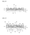
- FIGS. 1A to 1Z and 2A to 2C are cross-sectional views of a wiring substrate in the course of manufacturing thereof according to a first embodiment
- FIGS. 3A and 3B are overall plan views of a laminated sheet in the course of manufacturing the wiring substrate according to the first embodiment
- FIG. 4 is an overall plan view of an inorganic dielectric layer in the course of manufacturing the wiring substrate according to the first embodiment
- FIG. 5 is a cross-sectional view illustrating an example of method of using the wiring substrate according to the first embodiment
- FIG. 6 is a cross-sectional view illustrating another example of method of using the wiring substrate according to the first embodiment
- FIG. 7 is a cross-sectional view of a wiring substrate according to a second embodiment.
- FIG. 8 is a cross-sectional view of a wiring substrate according to a third embodiment.
- FIGS. 1A to 1Z and 2A to 2C are cross-sectional views of a wiring substrate in the course of manufacturing thereof according to a first embodiment.
- a laminated sheet 1 is fabricated in which an inorganic dielectric layer 3 is sandwiched between a first conductor layer 2 and a second conductor layer 4 .
- the second conductor layer 4 of the laminated sheet 1 is a metal foil, and a nickel foil having a thickness of approximately 0.28 ⁇ m is formed as the second conductor layer 4 in this example.
- a surface 4 x of the second conductor layer 4 is mirror polished and has a surface roughness smaller than 0.1 ⁇ m, which is favorable flatness than a plating film having a surface roughness larger than 0.3 ⁇ m.
- the inorganic dielectric layer 3 is a barium titanate (BaTiO 3 ) layer which is formed on the second conductor layer 4 by a sputtering method.
- the first conductor layer 2 is a copper layer having a thickness of approximately 18 ⁇ m which is formed on the inorganic dielectric layer 3 by the sputtering method.
- the thickness of the inorganic dielectric layer 3 is thinned to approximately 0.9 ⁇ m in this example.
- the inorganic dielectric layer 3 functions as a capacitor dielectric layer of the wiring substrate as described later, and the material thereof is not limited to the abovementioned barium titanate.
- any of Strontium titanate (SrTiO 3 ), lead zirconate titanate (PZT), and lead lanthanum zirconate titanate (PLZT) may be used as the material of the inorganic dielectric layer 3 .
- any of lead niobium zirconate titanate (PNZT), lead calcium zirconate titanate (PCZT), lead strontium zirconate titanate (PSZT), and tantalum oxide (TaO 3 , Ta 2 O 5 ) may be used as the material of the inorganic dielectric layer 3 .
- the laminated sheet 1 having a structure in which the conductor layers 2 and 4 sandwich therebetween the thin inorganic dielectric layer 3 formed by the sputtering method in this manner is also called as a thin film capacitor (TFC).
- TFC thin film capacitor
- the first conductor layer 2 is patterned to form a first conductor pattern 2 a .
- This patterning is performed by etching the first conductor layer 2 in wet etching which uses a copper chloride aqueous solution as an etchant, while using an unillustrated resist as a mask, and the resist is removed after the etching is completed.
- a core base member 11 is prepare, independent of the abovementioned laminated sheet 1 .
- the core base member 11 is, for example, a resin base member having a thickness of 0.3 mm to 9.4 mm in which glass fiber is impregnated with an epoxy resin.
- an epoxy resin layer is provided as an uncured first resin layer 12 to have a thickness of 5 ⁇ m to 100 ⁇ m.
- a copper foil having a thickness of approximately 18 ⁇ m is disposed over the first resin layer 12 as a first metal foil 13 .
- a copper foil having a thickness of approximately 35 ⁇ m is disposed over the first metal foil 13 as a second metal foil 14 .
- the second metal foil 14 has a planer size larger than that of the first metal foil 13 , and extends off from the first metal foil 13 by approximately 1 cm.
- the first resin layer 12 is heated at the temperature of approximately 180° C. and thus thermally cured.
- the second metal foil 14 has a planer size larger than that of the first metal foil 13 as described above, so that edge portions 14 a of the second metal foil 14 are bonded to the first resin layer 12 .
- the portion of the second metal foil 14 nearer to the center thereof than the edge portion 14 a is in a state where the air is excluded between the second metal foil 14 and the first metal foil 13 , and is brought into close contact with the first metal foil 13 due to atmospheric pressure.
- a first support substrate 15 including the first metal foil 13 and the second metal foil 14 bonded to the core base member 11 in this order is obtained.
- an uncured resin sheet having a thickness of approximately 5 ⁇ m to 100 ⁇ m is bonded to the second metal foil 14 , and the resin sheet is used as a second resin layer 16 .
- thermosetting epoxy resin with which a silica filler as an inorganic filler is kneaded is used as a material of the second resin layer 16 .
- the aforementioned laminated sheet 1 is again prepared, and the first conductor pattern 2 a of the laminated sheet 1 is faced with the second resin layer 16 .
- a frame 19 obtained by processing a copper foil having a thickness similar to that of the laminated sheet 1 is disposed around the laminated sheet 1 .
- the laminated sheet 1 and the frame 19 are pressed against the second resin layer 16 by a flat surface of a jig 100 in a vacuum.
- the first conductor pattern 2 a is embedded into the softened second resin layer 16 , so that the first conductor pattern 2 a of the laminated sheet 1 is bonded to the second resin layer 16 .
- the second resin layer 16 is heated at the temperature of approximately 170° C. to 180° C. for approximately 40 minutes to 80 minutes, thereby thermally curing the second resin layer 16 .
- the first support substrate 15 is thicker and harder than the laminated sheet 1 , flatness of the laminated sheet 1 becomes favorable by bonding the laminated sheet 1 to the first support substrate 15 in this manner.
- a copper layer is formed by an electrolytic plating method so as to have a thickness of from approximately 5 ⁇ m to 35 ⁇ m on the second conductor layer 4 , and the copper layer is used as a third conductor layer 17 .
- the second conductor layer 4 and the third conductor layer 17 are respectively patterned, and the patterned second conductor layer 4 is used as a second conductor pattern 4 a.
- This patterning is performed by wet etching the conductor layers 4 and 17 while using an unillustrated dry film resist as a mask, and the dry film resist is removed after the wet etching is completed.
- an etchant which can be used in this wet etching includes a copper chloride aqueous solution.
- the inorganic dielectric layer 3 does not dissolve in this etchant, so that the inorganic dielectric layer 3 is not patterned even when this step is performed.
- the respective conductor patterns 2 a and 4 a function as electrodes, and the inorganic dielectric layer 3 functions as a capacitor dielectric layer. Since the inorganic dielectric layer 3 is formed so as to have a thin thickness of approximately 0.9 ⁇ m by the sputtering method, the electrostatic capacitance of the capacitor Q can be increased.
- FIG. 3A is an overall plan view of the laminated sheet 1 after this step is completed seen from the first conductor pattern 2 a.
- the first conductor pattern 2 a is divided into a plurality of regions A to D in this example. Note that no first conductor pattern 2 a is present in a boundary portion between adjacent two regions among these regions A to D, and the respective first conductor patterns 2 a in the regions A to D are electrically separated from one another.
- the first conductor pattern 2 a is electrically connected to a power supply terminal of a semiconductor element and a motherboard. Therefore, by diving the first conductor pattern 2 a into the plurality of regions A to D in this manner, power supply voltages of different voltages can be applied to each region A to D, making it possible to use the semiconductor element and the motherboard which are driven by multiple kind of power supply voltages.
- FIG. 3B is an overall plan view of the laminated sheet 1 after this step is completed seen from the second conductor pattern 4 a.
- the second conductor pattern 4 a is not divided into a plurality of regions.
- the second conductor pattern 4 a is electrically connected to a ground terminal of the semiconductor element and the motherboard. Therefore, the second conductor pattern 4 a does not need to be divided for each power supply as in the first conductor pattern 2 a , and the second conductor pattern 4 a can be common to all the power supplies without being divided as is in this example.
- the material of the second conductor pattern 4 a is nickel, whose Young's modulus is higher than that of copper that is the material of the first conductor pattern 2 a . Therefore, by not dividing the second conductor pattern 4 a in this manner, the laminated sheet 1 becomes difficult to be deformed by a stress, which results in the favorable flatness of the substrate after being completely manufactured.
- an epoxy resin sheet is bonded to the second conductor pattern 4 a , and the resin sheet is thermally cured to form a first insulating layer 20 .
- the third conductor layer 17 whose material is copper, functions not only to reduce the resistance of the second conductor pattern 4 a , but also to increase the adhesion between the first insulating layer 20 and the second conductor pattern 4 a.
- the third conductor layer 17 may be omitted.
- first via holes 20 a and a second via hole 20 b are formed by laser beam in the first insulating layer 20 .
- the first via hole 20 a is formed in a first region I which locates on the first conductor pattern 2 a and where no second conductor pattern 4 a is present, and the inorganic dielectric layer 3 exposes in a bottom of the first via hole 20 a.
- the second via hole 20 b is formed in a second region II where the second conductor pattern 4 a is present, and the third conductor layer 17 exposes in a bottom of the second via hole 20 b.
- the inorganic dielectric layer 3 and the second conductor pattern 4 a are prevented from being opened by the laser.
- the inorganic dielectric layer 3 under the first via hole 20 a is removed by wet etching using a hydrochloric acid as an etchant.
- a hydrochloric acid as an etchant.
- the inorganic dielectric layer 3 under the first via hole 20 a is also removed by the laser simultaneously when the first via hole 20 a is formed by the laser.
- the power of the laser needs to be increased for processing the inorganic dielectric layer 3 formed of the inorganic material by the laser, so that there is a possibility that the first via hole 20 a is deformed due to the high-power laser.
- the inorganic dielectric layer 3 is preferably opened by wet etching as in the present embodiment.
- FIG. 4 is an overall plan view of the inorganic dielectric layer 3 of the laminated sheet 1 after this step is completed.
- the inorganic dielectric layer 3 is formed on the entire surface of the laminated sheet 1 except the first via holes 20 a.
- an electroless copper plating film 25 is formed so as to have a thickness of approximately 0.1 ⁇ m to 3 ⁇ m on the first insulating layer 20 and inner surfaces of the respective via holes 20 a and 20 b.
- an unillustrated dry resist film is bonded to the electroless copper plating film 25 ( FIG. 1L ).
- an electrolytic copper plating film is grown on a portion of the electroless copper plating film 25 which is not covered with the dry film resist, and thus the respective via holes 20 a and 20 b are filled with the electrolytic copper plating film.
- first and second via conductors 26 a and 26 b are formed in the first and second via holes 20 a and 20 b respectively, and a first wiring layer 26 x is formed on the first insulating layer 20 .
- Such a method of forming the wiring and the via conductors is called a semi-additive method.
- the second via conductor 26 b is electrically connected to the second conductor pattern 4 a
- the first via conductor 26 a skips the second conductor pattern 4 a
- the via conductor which skips one layer and is connected to the next layer in this manner is called a skip via in some cases.
- the both electrodes of the capacitor Q can easily be drawn out to the surface of the first insulating layer 20 .
- the second via conductor 26 b is electrically connected to the second conductor pattern 4 a via the third conductor layer 17 , the second via conductor 26 b is directly connected to the second conductor pattern 4 a in the case where the third conductor layer 17 is omitted.
- a first multilayer wiring layer 31 is formed on the respective via conductors 26 a and 26 b.
- the number of wiring layers in the first multilayer wiring layer 31 is not particularly limited, the number of wiring layers in this example is five layers.
- a first solder resist layer 32 is formed on a topmost layer of the first multilayer wiring layer 31 by a printing method. Note that a part of the topmost first wiring layer 26 x is not covered with the first solder resist layer 32 but is exposed.
- edge portions of the first support substrate 15 on which the first multilayer wiring layer 31 is formed in the manner described above are cut out along first cut-out lines C 1 .
- the first cut-out line C 1 is set so as to pass through an inner side than the portion where the second metal foil 14 is bonded to the first resin layer 12 in the edge portion of the first support substrate 15 .
- the second metal foil 14 after the cutting is in a state of contacting with the first metal foil 13 by atmospheric pressure, and can be easily peeled off from the first metal foil 13 by an external force.
- the second metal foil 14 is peeled off from the first metal foil 13 .
- the laminated sheet 1 and the first multilayer wiring layer 31 are peeled off from the first support substrate 15 .
- the second metal foil 14 constituting the first support substrate 15 is moved to the laminated sheet 1 by the adhesive strength of the second resin layer 16 .
- the second metal foil 14 moved to the laminated sheet 1 is removed by wet etching while using a copper chloride aqueous solution as an etchant for example, and a surface 16 a of the second resin layer 16 is caused to expose.
- a second support substrate 38 in which a copper foil 36 and a third resin layer 37 are formed in this order on a core base member 35 is prepared.
- the core base member 35 is a resin base member having a thickness of 0.3 mm to 9.4 mm in which glass fiber is impregnated with an epoxy resin, for example, and is thicker than the aforementioned first multilayer wiring layer 31 .
- the third resin layer 37 is an uncured epoxy resin layer having a thickness of 5 ⁇ m to 100 ⁇ m, for example.
- a copper foil having a thickness of approximately 5 ⁇ m to 35 ⁇ m and serving as a metal foil 39 is disposed over the second support substrate 38 , and the first multilayer wiring layer 31 is disposed over the metal foil 39 .
- the metal foil 39 has a planer size smaller than that of the first multilayer wiring layer 31 and, in this example, end portions of the metal foil 39 are positioned inward of outer circumference side surfaces of the first multilayer wiring layer 31 by approximately 1 cm.
- the third resin layer 37 is softened at the temperature of approximately 100° C. in a vacuum, the first multilayer wiring layer 31 and the metal foil 39 are pressed against the third resin layer 37 to bond the metal foil 39 to the third resin layer 37 .
- the metal foil 39 has a planer size smaller than that of the first multilayer wiring layer 31 in this example, the first solder resist layer 32 is bonded to the third resin layer 37 in edge portions of the second support substrate 38 .
- the air between the first multilayer wiring layer 31 and the metal foil 39 is excluded in a portion of the second support substrate 38 nearer to the center thereof, so that the first multilayer wiring layer 31 is brought into close contact with the metal foil 39 due to atmospheric pressure.
- the flatness of the first multilayer wiring layer 31 becomes favorable by bonding the first multilayer wiring layer 31 to the second support substrate 38 in this manner, since the second support substrate 38 is thicker and harder than the first multilayer wiring layer 31 .
- a resin sheet of a thermosetting epoxy resin is bonded onto the second resin layer 16 as a covering layer 43 , and the second resin layer 16 and the covering layer 43 constitute a second insulating layer 44 .
- the covering layer 43 includes not only the epoxy resin but also a silica filler as an inorganic filler. Moreover, the thickness of the covering layer 43 is 10 ⁇ m, for example.
- the covering layer 43 is heated at the temperature of approximately 170° C. for approximately one hour to partially cure the covering layer 43 .
- the process in which the resin is not entirely cured but is partially cured is also called preliminary curing.
- a surface layer portion of the covering layer 43 is etched with a strong alkaline solution to cause a silica filler contained in the surface layer portion to elute into the strong alkaline solution.
- unevenness associated with the silica filler is formed in a surface 43 x of the covering layer 43 .
- Such a process is called desmear process.
- the desmear process is performed on the second resin layer 16 under the covering layer 43 .
- the second resin layer 16 is completely thermally cured in the step of FIG. 1G already, it is difficult to dissolve the second resin layer 16 with the strong alkaline solution, and hence it is difficult to form unevenness on the surface of the second resin layer 16 . Therefore, as in the present embodiment, it is preferable to form the covering layer 43 on the second resin layer 16 , and perform the desmear process on the covering layer 43 which is not completely thermally cured.
- the covering layer 43 is heated at the temperature of approximately 180° C. for approximately one hour to completely thermally cure the covering layer 43 .
- a third via hole 44 a and fourth via holes 44 b are formed in the second insulating layer 44 by laser beam.
- the third via hole 44 a is formed in a third region III which locates on the second conductor pattern 4 a and where no first conductor pattern 2 a is present, and the inorganic dielectric layer 3 exposes in a bottom of the third via hole 44 a.
- the fourth via hole 44 b is formed in a fourth region IV where the first conductor pattern 2 a is present, and the first conductor pattern 2 a exposes in a bottom of the fourth via hole 44 b.
- the inorganic dielectric layer 3 and the first conductor pattern 2 a are prevented from being opened by adjusting the power of the laser.
- the inorganic dielectric layer 3 under the third via hole 44 a is removed by wet etching while using a hydrochloric acid as an etchant, and the second conductor pattern 4 a is caused to expose in the bottom of the third via hole 44 a.
- the shape of the third via hole 44 a is prevented from being deformed which would occur when the inorganic dielectric layer 3 is opened by laser.
- third and fourth via conductors 46 a and 46 b are formed in the third and fourth via holes 44 a and 44 b respectively, and a second wiring layer 46 x is formed on the second insulating layer 44 .
- the respective via conductors 46 a and 46 b and the second wiring layer 46 x are formed of an electroless copper plating film and an electrolytic copper plating film formed thereon.
- the third via conductor 46 a has the skip via structure, in which the third via conductor 46 a skips the first conductor pattern 2 a and is connected to the second conductor pattern 4 a under the first conductor pattern 2 a.
- This skip via structure can easily draw out both electrodes of the capacitor Q to the surface of the second insulating layer 44 with the same reason as the step of FIG. 1M .
- the conductor patterns 2 a and 4 a are not opened by laser in the present embodiment. Therefore, the first conductor pattern 2 a is interposed between the first via conductor 26 a and the fourth via conductor 46 b , and the second conductor pattern 4 a is interposed between the second via conductor 26 b and the third via conductor 46 a.
- the adhesion between the second wiring layer 46 x and the covering layer 43 can be increased.
- a second solder resist layer 47 is formed on the second insulating layer 44 by the printing method. Note that a part of the second wiring layer 46 x is not covered with the second solder resist layer 47 but is exposed.
- a gold layer 49 is formed so as to have a thickness of approximately 0.001 ⁇ m to 0.5 ⁇ m on a surface of the part of the second wiring layer 46 x which is not covered with the second solder resist layer 47 by the plating method.
- portions from the second support substrate 38 to the topmost second solder resist layer 47 are cut out along second cut-out lines C 2 .
- the second cut-out line C 2 is set so as to pass through an inner side than a portion where the first solder resist layer 32 is bonded to the third resin layer 37 in an edge portion of the second support substrate 38 . Therefore, the first multilayer wiring layer 31 after the cutting is only in contact with the metal foil 39 by atmospheric pressure, and can be easily peeled off from the metal foil 39 by an external force.
- the shape and the size after the cutting are not specially limited.
- the portions from the second support substrate 38 to the second solder resist layer 47 are cut out into the square shape whose one length is 35 mm in planer view.
- the first multilayer wiring layer 31 and the laminated sheet 1 thereon are peeled off from the metal foil 39 .
- a soldering paste as a presolder 50 is applied onto the second wiring layer 46 x whose wettability is improved with the gold layer 49 . Further, after the presolder 50 is subjected to reflow to be made into a spherical shape, an upper portion of the presolder 50 is made flat by coining. Note that in order to perform the coining, the presolder 50 may be crushed flat by an unillustrated jig, for example.
- This wiring substrate 52 is a coreless multilayer wiring substrate including no core substrate, and can be made thinner by the thickness of the core substrate.
- the electrostatic capacitance of the capacitor Q embedded in the wiring substrate 52 can be increased by forming the inorganic dielectric layer 3 to be thin by the sputtering method.
- the second conductor pattern 4 a can be easily formed even in the laminated sheet 1 provided with the thin inorganic dielectric layer 3 having a thickness of 2 ⁇ m or less, by patterning the second conductor layer 4 in the step of FIG. 1I .
- the first multilayer wiring layer 31 can be formed on the laminated sheet 1 by the build-up method, without using the dedicated process or facility to the thin laminated sheet 1 .
- the first via conductor 26 a having a skip via structure is connected to the first conductor pattern 2 a . Therefore, the first conductor pattern 2 a can be electrically drawn out to the same side as the first via conductor 26 a.
- the method of using the wiring substrate 52 is not particularly limited.
- FIG. 5 is a cross-sectional view illustrating an example of method of using the wiring substrate 52 .
- a semiconductor element 60 is provided at the first conductor pattern 2 a side of the capacitor Q, and a circuit substrate 70 is provided at the second conductor pattern 4 a side of the capacitor Q.
- the semiconductor element 60 includes a first power supply terminal 60 a and a first ground terminal 60 b , and first soldering bumps 61 are jointed onto these terminals. Further, in the state where the first soldering bumps 61 are mounted on the presolder 50 (see FIG. 2C ), the first soldering bumps 61 are heated to be ref lowed.
- the fourth via conductor 46 b is electrically connected to the first power supply terminal 60 a
- the third via conductor 46 a is electrically connected to the first ground terminal 60 b.
- the circuit substrate 70 includes a second power supply terminal 70 a and a second ground terminal 70 b .
- second soldering bumps 71 are disposed between the lowermost wiring layer 26 x of the wiring substrate 52 and the respective terminals 70 a and 70 b , and the second soldering bumps 71 are heated to be reflowed.
- the second power supply terminal 70 a is electrically connected to the first via conductor 26 a
- the second ground terminal 70 b is electrically connected to the second via conductor 26 b.
- one of the electrodes of the capacitor Q is electrically connected to each of the power supply terminals 60 a and 70 a
- the other electrode of the capacitor Q is electrically connected to each of the ground terminals 60 b and 70 b , so that the capacitor Q functions as a decoupling capacitor which reduces noise in the power supply terminals 60 a and 70 a.
- the present embodiment is not limited to the above.
- FIG. 6 is a cross-sectional view illustrating another method of using the wiring substrate 52 . Note that, in FIG. 6 , the same elements as those in in FIG. 5 are given with the same reference numerals as in FIG. 5 , and the description thereof will be omitted below.
- a plurality of the semiconductor elements 60 are mounted onto the wiring substrate 52 .
- the power supply voltage of each semiconductor element 60 is not particularly limited.
- the first conductor pattern 2 a is divided into the regions A to D (see FIG. 3A ) of different power supply voltages. Therefore, by allocating one semiconductor element 60 to each of the regions A to D, the respective semiconductor elements 60 can be driven at the different power supply voltages.
- FIG. 7 is a cross-sectional view of a wiring substrate according to the present embodiment.
- a second multilayer wiring layer 53 is formed on the respective via conductors 46 a and 46 b.
- the first multilayer wiring layer 31 and the second multilayer wiring layer 53 are respectively formed on both surfaces of the capacitor Q, so that the density of the wirings in the wiring substrate 52 can be increased.
- the number of layers in each of the first multilayer wiring layer 31 and the second multilayer wiring layer 53 is not particularly limited.
- the capacitor Q it is preferable to make the capacitor Q to be closer to the semiconductor element 60 , by employing such a structure where the number of the second wiring layers 46 x in the second multilayer wiring layer 53 is smaller than the number of the second wiring layers 26 x in the first multilayer wiring layer 31 .
- This structure shortens a wiring length from the capacitor Q to the semiconductor element 60 , so that a signal delay due to the wiring length is suppressed, and an effect of the decoupling by the capacitor Q can be increased.
- FIG. 8 is a cross-sectional view of a wiring substrate according to the present embodiment.
- FIG. 8 the same elements as those in in the first and second embodiments are given with the same reference numerals as in these embodiments, and the description thereof will be omitted below.
- a glass cloth-containing epoxy resin is used as a material of one insulating layer 20 z among the plurality of the first insulating layers 20 . This results in the higher Young's modulus of the first insulating layer 20 z than that of the other first insulating layers 20 with no glass cloth.
- the number of the first insulating layers 20 which are laminated under the first insulating layer 20 z is one, which is the same as the number of the second insulating layers 44 which are laminated on the laminated sheet 1 .
- the second conductor pattern 4 a of the laminated sheet 1 also uses nickel having a high Young's modulus as a material. Therefore, in the present embodiment, the laminated sheet 1 and the first insulating layer 20 z both having a high Young's modulus are disposed so as to be approximately linearly symmetrical with each other with respect to a center line P of the substrate. This structure can reinforce the wiring substrate 55 from the upper and lower sides in good balance by the laminated sheet 1 and the second insulating layer 20 z , and effectively suppress warpage of the wiring substrate 55 .
- the inorganic dielectric layer 3 of the laminated sheet 1 is used as a capacitor dielectric layer in the above, the intended use of the inorganic dielectric layer 3 is not limited to this.
- the inorganic dielectric layer 3 may be used as the first insulating layer 20 constituting the first multilayer wiring layer 31 or the second insulating layer 44 constituting the second multilayer wiring layer 53 , thereby obtaining the thin wiring substrate 52 .
- the aforementioned wiring substrate 52 is a coreless substrate
- the present embodiments may be applied to a wiring substrate provided with a core base member to form the thin inorganic dielectric layer 3 on the wiring substrate.
Landscapes
- Engineering & Computer Science (AREA)
- Microelectronics & Electronic Packaging (AREA)
- Manufacturing & Machinery (AREA)
- Chemical & Material Sciences (AREA)
- Chemical Kinetics & Catalysis (AREA)
- General Chemical & Material Sciences (AREA)
- Physics & Mathematics (AREA)
- Optics & Photonics (AREA)
- Production Of Multi-Layered Print Wiring Board (AREA)
- Parts Printed On Printed Circuit Boards (AREA)
- Geometry (AREA)
Abstract
Description
Claims (10)
Applications Claiming Priority (2)
| Application Number | Priority Date | Filing Date | Title |
|---|---|---|---|
| JP2015-199256 | 2015-10-07 | ||
| JP2015199256A JP6628544B2 (en) | 2015-10-07 | 2015-10-07 | Manufacturing method of wiring board |
Publications (2)
| Publication Number | Publication Date |
|---|---|
| US20170103944A1 US20170103944A1 (en) | 2017-04-13 |
| US10109571B2 true US10109571B2 (en) | 2018-10-23 |
Family
ID=58498904
Family Applications (1)
| Application Number | Title | Priority Date | Filing Date |
|---|---|---|---|
| US15/278,798 Active US10109571B2 (en) | 2015-10-07 | 2016-09-28 | Wiring substrate and manufacturing method of wiring substrate |
Country Status (2)
| Country | Link |
|---|---|
| US (1) | US10109571B2 (en) |
| JP (1) | JP6628544B2 (en) |
Cited By (1)
| Publication number | Priority date | Publication date | Assignee | Title |
|---|---|---|---|---|
| US20230036907A1 (en) * | 2020-05-07 | 2023-02-02 | Murata Manufacturing Co., Ltd. | Multilayer substrate module |
Families Citing this family (8)
| Publication number | Priority date | Publication date | Assignee | Title |
|---|---|---|---|---|
| US10026687B1 (en) * | 2017-02-20 | 2018-07-17 | Globalfoundries Inc. | Metal interconnects for super (skip) via integration |
| US9805972B1 (en) * | 2017-02-20 | 2017-10-31 | Globalfoundries Inc. | Skip via structures |
| JP6826947B2 (en) * | 2017-05-18 | 2021-02-10 | 新光電気工業株式会社 | Wiring board, manufacturing method of wiring board |
| US10485111B2 (en) * | 2017-07-12 | 2019-11-19 | Globalfoundries Inc. | Via and skip via structures |
| US11596056B2 (en) * | 2018-10-02 | 2023-02-28 | Skyworks Solutions, Inc. | Methods and devices related to reduced packaging substrate deformation |
| KR20220086924A (en) | 2020-12-17 | 2022-06-24 | 삼성전기주식회사 | Printed circuit board |
| KR102932521B1 (en) * | 2021-03-09 | 2026-03-04 | 삼성전자주식회사 | Semiconductor package |
| TWI800129B (en) * | 2021-12-01 | 2023-04-21 | 財團法人工業技術研究院 | Conductive circuit carrier module |
Citations (9)
| Publication number | Priority date | Publication date | Assignee | Title |
|---|---|---|---|---|
| US20020060091A1 (en) * | 2000-09-22 | 2002-05-23 | Kabushiki Kaisha Toshiba | Ceramic circuit board and method of manufacturing the same |
| US20030086248A1 (en) * | 2000-05-12 | 2003-05-08 | Naohiro Mashino | Interposer for semiconductor, method for manufacturing same, and semiconductor device using same |
| JP2004140254A (en) | 2002-10-18 | 2004-05-13 | Toray Ind Inc | Multilayer circuit board member and method of manufacturing multilayer circuit board |
| JP2004235323A (en) | 2003-01-29 | 2004-08-19 | Fujitsu Ltd | Manufacturing method of wiring board |
| JP2005044833A (en) | 2003-07-22 | 2005-02-17 | Furukawa Electric Co Ltd:The | Electronic component built-in substrate, semiconductor package, and electronic component built-in substrate manufacturing method |
| WO2006016589A1 (en) | 2004-08-11 | 2006-02-16 | Mitsui Mining & Smelting Co., Ltd. | Method for producing dielectric layer-constituting material, dielectric layer-constituting material produced by such method, method for manufacturing capacitor circuit-forming member using such dielectric layer-constituting material, capacitor circuit-forming member obtained by such method, and multilayer printed wiring boa |
| US20060131069A1 (en) | 2004-12-20 | 2006-06-22 | Noriyoshi Shimizu | Method of manufacturing wiring substrate to which semiconductor chip is mounted |
| US20070069363A1 (en) | 2005-09-28 | 2007-03-29 | Tdk Corporation | Semiconductor IC-embedded substrate and method for manufacturing same |
| US20070105278A1 (en) | 2004-06-25 | 2007-05-10 | Ibiden Co., Ltd | Printed wiring board and method of manufacturing the same |
Family Cites Families (3)
| Publication number | Priority date | Publication date | Assignee | Title |
|---|---|---|---|---|
| JP3976954B2 (en) * | 1999-08-27 | 2007-09-19 | 新光電気工業株式会社 | Multilayer wiring board manufacturing method and semiconductor device |
| KR100923895B1 (en) * | 2005-06-13 | 2009-10-28 | 이비덴 가부시키가이샤 | Printed wiring board |
| US8115113B2 (en) * | 2007-11-30 | 2012-02-14 | Ibiden Co., Ltd. | Multilayer printed wiring board with a built-in capacitor |
-
2015
- 2015-10-07 JP JP2015199256A patent/JP6628544B2/en active Active
-
2016
- 2016-09-28 US US15/278,798 patent/US10109571B2/en active Active
Patent Citations (17)
| Publication number | Priority date | Publication date | Assignee | Title |
|---|---|---|---|---|
| US20030086248A1 (en) * | 2000-05-12 | 2003-05-08 | Naohiro Mashino | Interposer for semiconductor, method for manufacturing same, and semiconductor device using same |
| US20020060091A1 (en) * | 2000-09-22 | 2002-05-23 | Kabushiki Kaisha Toshiba | Ceramic circuit board and method of manufacturing the same |
| JP2004140254A (en) | 2002-10-18 | 2004-05-13 | Toray Ind Inc | Multilayer circuit board member and method of manufacturing multilayer circuit board |
| JP2004235323A (en) | 2003-01-29 | 2004-08-19 | Fujitsu Ltd | Manufacturing method of wiring board |
| US20040211751A1 (en) | 2003-01-29 | 2004-10-28 | Takashi Shuto | Method of manufacturing circuit board |
| JP2005044833A (en) | 2003-07-22 | 2005-02-17 | Furukawa Electric Co Ltd:The | Electronic component built-in substrate, semiconductor package, and electronic component built-in substrate manufacturing method |
| US20080104833A1 (en) | 2004-06-25 | 2008-05-08 | Ibiden Co., Ltd | Printed wiring board and method of manufacturing the same |
| US20070105278A1 (en) | 2004-06-25 | 2007-05-10 | Ibiden Co., Ltd | Printed wiring board and method of manufacturing the same |
| US20100193227A1 (en) | 2004-06-25 | 2010-08-05 | Ibiden Co., Ltd | Printed wiring board and method of manufacturing the same |
| JP2012033968A (en) | 2004-06-25 | 2012-02-16 | Ibiden Co Ltd | Printed wiring board and method of manufacturing the same |
| WO2006016589A1 (en) | 2004-08-11 | 2006-02-16 | Mitsui Mining & Smelting Co., Ltd. | Method for producing dielectric layer-constituting material, dielectric layer-constituting material produced by such method, method for manufacturing capacitor circuit-forming member using such dielectric layer-constituting material, capacitor circuit-forming member obtained by such method, and multilayer printed wiring boa |
| US20080289865A1 (en) | 2004-08-11 | 2008-11-27 | Mitsui Mining & Smelting Co., Ltd. | Method for Manufacturing Dielectric Layer Constituting Material, Dielectric Layer Constituting Material Obtained Thereby; Method for Manufacturing Capacitor Circuit Forming Piece Using Dielectric Layer Constituting Material, Capacitor Circuit Forming Piece Obtained Thereby; and Multi-Layer Printed Wiring Board Obtained by Using Dielectric Layer Constituting Material and/or Capacitor Circuit Forming Piece |
| US20060131069A1 (en) | 2004-12-20 | 2006-06-22 | Noriyoshi Shimizu | Method of manufacturing wiring substrate to which semiconductor chip is mounted |
| JP2006173544A (en) | 2004-12-20 | 2006-06-29 | Shinko Electric Ind Co Ltd | Wiring board manufacturing method |
| US20070069363A1 (en) | 2005-09-28 | 2007-03-29 | Tdk Corporation | Semiconductor IC-embedded substrate and method for manufacturing same |
| JP2007123797A (en) | 2005-09-28 | 2007-05-17 | Tdk Corp | Semiconductor IC-embedded substrate and manufacturing method thereof |
| US20090218678A1 (en) | 2005-09-28 | 2009-09-03 | Tdk Corporation | Semiconductor ic-embedded substrate and method for manufacturing same |
Cited By (2)
| Publication number | Priority date | Publication date | Assignee | Title |
|---|---|---|---|---|
| US20230036907A1 (en) * | 2020-05-07 | 2023-02-02 | Murata Manufacturing Co., Ltd. | Multilayer substrate module |
| US12273994B2 (en) * | 2020-05-07 | 2025-04-08 | Murata Manufacturing Co., Ltd. | Multilayer substrate module with filter function |
Also Published As
| Publication number | Publication date |
|---|---|
| JP2017073458A (en) | 2017-04-13 |
| JP6628544B2 (en) | 2020-01-08 |
| US20170103944A1 (en) | 2017-04-13 |
Similar Documents
| Publication | Publication Date | Title |
|---|---|---|
| US10109571B2 (en) | Wiring substrate and manufacturing method of wiring substrate | |
| US11375620B2 (en) | Multi-layer ceramic electronic component, method of producing a multi-layer ceramic electronic component, and substrate with a built-in electronic component | |
| US8116066B2 (en) | Method of manufacturing electronic component built-in substrate | |
| US9947466B2 (en) | Electronic component | |
| KR102032171B1 (en) | Electronic component built-in substrate and method of manufacturing the same | |
| JP5111342B2 (en) | Wiring board | |
| US9504169B2 (en) | Printed circuit board having embedded electronic device and method of manufacturing the same | |
| US10306770B2 (en) | Thin-film capacitor manufacturing method, integrated circuit mounting substrate, and semiconductor device equipped with the substrate | |
| JP2011258772A (en) | Wiring board and manufacturing method thereof, and semiconductor device | |
| JP2009267310A (en) | Capacitor component, its manufacturing method and semiconductor package | |
| US20160255717A1 (en) | Multilayer wiring board | |
| WO2018128095A1 (en) | Circuit board, method for manufacturing circuit board, and electronic device | |
| US9750134B2 (en) | Method for producing a printed circuit board with multilayer sub-areas in sections | |
| JP5286072B2 (en) | Wiring board and manufacturing method thereof | |
| JP4351148B2 (en) | Wiring board manufacturing method | |
| JP2006186238A6 (en) | Wiring board manufacturing method | |
| JP2008112790A (en) | Semiconductor package and manufacturing method thereof | |
| US9433108B2 (en) | Method of fabricating a circuit board structure having an embedded electronic element | |
| CN102737842A (en) | Thin film capacitor, mounting substrate, and method of manufacturing the mounting substrate | |
| WO2017183135A1 (en) | Circuit board, method for manufacturing circuit board, and electronic device | |
| JP4731394B2 (en) | Electronic component built-in substrate and manufacturing method thereof | |
| KR101969643B1 (en) | Rigid flexible circuit board manufacturing method | |
| JP5283492B2 (en) | Wiring board | |
| US20160247753A1 (en) | Cavity substrate and method of manufacturing the same | |
| JP2010141029A (en) | Printed wiring board and method of manufacturing the same |
Legal Events
| Date | Code | Title | Description |
|---|---|---|---|
| AS | Assignment |
Owner name: FUJITSU LIMITED, JAPAN Free format text: ASSIGNMENT OF ASSIGNORS INTEREST;ASSIGNORS:FUKUI, KEI;ARAI, KAZUYA;KOMEMURA, KOJI;AND OTHERS;SIGNING DATES FROM 20160810 TO 20160916;REEL/FRAME:039925/0450 Owner name: SONY CORPORATION, JAPAN Free format text: ASSIGNMENT OF ASSIGNORS INTEREST;ASSIGNORS:FUKUI, KEI;ARAI, KAZUYA;KOMEMURA, KOJI;AND OTHERS;SIGNING DATES FROM 20160810 TO 20160916;REEL/FRAME:039925/0450 |
|
| STCF | Information on status: patent grant |
Free format text: PATENTED CASE |
|
| AS | Assignment |
Owner name: FUJITSU INTERCONNECT TECHNOLOGIES LIMITED, JAPAN Free format text: ASSIGNMENT OF ASSIGNORS INTEREST;ASSIGNOR:FUJITSU LIMITED;REEL/FRAME:052345/0895 Effective date: 20200327 |
|
| MAFP | Maintenance fee payment |
Free format text: PAYMENT OF MAINTENANCE FEE, 4TH YEAR, LARGE ENTITY (ORIGINAL EVENT CODE: M1551); ENTITY STATUS OF PATENT OWNER: LARGE ENTITY Year of fee payment: 4 |
|
| AS | Assignment |
Owner name: FICT LIMITED, JAPAN Free format text: CHANGE OF NAME;ASSIGNOR:FUJITSU INTERCONNECT TECHNOLOGIES LIMITED;REEL/FRAME:063881/0638 Effective date: 20220110 |
|
| MAFP | Maintenance fee payment |
Free format text: PAYMENT OF MAINTENANCE FEE, 8TH YEAR, LARGE ENTITY (ORIGINAL EVENT CODE: M1552); ENTITY STATUS OF PATENT OWNER: LARGE ENTITY Year of fee payment: 8 |