US10102822B2 - Array substrate, manufacturing method thereof, control method, control assembly, and display device - Google Patents
Array substrate, manufacturing method thereof, control method, control assembly, and display device Download PDFInfo
- Publication number
- US10102822B2 US10102822B2 US15/176,742 US201615176742A US10102822B2 US 10102822 B2 US10102822 B2 US 10102822B2 US 201615176742 A US201615176742 A US 201615176742A US 10102822 B2 US10102822 B2 US 10102822B2
- Authority
- US
- United States
- Prior art keywords
- thin film
- film transistor
- electrode
- array substrate
- photosensitive
- Prior art date
- Legal status (The legal status is an assumption and is not a legal conclusion. Google has not performed a legal analysis and makes no representation as to the accuracy of the status listed.)
- Active
Links
- 239000000758 substrate Substances 0.000 title claims abstract description 126
- 238000000034 method Methods 0.000 title claims abstract description 18
- 238000004519 manufacturing process Methods 0.000 title abstract description 15
- 239000010409 thin film Substances 0.000 claims abstract description 83
- 230000000694 effects Effects 0.000 claims description 12
- 238000005401 electroluminescence Methods 0.000 description 12
- 238000007796 conventional method Methods 0.000 description 6
- 238000010586 diagram Methods 0.000 description 3
- 238000000059 patterning Methods 0.000 description 3
- 239000010416 ion conductor Substances 0.000 description 2
- 239000000463 material Substances 0.000 description 2
- 229920000642 polymer Polymers 0.000 description 2
- 239000011347 resin Substances 0.000 description 2
- 229920005989 resin Polymers 0.000 description 2
- 230000007547 defect Effects 0.000 description 1
- 230000006870 function Effects 0.000 description 1
- 230000015654 memory Effects 0.000 description 1
- 230000000116 mitigating effect Effects 0.000 description 1
Images


Classifications
-
- G—PHYSICS
- G09—EDUCATION; CRYPTOGRAPHY; DISPLAY; ADVERTISING; SEALS
- G09G—ARRANGEMENTS OR CIRCUITS FOR CONTROL OF INDICATING DEVICES USING STATIC MEANS TO PRESENT VARIABLE INFORMATION
- G09G5/00—Control arrangements or circuits for visual indicators common to cathode-ray tube indicators and other visual indicators
- G09G5/10—Intensity circuits
-
- H—ELECTRICITY
- H01—ELECTRIC ELEMENTS
- H01L—SEMICONDUCTOR DEVICES NOT COVERED BY CLASS H10
- H01L27/00—Devices consisting of a plurality of semiconductor or other solid-state components formed in or on a common substrate
- H01L27/02—Devices consisting of a plurality of semiconductor or other solid-state components formed in or on a common substrate including semiconductor components specially adapted for rectifying, oscillating, amplifying or switching and having at least one potential-jump barrier or surface barrier; including integrated passive circuit elements with at least one potential-jump barrier or surface barrier
- H01L27/12—Devices consisting of a plurality of semiconductor or other solid-state components formed in or on a common substrate including semiconductor components specially adapted for rectifying, oscillating, amplifying or switching and having at least one potential-jump barrier or surface barrier; including integrated passive circuit elements with at least one potential-jump barrier or surface barrier the substrate being other than a semiconductor body, e.g. an insulating body
- H01L27/1214—Devices consisting of a plurality of semiconductor or other solid-state components formed in or on a common substrate including semiconductor components specially adapted for rectifying, oscillating, amplifying or switching and having at least one potential-jump barrier or surface barrier; including integrated passive circuit elements with at least one potential-jump barrier or surface barrier the substrate being other than a semiconductor body, e.g. an insulating body comprising a plurality of TFTs formed on a non-semiconducting substrate, e.g. driving circuits for AMLCDs
-
- H—ELECTRICITY
- H01—ELECTRIC ELEMENTS
- H01L—SEMICONDUCTOR DEVICES NOT COVERED BY CLASS H10
- H01L27/00—Devices consisting of a plurality of semiconductor or other solid-state components formed in or on a common substrate
- H01L27/02—Devices consisting of a plurality of semiconductor or other solid-state components formed in or on a common substrate including semiconductor components specially adapted for rectifying, oscillating, amplifying or switching and having at least one potential-jump barrier or surface barrier; including integrated passive circuit elements with at least one potential-jump barrier or surface barrier
- H01L27/12—Devices consisting of a plurality of semiconductor or other solid-state components formed in or on a common substrate including semiconductor components specially adapted for rectifying, oscillating, amplifying or switching and having at least one potential-jump barrier or surface barrier; including integrated passive circuit elements with at least one potential-jump barrier or surface barrier the substrate being other than a semiconductor body, e.g. an insulating body
- H01L27/1214—Devices consisting of a plurality of semiconductor or other solid-state components formed in or on a common substrate including semiconductor components specially adapted for rectifying, oscillating, amplifying or switching and having at least one potential-jump barrier or surface barrier; including integrated passive circuit elements with at least one potential-jump barrier or surface barrier the substrate being other than a semiconductor body, e.g. an insulating body comprising a plurality of TFTs formed on a non-semiconducting substrate, e.g. driving circuits for AMLCDs
- H01L27/124—Devices consisting of a plurality of semiconductor or other solid-state components formed in or on a common substrate including semiconductor components specially adapted for rectifying, oscillating, amplifying or switching and having at least one potential-jump barrier or surface barrier; including integrated passive circuit elements with at least one potential-jump barrier or surface barrier the substrate being other than a semiconductor body, e.g. an insulating body comprising a plurality of TFTs formed on a non-semiconducting substrate, e.g. driving circuits for AMLCDs with a particular composition, shape or layout of the wiring layers specially adapted to the circuit arrangement, e.g. scanning lines in LCD pixel circuits
-
- H—ELECTRICITY
- H01—ELECTRIC ELEMENTS
- H01L—SEMICONDUCTOR DEVICES NOT COVERED BY CLASS H10
- H01L27/00—Devices consisting of a plurality of semiconductor or other solid-state components formed in or on a common substrate
- H01L27/02—Devices consisting of a plurality of semiconductor or other solid-state components formed in or on a common substrate including semiconductor components specially adapted for rectifying, oscillating, amplifying or switching and having at least one potential-jump barrier or surface barrier; including integrated passive circuit elements with at least one potential-jump barrier or surface barrier
- H01L27/12—Devices consisting of a plurality of semiconductor or other solid-state components formed in or on a common substrate including semiconductor components specially adapted for rectifying, oscillating, amplifying or switching and having at least one potential-jump barrier or surface barrier; including integrated passive circuit elements with at least one potential-jump barrier or surface barrier the substrate being other than a semiconductor body, e.g. an insulating body
- H01L27/1214—Devices consisting of a plurality of semiconductor or other solid-state components formed in or on a common substrate including semiconductor components specially adapted for rectifying, oscillating, amplifying or switching and having at least one potential-jump barrier or surface barrier; including integrated passive circuit elements with at least one potential-jump barrier or surface barrier the substrate being other than a semiconductor body, e.g. an insulating body comprising a plurality of TFTs formed on a non-semiconducting substrate, e.g. driving circuits for AMLCDs
- H01L27/1259—Multistep manufacturing methods
-
- H—ELECTRICITY
- H01—ELECTRIC ELEMENTS
- H01L—SEMICONDUCTOR DEVICES NOT COVERED BY CLASS H10
- H01L27/00—Devices consisting of a plurality of semiconductor or other solid-state components formed in or on a common substrate
- H01L27/14—Devices consisting of a plurality of semiconductor or other solid-state components formed in or on a common substrate including semiconductor components sensitive to infrared radiation, light, electromagnetic radiation of shorter wavelength or corpuscular radiation and specially adapted either for the conversion of the energy of such radiation into electrical energy or for the control of electrical energy by such radiation
- H01L27/144—Devices controlled by radiation
- H01L27/1446—Devices controlled by radiation in a repetitive configuration
-
- H—ELECTRICITY
- H01—ELECTRIC ELEMENTS
- H01L—SEMICONDUCTOR DEVICES NOT COVERED BY CLASS H10
- H01L27/00—Devices consisting of a plurality of semiconductor or other solid-state components formed in or on a common substrate
- H01L27/15—Devices consisting of a plurality of semiconductor or other solid-state components formed in or on a common substrate including semiconductor components with at least one potential-jump barrier or surface barrier specially adapted for light emission
- H01L27/153—Devices consisting of a plurality of semiconductor or other solid-state components formed in or on a common substrate including semiconductor components with at least one potential-jump barrier or surface barrier specially adapted for light emission in a repetitive configuration, e.g. LED bars
- H01L27/156—Devices consisting of a plurality of semiconductor or other solid-state components formed in or on a common substrate including semiconductor components with at least one potential-jump barrier or surface barrier specially adapted for light emission in a repetitive configuration, e.g. LED bars two-dimensional arrays
-
- H—ELECTRICITY
- H01—ELECTRIC ELEMENTS
- H01L—SEMICONDUCTOR DEVICES NOT COVERED BY CLASS H10
- H01L31/00—Semiconductor devices sensitive to infrared radiation, light, electromagnetic radiation of shorter wavelength or corpuscular radiation and specially adapted either for the conversion of the energy of such radiation into electrical energy or for the control of electrical energy by such radiation; Processes or apparatus specially adapted for the manufacture or treatment thereof or of parts thereof; Details thereof
- H01L31/02—Details
- H01L31/0224—Electrodes
- H01L31/022408—Electrodes for devices characterised by at least one potential jump barrier or surface barrier
-
- H—ELECTRICITY
- H01—ELECTRIC ELEMENTS
- H01L—SEMICONDUCTOR DEVICES NOT COVERED BY CLASS H10
- H01L31/00—Semiconductor devices sensitive to infrared radiation, light, electromagnetic radiation of shorter wavelength or corpuscular radiation and specially adapted either for the conversion of the energy of such radiation into electrical energy or for the control of electrical energy by such radiation; Processes or apparatus specially adapted for the manufacture or treatment thereof or of parts thereof; Details thereof
- H01L31/08—Semiconductor devices sensitive to infrared radiation, light, electromagnetic radiation of shorter wavelength or corpuscular radiation and specially adapted either for the conversion of the energy of such radiation into electrical energy or for the control of electrical energy by such radiation; Processes or apparatus specially adapted for the manufacture or treatment thereof or of parts thereof; Details thereof in which radiation controls flow of current through the device, e.g. photoresistors
- H01L31/10—Semiconductor devices sensitive to infrared radiation, light, electromagnetic radiation of shorter wavelength or corpuscular radiation and specially adapted either for the conversion of the energy of such radiation into electrical energy or for the control of electrical energy by such radiation; Processes or apparatus specially adapted for the manufacture or treatment thereof or of parts thereof; Details thereof in which radiation controls flow of current through the device, e.g. photoresistors characterised by at least one potential-jump barrier or surface barrier, e.g. phototransistors
- H01L31/101—Devices sensitive to infrared, visible or ultraviolet radiation
- H01L31/112—Devices sensitive to infrared, visible or ultraviolet radiation characterised by field-effect operation, e.g. junction field-effect phototransistor
- H01L31/113—Devices sensitive to infrared, visible or ultraviolet radiation characterised by field-effect operation, e.g. junction field-effect phototransistor being of the conductor-insulator-semiconductor type, e.g. metal-insulator-semiconductor field-effect transistor
- H01L31/1136—Devices sensitive to infrared, visible or ultraviolet radiation characterised by field-effect operation, e.g. junction field-effect phototransistor being of the conductor-insulator-semiconductor type, e.g. metal-insulator-semiconductor field-effect transistor the device being a metal-insulator-semiconductor field-effect transistor
-
- H—ELECTRICITY
- H01—ELECTRIC ELEMENTS
- H01L—SEMICONDUCTOR DEVICES NOT COVERED BY CLASS H10
- H01L31/00—Semiconductor devices sensitive to infrared radiation, light, electromagnetic radiation of shorter wavelength or corpuscular radiation and specially adapted either for the conversion of the energy of such radiation into electrical energy or for the control of electrical energy by such radiation; Processes or apparatus specially adapted for the manufacture or treatment thereof or of parts thereof; Details thereof
- H01L31/12—Semiconductor devices sensitive to infrared radiation, light, electromagnetic radiation of shorter wavelength or corpuscular radiation and specially adapted either for the conversion of the energy of such radiation into electrical energy or for the control of electrical energy by such radiation; Processes or apparatus specially adapted for the manufacture or treatment thereof or of parts thereof; Details thereof structurally associated with, e.g. formed in or on a common substrate with, one or more electric light sources, e.g. electroluminescent light sources, and electrically or optically coupled thereto
- H01L31/14—Semiconductor devices sensitive to infrared radiation, light, electromagnetic radiation of shorter wavelength or corpuscular radiation and specially adapted either for the conversion of the energy of such radiation into electrical energy or for the control of electrical energy by such radiation; Processes or apparatus specially adapted for the manufacture or treatment thereof or of parts thereof; Details thereof structurally associated with, e.g. formed in or on a common substrate with, one or more electric light sources, e.g. electroluminescent light sources, and electrically or optically coupled thereto the light source or sources being controlled by the semiconductor device sensitive to radiation, e.g. image converters, image amplifiers or image storage devices
- H01L31/147—Semiconductor devices sensitive to infrared radiation, light, electromagnetic radiation of shorter wavelength or corpuscular radiation and specially adapted either for the conversion of the energy of such radiation into electrical energy or for the control of electrical energy by such radiation; Processes or apparatus specially adapted for the manufacture or treatment thereof or of parts thereof; Details thereof structurally associated with, e.g. formed in or on a common substrate with, one or more electric light sources, e.g. electroluminescent light sources, and electrically or optically coupled thereto the light source or sources being controlled by the semiconductor device sensitive to radiation, e.g. image converters, image amplifiers or image storage devices the light sources and the devices sensitive to radiation all being semiconductor devices characterised by at least one potential or surface barrier
- H01L31/153—Semiconductor devices sensitive to infrared radiation, light, electromagnetic radiation of shorter wavelength or corpuscular radiation and specially adapted either for the conversion of the energy of such radiation into electrical energy or for the control of electrical energy by such radiation; Processes or apparatus specially adapted for the manufacture or treatment thereof or of parts thereof; Details thereof structurally associated with, e.g. formed in or on a common substrate with, one or more electric light sources, e.g. electroluminescent light sources, and electrically or optically coupled thereto the light source or sources being controlled by the semiconductor device sensitive to radiation, e.g. image converters, image amplifiers or image storage devices the light sources and the devices sensitive to radiation all being semiconductor devices characterised by at least one potential or surface barrier formed in, or on, a common substrate
-
- H—ELECTRICITY
- H01—ELECTRIC ELEMENTS
- H01L—SEMICONDUCTOR DEVICES NOT COVERED BY CLASS H10
- H01L31/00—Semiconductor devices sensitive to infrared radiation, light, electromagnetic radiation of shorter wavelength or corpuscular radiation and specially adapted either for the conversion of the energy of such radiation into electrical energy or for the control of electrical energy by such radiation; Processes or apparatus specially adapted for the manufacture or treatment thereof or of parts thereof; Details thereof
- H01L31/18—Processes or apparatus specially adapted for the manufacture or treatment of these devices or of parts thereof
-
- H—ELECTRICITY
- H01—ELECTRIC ELEMENTS
- H01L—SEMICONDUCTOR DEVICES NOT COVERED BY CLASS H10
- H01L33/00—Semiconductor devices with at least one potential-jump barrier or surface barrier specially adapted for light emission; Processes or apparatus specially adapted for the manufacture or treatment thereof or of parts thereof; Details thereof
- H01L33/0004—Devices characterised by their operation
- H01L33/0041—Devices characterised by their operation characterised by field-effect operation
-
- H—ELECTRICITY
- H01—ELECTRIC ELEMENTS
- H01L—SEMICONDUCTOR DEVICES NOT COVERED BY CLASS H10
- H01L33/00—Semiconductor devices with at least one potential-jump barrier or surface barrier specially adapted for light emission; Processes or apparatus specially adapted for the manufacture or treatment thereof or of parts thereof; Details thereof
- H01L33/02—Semiconductor devices with at least one potential-jump barrier or surface barrier specially adapted for light emission; Processes or apparatus specially adapted for the manufacture or treatment thereof or of parts thereof; Details thereof characterised by the semiconductor bodies
-
- G—PHYSICS
- G09—EDUCATION; CRYPTOGRAPHY; DISPLAY; ADVERTISING; SEALS
- G09G—ARRANGEMENTS OR CIRCUITS FOR CONTROL OF INDICATING DEVICES USING STATIC MEANS TO PRESENT VARIABLE INFORMATION
- G09G2300/00—Aspects of the constitution of display devices
- G09G2300/04—Structural and physical details of display devices
- G09G2300/0421—Structural details of the set of electrodes
- G09G2300/0426—Layout of electrodes and connections
-
- G—PHYSICS
- G09—EDUCATION; CRYPTOGRAPHY; DISPLAY; ADVERTISING; SEALS
- G09G—ARRANGEMENTS OR CIRCUITS FOR CONTROL OF INDICATING DEVICES USING STATIC MEANS TO PRESENT VARIABLE INFORMATION
- G09G2310/00—Command of the display device
- G09G2310/08—Details of timing specific for flat panels, other than clock recovery
-
- G—PHYSICS
- G09—EDUCATION; CRYPTOGRAPHY; DISPLAY; ADVERTISING; SEALS
- G09G—ARRANGEMENTS OR CIRCUITS FOR CONTROL OF INDICATING DEVICES USING STATIC MEANS TO PRESENT VARIABLE INFORMATION
- G09G2320/00—Control of display operating conditions
- G09G2320/06—Adjustment of display parameters
- G09G2320/0626—Adjustment of display parameters for control of overall brightness
-
- G—PHYSICS
- G09—EDUCATION; CRYPTOGRAPHY; DISPLAY; ADVERTISING; SEALS
- G09G—ARRANGEMENTS OR CIRCUITS FOR CONTROL OF INDICATING DEVICES USING STATIC MEANS TO PRESENT VARIABLE INFORMATION
- G09G2360/00—Aspects of the architecture of display systems
- G09G2360/14—Detecting light within display terminals, e.g. using a single or a plurality of photosensors
- G09G2360/144—Detecting light within display terminals, e.g. using a single or a plurality of photosensors the light being ambient light
-
- G—PHYSICS
- G09—EDUCATION; CRYPTOGRAPHY; DISPLAY; ADVERTISING; SEALS
- G09G—ARRANGEMENTS OR CIRCUITS FOR CONTROL OF INDICATING DEVICES USING STATIC MEANS TO PRESENT VARIABLE INFORMATION
- G09G3/00—Control arrangements or circuits, of interest only in connection with visual indicators other than cathode-ray tubes
- G09G3/20—Control arrangements or circuits, of interest only in connection with visual indicators other than cathode-ray tubes for presentation of an assembly of a number of characters, e.g. a page, by composing the assembly by combination of individual elements arranged in a matrix no fixed position being assigned to or needed to be assigned to the individual characters or partial characters
- G09G3/34—Control arrangements or circuits, of interest only in connection with visual indicators other than cathode-ray tubes for presentation of an assembly of a number of characters, e.g. a page, by composing the assembly by combination of individual elements arranged in a matrix no fixed position being assigned to or needed to be assigned to the individual characters or partial characters by control of light from an independent source
- G09G3/3406—Control of illumination source
-
- H—ELECTRICITY
- H01—ELECTRIC ELEMENTS
- H01L—SEMICONDUCTOR DEVICES NOT COVERED BY CLASS H10
- H01L2933/00—Details relating to devices covered by the group H01L33/00 but not provided for in its subgroups
- H01L2933/0008—Processes
- H01L2933/0033—Processes relating to semiconductor body packages
-
- H—ELECTRICITY
- H05—ELECTRIC TECHNIQUES NOT OTHERWISE PROVIDED FOR
- H05B—ELECTRIC HEATING; ELECTRIC LIGHT SOURCES NOT OTHERWISE PROVIDED FOR; CIRCUIT ARRANGEMENTS FOR ELECTRIC LIGHT SOURCES, IN GENERAL
- H05B33/00—Electroluminescent light sources
- H05B33/12—Light sources with substantially two-dimensional radiating surfaces
- H05B33/14—Light sources with substantially two-dimensional radiating surfaces characterised by the chemical or physical composition or the arrangement of the electroluminescent material, or by the simultaneous addition of the electroluminescent material in or onto the light source
- H05B33/145—Arrangements of the electroluminescent material
Definitions
- Embodiments of the present disclosure relate an array substrate, a manufacturing method thereof, a control method, a control assembly and a display device.
- a display device such as a cell phone
- a photosensitive unit senses light intensity outside, and feed the light intensity back to a control component, which control light intensity of backlight source according to the light intensity, so as to adjust display brightness of the display device.
- the display device can sense light intensity outside through a photosensitive unit mounted outside and adjust display brightness according to the light intensity outside, so as to obtain auto-brightness adjustment.
- the cost is high.
- An embodiment of the present disclosure provides an array substrate, comprising: a base substrate; a thin film transistor formed on the base substrate; and a photosensitive structure, which is connected with a drain electrode of the thin film transistor and configured to sense light intensity outside; wherein the array substrate further comprises a common electrode, which is formed on the base substrate.
- the photosensitive structure comprises a photosensitive layer and a photosensitive electrode, wherein the photosensitive electrode is formed on the base substrate on which the thin film transistor is formed, the photosensitive electrode is connected with a drain electrode of the thin film transistor; the photosensitive layer is formed on the photosensitive electrode; and the common electrode is formed on the photosensitive layer.
- At least one embodiment of the present disclosure provides a manufacturing method of an array substrate, which comprises:
- At least one embodiments of the present disclosure provides a control method for an array substrate, the array substrate comprising a base substrate, a thin film transistor, a photosensitive structure and a common electrode formed on the base substrate, wherein the photosensitive structure is connected with a drain electrode of the transistor, the method comprising:
- At least one embodiment of the present disclosure provides a control assembly configured to control an array substrate, the array substrate comprising a thin film transistor, a photosensitive structure and a common electrode, the control assembly comprising:
- a stop module configured to stop inputting a signal to a source electrode of the thin film transistor, the photosensitive structure configured to sense light intensity outside and generate a photocurrent;
- a receiving module configured to receiving the photocurrent flowing through a drain electrode and a source electrode of the thin film transistor
- control module configured to adjust display brightness on basis of the photocurrent.
- At least one embodiment of the present disclosure provides a display device, which comprises the array substrate as described above.
- At least one embodiment of the present disclosure provides a display device, which comprises the control assembly as described above.
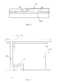
- FIG. 1 is an illustrative structural view of an array substrate according to one embodiment of the present disclosure
- FIG. 2-1 is an illustrative structural view of an array substrate according to another embodiment of the present disclosure.
- FIG. 2-2 is an illustrative structural view of the array substrate as illustrated in FIG. 2-1 , wherein a photosensitive structure is not formed on the array substrate;
- FIG. 2-3 is a top view of the array substrate as illustrated in FIG. 2-1 ;
- FIG. 2-4 is a equivalent schematic circuit diagram of the array substrate as illustrated in FIG. 2-1 ;
- FIG. 2-5 is an illustrative structural view of an array substrate according to another embodiment of the present disclosure.
- FIG. 3-1 is a flow chart of a manufacturing method of an array substrate according to one embodiment of the present disclosure
- FIG. 3-2 is an illustrative structural view of a base substrate manufactured by the manufacturing method according to the embodiment as illustrated in FIG. 3-1 ;
- FIG. 4-1 is a flow chart of a manufacturing method of an array substrate according to one embodiment of the present disclosure
- FIG. 4-2 to FIG. 4-7 are illustrative structural views of a base substrate manufactured by the manufacturing method according to the embodiment as illustrated in FIG. 4 - 1 ;
- FIG. 5-1 is a flow chart of a control method for an array substrate according to one embodiment of the present disclosure
- FIG. 5-2 is a flow chart of controlling display brightness in the control method for the array substrate according to the embodiment as illustrated in FIG. 5-1 ;
- FIG. 6 is a block diagram of a control assembly according to one embodiment of the present disclosure.
- FIG. 1 is an illustrative structural view of an array substrate according to one embodiment of the present disclosure.
- the array substrate comprising: a base substrate 110 ; a thin film transistor 120 formed on the base substrate 110 ; and at least one photosensitive structure 130 , formed on the base substrate 110 ; wherein the at least one photosensitive structure 130 is electrically connected with a drain electrode 121 of the thin film transistor 120 and is configured to sense light intensity outside.
- the array substrate further comprises a common electrode 140 , formed on the substrate 110 on which the thin film transistor 120 and the at least one photosensitive structure 130 are formed.
- light intensity outside is sensed by the photosensitive structure formed on the array substrate.
- light intensity outside is not required to be sensed by a light sensing unit mounted outside, as does conventional techniques, and cost for obtaining auto-brightness adjustment of display is reduced.
- FIG. 2-1 illustrate an illustrative structure view of an array substrate according to another embodiment of the present disclosure.
- the array substrate is a variant of the array substrate as illustrated in FIG. 1 , wherein a photosensitive structure comprises a photosensitive layer 131 and a photosensitive electrode 132 , which forms together the photosensitive structure 130 as illustrated in FIG. 1 .
- a photosensitive electrode 132 is formed on the base substrate 110 on which the thin film transistor 120 is formed, and the photosensitive electrode 132 is electrically connected with a drain electrode 121 of the thin film transistor 120 .
- the photosensitive layer 131 is formed on the photosensitive electrode 132 , and the common electrode 140 is formed on the photosensitive layer 131 .
- the photosensitive layer 131 may be formed in a region over the thin film transistor 120 , and the photosensitive layer 131 may not be formed in a region over the thin film transistor 120 , which is not limited herein. If the photosensitive layer 131 is formed in a region over the thin film transistor 120 , an insulating layer is formed between the thin film transistor 120 and the photosensitive layer 131 so as to protect the thin film transistor 120 .
- the photosensitive layer 131 is formed of a material comprising at least one of photosensitive resin and photosensitive polymer.
- a light emitting structure 150 is formed on the common electrode 140 .
- a pixel electrode 160 can be formed on the light emitting structure 150 .
- the pixel electrode 160 is electrically connected with a drain electrode 121 of the thin film transistor 120 .
- the light emitting structure 150 may be formed in a region over the thin film transistor 120 , and may not be formed in a region over the thin film transistor 120 , which is not limited in the present disclosure.
- the pixel electrode 160 can be electrically connected with the photosensitive electrode 132 via a through hole. As the photosensitive electrode 132 is electrically connected with the drain electrode 121 , the pixel electrode 160 can be electrically connected with the drain electrode 121 . And if the pixel electrode 160 is electrically connected with the photosensitive electrode, the pixel electrode 160 is not in contact with the photosensitive layer 131 .
- the light emitting structure 150 is a three-layered electroluminescence structure or a five-layered electroluminescence structure.
- the light emitting structure 150 is a three-layered electroluminescence structure, it comprises a cathode, an electroluminescence layer and an anode.
- the light emitting structure 150 is a five-layered electroluminescence structure, it comprises a cathode, an electroluminescence layer, an ion conductor layer, an ion storage layer and an anode.
- the photosensitive structure can be disposed in a portion of a pixel region. For example, pixels in any one to four columns are provided with a photosensitive structure, while other pixels are not provided with photosensitive structure.
- Structure of a portion of the array substrate which is not provided photosensitive structure is illustrated in FIG. 2-2 , wherein the pixel electrode 160 is directly electrically connected with the drain electrode 121 and the common electrode 140 is formed on the insulating layer 170 .
- a top view of the array substrate according to this embodiment of the present disclosure is illustrated in FIG.
- a common signal line 210 is connected with the common electrode 140 so as to supply electrical signals to the common electrode 140
- the data line 220 is electrically connected with the drain electrode of the thin film transistor 120 .
- FIG. 2-4 illustrates a equivalent schematic circuit diagram of the array substrate according to one embodiment of the present disclosure, wherein G is a gate electrode, S is a source electrode and D is a drain electrode, Cst refers to the capacitance between the pixel electrode and the common electrode, Cs refers to the capacitance between the photosensitive electrode and the common electrode, and the Cst is connected with the Cs in parallel.
- the Cst is included in conventional arts, while the array substrate further comprises a Cs with respect to the conventional arts, which enlarge the storage capacitance, thus facilitating holding voltage of the pixel, and mitigating defects in image quality due to leakage current (a current flowing through the thin film transistor when the thin film transistor is OFF).
- FIG. 2-5 illustrates structure of an array substrate according to one embodiment of the present disclosure, wherein shapes of a light emitting structure 150 and the photosensitive layer 131 are formed through a patterning process so as to make the pixel electrode 160 electrically connected with the photosensitive electrode 132 .
- the pixel electrode 160 and the photosensitive layer 131 are not formed over the thin film transistor 120 , and a portion of the photosensitive electrode 132 is not overlapped by the pixel electrode 160 and the photosensitive layer 131 . Then, the pixel electrode 160 formed on the light emitting structure 150 can be directly electrically connected with the photosensitive electrode 132 or the drain electrode 121 .
- a light emitting structure formed on the base substrate can obtain an effect that the array substrate can emit light itself.
- operation state of the array substrate comprising a photosensitive structure comprises a photo sensing stage and a display stage.
- Light intensity outside is sensed before displaying image, so as to adjust display brightness according to light intensity outside.
- the photo sensing stage has a very short duration, for example, several milliseconds, so as to not affect normal display.
- inputting signals to the source electrode of the thin film transistor is stopped.
- the photosensitive structure generates photocurrent under effect of the light from outside. Amplitude of the generated photocurrent is proportional to light intensity outside.
- the photocurrent can flow reversely (that is, flowing in a direction opposite to the direction of driving current), from the drain electrode to the source electrode.
- the light intensity outside can be determined on basis of the amplitude of the photocurrent, and the display brightness can be controlled on basis of the light intensity outside, such as controlling brightness of the backlight source.
- a photosensitive structure is formed on the array substrate so as to sense light intensity outside.
- it is not required to mount a photosensitive unit outside to sense light intensity outside, thus reducing cost of obtaining auto adjustment for display brightness.
- FIG. 3-1 is a flow chart of a manufacturing method of an array substrate according to one embodiment of the present disclosure, the manufacturing method comprising:
- a pattern comprising a common electrode 140 on the base substrate on which the thin film transistor and the at least one photosensitive structure are formed.
- FIG. 3-2 After forming a thin film transistor and at least one photosensitive structure on a base substrate, a structure of the base substrate is illustrated in FIG. 3-2 , wherein the thin film transistor 120 and the photosensitive structure 130 are formed on the base substrate 110 , and the photosensitive structure 130 is electrically connected with the drain electrode 121 of the thin film transistor 120 .
- the structure of the array substrate as illustrated in FIG. 1 is obtained.
- a photosensitive structure is formed on the array substrate and is configured to sense light intensity outside.
- light intensity outside is not required to be sensed by a light sensing unit mounted outside, as conventional techniques do, and cost for obtaining auto-brightness adjustment of display is reduced.
- FIG. 4-1 is a flow chart of a manufacturing method of an array substrate according to another embodiment of the present disclosure, the method comprising:
- a pattern comprising a photosensitive electrode on the base substrate on which the thin film transistor is formed, wherein the photosensitive electrode is electrically connected with a drain electrode of the thin film transistor;
- a patterning comprising a pixel electrode, wherein the pixel electrode is electrically connected with a drain electrode of the thin film transistor.
- the structure of the base substrate is illustrated in FIG. 4-2 , wherein the thin film transistor 120 and the insulating layer 170 are formed on the base substrate.
- the resultant structure of the base substrate is illustrated in FIG. 4-3 , wherein the photosensitive electrode 132 is electrically connected with the drain electrode 121 of the thin film transistor 120 .
- material for the photosensitive layer comprises at least one of photosensitive resin and photosensitive polymer.
- FIG. 4-4 After forming a photosensitive layer on the photosensitive electrode, the resultant structure of the base substrate is illustrated in FIG. 4-4 , wherein the photosensitive layer 131 is formed on the photosensitive electrode.
- an insulating layer (not shown in the FIG. 4-4 ) can be formed between the thin film transistor and the photosensitive layer 131 so as to protect the thin film transistor 120 .
- the photosensitive layer 131 is not formed on the thin film transistor 120 .
- the pixel electrode can be electrically connected with the photosensitive electrode 132 via a through hole.
- FIG. 4-5 the resultant structure of the array substrate is illustrated in FIG. 4-5 , wherein the same reference signs refer to the similar structure as illustrated in FIG. 4-4 .
- the common electrode is formed on the photosensitive layer.
- the light emitting structure can be a three-layered electroluminescence structure or a five-layered electroluminescence structure.
- the light emitting structure is a three-layered electroluminescence structure, it comprises a cathode, an electroluminescence layer, and an anode. And if the light emitting structure is a five-layered electroluminescence structure, it comprises a cathode, a electroluminescence layer, an ion conductor layer, an ion storage layer and an anode.
- the resultant structure of the array substrate is as illustrated in FIG. 4-6 , wherein the light emitting structure 160 is formed on the common electrode 140 .
- the pixel electrode is electrically connected with the photosensitive electrode via a through hole.
- a second through hole k 2 is formed in the light emitting layer, the radius of the second through hole k 2 is less than the radius of the first through hole k 1 .
- the resultant structure of the base substrate is as illustrated in FIG. 2-1 .
- the radius of the second through hole k 2 is less than the radius of the first through hole k 1 , the pixel electrode 160 will not be in contact with the photosensitive layer 131 , thus mutual influence between the pixel electrode 160 and the photosensitive layer 131 .
- a light emitting structure is formed on the base substrate, thus the array substrate can emit light itself.
- a photosensitive structure is formed on the array substrate and is configured to sense light intensity outside.
- light intensity outside is not required to be sensed by a light sensing unit mounted outside, as conventional techniques do, and cost for obtaining auto-brightness adjustment of display is reduced.
- FIG. 5-1 is a flow chart of a control method for an array substrate according to one embodiment of the present disclosure, the method is adapted to a control assembly, which is configured to control the array substrate according to the embodiment as illustrated in FIG. 1 , or to control the array substrate according to the embodiment as illustrated in FIG. 2 , the array substrate comprising a thin film transistor, a photosensitive structure, and a common electrode, wherein the method comprises:
- control assembly stopping inputting a signal to a source electrode of the thin film transistor, the photosensitive structure configured to sense light intensity outside and generate photocurrent;
- control assembly receiving the photocurrent which pass through the drain electrode and the source electrode of the thin film transistor under effect of the common electrode;
- control assembly controlling display brightness according to amplitude of the photocurrent.
- the photocurrent generated by the photosensitive structure can flow reversely into the control assembly through the source electrode.
- period of stopping inputting signals to the source electrode of the thin film transistor can be taken as a photosensitive stage and other periods can be taken as a display stage.
- the photosensitive stage can be very short (for example, several milliseconds), thus, normal display will not be affected.
- the common electrode can be applied a preset negative voltage.
- control assembly After receiving the photocurrent, the control assembly can sense light intensity outside at present on basis of the photocurrent, and control display brightness according to the light intensity outside, for example, by controlling brightness of the backlight source.
- the array substrate further comprises a light emitting structure and a pixel electrode.
- control assembly controlling the display brightness according to the photocurrent can comprise:
- control assembly generating a control signal according to the photocurrent
- control assembly inputting the control signal to the source electrode of the thin film transistor, the control signal conducted by the thin film transistor to the drain electrode and flowing to the pixel electrode, and the light-emitting structure emitting light under effect of the pixel electrode and the common electrode.
- the control assembly can directly generate a control signal for controlling the light emitting structure, which can make the light emitting structure emit light with required brightness (for example, a brightness suitable for human eyes).
- control assembly just needs to output two timing signals (one for controlling the photosensitive stage, and the other for controlling the display stage).
- the control assembly can be provided with two Electrically Erasable Programmable Read-Only Memories (EEPROM), which are configured to output timing signals for controlling the photosensitive stage and the display stage respectively.
- EEPROM Electrically Erasable Programmable Read-Only Memories
- the effect of adjusting display brightness by controlling the array substrate is obtained through controlling light emitted from the light emitting structure disposed on the array substrate.
- a photosensitive structure is formed on the array substrate and is configured to sense light intensity outside.
- light intensity outside is not required to be sensed by a light sensing unit mounted outside, as conventional techniques do, and cost for obtaining auto-brightness adjustment of display is reduced.
- FIG. 6 illustrates a control assembly according to an embodiment of the present disclosure.
- the control assembly is configured to control the array substrate according to the embodiment illustrated in FIG. 1 or the array substrate according to the embodiment illustrated in FIG. 2-1 .
- the array substrate can comprise a thin film transistor, a photosensitive structure and a common electrode.
- the control assembly comprises:
- a stopping module 610 configured to stop inputting a signal to a source electrode of the thin film transistor, the photosensitive structure configured to sense light intensity outside and generate a photocurrent;
- a receiving module 620 configured to receive the photocurrent flowing through a drain electrode and the source electrode of the thin film transistor under effect of the common electrode;
- control module 630 configured to control display brightness on basis of the photocurrent.
- control module 630 is configured to generate a control signal on basis of the photocurrent and input the control signal to the source electrode of the thin film transistor, and then, the control signal is conducted to the drain electrode of the thin film transistor and flows into the pixel electrode, the light emitting structure emits light under effect of a pixel electrode and the common electrode.
- control assembly controls the light emitting structure disposed on the array substrate to emit light, thus achieving an effect of adjusting display brightness by controlling the array substrate.
- a photosensitive structure is formed on the array substrate and is configured to sense light intensity outside.
- light intensity outside is not required to be sensed by a light sensing unit mounted outside, as conventional techniques do, and cost for obtaining auto-brightness adjustment of display is reduced.
- At least one embodiment of the present disclosure further provides a display device, which comprises the array substrate according to the embodiment illustrated in FIG. 1 or the array substrate according to the embodiment illustrated in FIG. 2-1 .
- At least one embodiment of the present disclosure further provides a display device, which comprises the control assembly as illustrated in FIG. 6 .
Abstract
Description
| Reference Signs: |
| 101 |
120 |
||
| 121 drain electrode of |
130 | ||
| transistor | structure | ||
| 131 |
132 | ||
| electrode | |||
| 140 |
150 | ||
| structure | |||
| 160 |
170 insulating layer | ||
| G-gate electrode S-source electrode | D-drain electrode | ||
Claims (2)
Priority Applications (1)
| Application Number | Priority Date | Filing Date | Title |
|---|---|---|---|
| US16/130,208 US10629164B2 (en) | 2015-06-10 | 2018-09-13 | Array substrate, manufacturing method thereof, control method, control assembly, and display device |
Applications Claiming Priority (3)
| Application Number | Priority Date | Filing Date | Title |
|---|---|---|---|
| CN201510315475.4A CN104867948B (en) | 2015-06-10 | 2015-06-10 | Array base palte and its manufacture method, control method, control assembly and display device |
| CN201510315475.4 | 2015-06-10 | ||
| CN201510315475 | 2015-06-10 |
Related Child Applications (1)
| Application Number | Title | Priority Date | Filing Date |
|---|---|---|---|
| US16/130,208 Division US10629164B2 (en) | 2015-06-10 | 2018-09-13 | Array substrate, manufacturing method thereof, control method, control assembly, and display device |
Publications (2)
| Publication Number | Publication Date |
|---|---|
| US20160365069A1 US20160365069A1 (en) | 2016-12-15 |
| US10102822B2 true US10102822B2 (en) | 2018-10-16 |
Family
ID=53913665
Family Applications (2)
| Application Number | Title | Priority Date | Filing Date |
|---|---|---|---|
| US15/176,742 Active US10102822B2 (en) | 2015-06-10 | 2016-06-08 | Array substrate, manufacturing method thereof, control method, control assembly, and display device |
| US16/130,208 Active US10629164B2 (en) | 2015-06-10 | 2018-09-13 | Array substrate, manufacturing method thereof, control method, control assembly, and display device |
Family Applications After (1)
| Application Number | Title | Priority Date | Filing Date |
|---|---|---|---|
| US16/130,208 Active US10629164B2 (en) | 2015-06-10 | 2018-09-13 | Array substrate, manufacturing method thereof, control method, control assembly, and display device |
Country Status (2)
| Country | Link |
|---|---|
| US (2) | US10102822B2 (en) |
| CN (1) | CN104867948B (en) |
Families Citing this family (6)
| Publication number | Priority date | Publication date | Assignee | Title |
|---|---|---|---|---|
| CN107065328A (en) * | 2017-05-23 | 2017-08-18 | 京东方科技集团股份有限公司 | A kind of dot structure, display panel, display device and pixel structure preparation method |
| CN109309105A (en) * | 2017-07-26 | 2019-02-05 | Tcl集团股份有限公司 | Device of light conversion and preparation method thereof, infrared imaging device |
| CN107644892B (en) | 2017-09-15 | 2020-04-14 | 京东方科技集团股份有限公司 | OLED light source, display device and preparation method |
| CN109147698B (en) * | 2018-09-12 | 2020-04-17 | 重庆惠科金渝光电科技有限公司 | Display device and automatic screen brightness adjusting method thereof |
| CN110780502A (en) * | 2019-10-31 | 2020-02-11 | 南京中电熊猫平板显示科技有限公司 | Photosensitive device, array substrate, display device and brightness adjusting method of display device |
| CN114420067A (en) * | 2022-01-29 | 2022-04-29 | 联想(北京)有限公司 | Display panel and display control method |
Citations (8)
| Publication number | Priority date | Publication date | Assignee | Title |
|---|---|---|---|---|
| US20050156261A1 (en) | 2003-12-24 | 2005-07-21 | Sanyo Electric Co., Ltd. | Optical sensor and display |
| CN1645631A (en) | 2003-12-24 | 2005-07-27 | 三洋电机株式会社 | Optical sensor and display |
| US20070096636A1 (en) * | 2005-10-28 | 2007-05-03 | Samsung Electronics Co., Ltd | Organic light emitting diode display and method of manufacturing the same |
| JP2008191822A (en) | 2007-02-02 | 2008-08-21 | Hannstar Display Corp | Light receiving element and liquid crystal display device |
| CN102354695A (en) | 2011-02-11 | 2012-02-15 | 友达光电股份有限公司 | Display and manufacturing method thereof |
| CN102622970A (en) | 2011-01-28 | 2012-08-01 | 美国博通公司 | Backlight module and control method thereof |
| CN102667905A (en) | 2009-11-30 | 2012-09-12 | 夏普株式会社 | Display device |
| US20150145840A1 (en) * | 2013-11-26 | 2015-05-28 | Samsung Display Co., Ltd. | Pixel circuit and display device having the same |
Family Cites Families (1)
| Publication number | Priority date | Publication date | Assignee | Title |
|---|---|---|---|---|
| US20070109239A1 (en) * | 2005-11-14 | 2007-05-17 | Den Boer Willem | Integrated light sensitive liquid crystal display |
-
2015
- 2015-06-10 CN CN201510315475.4A patent/CN104867948B/en active Active
-
2016
- 2016-06-08 US US15/176,742 patent/US10102822B2/en active Active
-
2018
- 2018-09-13 US US16/130,208 patent/US10629164B2/en active Active
Patent Citations (11)
| Publication number | Priority date | Publication date | Assignee | Title |
|---|---|---|---|---|
| US20050156261A1 (en) | 2003-12-24 | 2005-07-21 | Sanyo Electric Co., Ltd. | Optical sensor and display |
| CN1645631A (en) | 2003-12-24 | 2005-07-27 | 三洋电机株式会社 | Optical sensor and display |
| US20070096636A1 (en) * | 2005-10-28 | 2007-05-03 | Samsung Electronics Co., Ltd | Organic light emitting diode display and method of manufacturing the same |
| JP2008191822A (en) | 2007-02-02 | 2008-08-21 | Hannstar Display Corp | Light receiving element and liquid crystal display device |
| CN102667905A (en) | 2009-11-30 | 2012-09-12 | 夏普株式会社 | Display device |
| US20120293475A1 (en) | 2009-11-30 | 2012-11-22 | Sharp Kabushiki Kaisha | Display device |
| CN102622970A (en) | 2011-01-28 | 2012-08-01 | 美国博通公司 | Backlight module and control method thereof |
| US20120194493A1 (en) | 2011-01-28 | 2012-08-02 | Broadcom Corporation | Apparatus and Method for Using an LED for Backlighting and Ambient Light Sensing |
| CN102354695A (en) | 2011-02-11 | 2012-02-15 | 友达光电股份有限公司 | Display and manufacturing method thereof |
| US20120205646A1 (en) | 2011-02-11 | 2012-08-16 | Au Optronics Corporation | Display with photo sensor and manufacturing method thereof |
| US20150145840A1 (en) * | 2013-11-26 | 2015-05-28 | Samsung Display Co., Ltd. | Pixel circuit and display device having the same |
Non-Patent Citations (1)
| Title |
|---|
| The First Chinese Office Action dated May 18, 2017, Appln. No. 201510315475.4. |
Also Published As
| Publication number | Publication date |
|---|---|
| CN104867948B (en) | 2018-01-19 |
| CN104867948A (en) | 2015-08-26 |
| US20190012984A1 (en) | 2019-01-10 |
| US10629164B2 (en) | 2020-04-21 |
| US20160365069A1 (en) | 2016-12-15 |
Similar Documents
| Publication | Publication Date | Title |
|---|---|---|
| US10629164B2 (en) | Array substrate, manufacturing method thereof, control method, control assembly, and display device | |
| CN108831912B (en) | OLED array substrate, method for manufacturing OLED array substrate, OLED pixel circuit and display device | |
| EP3522145A1 (en) | Display device and method for controlling brightness of display device | |
| JP4007390B2 (en) | Electro-optical device and electronic apparatus | |
| US9715851B1 (en) | Display panel, method of manufacturing the same, display device and method of controlling the display device | |
| US9324276B2 (en) | Liquid crystal display device and method for automatically controlling brightness | |
| US20180059404A1 (en) | Electronic device and method of controlling light transmittance of the same | |
| US11475855B2 (en) | Backlight module and display device | |
| US9076372B2 (en) | Display device and light adjusting method thereof | |
| CN110071164B (en) | Display substrate, brightness adjusting method thereof and display device | |
| US9330604B2 (en) | Organic light-emitting diode pixel circuit, drive method thereof, and display device | |
| CN108417172A (en) | Array substrate, display screen and display device | |
| US20180088420A1 (en) | Discharge circuit, array substrate, liquid crystal display panel and display device | |
| US20190229169A1 (en) | Display panel and manufacturing method therefor, and display apparatus | |
| US11156868B2 (en) | Charge release circuit and driving method therefor, and display device | |
| US10649250B2 (en) | Photosensitive detection module, light source module and electrophoresis display apparatus | |
| CN112331141A (en) | OLED display panel and display device | |
| CN107785403B (en) | Display panel and display device | |
| JP4656082B2 (en) | Electro-optical device and electronic apparatus | |
| US11329259B2 (en) | Display panel comprising capacitor structure between first plate and second plate, and method of fabricating thereof | |
| US11157112B2 (en) | Display panel, display device and manufacturing method of display panel | |
| US20200328261A1 (en) | Organic light emitting diode display device | |
| WO2021129632A1 (en) | Electronic device, control method therefor, and computer readable storage medium | |
| CN114783345A (en) | Pixel driving circuit, display module, display device and intelligent watch | |
| US20160027361A1 (en) | Display device and driving method thereof, manufacturing method of array substrate |
Legal Events
| Date | Code | Title | Description |
|---|---|---|---|
| AS | Assignment |
Owner name: BOE TECHNOLOGY GROUP CO., LTD., CHINA Free format text: ASSIGNMENT OF ASSIGNORS INTEREST;ASSIGNOR:BAO, ZHIYING;REEL/FRAME:038917/0682 Effective date: 20160307 Owner name: BOE TECHNOLOGY GROUP CO., LTD., CHINA Free format text: ASSIGNMENT OF ASSIGNORS INTEREST;ASSIGNOR:JIANG, WENBO;REEL/FRAME:038917/0670 Effective date: 20160307 Owner name: BEIJING BOE OPTOELECTRONICS TECHNOLOGY CO., LTD., Free format text: ASSIGNMENT OF ASSIGNORS INTEREST;ASSIGNOR:BAO, ZHIYING;REEL/FRAME:038917/0682 Effective date: 20160307 Owner name: BEIJING BOE OPTOELECTRONICS TECHNOLOGY CO., LTD., Free format text: ASSIGNMENT OF ASSIGNORS INTEREST;ASSIGNOR:JIANG, WENBO;REEL/FRAME:038917/0670 Effective date: 20160307 Owner name: BEIJING BOE OPTOELECTRONICS TECHNOLOGY CO., LTD., Free format text: ASSIGNMENT OF ASSIGNORS INTEREST;ASSIGNOR:WANG, SHIJUN;REEL/FRAME:038917/0742 Effective date: 20160307 Owner name: BOE TECHNOLOGY GROUP CO., LTD., CHINA Free format text: ASSIGNMENT OF ASSIGNORS INTEREST;ASSIGNOR:WANG, SHIJUN;REEL/FRAME:038917/0742 Effective date: 20160307 Owner name: BOE TECHNOLOGY GROUP CO., LTD., CHINA Free format text: ASSIGNMENT OF ASSIGNORS INTEREST;ASSIGNOR:LV, ZHENHUA;REEL/FRAME:038918/0078 Effective date: 20160307 Owner name: BEIJING BOE OPTOELECTRONICS TECHNOLOGY CO., LTD., Free format text: ASSIGNMENT OF ASSIGNORS INTEREST;ASSIGNOR:LV, ZHENHUA;REEL/FRAME:038918/0078 Effective date: 20160307 |
|
| STCF | Information on status: patent grant |
Free format text: PATENTED CASE |
|
| MAFP | Maintenance fee payment |
Free format text: PAYMENT OF MAINTENANCE FEE, 4TH YEAR, LARGE ENTITY (ORIGINAL EVENT CODE: M1551); ENTITY STATUS OF PATENT OWNER: LARGE ENTITY Year of fee payment: 4 |