US10097272B2 - Optical module - Google Patents
Optical module Download PDFInfo
- Publication number
- US10097272B2 US10097272B2 US15/294,572 US201615294572A US10097272B2 US 10097272 B2 US10097272 B2 US 10097272B2 US 201615294572 A US201615294572 A US 201615294572A US 10097272 B2 US10097272 B2 US 10097272B2
- Authority
- US
- United States
- Prior art keywords
- optical module
- laser
- laser receiver
- master control
- control chip
- Prior art date
- Legal status (The legal status is an assumption and is not a legal conclusion. Google has not performed a legal analysis and makes no representation as to the accuracy of the status listed.)
- Expired - Fee Related
Links
- 230000003287 optical effect Effects 0.000 title claims abstract description 75
- 210000000078 claw Anatomy 0.000 claims description 11
- 238000003860 storage Methods 0.000 claims description 8
- 239000006260 foam Substances 0.000 claims description 2
- 238000010586 diagram Methods 0.000 description 9
- 230000035945 sensitivity Effects 0.000 description 7
- JAYCNKDKIKZTAF-UHFFFAOYSA-N 1-chloro-2-(2-chlorophenyl)benzene Chemical compound ClC1=CC=CC=C1C1=CC=CC=C1Cl JAYCNKDKIKZTAF-UHFFFAOYSA-N 0.000 description 6
- 101100084627 Neurospora crassa (strain ATCC 24698 / 74-OR23-1A / CBS 708.71 / DSM 1257 / FGSC 987) pcb-4 gene Proteins 0.000 description 6
- 230000008033 biological extinction Effects 0.000 description 6
- 238000013461 design Methods 0.000 description 6
- 239000013307 optical fiber Substances 0.000 description 4
- 230000005540 biological transmission Effects 0.000 description 3
- 238000004891 communication Methods 0.000 description 2
- 230000009977 dual effect Effects 0.000 description 2
- 238000012986 modification Methods 0.000 description 2
- 230000004048 modification Effects 0.000 description 2
- 230000005855 radiation Effects 0.000 description 2
- 230000008859 change Effects 0.000 description 1
- 238000011161 development Methods 0.000 description 1
- 238000003745 diagnosis Methods 0.000 description 1
- 239000000428 dust Substances 0.000 description 1
- 230000000694 effects Effects 0.000 description 1
- 238000005516 engineering process Methods 0.000 description 1
- 239000000835 fiber Substances 0.000 description 1
- 238000004519 manufacturing process Methods 0.000 description 1
- 238000000034 method Methods 0.000 description 1
- 230000008569 process Effects 0.000 description 1
- 230000004044 response Effects 0.000 description 1
- 238000004904 shortening Methods 0.000 description 1
- 230000008054 signal transmission Effects 0.000 description 1
- 238000002834 transmittance Methods 0.000 description 1
Images


Classifications
-
- H—ELECTRICITY
- H04—ELECTRIC COMMUNICATION TECHNIQUE
- H04B—TRANSMISSION
- H04B10/00—Transmission systems employing electromagnetic waves other than radio-waves, e.g. infrared, visible or ultraviolet light, or employing corpuscular radiation, e.g. quantum communication
- H04B10/40—Transceivers
-
- G—PHYSICS
- G02—OPTICS
- G02B—OPTICAL ELEMENTS, SYSTEMS OR APPARATUS
- G02B6/00—Light guides; Structural details of arrangements comprising light guides and other optical elements, e.g. couplings
-
- G—PHYSICS
- G02—OPTICS
- G02B—OPTICAL ELEMENTS, SYSTEMS OR APPARATUS
- G02B6/00—Light guides; Structural details of arrangements comprising light guides and other optical elements, e.g. couplings
- G02B6/24—Coupling light guides
- G02B6/42—Coupling light guides with opto-electronic elements
- G02B6/4201—Packages, e.g. shape, construction, internal or external details
- G02B6/4274—Electrical aspects
- G02B6/428—Electrical aspects containing printed circuit boards [PCB]
-
- G—PHYSICS
- G02—OPTICS
- G02B—OPTICAL ELEMENTS, SYSTEMS OR APPARATUS
- G02B6/00—Light guides; Structural details of arrangements comprising light guides and other optical elements, e.g. couplings
- G02B6/24—Coupling light guides
- G02B6/42—Coupling light guides with opto-electronic elements
- G02B6/4296—Coupling light guides with opto-electronic elements coupling with sources of high radiant energy, e.g. high power lasers, high temperature light sources
-
- H—ELECTRICITY
- H04—ELECTRIC COMMUNICATION TECHNIQUE
- H04B—TRANSMISSION
- H04B10/00—Transmission systems employing electromagnetic waves other than radio-waves, e.g. infrared, visible or ultraviolet light, or employing corpuscular radiation, e.g. quantum communication
- H04B10/50—Transmitters
- H04B10/501—Structural aspects
- H04B10/503—Laser transmitters
-
- H—ELECTRICITY
- H04—ELECTRIC COMMUNICATION TECHNIQUE
- H04B—TRANSMISSION
- H04B10/00—Transmission systems employing electromagnetic waves other than radio-waves, e.g. infrared, visible or ultraviolet light, or employing corpuscular radiation, e.g. quantum communication
- H04B10/60—Receivers
-
- H—ELECTRICITY
- H04—ELECTRIC COMMUNICATION TECHNIQUE
- H04B—TRANSMISSION
- H04B10/00—Transmission systems employing electromagnetic waves other than radio-waves, e.g. infrared, visible or ultraviolet light, or employing corpuscular radiation, e.g. quantum communication
- H04B10/60—Receivers
- H04B10/66—Non-coherent receivers, e.g. using direct detection
- H04B10/67—Optical arrangements in the receiver
-
- H—ELECTRICITY
- H04—ELECTRIC COMMUNICATION TECHNIQUE
- H04B—TRANSMISSION
- H04B10/00—Transmission systems employing electromagnetic waves other than radio-waves, e.g. infrared, visible or ultraviolet light, or employing corpuscular radiation, e.g. quantum communication
- H04B10/60—Receivers
- H04B10/66—Non-coherent receivers, e.g. using direct detection
- H04B10/69—Electrical arrangements in the receiver
-
- G—PHYSICS
- G02—OPTICS
- G02B—OPTICAL ELEMENTS, SYSTEMS OR APPARATUS
- G02B6/00—Light guides; Structural details of arrangements comprising light guides and other optical elements, e.g. couplings
- G02B6/24—Coupling light guides
- G02B6/42—Coupling light guides with opto-electronic elements
- G02B6/4201—Packages, e.g. shape, construction, internal or external details
- G02B6/4274—Electrical aspects
Definitions
- the present application relates to optical communication technologies and, in particular, to an optical module.
- optical modules are globally demanded in huge volume, which makes cost control of optical modules particularly important in the process of developing and manufacturing the optical modules.
- Some embodiments of the present application provide an optical module, including: a master control chip, a laser transmitter and a laser receiver; the laser transmitter and the laser receiver being connected to the master control chip, respectively; where the laser receiver includes: a PIN photodiode, a trans-impedance amplifier with a transimpedance of no less than 43K ohms, a lens and a shell; the PIN photodiode being electrically connected to the trans-impedance amplifier; the PIN photodiode, the trans-impedance amplifier and the lens being encapsulated within the shell in a manner of transistor out-line; and the lens being coated with an antireflection film.
- FIG. 1 is a schematic diagram illustrating a circuit structure of an optical module according to some embodiments of the present application
- FIG. 2 is a schematic structural diagram of a laser receiver of FIG. 1 ;
- FIG. 3 is a sectional view of the laser receiver of FIG. 2 taken along line A-A;
- FIG. 4 is a perspective view illustrating an optical module according to some embodiments of the present application.
- FIG. 5 is an exploded view illustrating an optical module according to some embodiments of the present application.
- FIG. 6 is a schematic structural diagram of a BOSA of FIG. 5 ;
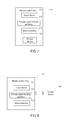
- FIG. 7 is a schematic structural diagram of a master control chip according to some embodiments of the present application.
- FIG. 8 is a schematic structural diagram of a master control chip according to some other embodiments of the present application.
- FIG. 9 is a schematic structural diagram of an optical module according to some embodiments of the present application.
- An optical module provided in some embodiments of the present application may be applied to an optical network unit (ONU) in a gigabit capable passive optical network (GPON) to achieve high data rate transmission over long distance.
- the optical module may also be applied to an ONU in other passive optical networks (PON), such as Ethernet passive optical network (EPON), for transmitting signals through optical fibers.
- PON passive optical networks
- EPON Ethernet passive optical network
- FIG. 1 is a schematic diagram illustrating a circuit structure of an optical module according to some embodiments of the present application
- FIG. 2 is a schematic structural diagram of a laser receiver of FIG. 1
- FIG. 3 is a sectional view of the laser receiver of FIG. 2 taken along line A-A. As shown in FIGS.
- an optical module provided in some embodiments of the present application includes a master control chip 10 , a laser transmitter 20 and a laser receiver 30 , the laser transmitter 20 and the laser receiver 30 being connected to the master control chip 10 , respectively; where the laser receiver 30 includes a PIN photodiode 31 , a trans-impedance amplifier (TIA) 32 with a transimpedance of no less than 43K ohms, a lens 33 and a shell 34 ; the PIN photodiode 31 being electrically connected to the TIA 32 ; the PIN photodiode 31 , the TIA 32 and the lens 33 being encapsulated within the shell 34 in a manner of transistor out-line; and the lens 33 being coated with an antireflection film 33 ′.
- TIA trans-impedance amplifier
- the master control chip 10 may be a highly integrated three-in-one chip in which a laser driver 101 , a receipt signal limiting amplifier 102 and a microcontroller 103 are integrated.
- a storage device 104 of small capacity may be integrated in the master control chip 10 , as shown in FIG. 7 ; or the master control chip 10 may be connected to an external storage device 104 ′, such as an electrically erasable programmable read-only memory (EEPROM), through a bus, as shown in FIG. 8 .
- the laser transmitter 20 may convert an electrical signal from the master control chip 10 into an optical signal to be transmitted through an optical fiber.
- the laser receiver 30 may convert an optical signal from the optical fiber into an electrical signal to be transmitted to the master control chip 10 .
- the laser transmitter 20 and the laser receiver 30 may be encapsulated in a transmitter optical subassembly (TOSA) 91 and a receiver optical subassembly (ROSA) 90 , respectively, as shown in FIG. 9 .
- TOSA transmitter optical subassembly
- ROSA receiver optical subassembly
- the laser transmitter 20 and the laser receiver 30 may be encapsulated together in a bi-directional optical sub-assembly (BOSA).
- BOSA bi-directional optical sub-assembly
- the laser transmitter 20 may be configured to automatically control its optical power and extinction ratio by using closed-loop design of optical power, dual closed-loop design of optical power and extinction ratio, or open-loop design.
- closed-loop design of optical power a backlight diode and a laser diode (LD) are integrated in the laser transmitter 20 , and the master control chip 10 automatically controls the power according to a bias current collected from the backlight diode, so as to prevent unstable optical power caused by slope efficiency changes of the LD as the temperature changes.
- LD laser diode
- a first lookup table (containing the correlation between a modulation current and the temperature) is pre-generated based on characteristics of the LD and stored in a storage device, and the table is queried according to the temperature, so that the extinction ratio is maintained stable under different temperatures.
- the master control chip 10 provides automatic compensation according to changes of a bias current collected from the backlight diode and a modulation current collected from the LD, so that both the optical power and the extinction ratio are kept stable.
- a second lookup table (containing the correlation between the bias current and the temperature) needs to be pre-generated based on characteristics of the laser transmitter 20 and stored in a storage device, and the table is queried according to the temperature, so that both the optical power and the extinction ratio are maintained stable under different temperatures.
- the master control chip 10 may implement direct control over the laser driver 101 through an internal register, so as to achieve fast control response.
- the register may timely control and change the laser driver according to different conditions of a continuously tracked ONU temperature, a supply voltage, a laser bias current and a modulation current, so as to ensure reliable operation of the optical module.
- the master control chip 10 samples a monitored current output from the laser receiver 30 , so that digital diagnosis may be enabled on the optical module.
- a temperature sensor and an internal analog-to-digital converter (ADC) may be integrated in the master control chip 10 to convert collected data, so that the temperature and voltage can be monitored.
- ADC analog-to-digital converter
- the bandwidth of the PIN photodiode 31 may be 2.5G, 10G or the like, and preferably 10G in this embodiment for ensuring sufficient bandwidth.
- the trans-impedance amplifier 32 is a high gain TIA with a transimpedance of no less than 43K ohms, e.g. a TIA 32 with a transimpedance of 51K ohms for ensuring better gain effect.
- the PIN photodiode 31 , the TIA 32 and the lens 33 of the laser receiver 30 are encapsulated within the shell 34 in a manner of transistor out-line (TO), where the lens 33 may be hemispherical.
- TO transistor out-line
- an anti-reflection film for a corresponding wave band may be coated on the lens 102 , so as to reduce reflection of the received light, increase transmitted light, and hence increase sensitivity.
- the antireflection film has a transmittance of more than 98%.
- the high gain TIA 32 with a transimpedance of no less than 43K ohms can sufficiently amplify a weak electrical signal converted by the PIN photodiode 31 , which increases the sensitivity of the laser receiver 30 , thereby meeting the requirement of GPONs for long distances. That is, in some embodiments of the present application, the PIN photodiode 31 combined with a super TIA may be used to provide transmission with high sensitivity and long distance in the GPONs.
- an optical module includes: a master control chip, a laser transmitter and a laser receiver, the laser transmitter and the laser receiver being connected to the master control chip, respectively, where the laser receiver is embodied as a PIN photodiode combined with a high gain trans-impedance amplifier of no less than 43K ohms transimpedance.
- the optical module can provide transmission with high sensitivity and long distance in the GPONs while effectively lowering the cost.
- an antireflection film is coated on a lens of the laser receiver to reduce reflection of received light, increase transmitted light, thereby further increasing sensitivity.
- FIG. 4 is a perspective view illustrating an optical module according to some embodiments of the present application
- FIG. 5 is an exploded view illustrating an optical module according to some embodiments of the present application. Additionally, some embodiments of the present application are described by taking a laser transmitter 20 and a laser receiver 30 being encapsulated in a BOSA 1 as an example.
- FIG. 6 is a schematic structural diagram of a BOSA of FIG. 5 .
- a conductive gasket 3 is provided between a laser receiver 30 (which is contained in a BOSA 1 ) and a housing 2 of the optical module.
- the conductive gasket 3 may be conductive foam or conductive rubber etc., and be provided between the laser receiver 30 of the BOSA 1 and the housing 2 (i.e. between the BOSA 1 and the housing 2 shown in FIG. 4 ), so that the laser receiver 30 is sufficiently in touch with the housing 2 so as to shorten the length of a ground loop, maintain a stable ground level reference, avoid introducing a ground noise which will interfere with a received high-frequency signal, thereby further improving sensitivity.
- the master control chip 10 is provided on a printed circuit board (PCB) 4 of the optical module, the PCB 4 being electrically connected to the laser transmitter 20 and the laser receiver 30 .
- PCB printed circuit board
- the optical module may be of a pluggable structure or a pigtail structure. In some embodiments of the present application, the optical module is described by taking a pluggable structure as an example.
- the PCB may be a two-layer board, a four-layer board or a six-layer board, etc.
- the PCB 4 may be designed as a four-layer board to lower cost.
- a complete ground plane can be provided on the second layer to minimize the length of the ground loop, so as to improve the capacity of resisting interference and reduce radiation.
- the PCB 4 may be designed as a two-layer board to lower the cost.
- a high rate signal line for signal reception may be copper-plated on both its upper and lower sides, and a ground plane may be laid to include evenly distributed vias so as to minimize the length of the ground loop, which helps improving the capacity of resisting interference and reducing radiation.
- the optical module further includes a pin assembly 5 , a bracket 6 , a claw 7 , and a tail plug 8 , where one end of the pin assembly 5 is welded on the PCB 4 and the other end is provided passing through the bracket 6 , the laser transmitter 20 and the laser receiver 30 are fixed between the housing 2 and the bracket 6 by the claw 7 , and one end of the tail plug 8 is provided within the claw 7 .
- the pin assembly 5 may include 20 PINs, with one end welded on the PCB 4 , and the other end passing through the bracket 6 to connect to a main board to allow for signal transmission.
- One end of the BOSA 1 is welded on the PCB 4 and the other end is fixed in the claw 7 which is clamped between the housing 2 and the bracket 6 , so as to fix the BOSA 1 within a tube formed by the housing 2 and the bracket 6 .
- the outward facing end of the claw 7 is plugged by the tail plug 8 to ward off dust.
- a conductive gasket is provided between a laser receiver and a housing so as to enable the laser receiver to be sufficiently in touch with the housing, thereby shortening the length of a ground loop and improving sensitivity.
Landscapes
- Physics & Mathematics (AREA)
- Electromagnetism (AREA)
- Engineering & Computer Science (AREA)
- Computer Networks & Wireless Communication (AREA)
- Signal Processing (AREA)
- Optics & Photonics (AREA)
- General Physics & Mathematics (AREA)
- Semiconductor Lasers (AREA)
- Optical Couplings Of Light Guides (AREA)
Abstract
Description
| Description of reference signs: |
| 10-Master control chip; | 20-Laser transmitter; |
| 30-Laser receiver; | |
| 31-PIN photodiode; | 32-TIA; |
| 33-Lens; | 33-Antireflection film |
| 34-Shell; | |
| 1-BOSA; | 2-Housing; |
| 3-Conductive gasket; | 4-PCB; |
| 5-Pin assembly; | 6-BracketBracket; |
| 7-Claw; | 8-Tail plug; |
| 101-Laser driver; | 102-Receipt signal limiting amplifier; |
| 103-Microcontroller; | 104-Internal storage device; |
| 104-External storage device; | |
| 90-ROSA; | 91-TOSA. |
Claims (14)
Priority Applications (1)
| Application Number | Priority Date | Filing Date | Title |
|---|---|---|---|
| US16/104,853 US10516484B2 (en) | 2016-03-28 | 2018-08-17 | Optical module |
Applications Claiming Priority (3)
| Application Number | Priority Date | Filing Date | Title |
|---|---|---|---|
| CN201610184340.3 | 2016-03-28 | ||
| CN201610184340.3A CN105871471A (en) | 2016-03-28 | 2016-03-28 | Optical module |
| CN201610184340 | 2016-03-28 |
Related Child Applications (1)
| Application Number | Title | Priority Date | Filing Date |
|---|---|---|---|
| US16/104,853 Division US10516484B2 (en) | 2016-03-28 | 2018-08-17 | Optical module |
Publications (2)
| Publication Number | Publication Date |
|---|---|
| US20170279534A1 US20170279534A1 (en) | 2017-09-28 |
| US10097272B2 true US10097272B2 (en) | 2018-10-09 |
Family
ID=56625212
Family Applications (2)
| Application Number | Title | Priority Date | Filing Date |
|---|---|---|---|
| US15/294,572 Expired - Fee Related US10097272B2 (en) | 2016-03-28 | 2016-10-14 | Optical module |
| US16/104,853 Active US10516484B2 (en) | 2016-03-28 | 2018-08-17 | Optical module |
Family Applications After (1)
| Application Number | Title | Priority Date | Filing Date |
|---|---|---|---|
| US16/104,853 Active US10516484B2 (en) | 2016-03-28 | 2018-08-17 | Optical module |
Country Status (2)
| Country | Link |
|---|---|
| US (2) | US10097272B2 (en) |
| CN (1) | CN105871471A (en) |
Cited By (2)
| Publication number | Priority date | Publication date | Assignee | Title |
|---|---|---|---|---|
| US20180367217A1 (en) * | 2016-03-28 | 2018-12-20 | Hisense Broadband Multimedia Technologies Co., Ltd | Optical module |
| US20210356683A1 (en) * | 2020-05-13 | 2021-11-18 | Hisense Broadband Multimedia Technologies Co., Ltd. | Optical module |
Families Citing this family (8)
| Publication number | Priority date | Publication date | Assignee | Title |
|---|---|---|---|---|
| CN108508554A (en) * | 2018-04-17 | 2018-09-07 | 青岛海信宽带多媒体技术有限公司 | Light-receiving secondary module and optical module |
| CN111638736B (en) * | 2020-06-17 | 2024-09-03 | 平湖新纳通信技术股份有限公司 | Automatic temperature control method for optical receiver and control circuit thereof |
| CN111934758B (en) * | 2020-07-28 | 2022-03-25 | 长飞光纤光缆股份有限公司 | Automatic adjusting and measuring method and device for emitted light power and eye pattern of optical module |
| CN112564786B (en) * | 2020-12-08 | 2021-11-23 | 成都新易盛通信技术股份有限公司 | Method and system for judging crosstalk of receiving end of optical module |
| CN112838899A (en) * | 2021-01-12 | 2021-05-25 | 索尔思光电(成都)有限公司 | Light receiving module and optical module |
| CN114039270B (en) * | 2021-09-23 | 2024-09-24 | 苏州苏驼通信科技股份有限公司 | TO tube seat and preparation method thereof |
| CN114584209B (en) * | 2022-02-25 | 2024-05-28 | 青岛海信宽带多媒体技术有限公司 | Optical Module |
| CN115435897B (en) * | 2022-07-14 | 2024-01-09 | 厦门优迅高速芯片有限公司 | Optical module double closed loop verification data processing method and related equipment |
Citations (14)
| Publication number | Priority date | Publication date | Assignee | Title |
|---|---|---|---|---|
| US6694074B2 (en) * | 2001-09-14 | 2004-02-17 | Infineon Technologies Ag | Transmission and reception configuration for bi-directional optical data transmission |
| US6856769B1 (en) * | 2000-10-24 | 2005-02-15 | Infineon Technologies Ag | Optical transceiver module |
| EP1850384A2 (en) | 2006-04-25 | 2007-10-31 | OpNext Japan, Inc. | Impedance matched photodetector module |
| US20090129783A1 (en) * | 2006-02-28 | 2009-05-21 | Fujikura Ltd. | Bi-directional optical module |
| CN201576117U (en) | 2009-09-29 | 2010-09-08 | 深圳思达光电通信技术有限公司 | PIN-TIA optical receiver |
| US20110280524A1 (en) * | 2010-05-13 | 2011-11-17 | Sumitomo Electric Industries, Ltd. | Optical transceiver with enhanced productivity |
| CN102843190A (en) | 2012-08-06 | 2012-12-26 | 青岛海信宽带多媒体技术有限公司 | Optical module and optical module chip |
| CN203039695U (en) | 2012-12-20 | 2013-07-03 | 武汉电信器件有限公司 | 40G PIN/TIA detector |
| CN103684615A (en) | 2013-11-29 | 2014-03-26 | 武汉同德恒通讯技术有限公司 | Receiving-wave-adjustable optical module for fibers to home |
| CN203691410U (en) | 2013-11-25 | 2014-07-02 | 青岛海信宽带多媒体技术有限公司 | Optical module and optical module main chip |
| US20150086211A1 (en) * | 2013-09-24 | 2015-03-26 | Adc Telecommunications, Inc. | Pluggable active optical module with managed connectivity support and simulated memory table |
| US20160261341A1 (en) * | 2015-02-26 | 2016-09-08 | Sifotonics Technologies Co., Ltd. | Monolithic Integrated Laser Driver And Limiting Amplifier With Micro-Programmed Controller And Flash Memory On SOC For Fiber Optical Transceiver |
| US20160282918A1 (en) * | 2015-03-27 | 2016-09-29 | Intel Corporation | Calibration scheme for improving flexibility on platform implementation |
| US20170170905A1 (en) * | 2015-12-15 | 2017-06-15 | Sumitomo Electric Industries, Ltd. | Optical transceiver and upgrading method of the same |
Family Cites Families (3)
| Publication number | Priority date | Publication date | Assignee | Title |
|---|---|---|---|---|
| JP4019674B2 (en) * | 2001-09-28 | 2007-12-12 | 住友電気工業株式会社 | Optical module |
| CN1850384A (en) | 2006-05-18 | 2006-10-25 | 上海理工大学附属二厂 | Automatic combined switching mechanism for two-way straightening pivot point |
| CN105871471A (en) * | 2016-03-28 | 2016-08-17 | 青岛海信宽带多媒体技术有限公司 | Optical module |
-
2016
- 2016-03-28 CN CN201610184340.3A patent/CN105871471A/en active Pending
- 2016-10-14 US US15/294,572 patent/US10097272B2/en not_active Expired - Fee Related
-
2018
- 2018-08-17 US US16/104,853 patent/US10516484B2/en active Active
Patent Citations (14)
| Publication number | Priority date | Publication date | Assignee | Title |
|---|---|---|---|---|
| US6856769B1 (en) * | 2000-10-24 | 2005-02-15 | Infineon Technologies Ag | Optical transceiver module |
| US6694074B2 (en) * | 2001-09-14 | 2004-02-17 | Infineon Technologies Ag | Transmission and reception configuration for bi-directional optical data transmission |
| US20090129783A1 (en) * | 2006-02-28 | 2009-05-21 | Fujikura Ltd. | Bi-directional optical module |
| EP1850384A2 (en) | 2006-04-25 | 2007-10-31 | OpNext Japan, Inc. | Impedance matched photodetector module |
| CN201576117U (en) | 2009-09-29 | 2010-09-08 | 深圳思达光电通信技术有限公司 | PIN-TIA optical receiver |
| US20110280524A1 (en) * | 2010-05-13 | 2011-11-17 | Sumitomo Electric Industries, Ltd. | Optical transceiver with enhanced productivity |
| CN102843190A (en) | 2012-08-06 | 2012-12-26 | 青岛海信宽带多媒体技术有限公司 | Optical module and optical module chip |
| CN203039695U (en) | 2012-12-20 | 2013-07-03 | 武汉电信器件有限公司 | 40G PIN/TIA detector |
| US20150086211A1 (en) * | 2013-09-24 | 2015-03-26 | Adc Telecommunications, Inc. | Pluggable active optical module with managed connectivity support and simulated memory table |
| CN203691410U (en) | 2013-11-25 | 2014-07-02 | 青岛海信宽带多媒体技术有限公司 | Optical module and optical module main chip |
| CN103684615A (en) | 2013-11-29 | 2014-03-26 | 武汉同德恒通讯技术有限公司 | Receiving-wave-adjustable optical module for fibers to home |
| US20160261341A1 (en) * | 2015-02-26 | 2016-09-08 | Sifotonics Technologies Co., Ltd. | Monolithic Integrated Laser Driver And Limiting Amplifier With Micro-Programmed Controller And Flash Memory On SOC For Fiber Optical Transceiver |
| US20160282918A1 (en) * | 2015-03-27 | 2016-09-29 | Intel Corporation | Calibration scheme for improving flexibility on platform implementation |
| US20170170905A1 (en) * | 2015-12-15 | 2017-06-15 | Sumitomo Electric Industries, Ltd. | Optical transceiver and upgrading method of the same |
Non-Patent Citations (3)
| Title |
|---|
| "OPA380/OPA2380-Precision, High-Speed Transimpedance Amplifier", Texas Instruments Inc., 2007. * |
| "OPA380/OPA2380—Precision, High-Speed Transimpedance Amplifier", Texas Instruments Inc., 2007. * |
| The Chinese First Examination Report of corresponding Chinese patent application No. 201610184340.3, dated Oct. 25, 2017. |
Cited By (4)
| Publication number | Priority date | Publication date | Assignee | Title |
|---|---|---|---|---|
| US20180367217A1 (en) * | 2016-03-28 | 2018-12-20 | Hisense Broadband Multimedia Technologies Co., Ltd | Optical module |
| US10516484B2 (en) * | 2016-03-28 | 2019-12-24 | Hisense Broadband Multimedia Technologies Co., Ltd. | Optical module |
| US20210356683A1 (en) * | 2020-05-13 | 2021-11-18 | Hisense Broadband Multimedia Technologies Co., Ltd. | Optical module |
| US12158626B2 (en) * | 2020-05-13 | 2024-12-03 | Hisense Broadband Multimedia Technologies Co., Ltd. | Optical module |
Also Published As
| Publication number | Publication date |
|---|---|
| US10516484B2 (en) | 2019-12-24 |
| US20170279534A1 (en) | 2017-09-28 |
| CN105871471A (en) | 2016-08-17 |
| US20180367217A1 (en) | 2018-12-20 |
Similar Documents
| Publication | Publication Date | Title |
|---|---|---|
| US10516484B2 (en) | Optical module | |
| CN101895350B (en) | 10G Ethernet passive network single-fiber bidirectional optical module | |
| US9086552B2 (en) | Optical module | |
| US6951426B2 (en) | Pad architecture for backwards compatibility for bi-directional transceiver module | |
| KR101880070B1 (en) | A device for simultaneous data and power transmission over an optical waveguide | |
| CN102116914B (en) | Miniaturized double-path optical module | |
| CN102820931A (en) | Optical module of dual-mode optical network unit | |
| WO2018157317A1 (en) | Passive optical network system, and optical component and matching impedance adjustment method therefor | |
| CN105099557A (en) | Optical module and optical device applied to optical module | |
| US8160457B2 (en) | PIN/TIA system for use in FTTx applications | |
| WO2014176865A1 (en) | Optical module and preparation method therefor | |
| WO2015078091A1 (en) | Gpon terminal optical transceiver assembly with rssi function | |
| CN114520691B (en) | Optical module | |
| CN105580222A (en) | Optical emission system | |
| KR102582760B1 (en) | Method for tuning wavelength of optical transceiver based on strength of optical signal and electronic device thereof | |
| Xiang et al. | Research and design of 800Gbit/s PAM4 LR8 10km optical module | |
| WO2024021910A1 (en) | Optical communication apparatus and optical network device | |
| CN203761404U (en) | Optical module employing Ethernet passive optical network | |
| Kohmu et al. | An ultra-compact 25.78-Gbit/s× 4-ch active optical cable with a high heat-dissipation structure | |
| CN223024424U (en) | Optical Components on Board Devices, Master Gateways and FTTR Systems | |
| CN114285475A (en) | Optical module | |
| CN103986525A (en) | Receiving and transmitting module of optical access unit | |
| Nagashima et al. | 1060-nm VCSEL-based 28-Gb/s× 4-channnel optical signal transmission beyond 500-m MMF using high-density parallel-optical modules | |
| CN112965185A (en) | Manufacturing method of novel direct-insertion type optical fiber connecting part | |
| CN216819846U (en) | Optical module |
Legal Events
| Date | Code | Title | Description |
|---|---|---|---|
| AS | Assignment |
Owner name: HISENSE USA CORPORATION, GEORGIA Free format text: ASSIGNMENT OF ASSIGNORS INTEREST;ASSIGNORS:DONG, YAQIAN;ZHENG, LONG;ZHANG, HUA;REEL/FRAME:040373/0649 Effective date: 20160608 Owner name: HISENSE INTERNATIONAL CO., LTD., CHINA Free format text: ASSIGNMENT OF ASSIGNORS INTEREST;ASSIGNORS:DONG, YAQIAN;ZHENG, LONG;ZHANG, HUA;REEL/FRAME:040373/0649 Effective date: 20160608 Owner name: HISENSE BROADBAND MULTIMEDIA TECHNOLOGIES, LTD., V Free format text: ASSIGNMENT OF ASSIGNORS INTEREST;ASSIGNORS:DONG, YAQIAN;ZHENG, LONG;ZHANG, HUA;REEL/FRAME:040373/0649 Effective date: 20160608 |
|
| AS | Assignment |
Owner name: HISENSE BROADBAND MULTIMEDIA TECHNOLOGIES CO., LTD Free format text: ASSIGNMENT OF ASSIGNORS INTEREST;ASSIGNORS:HISENSE BROADBAND MULTIMEDIA TECHNOLOGIES, LTD.;HISENSE USA CORPORATION;HISENSE BROADBAND MULTIMEDIA TECHNOLOGIES CO., LTD.;REEL/FRAME:043538/0930 Effective date: 20170824 Owner name: HISENSE BROADBAND MULTIMEDIA TECHNOLOGIES, LTD., V Free format text: ASSIGNMENT OF ASSIGNORS INTEREST;ASSIGNORS:HISENSE BROADBAND MULTIMEDIA TECHNOLOGIES, LTD.;HISENSE USA CORPORATION;HISENSE BROADBAND MULTIMEDIA TECHNOLOGIES CO., LTD.;REEL/FRAME:043538/0930 Effective date: 20170824 |
|
| STCF | Information on status: patent grant |
Free format text: PATENTED CASE |
|
| FEPP | Fee payment procedure |
Free format text: MAINTENANCE FEE REMINDER MAILED (ORIGINAL EVENT CODE: REM.); ENTITY STATUS OF PATENT OWNER: LARGE ENTITY |
|
| LAPS | Lapse for failure to pay maintenance fees |
Free format text: PATENT EXPIRED FOR FAILURE TO PAY MAINTENANCE FEES (ORIGINAL EVENT CODE: EXP.); ENTITY STATUS OF PATENT OWNER: LARGE ENTITY |
|
| STCH | Information on status: patent discontinuation |
Free format text: PATENT EXPIRED DUE TO NONPAYMENT OF MAINTENANCE FEES UNDER 37 CFR 1.362 |
|
| FP | Lapsed due to failure to pay maintenance fee |
Effective date: 20221009 |