US10090445B2 - Package method and package - Google Patents
Package method and package Download PDFInfo
- Publication number
- US10090445B2 US10090445B2 US15/627,430 US201715627430A US10090445B2 US 10090445 B2 US10090445 B2 US 10090445B2 US 201715627430 A US201715627430 A US 201715627430A US 10090445 B2 US10090445 B2 US 10090445B2
- Authority
- US
- United States
- Prior art keywords
- light emitting
- phosphor particles
- molding compound
- package
- emitting unit
- Prior art date
- Legal status (The legal status is an assumption and is not a legal conclusion. Google has not performed a legal analysis and makes no representation as to the accuracy of the status listed.)
- Active
Links
Images


Classifications
-
- H—ELECTRICITY
- H10—SEMICONDUCTOR DEVICES; ELECTRIC SOLID-STATE DEVICES NOT OTHERWISE PROVIDED FOR
- H10H—INORGANIC LIGHT-EMITTING SEMICONDUCTOR DEVICES HAVING POTENTIAL BARRIERS
- H10H20/00—Individual inorganic light-emitting semiconductor devices having potential barriers, e.g. light-emitting diodes [LED]
- H10H20/80—Constructional details
- H10H20/85—Packages
- H10H20/8506—Containers
-
- H—ELECTRICITY
- H10—SEMICONDUCTOR DEVICES; ELECTRIC SOLID-STATE DEVICES NOT OTHERWISE PROVIDED FOR
- H10H—INORGANIC LIGHT-EMITTING SEMICONDUCTOR DEVICES HAVING POTENTIAL BARRIERS
- H10H20/00—Individual inorganic light-emitting semiconductor devices having potential barriers, e.g. light-emitting diodes [LED]
- H10H20/80—Constructional details
- H10H20/85—Packages
- H10H20/851—Wavelength conversion means
- H10H20/8516—Wavelength conversion means having a non-uniform spatial arrangement or non-uniform concentration, e.g. patterned wavelength conversion layer or wavelength conversion layer with a concentration gradient
-
- H01L33/508—
-
- H01L33/504—
-
- H01L33/52—
-
- H—ELECTRICITY
- H10—SEMICONDUCTOR DEVICES; ELECTRIC SOLID-STATE DEVICES NOT OTHERWISE PROVIDED FOR
- H10H—INORGANIC LIGHT-EMITTING SEMICONDUCTOR DEVICES HAVING POTENTIAL BARRIERS
- H10H20/00—Individual inorganic light-emitting semiconductor devices having potential barriers, e.g. light-emitting diodes [LED]
- H10H20/80—Constructional details
- H10H20/85—Packages
- H10H20/851—Wavelength conversion means
- H10H20/8511—Wavelength conversion means characterised by their material, e.g. binder
- H10H20/8512—Wavelength conversion materials
- H10H20/8513—Wavelength conversion materials having two or more wavelength conversion materials
-
- H—ELECTRICITY
- H10—SEMICONDUCTOR DEVICES; ELECTRIC SOLID-STATE DEVICES NOT OTHERWISE PROVIDED FOR
- H10H—INORGANIC LIGHT-EMITTING SEMICONDUCTOR DEVICES HAVING POTENTIAL BARRIERS
- H10H20/00—Individual inorganic light-emitting semiconductor devices having potential barriers, e.g. light-emitting diodes [LED]
- H10H20/80—Constructional details
- H10H20/85—Packages
- H10H20/852—Encapsulations
-
- H01L2933/0041—
-
- H01L2933/005—
-
- H—ELECTRICITY
- H10—SEMICONDUCTOR DEVICES; ELECTRIC SOLID-STATE DEVICES NOT OTHERWISE PROVIDED FOR
- H10H—INORGANIC LIGHT-EMITTING SEMICONDUCTOR DEVICES HAVING POTENTIAL BARRIERS
- H10H20/00—Individual inorganic light-emitting semiconductor devices having potential barriers, e.g. light-emitting diodes [LED]
- H10H20/01—Manufacture or treatment
- H10H20/036—Manufacture or treatment of packages
- H10H20/0361—Manufacture or treatment of packages of wavelength conversion means
-
- H—ELECTRICITY
- H10—SEMICONDUCTOR DEVICES; ELECTRIC SOLID-STATE DEVICES NOT OTHERWISE PROVIDED FOR
- H10H—INORGANIC LIGHT-EMITTING SEMICONDUCTOR DEVICES HAVING POTENTIAL BARRIERS
- H10H20/00—Individual inorganic light-emitting semiconductor devices having potential barriers, e.g. light-emitting diodes [LED]
- H10H20/01—Manufacture or treatment
- H10H20/036—Manufacture or treatment of packages
- H10H20/0362—Manufacture or treatment of packages of encapsulations
Definitions
- the disclosure relates to a package method and a package and, more particularly, to a package method and a package capable of improving light uniformity and reducing the quantity of phosphor particles used in the package.
- FIG. 1 is a schematic view illustrating a package 1 of the prior art.
- the package 1 comprises a package substrate 10 , a light emitting diode 12 and a molding compound 14 .
- the light emitting diode 12 is disposed on the package substrate 10 and the molding compound 14 is dispensed or sprayed on the package substrate 10 and the light emitting diode 12 , so as to package the light emitting diode 12 .
- the molding compound contains a plurality of phosphor particles for converting a light color emitted by the light emitting diode 12 into desired light color.
- the phosphor particles may deposit on a light emitting surface of the light emitting diode 12 easily, such that the light color may be not uniform and the phosphor particles may be heated to induce heat exhaustion. Accordingly, the light conversion efficiency will be influenced. If the molding compound 14 is sprayed on the package substrate 10 and the light emitting diode 12 , it needs to use a shielding plate and the phosphor particles may be wasted, such that the manufacture cost will increase. Furthermore, the spray process may result in a very wide distribution of light emitting angle and color temperature.
- the disclosure provides a package method and a package capable of improving light uniformity and reducing the quantity of phosphor particles used in the package, so as to solve the aforementioned problems.
- the package method of the disclosure comprises steps of providing a light emitting module, a mold and a molding compound, wherein the light emitting module comprises a substrate and at least one light emitting unit disposed on the substrate, the mold has at least one recess, and a side wall of the recess is parallel to a side surface of the light emitting unit; filling the recess with the molding compound; placing the substrate on the mold reversely, so that the light emitting unit is immersed into the recess and the molding compound directly encapsulates the light emitting unit; and heating and pressing the substrate and the mold, so as to solidify the molding compound.
- the package of the disclosure comprises a substrate, a light emitting unit and a molding compound.
- the light emitting unit is disposed on the substrate and has a main light emitting surface.
- the molding compound is disposed on the substrate and directly encapsulates the light emitting unit.
- the molding compound comprises a plurality of first phosphor particles and a plurality of second phosphor particles, wherein an emission wavelength of the first phosphor particles is smaller than an emission wavelength of the second phosphor particles.
- the first phosphor particles in the molding compound have a first concentration per unit volume
- the second phosphor particles in the molding compound have a second concentration per unit volume, wherein the first concentration per unit volume is larger than the second concentration per unit volume at a position away from the main light emitting surface, and the first concentration per unit volume is smaller than the second concentration per unit volume at a position close to the main light emitting surface.
- the disclosure fills the recess of the mold with the molding compound first and then places the substrate of the light emitting module on the mold reversely, so that the light emitting unit is immersed into the recess and the molding compound directly encapsulates the light emitting unit. Afterward, the disclosure heats and presses the substrate and the mold, so as to solidify the molding compound and finish the package. Then, the mold is removed from the light emitting module and the light emitting module is cut, so as to obtain a plurality of packages of the disclosure.
- the disclosure may dope at least two types of phosphor particles in the molding compound.
- the concentration per unit volume of the phosphor particles with shorter emission wavelength is larger than the concentration per unit volume of the phosphor particles with longer emission wavelength at a position away from the main light emitting surface of the light emitting unit, and the concentration per unit volume of the phosphor particles with shorter emission wavelength is smaller than the concentration per unit volume of the phosphor particles with longer emission wavelength at a position close to the main light emitting surface of the light emitting unit.
- the disclosure dopes at least two types of phosphor particles in the molding compound and the deposition rates of different phosphor particles are different from each other, different phosphor particles will be delaminated in the molding compound without additional process. Accordingly, the disclosure can save manufacture time effectively and needs not to use a shielding plate to form the molding compound, such that the quantity of phosphor particles in the molding compound can be reduced.
- FIG. 1 is a schematic view illustrating a package of the prior art.
- FIG. 2 is a flowchart illustrating a package method according to an embodiment of the disclosure.
- FIGS. 3 to 5 are schematic views illustrating processes associated with the package method shown in FIG. 2 .
- FIG. 6 is a schematic view illustrating a package according to an embodiment of the disclosure.
- FIG. 7 is a schematic view illustrating a package according to another embodiment of the disclosure.
- FIG. 8 is a schematic view illustrating a light emitting module and a mold according to another embodiment of the disclosure.
- FIG. 9 is a schematic view illustrating a package according to another embodiment of the disclosure.
- FIG. 2 is a flowchart illustrating a package method according to an embodiment of the disclosure
- FIGS. 3 to 5 are schematic views illustrating processes associated with the package method shown in FIG. 2
- FIG. 6 is a schematic view illustrating a package 2 according to an embodiment of the disclosure. The package method shown in FIG. 2 is used for manufacturing the package 2 shown in FIG. 6 .
- step S 10 in FIG. 2 is performed to provide a light emitting module 20 , a mold 22 and a molding compound 24 , wherein the light emitting module 20 comprises a substrate 200 and at least one light emitting unit 202 disposed on the substrate 200 , the mold 22 has at least one recess 220 , and a side wall 222 of the recess 220 is parallel to a first side surface 204 of the light emitting unit 202 , as shown in FIG. 3 .
- step S 12 in FIG. 2 is performed to fill the recess 220 of the mold 22 with the molding compound 24 , as shown in FIG. 3 .
- the molding compound 24 may comprise a plurality of first phosphor particles 240 and a plurality of second phosphor particles 242 , wherein an emission wavelength of the first phosphor particles 240 is smaller than an emission wavelength of the second phosphor particles 242 , and the emission wavelengths of the first phosphor particles 240 and the second phosphor particles 242 are larger than the light wavelength emitted by the light emitting unit 202 .
- the first phosphor particles 240 may be green phosphor particles with the emission wavelength between 490 nm and 570 nm
- the second phosphor particles 242 may be red phosphor particles with the emission wavelength between 620 nm and 750 nm, so as to generate white light.
- the disclosure is not limited to the aforementioned embodiment.
- the substrate 200 may be, but not limited to, a ceramic substrate or other substrates
- the light emitting unit 202 may be, but not limited to, a flip-chip light emitting diode
- the molding compound 24 may be, but not limited to, silicone or other transparent gel containing phosphor particles.
- step S 14 in FIG. 2 is performed to place the substrate 200 on the mold 22 reversely, so that the light emitting unit 202 is immersed into the recess 220 and the molding compound 24 directly encapsulates the light emitting unit 202 , as shown in FIG. 4 .
- a number of the recesses 220 are identical to a number of the light emitting units 202 . Accordingly, after placing the substrate 200 on the mold 22 reversely, each of the light emitting units 202 is immersed into one of the recesses 220 , respectively, and encapsulated by the molding compound 24 , wherein the molding compound 24 contacts the light emitting unit 202 directly.
- the light emitting unit 202 has a main light emitting surface 206 .
- a vertical distance D between the main light emitting surface 206 of the light emitting unit 202 and a bottom 224 of the recess 220 is between 90 ⁇ m and 200 ⁇ m.
- a shape of the recess 220 is identical to a shape of the light emitting unit 202 , e.g. rectangular.
- the shape of the recess 220 may be different from the shape of the light emitting unit 202 , e.g. the bottom 224 of the recess 220 may be arc-shaped (not shown) and the light emitting unit 202 may be rectangular.
- step S 16 in FIG. 2 is performed to heat and press the substrate 200 and the mold 22 , so as to solidify the molding compound 24 , as shown in FIG. 4 .
- a temperature for heating and pressing the substrate 200 and the mold 22 may be between 100° C. and 150° C.
- the substrate 200 and the mold 22 may be heated and pressed with 120° C. and 10 minutes, so as to solidify the molding compound 24 .
- the first phosphor particles 240 in the molding compound 24 has a first concentration per unit volume and the second phosphor particles 242 in the molding compound 24 has a second concentration per unit volume.
- the first phosphor particles 240 with shorter emission wavelength will deposit faster than the second phosphor particles 242 with longer emission wavelength. Accordingly, after finishing the package, the first concentration per unit volume of the first phosphor particles 240 is larger than the second concentration per unit volume of the second phosphor particles 242 at a position away from the main light emitting surface 206 of the light emitting unit 202 , and the first concentration per unit volume of the first phosphor particles 240 is smaller than the second concentration per unit volume of the second phosphor particles 242 at a position close to the main light emitting surface 206 of the light emitting unit 202 . It should be noted that the disclosure can determine the temperature and time for the heating and pressing process according to the desired concentration distribution requirement and the disclosure is not limited to the aforementioned embodiment.
- step S 18 in FIG. 2 is performed to remove the mold 22 from the light emitting module 20 , as shown in FIG. 5 .
- the recess 220 of the mold may be polished in advance, such that the mold 22 can be removed more easily.
- step S 20 in FIG. 2 is performed to cut the light emitting module 20 , so as to obtain a plurality of packages 2 shown in FIG. 6 .
- a side wall 222 of the recess 220 is parallel to a first side surface 204 of the light emitting unit 202 .
- the first side surface 204 of the light emitting unit 202 is parallel to a second side surface 244 of the molding compound 24 .
- the vertical distance D between the main light emitting surface 206 of the light emitting unit 202 and the bottom 224 of the recess 220 is equal to the vertical distance D between the main light emitting surface 206 of the light emitting unit 202 and the upper surface 246 of the molding compound 24 . Therefore, the vertical distance D between the main light emitting surface 206 of the light emitting unit 202 and the upper surface 246 of the molding compound 24 is also between 90 ⁇ m and 200 ⁇ m. Accordingly, the molding compound 24 can be thinned and the package 2 can generate good light emitting effect.
- the shape of the recess 220 is identical to the shape of the light emitting unit 202
- the shape of the molding compound 24 is also identical to the shape of the light emitting unit 202 . Accordingly, the shape of the molding compound 24 and the light shape emitted by the light emitting unit 202 can match pretty well, so as to enhance light uniformity of the package 2 .
- the first concentration per unit volume of the first phosphor particles 240 is larger than the second concentration per unit volume of the second phosphor particles 242 at a position away from the main light emitting surface 206 of the light emitting unit 202 , and the first concentration per unit volume of the first phosphor particles 240 is smaller than the second concentration per unit volume of the second phosphor particles 242 at a position close to the main light emitting surface 206 of the light emitting unit 202 , most of the light excited by the first phosphor particles 240 with shorter emission wavelength will not be absorbed by the second phosphor particles 242 , such that the package 2 can generate color saturation. Furthermore, since the disclosure dopes at least two types of phosphor particles (e.g.
- the disclosure can save manufacture time and reduce the quantity of phosphor particles in the molding compound 24 effectively. Still further, as shown in FIG. 4 , when heating and pressing the substrate 200 and the mold 22 , the first phosphor particles 240 and the second phosphor particles 242 will deposit downward to be away from the light emitting unit 202 , such that the disclosure can prevent the first phosphor particles 240 and the second phosphor particles 242 from being heated to induce heat exhaustion.
- the recess 202 of the mold 22 may be designed appropriately, such that the vertical distance D between the main light emitting surface 206 of the light emitting unit 202 and the upper surface 246 of the molding compound 24 is smaller than the vertical distance d between the first side surface 204 of the light emitting unit 202 and the second side surface 244 of the molding compound 24 , so as to enhance lateral light emitting effect and enlarge light emitting angle.
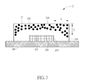
- FIG. 7 is a schematic view illustrating a package 2 ′ according to another embodiment of the disclosure.
- the molding compound 24 of the package 2 ′ only comprises one type of phosphor particles 248 , wherein a concentration per unit volume of the phosphor particles 248 increases gradually in a direction away from the main light emitting surface 206 of the light emitting unit 202 , as shown in FIG. 7 .
- the disclosure may selectively dope at least one type of phosphor particles in the molding compound 24 according to practical applications.
- FIG. 7 and FIG. 6 are represented by the same numerals, so the repeated explanation will not be depicted herein again.
- FIG. 8 is a schematic view illustrating a light emitting module 20 and a mold 22 ′ according to another embodiment of the disclosure
- FIG. 9 is a schematic view illustrating a package 2 ′′ according to another embodiment of the disclosure.
- the package method shown in FIG. 2 can use the mold 22 ′ shown in FIG. 8 to manufacture the package 2 ′′ shown in FIG. 9 .
- the main difference between the mold 22 ′ and the aforementioned mold 22 is that the mold 22 ′ only has one single recess 220 , as shown in FIG. 8 .
- the disclosure may use the single recess 220 of the mold 22 ′ to package a plurality of light emitting units 202 at the same time.
- the disclosure can increase the number of packages per unit volume. It should be noted that the same elements in FIGS. 8-9 and FIGS. 3-6 are represented by the same numerals, so the repeated explanation will not be depicted herein again.
- the disclosure fills the recess of the mold with the molding compound first and then places the substrate of the light emitting module on the mold reversely, so that the light emitting unit is immersed into the recess and the molding compound directly encapsulates the light emitting unit. Afterward, the disclosure heats and presses the substrate and the mold, so as to solidify the molding compound and finish the package. Then, the mold is removed from the light emitting module and the light emitting module is cut, so as to obtain a plurality of packages of the disclosure.
- the disclosure may dope at least two types of phosphor particles in the molding compound.
- the concentration per unit volume of the phosphor particles with shorter emission wavelength is larger than the concentration per unit volume of the phosphor particles with longer emission wavelength at a position away from the main light emitting surface of the light emitting unit, and the concentration per unit volume of the phosphor particles with shorter emission wavelength is smaller than the concentration per unit volume of the phosphor particles with longer emission wavelength at a position close to the main light emitting surface of the light emitting unit.
- the disclosure dopes at least two types of phosphor particles in the molding compound and the deposition rates of different phosphor particles are different from each other, different phosphor particles will be delaminated in the molding compound without additional process. Accordingly, the disclosure can save manufacture time effectively and needs not to use a shielding plate to form the molding compound, such that the quantity of phosphor particles in the molding compound can be reduced.
Landscapes
- Led Device Packages (AREA)
Abstract
Description
Claims (13)
Priority Applications (1)
| Application Number | Priority Date | Filing Date | Title |
|---|---|---|---|
| US15/627,430 US10090445B2 (en) | 2014-04-30 | 2017-06-19 | Package method and package |
Applications Claiming Priority (5)
| Application Number | Priority Date | Filing Date | Title |
|---|---|---|---|
| TW103115611A | 2014-04-30 | ||
| TW103115611A TWI528601B (en) | 2014-04-30 | 2014-04-30 | Packaging method and package structure |
| TW103115611 | 2014-04-30 | ||
| US14/690,480 US9685596B2 (en) | 2014-04-30 | 2015-04-20 | Package method and package |
| US15/627,430 US10090445B2 (en) | 2014-04-30 | 2017-06-19 | Package method and package |
Related Parent Applications (1)
| Application Number | Title | Priority Date | Filing Date |
|---|---|---|---|
| US14/690,480 Division US9685596B2 (en) | 2014-04-30 | 2015-04-20 | Package method and package |
Publications (2)
| Publication Number | Publication Date |
|---|---|
| US20170288100A1 US20170288100A1 (en) | 2017-10-05 |
| US10090445B2 true US10090445B2 (en) | 2018-10-02 |
Family
ID=54355849
Family Applications (2)
| Application Number | Title | Priority Date | Filing Date |
|---|---|---|---|
| US14/690,480 Expired - Fee Related US9685596B2 (en) | 2014-04-30 | 2015-04-20 | Package method and package |
| US15/627,430 Active US10090445B2 (en) | 2014-04-30 | 2017-06-19 | Package method and package |
Family Applications Before (1)
| Application Number | Title | Priority Date | Filing Date |
|---|---|---|---|
| US14/690,480 Expired - Fee Related US9685596B2 (en) | 2014-04-30 | 2015-04-20 | Package method and package |
Country Status (4)
| Country | Link |
|---|---|
| US (2) | US9685596B2 (en) |
| JP (1) | JP2015213170A (en) |
| CN (1) | CN105023992A (en) |
| TW (1) | TWI528601B (en) |
Families Citing this family (12)
| Publication number | Priority date | Publication date | Assignee | Title |
|---|---|---|---|---|
| TW201628218A (en) * | 2015-01-26 | 2016-08-01 | 艾笛森光電股份有限公司 | Phosphor sheet and light-emitting device with phosphor sheet |
| EP3098861B1 (en) | 2015-05-29 | 2020-05-06 | Nichia Corporation | Light emitting device, and method of manufacturing a light emitting device |
| TWI712187B (en) * | 2015-09-11 | 2020-12-01 | 晶元光電股份有限公司 | Light-emitting device and manufacturing method thereof |
| JP6790478B2 (en) * | 2016-06-14 | 2020-11-25 | 日亜化学工業株式会社 | Manufacturing method of light emitting device |
| US10886437B2 (en) | 2016-11-03 | 2021-01-05 | Lumileds Llc | Devices and structures bonded by inorganic coating |
| JP7011143B2 (en) * | 2016-11-30 | 2022-01-26 | 日亜化学工業株式会社 | Manufacturing method of light emitting device |
| CN107195757A (en) * | 2017-07-06 | 2017-09-22 | 庞绮琪 | A kind of LED encapsulation structure |
| CN107331751A (en) * | 2017-07-06 | 2017-11-07 | 庞绮琪 | The encapsulating structure of LED service lifes can be extended |
| CN111029451A (en) * | 2018-10-09 | 2020-04-17 | 合肥彩虹蓝光科技有限公司 | A kind of LED packaging method |
| KR102919988B1 (en) * | 2020-03-17 | 2026-01-29 | 엘지이노텍 주식회사 | Lighting module and lighting device having thereof |
| DE102021118451A1 (en) * | 2021-07-16 | 2023-01-19 | OSRAM Opto Semiconductors Gesellschaft mit beschränkter Haftung | METHOD OF MANUFACTURING AN OPTOELECTRONIC DEVICE AND OPTOELECTRONIC DEVICE |
| CN117577746B (en) * | 2023-11-21 | 2025-06-20 | 中山市光圣半导体科技有限公司 | Manufacturing method of LED light emitting device and LED light emitting device |
Citations (7)
| Publication number | Priority date | Publication date | Assignee | Title |
|---|---|---|---|---|
| US20060226759A1 (en) * | 2005-03-06 | 2006-10-12 | Sharp Kabushiki Kaisha | Light emitting device and fabricating method thereof |
| CN1874019A (en) | 2005-05-30 | 2006-12-06 | 夏普株式会社 | Light emitting device and manufacturing method thereof |
| US20070090379A1 (en) * | 2005-10-21 | 2007-04-26 | Goon Wool K | Light emitting device with adjustable reflector cup |
| US20090057690A1 (en) * | 2007-01-22 | 2009-03-05 | Cree, Inc. | Wafer level phosphor coating technique for warm light emitting diodes |
| CN1937270B (en) | 2005-09-22 | 2010-08-25 | 三洋电机株式会社 | light emitting device |
| CN102569277A (en) | 2010-12-28 | 2012-07-11 | 株式会社东芝 | LED package and manufacturing method thereof |
| US8659043B1 (en) * | 2013-02-19 | 2014-02-25 | Cooledge Lighting Inc. | Engineered-phosphor LED packages and related methods |
Family Cites Families (7)
| Publication number | Priority date | Publication date | Assignee | Title |
|---|---|---|---|---|
| US20050211991A1 (en) | 2004-03-26 | 2005-09-29 | Kyocera Corporation | Light-emitting apparatus and illuminating apparatus |
| TWI250668B (en) | 2004-09-27 | 2006-03-01 | Advanced Optoelectronic Tech | Light apparatus emitting light with multiple wavelengths via nanometer fluorescent material, light device and manufacturing method thereof |
| JP2009019163A (en) * | 2007-07-13 | 2009-01-29 | Sharp Corp | Phosphor particle assembly for light emitting device, light emitting device, and backlight device for liquid crystal display |
| US20100181582A1 (en) * | 2009-01-22 | 2010-07-22 | Intematix Corporation | Light emitting devices with phosphor wavelength conversion and methods of manufacture thereof |
| CN102248633A (en) * | 2011-05-10 | 2011-11-23 | 惠州速乐科技有限公司 | Molding and packaging technology of LED lamp bead and special die thereof |
| JP5711076B2 (en) | 2011-08-10 | 2015-04-30 | 日東電工株式会社 | Epoxy resin composition for optical semiconductor device and optical semiconductor device using the same |
| TWM475702U (en) | 2013-12-11 | 2014-04-01 | Genesis Photonics Inc | Light emitting diode package structure |
-
2014
- 2014-04-30 TW TW103115611A patent/TWI528601B/en active
-
2015
- 2015-04-14 CN CN201510175258.XA patent/CN105023992A/en active Pending
- 2015-04-20 US US14/690,480 patent/US9685596B2/en not_active Expired - Fee Related
- 2015-04-28 JP JP2015091826A patent/JP2015213170A/en active Pending
-
2017
- 2017-06-19 US US15/627,430 patent/US10090445B2/en active Active
Patent Citations (7)
| Publication number | Priority date | Publication date | Assignee | Title |
|---|---|---|---|---|
| US20060226759A1 (en) * | 2005-03-06 | 2006-10-12 | Sharp Kabushiki Kaisha | Light emitting device and fabricating method thereof |
| CN1874019A (en) | 2005-05-30 | 2006-12-06 | 夏普株式会社 | Light emitting device and manufacturing method thereof |
| CN1937270B (en) | 2005-09-22 | 2010-08-25 | 三洋电机株式会社 | light emitting device |
| US20070090379A1 (en) * | 2005-10-21 | 2007-04-26 | Goon Wool K | Light emitting device with adjustable reflector cup |
| US20090057690A1 (en) * | 2007-01-22 | 2009-03-05 | Cree, Inc. | Wafer level phosphor coating technique for warm light emitting diodes |
| CN102569277A (en) | 2010-12-28 | 2012-07-11 | 株式会社东芝 | LED package and manufacturing method thereof |
| US8659043B1 (en) * | 2013-02-19 | 2014-02-25 | Cooledge Lighting Inc. | Engineered-phosphor LED packages and related methods |
Non-Patent Citations (1)
| Title |
|---|
| Corresponding Chinese office action dated May 25, 2018. |
Also Published As
| Publication number | Publication date |
|---|---|
| US9685596B2 (en) | 2017-06-20 |
| TW201541667A (en) | 2015-11-01 |
| CN105023992A (en) | 2015-11-04 |
| US20150318453A1 (en) | 2015-11-05 |
| JP2015213170A (en) | 2015-11-26 |
| TWI528601B (en) | 2016-04-01 |
| US20170288100A1 (en) | 2017-10-05 |
Similar Documents
| Publication | Publication Date | Title |
|---|---|---|
| US10090445B2 (en) | Package method and package | |
| US10153404B2 (en) | LED with high thermal conductivity particles in phosphor conversion layer | |
| US8809083B2 (en) | Method of manufacturing light emitting diode | |
| CN106876534B (en) | A kind of packaging method of flip chip level LED light source | |
| US20160163932A1 (en) | Method of producing an optoelectronic component | |
| KR20110040694A (en) | Light emitting diodes and manufacturing method thereof | |
| US20120104435A1 (en) | Refractive index tuning of wafer level package leds | |
| CN103367599A (en) | Manufacturing method of light emitting diode packaging structure | |
| US20130175554A1 (en) | Led package substrate and method of manufacturing led package | |
| US20140217437A1 (en) | Light emitting apparatus and manufacturing method thereof | |
| US20130285096A1 (en) | Light emitting diode package and method for manufacturing the same | |
| US8896018B2 (en) | Vacuum tray and method of manufacturing light emitting device using the same | |
| CN103378263A (en) | Method for manufacturing light emitting diode encapsulating structure | |
| JP2015012299A (en) | Light-emitting device and method for manufacturing the same | |
| CN104934516A (en) | LED package having transparent heat insulation adhesive layer | |
| JP5816479B2 (en) | A method for manufacturing a semiconductor light emitting device. | |
| US20130065332A1 (en) | Method for manufacturing led with an encapsulant having a flat top face | |
| CN107452851A (en) | Light emitting diode packaging assembly and multiple color temperature lighting device | |
| CN207052621U (en) | Light emitting diode packaging assembly and multiple color temperature lighting device | |
| KR20130021129A (en) | Apparatus for manufacturing light emitting diode and manufacturing method using the same | |
| TW201901989A (en) | Light-emitting diode package component and method of fabricating the same, and multiple color temperature illumination device with LED package component including a wavelength conversion layer and a flip-chip LED die that has a light-emitting body and two electrode | |
| CN104425673A (en) | Method for manufacturing light emitting diode | |
| KR101436456B1 (en) | Method of Manufacturing LED Device Using EHD Pump | |
| CN103426977B (en) | LED encapsulation method | |
| WO2017025013A1 (en) | Led encapsulation substrate |
Legal Events
| Date | Code | Title | Description |
|---|---|---|---|
| AS | Assignment |
Owner name: GENESIS PHOTONICS INC., TAIWAN Free format text: ASSIGNMENT OF ASSIGNORS INTEREST;ASSIGNORS:HUNG, CHIN-HUA;LEE, HAO-CHUNG;LIN, YU-FENG;REEL/FRAME:042775/0293 Effective date: 20150331 |
|
| STCF | Information on status: patent grant |
Free format text: PATENTED CASE |
|
| MAFP | Maintenance fee payment |
Free format text: PAYMENT OF MAINTENANCE FEE, 4TH YEAR, LARGE ENTITY (ORIGINAL EVENT CODE: M1551); ENTITY STATUS OF PATENT OWNER: LARGE ENTITY Year of fee payment: 4 |
|
| AS | Assignment |
Owner name: NICHIA CORPORATION, JAPAN Free format text: ASSIGNMENT OF ASSIGNORS INTEREST;ASSIGNOR:GENESIS PHOTONICS INC.;REEL/FRAME:066044/0807 Effective date: 20231123 Owner name: GENESIS PHOTONICS INC., TAIWAN Free format text: ADDRESS CHANGE REGISTRATION FORM;ASSIGNOR:GENESIS PHOTONICS INC.;REEL/FRAME:066044/0133 Effective date: 20221201 Owner name: NICHIA CORPORATION, JAPAN Free format text: ASSIGNMENT OF ASSIGNOR'S INTEREST;ASSIGNOR:GENESIS PHOTONICS INC.;REEL/FRAME:066044/0807 Effective date: 20231123 |