US10090298B2 - Integrated packaging structure - Google Patents
Integrated packaging structure Download PDFInfo
- Publication number
- US10090298B2 US10090298B2 US15/447,800 US201715447800A US10090298B2 US 10090298 B2 US10090298 B2 US 10090298B2 US 201715447800 A US201715447800 A US 201715447800A US 10090298 B2 US10090298 B2 US 10090298B2
- Authority
- US
- United States
- Prior art keywords
- source
- gate
- region
- connection element
- electrode pad
- Prior art date
- Legal status (The legal status is an assumption and is not a legal conclusion. Google has not performed a legal analysis and makes no representation as to the accuracy of the status listed.)
- Active
Links
- 238000004806 packaging method and process Methods 0.000 title claims abstract description 38
- 239000004065 semiconductor Substances 0.000 claims description 12
- 230000005669 field effect Effects 0.000 claims description 4
- 239000002184 metal Substances 0.000 claims description 3
- 239000000758 substrate Substances 0.000 description 5
- 238000002955 isolation Methods 0.000 description 4
- 230000008901 benefit Effects 0.000 description 2
- 239000004593 Epoxy Substances 0.000 description 1
- 230000002146 bilateral effect Effects 0.000 description 1
- 238000011161 development Methods 0.000 description 1
- 238000000034 method Methods 0.000 description 1
- 238000012827 research and development Methods 0.000 description 1
- 230000003068 static effect Effects 0.000 description 1
Images


Classifications
-
- H—ELECTRICITY
- H01—ELECTRIC ELEMENTS
- H01L—SEMICONDUCTOR DEVICES NOT COVERED BY CLASS H10
- H01L27/00—Devices consisting of a plurality of semiconductor or other solid-state components formed in or on a common substrate
- H01L27/02—Devices consisting of a plurality of semiconductor or other solid-state components formed in or on a common substrate including semiconductor components specially adapted for rectifying, oscillating, amplifying or switching and having at least one potential-jump barrier or surface barrier; including integrated passive circuit elements with at least one potential-jump barrier or surface barrier
- H01L27/04—Devices consisting of a plurality of semiconductor or other solid-state components formed in or on a common substrate including semiconductor components specially adapted for rectifying, oscillating, amplifying or switching and having at least one potential-jump barrier or surface barrier; including integrated passive circuit elements with at least one potential-jump barrier or surface barrier the substrate being a semiconductor body
- H01L27/08—Devices consisting of a plurality of semiconductor or other solid-state components formed in or on a common substrate including semiconductor components specially adapted for rectifying, oscillating, amplifying or switching and having at least one potential-jump barrier or surface barrier; including integrated passive circuit elements with at least one potential-jump barrier or surface barrier the substrate being a semiconductor body including only semiconductor components of a single kind
- H01L27/085—Devices consisting of a plurality of semiconductor or other solid-state components formed in or on a common substrate including semiconductor components specially adapted for rectifying, oscillating, amplifying or switching and having at least one potential-jump barrier or surface barrier; including integrated passive circuit elements with at least one potential-jump barrier or surface barrier the substrate being a semiconductor body including only semiconductor components of a single kind including field-effect components only
- H01L27/088—Devices consisting of a plurality of semiconductor or other solid-state components formed in or on a common substrate including semiconductor components specially adapted for rectifying, oscillating, amplifying or switching and having at least one potential-jump barrier or surface barrier; including integrated passive circuit elements with at least one potential-jump barrier or surface barrier the substrate being a semiconductor body including only semiconductor components of a single kind including field-effect components only the components being field-effect transistors with insulated gate
-
- H—ELECTRICITY
- H01—ELECTRIC ELEMENTS
- H01L—SEMICONDUCTOR DEVICES NOT COVERED BY CLASS H10
- H01L23/00—Details of semiconductor or other solid state devices
- H01L23/48—Arrangements for conducting electric current to or from the solid state body in operation, e.g. leads, terminal arrangements ; Selection of materials therefor
- H01L23/488—Arrangements for conducting electric current to or from the solid state body in operation, e.g. leads, terminal arrangements ; Selection of materials therefor consisting of soldered or bonded constructions
- H01L23/495—Lead-frames or other flat leads
- H01L23/49517—Additional leads
- H01L23/4952—Additional leads the additional leads being a bump or a wire
-
- H—ELECTRICITY
- H01—ELECTRIC ELEMENTS
- H01L—SEMICONDUCTOR DEVICES NOT COVERED BY CLASS H10
- H01L23/00—Details of semiconductor or other solid state devices
- H01L23/48—Arrangements for conducting electric current to or from the solid state body in operation, e.g. leads, terminal arrangements ; Selection of materials therefor
- H01L23/488—Arrangements for conducting electric current to or from the solid state body in operation, e.g. leads, terminal arrangements ; Selection of materials therefor consisting of soldered or bonded constructions
- H01L23/495—Lead-frames or other flat leads
- H01L23/49503—Lead-frames or other flat leads characterised by the die pad
-
- H—ELECTRICITY
- H01—ELECTRIC ELEMENTS
- H01L—SEMICONDUCTOR DEVICES NOT COVERED BY CLASS H10
- H01L23/00—Details of semiconductor or other solid state devices
- H01L23/48—Arrangements for conducting electric current to or from the solid state body in operation, e.g. leads, terminal arrangements ; Selection of materials therefor
- H01L23/488—Arrangements for conducting electric current to or from the solid state body in operation, e.g. leads, terminal arrangements ; Selection of materials therefor consisting of soldered or bonded constructions
- H01L23/495—Lead-frames or other flat leads
- H01L23/49517—Additional leads
- H01L23/49524—Additional leads the additional leads being a tape carrier or flat leads
-
- H—ELECTRICITY
- H01—ELECTRIC ELEMENTS
- H01L—SEMICONDUCTOR DEVICES NOT COVERED BY CLASS H10
- H01L23/00—Details of semiconductor or other solid state devices
- H01L23/48—Arrangements for conducting electric current to or from the solid state body in operation, e.g. leads, terminal arrangements ; Selection of materials therefor
- H01L23/488—Arrangements for conducting electric current to or from the solid state body in operation, e.g. leads, terminal arrangements ; Selection of materials therefor consisting of soldered or bonded constructions
- H01L23/495—Lead-frames or other flat leads
- H01L23/49541—Geometry of the lead-frame
- H01L23/49562—Geometry of the lead-frame for devices being provided for in H01L29/00
-
- H—ELECTRICITY
- H01—ELECTRIC ELEMENTS
- H01L—SEMICONDUCTOR DEVICES NOT COVERED BY CLASS H10
- H01L23/00—Details of semiconductor or other solid state devices
- H01L23/48—Arrangements for conducting electric current to or from the solid state body in operation, e.g. leads, terminal arrangements ; Selection of materials therefor
- H01L23/488—Arrangements for conducting electric current to or from the solid state body in operation, e.g. leads, terminal arrangements ; Selection of materials therefor consisting of soldered or bonded constructions
- H01L23/495—Lead-frames or other flat leads
- H01L23/49575—Assemblies of semiconductor devices on lead frames
-
- H—ELECTRICITY
- H01—ELECTRIC ELEMENTS
- H01L—SEMICONDUCTOR DEVICES NOT COVERED BY CLASS H10
- H01L23/00—Details of semiconductor or other solid state devices
- H01L23/48—Arrangements for conducting electric current to or from the solid state body in operation, e.g. leads, terminal arrangements ; Selection of materials therefor
- H01L23/488—Arrangements for conducting electric current to or from the solid state body in operation, e.g. leads, terminal arrangements ; Selection of materials therefor consisting of soldered or bonded constructions
- H01L23/495—Lead-frames or other flat leads
- H01L23/49579—Lead-frames or other flat leads characterised by the materials of the lead frames or layers thereon
- H01L23/49586—Insulating layers on lead frames
-
- H—ELECTRICITY
- H01—ELECTRIC ELEMENTS
- H01L—SEMICONDUCTOR DEVICES NOT COVERED BY CLASS H10
- H01L29/00—Semiconductor devices adapted for rectifying, amplifying, oscillating or switching, or capacitors or resistors with at least one potential-jump barrier or surface barrier, e.g. PN junction depletion layer or carrier concentration layer; Details of semiconductor bodies or of electrodes thereof ; Multistep manufacturing processes therefor
- H01L29/02—Semiconductor bodies ; Multistep manufacturing processes therefor
- H01L29/06—Semiconductor bodies ; Multistep manufacturing processes therefor characterised by their shape; characterised by the shapes, relative sizes, or dispositions of the semiconductor regions ; characterised by the concentration or distribution of impurities within semiconductor regions
- H01L29/0603—Semiconductor bodies ; Multistep manufacturing processes therefor characterised by their shape; characterised by the shapes, relative sizes, or dispositions of the semiconductor regions ; characterised by the concentration or distribution of impurities within semiconductor regions characterised by particular constructional design considerations, e.g. for preventing surface leakage, for controlling electric field concentration or for internal isolations regions
- H01L29/0607—Semiconductor bodies ; Multistep manufacturing processes therefor characterised by their shape; characterised by the shapes, relative sizes, or dispositions of the semiconductor regions ; characterised by the concentration or distribution of impurities within semiconductor regions characterised by particular constructional design considerations, e.g. for preventing surface leakage, for controlling electric field concentration or for internal isolations regions for preventing surface leakage or controlling electric field concentration
- H01L29/0611—Semiconductor bodies ; Multistep manufacturing processes therefor characterised by their shape; characterised by the shapes, relative sizes, or dispositions of the semiconductor regions ; characterised by the concentration or distribution of impurities within semiconductor regions characterised by particular constructional design considerations, e.g. for preventing surface leakage, for controlling electric field concentration or for internal isolations regions for preventing surface leakage or controlling electric field concentration for increasing or controlling the breakdown voltage of reverse biased devices
- H01L29/0615—Semiconductor bodies ; Multistep manufacturing processes therefor characterised by their shape; characterised by the shapes, relative sizes, or dispositions of the semiconductor regions ; characterised by the concentration or distribution of impurities within semiconductor regions characterised by particular constructional design considerations, e.g. for preventing surface leakage, for controlling electric field concentration or for internal isolations regions for preventing surface leakage or controlling electric field concentration for increasing or controlling the breakdown voltage of reverse biased devices by the doping profile or the shape or the arrangement of the PN junction, or with supplementary regions, e.g. junction termination extension [JTE]
- H01L29/063—Reduced surface field [RESURF] pn-junction structures
- H01L29/0634—Multiple reduced surface field (multi-RESURF) structures, e.g. double RESURF, charge compensation, cool, superjunction (SJ), 3D-RESURF, composite buffer (CB) structures
-
- H—ELECTRICITY
- H01—ELECTRIC ELEMENTS
- H01L—SEMICONDUCTOR DEVICES NOT COVERED BY CLASS H10
- H01L29/00—Semiconductor devices adapted for rectifying, amplifying, oscillating or switching, or capacitors or resistors with at least one potential-jump barrier or surface barrier, e.g. PN junction depletion layer or carrier concentration layer; Details of semiconductor bodies or of electrodes thereof ; Multistep manufacturing processes therefor
- H01L29/40—Electrodes ; Multistep manufacturing processes therefor
- H01L29/41—Electrodes ; Multistep manufacturing processes therefor characterised by their shape, relative sizes or dispositions
- H01L29/417—Electrodes ; Multistep manufacturing processes therefor characterised by their shape, relative sizes or dispositions carrying the current to be rectified, amplified or switched
- H01L29/41725—Source or drain electrodes for field effect devices
-
- H—ELECTRICITY
- H01—ELECTRIC ELEMENTS
- H01L—SEMICONDUCTOR DEVICES NOT COVERED BY CLASS H10
- H01L2224/00—Indexing scheme for arrangements for connecting or disconnecting semiconductor or solid-state bodies and methods related thereto as covered by H01L24/00
- H01L2224/01—Means for bonding being attached to, or being formed on, the surface to be connected, e.g. chip-to-package, die-attach, "first-level" interconnects; Manufacturing methods related thereto
- H01L2224/02—Bonding areas; Manufacturing methods related thereto
- H01L2224/04—Structure, shape, material or disposition of the bonding areas prior to the connecting process
- H01L2224/06—Structure, shape, material or disposition of the bonding areas prior to the connecting process of a plurality of bonding areas
- H01L2224/0601—Structure
- H01L2224/0603—Bonding areas having different sizes, e.g. different heights or widths
-
- H—ELECTRICITY
- H01—ELECTRIC ELEMENTS
- H01L—SEMICONDUCTOR DEVICES NOT COVERED BY CLASS H10
- H01L2224/00—Indexing scheme for arrangements for connecting or disconnecting semiconductor or solid-state bodies and methods related thereto as covered by H01L24/00
- H01L2224/01—Means for bonding being attached to, or being formed on, the surface to be connected, e.g. chip-to-package, die-attach, "first-level" interconnects; Manufacturing methods related thereto
- H01L2224/26—Layer connectors, e.g. plate connectors, solder or adhesive layers; Manufacturing methods related thereto
- H01L2224/31—Structure, shape, material or disposition of the layer connectors after the connecting process
- H01L2224/32—Structure, shape, material or disposition of the layer connectors after the connecting process of an individual layer connector
- H01L2224/321—Disposition
- H01L2224/32151—Disposition the layer connector connecting between a semiconductor or solid-state body and an item not being a semiconductor or solid-state body, e.g. chip-to-substrate, chip-to-passive
- H01L2224/32221—Disposition the layer connector connecting between a semiconductor or solid-state body and an item not being a semiconductor or solid-state body, e.g. chip-to-substrate, chip-to-passive the body and the item being stacked
- H01L2224/32245—Disposition the layer connector connecting between a semiconductor or solid-state body and an item not being a semiconductor or solid-state body, e.g. chip-to-substrate, chip-to-passive the body and the item being stacked the item being metallic
-
- H—ELECTRICITY
- H01—ELECTRIC ELEMENTS
- H01L—SEMICONDUCTOR DEVICES NOT COVERED BY CLASS H10
- H01L2224/00—Indexing scheme for arrangements for connecting or disconnecting semiconductor or solid-state bodies and methods related thereto as covered by H01L24/00
- H01L2224/01—Means for bonding being attached to, or being formed on, the surface to be connected, e.g. chip-to-package, die-attach, "first-level" interconnects; Manufacturing methods related thereto
- H01L2224/34—Strap connectors, e.g. copper straps for grounding power devices; Manufacturing methods related thereto
- H01L2224/39—Structure, shape, material or disposition of the strap connectors after the connecting process
- H01L2224/40—Structure, shape, material or disposition of the strap connectors after the connecting process of an individual strap connector
- H01L2224/401—Disposition
- H01L2224/40151—Connecting between a semiconductor or solid-state body and an item not being a semiconductor or solid-state body, e.g. chip-to-substrate, chip-to-passive
- H01L2224/40221—Connecting between a semiconductor or solid-state body and an item not being a semiconductor or solid-state body, e.g. chip-to-substrate, chip-to-passive the body and the item being stacked
- H01L2224/40245—Connecting between a semiconductor or solid-state body and an item not being a semiconductor or solid-state body, e.g. chip-to-substrate, chip-to-passive the body and the item being stacked the item being metallic
-
- H—ELECTRICITY
- H01—ELECTRIC ELEMENTS
- H01L—SEMICONDUCTOR DEVICES NOT COVERED BY CLASS H10
- H01L2224/00—Indexing scheme for arrangements for connecting or disconnecting semiconductor or solid-state bodies and methods related thereto as covered by H01L24/00
- H01L2224/01—Means for bonding being attached to, or being formed on, the surface to be connected, e.g. chip-to-package, die-attach, "first-level" interconnects; Manufacturing methods related thereto
- H01L2224/42—Wire connectors; Manufacturing methods related thereto
- H01L2224/47—Structure, shape, material or disposition of the wire connectors after the connecting process
- H01L2224/48—Structure, shape, material or disposition of the wire connectors after the connecting process of an individual wire connector
- H01L2224/481—Disposition
- H01L2224/48151—Connecting between a semiconductor or solid-state body and an item not being a semiconductor or solid-state body, e.g. chip-to-substrate, chip-to-passive
- H01L2224/48221—Connecting between a semiconductor or solid-state body and an item not being a semiconductor or solid-state body, e.g. chip-to-substrate, chip-to-passive the body and the item being stacked
- H01L2224/48245—Connecting between a semiconductor or solid-state body and an item not being a semiconductor or solid-state body, e.g. chip-to-substrate, chip-to-passive the body and the item being stacked the item being metallic
- H01L2224/48247—Connecting between a semiconductor or solid-state body and an item not being a semiconductor or solid-state body, e.g. chip-to-substrate, chip-to-passive the body and the item being stacked the item being metallic connecting the wire to a bond pad of the item
-
- H—ELECTRICITY
- H01—ELECTRIC ELEMENTS
- H01L—SEMICONDUCTOR DEVICES NOT COVERED BY CLASS H10
- H01L2224/00—Indexing scheme for arrangements for connecting or disconnecting semiconductor or solid-state bodies and methods related thereto as covered by H01L24/00
- H01L2224/73—Means for bonding being of different types provided for in two or more of groups H01L2224/10, H01L2224/18, H01L2224/26, H01L2224/34, H01L2224/42, H01L2224/50, H01L2224/63, H01L2224/71
- H01L2224/732—Location after the connecting process
- H01L2224/73201—Location after the connecting process on the same surface
- H01L2224/73221—Strap and wire connectors
-
- H—ELECTRICITY
- H01—ELECTRIC ELEMENTS
- H01L—SEMICONDUCTOR DEVICES NOT COVERED BY CLASS H10
- H01L23/00—Details of semiconductor or other solid state devices
- H01L23/28—Encapsulations, e.g. encapsulating layers, coatings, e.g. for protection
- H01L23/31—Encapsulations, e.g. encapsulating layers, coatings, e.g. for protection characterised by the arrangement or shape
- H01L23/3107—Encapsulations, e.g. encapsulating layers, coatings, e.g. for protection characterised by the arrangement or shape the device being completely enclosed
-
- H—ELECTRICITY
- H01—ELECTRIC ELEMENTS
- H01L—SEMICONDUCTOR DEVICES NOT COVERED BY CLASS H10
- H01L25/00—Assemblies consisting of a plurality of individual semiconductor or other solid state devices ; Multistep manufacturing processes thereof
- H01L25/03—Assemblies consisting of a plurality of individual semiconductor or other solid state devices ; Multistep manufacturing processes thereof all the devices being of a type provided for in the same subgroup of groups H01L27/00 - H01L33/00, or in a single subclass of H10K, H10N, e.g. assemblies of rectifier diodes
- H01L25/04—Assemblies consisting of a plurality of individual semiconductor or other solid state devices ; Multistep manufacturing processes thereof all the devices being of a type provided for in the same subgroup of groups H01L27/00 - H01L33/00, or in a single subclass of H10K, H10N, e.g. assemblies of rectifier diodes the devices not having separate containers
- H01L25/07—Assemblies consisting of a plurality of individual semiconductor or other solid state devices ; Multistep manufacturing processes thereof all the devices being of a type provided for in the same subgroup of groups H01L27/00 - H01L33/00, or in a single subclass of H10K, H10N, e.g. assemblies of rectifier diodes the devices not having separate containers the devices being of a type provided for in group H01L29/00
- H01L25/072—Assemblies consisting of a plurality of individual semiconductor or other solid state devices ; Multistep manufacturing processes thereof all the devices being of a type provided for in the same subgroup of groups H01L27/00 - H01L33/00, or in a single subclass of H10K, H10N, e.g. assemblies of rectifier diodes the devices not having separate containers the devices being of a type provided for in group H01L29/00 the devices being arranged next to each other
-
- H—ELECTRICITY
- H01—ELECTRIC ELEMENTS
- H01L—SEMICONDUCTOR DEVICES NOT COVERED BY CLASS H10
- H01L2924/00—Indexing scheme for arrangements or methods for connecting or disconnecting semiconductor or solid-state bodies as covered by H01L24/00
- H01L2924/15—Details of package parts other than the semiconductor or other solid state devices to be connected
- H01L2924/181—Encapsulation
Definitions
- the present invention is related to an integrated packaging structure, and more particularly is related to an integrated packaging structure with two dies integrated into one packaging structure.
- MOSFET metal-oxide-semiconductor field-effect transistor
- an integrated packaging structure is provided in the present invention, which packages two dies in the same package so as to shorten the conductive path and reduce the size of the packaging structure as well as the packaging substrate.
- the IC unit includes a main body, a first metal-oxide-semiconductor field-effect transistor (MOSFET) die, a second MOSFET die, at least one first source connection element, at least one second source connection element, at least one first gate connection element, and at least one second gate connection element.
- the main body has a first source region, a second source region, a first gate region, a second gate region, a first setting region, and a second setting region, which are separated from each other.
- the first MOSFET die is located on the first setting region, has a first upper layer, and comprises at least one first source electrode pad and at least one first gate electrode pad.
- the at least one first source electrode pad is exposed through the first upper layer.
- the at least one first gate electrode pad is spaced apart from the at least one first source electrode pad and is also exposed through the first upper layer.
- the second MOSFET die is located on the second setting region, has a second upper layer, and comprises at least one second source electrode pad and at least one second gate electrode pad.
- the at least one second source electrode pad is exposed through the second upper layer.
- the at least one second gate electrode pad is spaced apart from the at least one second source electrode pad, and is also exposed through the second upper layer.
- the at least one first source connection element is connected to the at least one first source electrode pad and the first source region.
- the at least one second source connection element is connected to the at least one second source electrode pad and the second source region.
- the at least one first gate connection element is connected to the at least one first gate electrode pad and the first gate region.
- the at least one second gate connection element is connected to the at least one second gate electrode pad and the second gate region.
- the packaging body at least partially covers the IC unit. Wherein, the first MOSFET die and the second MOSFET die are super junction MOSFET dies.
- the first source region includes at least one first source pin
- the second source region includes at least one second source pin
- the first gate region includes at least one first gate pin
- the second gate region includes at least one second gate pin
- the at least one first gate pin, the at least one first source pin, the at least one second source pin, and the at least one second gate pin are arranged along a direction in a serial.
- the at least first source connection element and the at least one second source connection element are one-piece metal clips, and the at least first gate connection element and the at least one second gate connection element are at least one conductive wire.
- the first source region is adjacent to the second source region, and a distance, which is greater than 1.805 mm, is left between the first setting region and the second setting region.
- the at least first source connection element and the at least one second source connection element are at least one conductive wire.
- the gate electrode pads may be arranged at the corners of the MOSFET die so as to increase IC layout flexibility in practice.
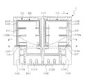
- FIG. 1 is a top view of an integrated packaging structure provided in accordance with a preferred embodiment of the present invention.
- FIG. 2 is a cross-section view of the integrated packaging structure provided in accordance with the preferred embodiment of the present invention.
- FIG. 1 is a top view of an integrated packaging structure provided in accordance with a preferred embodiment of the present invention
- FIG. 2 is a cross-section view of the integrated packaging structure provided in accordance with the preferred embodiment of the present invention.
- the integrated packaging structure 1 provided in accordance with a preferred embodiment of the present invention comprises an integrated circuit (IC) unit 11 and a packaging body 12 .
- the IC unit 11 includes a main body 111 , a first metal-oxide-semiconductor field-effect transistor (MOSFET) die 112 , a second MOSFET die 113 , at least one first source connection element 114 , at least one second source connection element 115 , at least one first gate connection element 116 , and at least one second gate connection element 117 .
- MOSFET metal-oxide-semiconductor field-effect transistor
- the main body 111 such as a lead frame, has a first source region 1111 , a second source region 1112 , a first gate region 1113 , a second gate region 1114 , a first setting region 1115 , a second setting region 1116 , which are separated from each other, and the main body also has an isolation region 1117 .
- the first source region 1111 includes at least one first source pin 11111 (three pins are shown in the figure and one of them is labelled), the second source region 1112 is adjacent to the first source region 1111 , and the second source region 1112 includes at least one second source pin 11121 (three pins are shown in the figure and one of them is labelled).
- the first gate region 1113 includes at least one first gate pin 11131 (only one is shown in the figure), the second gate region 1114 includes at least one second gate pin 11141 (only one is shown in the figure).
- the at least one first gate pin 11131 , the at least one first source pin 11111 , the at least one second source pin 11112 , and the at least one second gate pin 11141 are arranged along a direction L in a serial so as to have the source pins and the gate pins showing the arrangement of bilateral symmetry. It would facilitate the research and development personnel to design the layout of the wires connected to the source electrode pad (the detail would be described in the following paragraphs).
- the first setting region 1115 and the second setting region 1116 are opposite to each other through the isolation region 1117 . That is, the first setting region 1115 and the second setting region 1116 are separated from each other.
- the isolation region 1117 may be filled with epoxy.
- a relatively large distance W is left in the isolation region 1117 , i.e. between the first setting region 1115 and the second setting region 1116 .
- the distance W may be greater than 1.805 mm to enhance the withstanding voltage (up to 600V for example), however, the present invention is not so restricted.
- the withstanding voltage can be enhanced to 1000V. That is, the withstanding voltage can be changed by adjusting the distance W (in general, the value of the withstanding voltage is proportional to the distance W), and thus the present invention is not restricted to the aforementioned examples.
- the first MOSFET die 112 is located on the first setting region 1115 , has a first upper layer 1121 and a first lower layer 1122 , and includes at least one first source electrode pad 1123 (three pads are shown in the figure, and one of them is labelled), at least one first gate electrode pad (two electrode pads 1124 and 1124 a are shown), at least one drain electrode pad 1125 , and at least one first semiconductor structure 1126 .
- the at least one first source electrode pad 1123 is exposed through the first upper layer 1121 .
- the first gate electrode pads 1124 and 1124 a are spaced apart from the at least one first source electrode pad 1123 and is also exposed through the first upper layer 1121 .
- the first gate electrode pads 1124 and 1124 a are arranged at the corresponding corners (the lower-left corner and the lower-right corner in the figure), however, the present invention is not so restricted.
- the at least one first drain electrode pad 1125 is exposed through the first lower layer 1122 .
- the first semiconductor structure 1126 is located between the first source electrode pad 1123 and the first drain electrode pad 1125 .
- the first semiconductor structure 1126 is composed of the conventional circuit architecture, and thus is not repeated here.
- the second MOSFET die 113 is located on the second setting region 1116 , has a second upper layer 1131 and a second lower layer 1132 , and includes at least one second source electrode pad 1133 (three electrode pads are shown in the figure, and one of them is labelled), at least one second gate electrode pad (two electrode pads 1134 and 1134 a are shown), at least one second drain electrode pad 1135 , and a second semiconductor structure 1136 .
- the at least one second source electrode pad 1133 is exposed through the second upper layer 1131 .
- the second gate electrode pads 1134 and 1134 a are spaced apart from the at least one second source electrode pad 1133 and is exposed through the second upper layer 1131 .
- the second gate electrode pads 1134 and 1134 a are arranged at the corresponding corners (the lower-left corner and the lower-right corner in the figure), however, the present invention is not so restricted.
- the at least one second drain electrode pad 1135 is exposed through the second lower layer 1132 .
- the second semiconductor structure 1136 is located between the second source electrode pad 1133 and the second drain electrode pad 1135 .
- the second semiconductor structure 1136 is composed of the conventional circuit architecture, and thus is not repeated here.
- the first MOSFET die 112 and the second MOSFET die 113 of the present embodiment are super-junction MOSFET dies featuring the super junction technology, however, the present invention is not so restricted.
- the at least one first source connection element 114 (several connection elements are shown in the figure and only one of them is labelled) is connected to the at least one first source electrode pad 1123 and the at least one first source pin 11111 in the first source region 1111 .
- the at least one second source connection element 115 (several connection elements are shown in the figure and only one of them is labelled) is connected to the at least one second source electrode pad 1133 and the at least one second source pin 11112 in the second source region 1112 .
- the at least first source connection element 114 and the at least one second source connection element 115 are one-piece metal clips, however, the present invention is not so restricted.
- the conductive wires fabricated by using the wire-bonding process can also be used in the present invention.
- the at least one first gate connection element 116 is connected to the first gate electrode pad 1124 and the first gate pin 11131 in the first gate region 1113 , and the at least one first gate connection element 116 is a conductive wire.
- the at least one second gate connection element 117 is connected to the second gate electrode pad 1134 and the second gate pin 11141 in the second gate region 1114 , and the at least one second gate connection element 117 is also a conductive wire, however, the present invention is not so restricted.
- the packaging body 12 at least partially covers the IC unit 11 . The usage of the packaging body 12 is common to those skilled in the art and thus is not repeated here.
- the two MOSFET dies are packaged into one single packaging body, conductive loss can be effectively reduced to generate a stable output and the size of the packaging substrate can also be effectively reduced.
- the gate electrode pads may be arranged at the corresponding corners of the MOSFET dies so as to increase IC layout flexibility in practice.
Abstract
Description
Claims (6)
Applications Claiming Priority (3)
| Application Number | Priority Date | Filing Date | Title |
|---|---|---|---|
| TW106201068U | 2017-01-20 | ||
| TW106201068U TWM544108U (en) | 2017-01-20 | 2017-01-20 | Integrated packaging structure |
| TW106201068 | 2017-01-20 |
Publications (2)
| Publication Number | Publication Date |
|---|---|
| US20180211953A1 US20180211953A1 (en) | 2018-07-26 |
| US10090298B2 true US10090298B2 (en) | 2018-10-02 |
Family
ID=59688569
Family Applications (1)
| Application Number | Title | Priority Date | Filing Date |
|---|---|---|---|
| US15/447,800 Active US10090298B2 (en) | 2017-01-20 | 2017-03-02 | Integrated packaging structure |
Country Status (2)
| Country | Link |
|---|---|
| US (1) | US10090298B2 (en) |
| TW (1) | TWM544108U (en) |
Families Citing this family (1)
| Publication number | Priority date | Publication date | Assignee | Title |
|---|---|---|---|---|
| WO2023279794A1 (en) * | 2021-07-06 | 2023-01-12 | 南京芯干线科技有限公司 | Switch power device |
Citations (2)
| Publication number | Priority date | Publication date | Assignee | Title |
|---|---|---|---|---|
| US20080054422A1 (en) * | 2006-08-30 | 2008-03-06 | Nobuya Koike | Semiconductor device |
| US20080173991A1 (en) * | 2007-01-24 | 2008-07-24 | Erwin Victor Cruz | Pre-molded clip structure |
-
2017
- 2017-01-20 TW TW106201068U patent/TWM544108U/en not_active IP Right Cessation
- 2017-03-02 US US15/447,800 patent/US10090298B2/en active Active
Patent Citations (2)
| Publication number | Priority date | Publication date | Assignee | Title |
|---|---|---|---|---|
| US20080054422A1 (en) * | 2006-08-30 | 2008-03-06 | Nobuya Koike | Semiconductor device |
| US20080173991A1 (en) * | 2007-01-24 | 2008-07-24 | Erwin Victor Cruz | Pre-molded clip structure |
Also Published As
| Publication number | Publication date |
|---|---|
| TWM544108U (en) | 2017-06-21 |
| US20180211953A1 (en) | 2018-07-26 |
Similar Documents
| Publication | Publication Date | Title |
|---|---|---|
| US8294256B2 (en) | Chip package structure and method of making the same | |
| US10242148B2 (en) | Integrated circuit and routing design of the same | |
| TWI593031B (en) | Semiconductor integrated circuit device | |
| CN105529317B (en) | Embedded packaging system | |
| CN103824853B (en) | Integrated circuit module applied to switch type regulator | |
| CN102376669A (en) | Semiconductor device with a plurality of transistors | |
| US10056355B2 (en) | Common-source packaging structure | |
| TWI621221B (en) | Semiconductor package and lead frame | |
| US10090298B2 (en) | Integrated packaging structure | |
| CN105529306B (en) | Semiconductor component | |
| US11605578B2 (en) | Chip package assembly and method for manufacturing the same | |
| CN105489578A (en) | Laminated chip packaging structure | |
| JP2010258366A (en) | Semiconductor device | |
| US20140138762A1 (en) | Semiconductor device | |
| TWM538236U (en) | Common source type packaging structure | |
| US8729632B2 (en) | Semiconductor structure with low resistance of substrate and low power consumption | |
| TWM606602U (en) | High-power integrated circuit chip packaging device | |
| US9997429B2 (en) | Trench-type heat sink structure applicable to semiconductor device | |
| TW201310594A (en) | Packaging structure | |
| US9847312B2 (en) | Package structure | |
| US20170271234A1 (en) | Bonding wire-type heat sink structure for semiconductor devices | |
| CN203800034U (en) | Semiconductor device packaging lead frame | |
| TW201824465A (en) | Package structures | |
| CN209515654U (en) | SOT dual chip lead frame structure and SOT dual chip lead frame assembly | |
| CN108122900A (en) | The encapsulating structure of DC-DC conversion circuit |
Legal Events
| Date | Code | Title | Description |
|---|---|---|---|
| AS | Assignment |
Owner name: TAIWAN SEMICONDUCTOR CO., LTD., TAIWAN Free format text: ASSIGNMENT OF ASSIGNORS INTEREST;ASSIGNORS:CHEN, CHIEN-CHUNG;MAO, SEN;LIN, HSIN-LIANG;REEL/FRAME:041453/0372 Effective date: 20161230 |
|
| STCF | Information on status: patent grant |
Free format text: PATENTED CASE |
|
| FEPP | Fee payment procedure |
Free format text: ENTITY STATUS SET TO UNDISCOUNTED (ORIGINAL EVENT CODE: BIG.); ENTITY STATUS OF PATENT OWNER: LARGE ENTITY |
|
| MAFP | Maintenance fee payment |
Free format text: PAYMENT OF MAINTENANCE FEE, 4TH YEAR, LARGE ENTITY (ORIGINAL EVENT CODE: M1551); ENTITY STATUS OF PATENT OWNER: LARGE ENTITY Year of fee payment: 4 |