US10082621B2 - Display apparatus - Google Patents
Display apparatus Download PDFInfo
- Publication number
- US10082621B2 US10082621B2 US15/228,356 US201615228356A US10082621B2 US 10082621 B2 US10082621 B2 US 10082621B2 US 201615228356 A US201615228356 A US 201615228356A US 10082621 B2 US10082621 B2 US 10082621B2
- Authority
- US
- United States
- Prior art keywords
- fixing part
- guide plate
- fixing
- light guide
- light
- Prior art date
- Legal status (The legal status is an assumption and is not a legal conclusion. Google has not performed a legal analysis and makes no representation as to the accuracy of the status listed.)
- Active, expires
Links
Images


Classifications
-
- G—PHYSICS
- G02—OPTICS
- G02B—OPTICAL ELEMENTS, SYSTEMS OR APPARATUS
- G02B6/00—Light guides; Structural details of arrangements comprising light guides and other optical elements, e.g. couplings
- G02B6/0001—Light guides; Structural details of arrangements comprising light guides and other optical elements, e.g. couplings specially adapted for lighting devices or systems
- G02B6/0011—Light guides; Structural details of arrangements comprising light guides and other optical elements, e.g. couplings specially adapted for lighting devices or systems the light guides being planar or of plate-like form
- G02B6/0081—Mechanical or electrical aspects of the light guide and light source in the lighting device peculiar to the adaptation to planar light guides, e.g. concerning packaging
- G02B6/0086—Positioning aspects
- G02B6/0091—Positioning aspects of the light source relative to the light guide
-
- G—PHYSICS
- G02—OPTICS
- G02B—OPTICAL ELEMENTS, SYSTEMS OR APPARATUS
- G02B6/00—Light guides; Structural details of arrangements comprising light guides and other optical elements, e.g. couplings
- G02B6/0001—Light guides; Structural details of arrangements comprising light guides and other optical elements, e.g. couplings specially adapted for lighting devices or systems
- G02B6/0011—Light guides; Structural details of arrangements comprising light guides and other optical elements, e.g. couplings specially adapted for lighting devices or systems the light guides being planar or of plate-like form
- G02B6/0013—Means for improving the coupling-in of light from the light source into the light guide
- G02B6/0015—Means for improving the coupling-in of light from the light source into the light guide provided on the surface of the light guide or in the bulk of it
- G02B6/002—Means for improving the coupling-in of light from the light source into the light guide provided on the surface of the light guide or in the bulk of it by shaping at least a portion of the light guide, e.g. with collimating, focussing or diverging surfaces
-
- G—PHYSICS
- G02—OPTICS
- G02B—OPTICAL ELEMENTS, SYSTEMS OR APPARATUS
- G02B6/00—Light guides; Structural details of arrangements comprising light guides and other optical elements, e.g. couplings
- G02B6/0001—Light guides; Structural details of arrangements comprising light guides and other optical elements, e.g. couplings specially adapted for lighting devices or systems
- G02B6/0011—Light guides; Structural details of arrangements comprising light guides and other optical elements, e.g. couplings specially adapted for lighting devices or systems the light guides being planar or of plate-like form
- G02B6/0013—Means for improving the coupling-in of light from the light source into the light guide
- G02B6/0023—Means for improving the coupling-in of light from the light source into the light guide provided by one optical element, or plurality thereof, placed between the light guide and the light source, or around the light source
- G02B6/0031—Reflecting element, sheet or layer
-
- G—PHYSICS
- G02—OPTICS
- G02F—OPTICAL DEVICES OR ARRANGEMENTS FOR THE CONTROL OF LIGHT BY MODIFICATION OF THE OPTICAL PROPERTIES OF THE MEDIA OF THE ELEMENTS INVOLVED THEREIN; NON-LINEAR OPTICS; FREQUENCY-CHANGING OF LIGHT; OPTICAL LOGIC ELEMENTS; OPTICAL ANALOGUE/DIGITAL CONVERTERS
- G02F1/00—Devices or arrangements for the control of the intensity, colour, phase, polarisation or direction of light arriving from an independent light source, e.g. switching, gating or modulating; Non-linear optics
- G02F1/01—Devices or arrangements for the control of the intensity, colour, phase, polarisation or direction of light arriving from an independent light source, e.g. switching, gating or modulating; Non-linear optics for the control of the intensity, phase, polarisation or colour
- G02F1/13—Devices or arrangements for the control of the intensity, colour, phase, polarisation or direction of light arriving from an independent light source, e.g. switching, gating or modulating; Non-linear optics for the control of the intensity, phase, polarisation or colour based on liquid crystals, e.g. single liquid crystal display cells
- G02F1/133—Constructional arrangements; Operation of liquid crystal cells; Circuit arrangements
- G02F1/136—Liquid crystal cells structurally associated with a semi-conducting layer or substrate, e.g. cells forming part of an integrated circuit
- G02F1/1362—Active matrix addressed cells
Definitions
- Exemplary embodiments of the invention herein relate to a display apparatus, and more particularly, to a display apparatus which fixes a light source to a light guide plate to improve light efficiency.
- a display apparatus in general, includes a display panel for displaying an image and a backlight unit for providing light to the display panel.
- the display panel includes a first substrate on which a plurality of pixels is disposed, a second substrate facing the first substrate, and an image display layer disposed between the first and second substrates.
- the image display layer is driven by the pixels, and an optical transmittance received from the backlight unit is adjusted by the image display layer to display the image.
- the image display layer may be a liquid crystal layer, an electrowetting layer, or electrophoresis layer, for example.
- the backlight unit may be classified into an edge type backlight unit disposed on a side surface of the display apparatus to generate light and a direct type backlight unit disposed under the display panel to generate light.
- the edge type backlight unit includes a light source for generating light and a light guide plate for guiding the light received from the light source upward.
- the light source is spaced apart from the light guide plate by a predetermined distance.
- a portion of a light generated from a light source may not be provided to a light guide plate due to a gap between the light source and the light guide plate. Thus, a light incident efficiency may be deteriorated.
- the invention provides a display apparatus that fixes a light source to a light guide plate to improve light efficiency.
- Exemplary embodiments of the invention provide display apparatuses including a display panel which displays an image using light, a plurality of light source units arranged in a first direction to generate the light, a light guide plate which receives the light to guide the light to the display panel, a first fixing member which fixes a predetermined area of an upper portion of each of the light source units to a first area of one side surface of the light guide plate, which is adjacent to a top surface of the light guide plate in a second direction crossing the first direction, and a second fixing member which fixes a predetermined area of a lower portion of each of the light source units to a second area of the one side surface of the light guide plate, which is adjacent to a bottom surface of the light guide plate in the second direction, where each of the first and second fixing members includes a light reflection material.
- a predetermined area of a front surface of each of the light source units, which faces the one side surface of the light guide plate, may contact one side surface of the light guide plate between the first area and the second area.
- the one side surface of the light guide plate may include a first side surface that is parallel to a third direction perpendicular to a plane parallel to the first and second directions and is parallel to the first direction, a second side surface connected to an upper end of the first side surface, the second side surface including an inclined surface extending at a first acute angle with respect to the second direction in a plane defined by an upward direction of the third direction and a right direction of the second direction, and a third side surface connected to a lower end of the first side surface, the third side surface including an inclined surface extending at a second acute angle with respect to the second direction in a plane defined by a downward direction of the third direction and the right direction of the second direction, where the first fixing member may be connected to the predetermined area of the upper portion of each of the light source unit and the second side surface, the second fixing member may be connected to the predetermined area of the lower portion of each of the light source units and the third side surface, and the right direction of the second direction may be directed from the first side surface to an opposite
- first acute angle and the second acute angle may be the same with each other.
- the first fixing member may include a first fixing part which extends in the first direction, and a second fixing part which extends in the first direction, the second fixing part connected to a predetermined area of a bottom surface of the first fixing part, which is adjacent to one side surface of the first fixing part in the second direction, where the one side surface of the first fixing part may include a first inclined surface extending at the first acute angle with respect to the second direction in a plane defined by the downward direction of the third direction and a left direction of the second direction, and the second fixing part may have a right-angled triangular shape when viewed in the first direction, a second inclined surface defined as an oblique side of the second fixing part may extend at the first acute angle and be disposed on the same plane as the first inclined surface, and a first side of the first side and a second side of the second fixing part, which are connected to define a right angle, may be disposed on a predetermined area of the bottom surface of the first fixing part, which is adjacent to the first inclined surface.
- the second fixing member may include a third fixing part which extends in the first direction, and a fourth fixing part which extends in the first direction, the fourth fixing part connected to a predetermined area of a top surface of the second fixing part, which is adjacent to one side surface of the second fixing part in the second direction, where the one side surface of the third fixing part may include a third inclined surface extending at the second acute angle with respect to the second direction in a plane defined in the upward direction of the third direction and the left direction of the second direction, and the fourth fixing part may have a right-angled triangular shape when viewed in the first direction, a fourth inclined surface defined as an oblique side of the fourth fixing part may extend at the second acute angle and be disposed on the same plane as the third inclined surface, and a third side of the third side and a fourth side of the fourth fixing part, which are connected to define the right angle, may be disposed on a predetermined area of the top surface of the third fixing part, which is adjacent to the third inclined surface.
- each of the first and third fixing parts may include a light reflection material
- each of the second and fourth fixing parts may include a light transmitting material
- each of the second and fourth fixing parts may have the same refractive index as that of the light guide plate.
- first and third inclined surfaces may be disposed on the second side surface, and the third and fourth inclined surfaces may be disposed on a lower portion of the third side surface.
- the display apparatuses may further include an adhesion member which connects the first inclined surface to the second side surface and the third inclined surface to the third side surface.
- the light source unit may include a bottom part facing the first side surface, the bottom part parallel to the first and third directions, a first sidewall part connected to an upper end of the bottom part to extend in the second direction toward the one side surface of the light guide plate, a second sidewall part connected to a lower end of the bottom part to extend in the second direction toward the one side surface of the light guide plate, the second sidewall part facing the first sidewall part, a light emitting diode disposed on the bottom part to face the first side surface, and a molding part disposed on the bottom part to cover the light emitting diode, the molding part disposed between the first and second sidewall parts.
- a front surface of the first sidewall part toward the one side surface of the light guide plate may contact a predetermined area of the second side of the second fixing part, which is adjacent to the bottom surface of the first fixing part, and a front surface of the second sidewall part toward the one side surface of the light guide plate may contact a predetermined area of the fourth side of the fourth fixing part, which is adjacent to the top surface of the third fixing part.
- the bottom surface of the first fixing part, on which the first side of the second fixing part is not disposed may be disposed on a predetermined area of an outer surface of the first sidewall part, which is adjacent to the front surface of the first sidewall part
- the top surface of the third fixing part, on which the third side of the fourth fixing part is not disposed may be disposed on a lower portion of a predetermined area of an outer surface of the second sidewall part, which is adjacent to the front surface of the second sidewall part
- the outer surface of the first sidewall part may be a surface opposite to an inner surface of the first sidewall part on which the molding part is disposed
- the outer surface of the second sidewall part may be a surface opposite to an inner surface of the second sidewall part on which the molding part is disposed.
- the display apparatuses may further include an adhesion member which connects the bottom surface of the first fixing part, on which the first side of the second fixing part is not disposed, to a predetermined area of the outer surface of the first sidewall part, which is adjacent to the front surface of the first sidewall part, and which connects the top surface of the third fixing part, on which the third side of the fourth fixing part is not disposed, to a predetermined area of the outer surface of the second sidewall part, which is adjacent to the front surface of the second sidewall part.
- a front surface of the molding part toward the one side surface of the light guide plate may contact the first side surface, a predetermined area of the second side of the second fixing part, which is adjacent to the upper end of the first side surface, and a predetermined area of the fourth side of the fourth fixing part, which is adjacent to the lower end of the first side surface.
- FIG. 1 is an exploded perspective view of an exemplary embodiment of a display apparatus according to the invention
- FIG. 2 is a view illustrating a side surface of a predetermined portion on a side of a light guide plate of FIG. 1 ;
- FIG. 3 is an equivalent circuit view of one pixel of pixels disposed on a display panel of FIG. 1 ;
- FIG. 4 is an enlarged view of first and second fixing members of FIG. 1 ;
- FIG. 5 is a side view of the first and second fixing members when the first and second fixing members of FIG. 4 are viewed in a first direction;
- FIG. 6 is a cross-sectional view illustrating a state in which a light source unit of FIG. 1 is connected to the light guide plate through the first and second fixing members;
- FIGS. 7 to 11 are views illustrating components of first and second fixing members of a display apparatus according to various exemplary embodiments of the invention.
- first,” “second,” “third” etc. may be used herein to describe various elements, components, regions, layers and/or sections, these elements, components, regions, layers and/or sections should not be limited by these terms. These terms are only used to distinguish one element, component, region, layer or section from another element, component, region, layer or section. Thus, “a first element,” “component,” “region,” “layer” or “section” discussed below could be termed a second element, component, region, layer or section without departing from the teachings herein.
- first and second are used herein to describe various elements, these elements should not be limited by these terms. These terms are only used to distinguish one component from another component. Accordingly, a first element, a first component, or a first section that will be described below may be a second element, a second component, or a second section within the technical idea of the invention.
- “About” or “approximately” as used herein is inclusive of the stated value and means within an acceptable range of deviation for the particular value as determined by one of ordinary skill in the art, considering the measurement in question and the error associated with measurement of the particular quantity (i.e., the limitations of the measurement system). In an exemplary embodiment, “about” can mean within one or more standard deviations, or within ⁇ 30%, 20%, 10%, 5% of the stated value.
- Exemplary embodiments are described herein with reference to cross section illustrations that are schematic illustrations of idealized embodiments. As such, variations from the shapes of the illustrations as a result, for example, of manufacturing techniques and/or tolerances, are to be expected. Thus, embodiments described herein should not be construed as limited to the particular shapes of regions as illustrated herein but are to include deviations in shapes that result, for example, from manufacturing. In an exemplary embodiment, a region illustrated or described as flat may, typically, have rough and/or nonlinear features. Moreover, sharp angles that are illustrated may be rounded. Thus, the regions illustrated in the DRAWINGS are schematic in nature and their shapes are not intended to illustrate the precise shape of a region and are not intended to limit the scope of the claims.
- FIG. 1 is an exploded perspective view of a display apparatus according to an exemplary embodiment of the invention.
- FIG. 2 is a view illustrating a side surface of a predetermined portion on a side of a light guide plate of FIG. 1 .
- FIG. 3 is an equivalent circuit view of one pixel of pixels disposed on a display panel of FIG. 1 .
- a display apparatus 100 includes a display panel 110 for displaying an image using light and a backlight unit BLU generating light to provide the generated light to the display panel 110 .
- the display panel 110 has a long side in a first direction DR 1 and a short side in a second direction DR 2 crossing the first direction DR 1 .
- the backlight unit BLU may be disposed at a rear side of the display panel 110 to provide the light to the display panel 110 .
- the display panel 110 includes a plurality of pixels for displaying an image using light.
- Each of the pixels may display one of primary colors.
- the primary colors may include red, green, and blue colors, for example. However, the invention is not limited thereto.
- the primary colors may further include various other colors such as a white color, a yellow color, cyan, and magenta.
- the display panel 110 may be a liquid crystal display panel including a liquid crystal layer, for example.
- the display panel 110 may include a first substrate 111 on which the plurality of pixels are disposed, a second substrate 112 facing the first substrate 111 , and a liquid crystal layer LC disposed between the first substrate 111 and the second substrate 112 , for example.
- the invention is not limited thereto.
- the display panel 110 may be an electrophoretic display panel including an electrophoretic layer or an electrowetting display panel including an electrowetting layer, for example.
- the backlight unit BLU may be an edge type backlight unit.
- the backlight unit BLU includes an optical sheet 120 , a light guide plate 130 , a light source LS, fixing member 10 and 20 , and a reflection sheet 140 .
- Each of the optical sheet 120 , the light guide plate 130 , and the reflection sheet 140 has a long side in the first direction DR 1 and a short side in a second direction DR 2 .
- the light source LS and the fixing members 10 and 20 extend in the first direction DR 1 .
- a third direction DR 3 may be defined as a direction perpendicular to a plane parallel to the first and second directions DR 1 and DR 2 . Also, each of the first, second, and third directions DR 1 , DR 2 , and DR 3 may be bidirectionally defined.
- the optical sheet 120 is disposed on an upper portion of the light guide plate 130
- the reflection sheet 140 is disposed on a lower portion of the light guide plate 130
- the display panel 110 is disposed on an upper portion of the optical sheet 120 .
- the light source LS is disposed adjacent to one side of the light guide plate 130 in the second direction DR 2 .
- the light source LS may be connected to one side of the light guide plate 130 by the fixing members 10 and 20 .
- Surfaces SS 1 , SS 2 , and SS 3 of the light guide plate 130 include a first side surface SS 1 parallel to a plane defined by the first and third directions DR 1 and DR 3 , a second side surface SS 2 connected to an upper end of the first side surface SS 1 and having an inclined surface, and a third side surfaces SS 3 connected to a lower end of the first side surface SS 1 and having an inclined surface.
- the second side surface SS 2 and the third side surface SS 3 may have shapes that are symmetrical to each other and defined as chamfers.
- the second side surface SS 2 of the light guide plate 130 may be defined as a first area that is adjacent to a top surface of the light guide plate 130
- the third side surface SS 3 of the light guide plate 130 may be defined as a second area that is adjacent to a bottom surface of the light guide plate 130 .
- the top surface of the light guide plate 139 may be disposed at a height greater than that of an upper end of the first side surface SS 1
- the bottom surface of the light guide plate 130 may be disposed at a height less than that of the first side surface SS 1 .
- Each of the top and bottom surfaces of the light guide plate 130 in the second direction DR 2 has a length less than a distance between the first side surface SS 1 of the light guide plate 130 and an opposite side surface of the light guide plate 130 , which is opposite to the first side surface SS 1 .
- the second side surface SS 2 may be defined as an inclined surface having a first acute angle ⁇ 1 with respect to the second direction DR 2 in a plane defined by an upward direction of the third direction DR 3 and a right direction of the second direction DR 2 .
- the right direction of the second direction DR 2 may be defined as a direction that is directed from the first side surface SS 1 of the light guide plate 130 toward the opposite side surface of the light guide plate 130 .
- the second side surface SS 2 extends at the first acute angle ⁇ 1 with respect to the second direction DR 2 to connect the upper end of the first side surface SS 1 to one side of the top surface of the light guide plate 130 .
- the third side surface SS 3 may be defined as an inclined surface having a second acute angle ⁇ 2 with respect to the second direction DR 2 in a plane defined by a downward direction of the third direction DR 3 and the right direction of the second direction DR 2 .
- the third side surface SS 3 extends at the second acute angle ⁇ 2 with respect to the second direction DR 2 to connect the lower end of the first side surface SS 1 to one side of the bottom surface of the light guide plate 130 .
- Each of the first and second acute angles ⁇ 1 and ⁇ 2 may be defined as an angle less than the right angle.
- the first acute angle ⁇ 1 may be defined as the same angle as that of the second acute angle ⁇ 2 , for example.
- the invention is not limited thereto, and thus, the first acute angle ⁇ 1 may be different from the second acute angle ⁇ 2 .
- the opposite side surface of the light guide plate 130 connects the other side of the top surface of the light guide plate 130 to the other side of the bottom surface of the light guide plate in the second direction DR 2 .
- the first side surface SS 1 of the light guide plate 130 may be defined as a light incident part, and the opposite side surface of the light guide plate may be defined as a light emission part.
- the light guide plate 130 may include glass. However, the invention is not limited thereto. In an exemplary embodiment, the light guide plate 130 may include a plastic material such as polymethyl methacrylate (“PMMA”).
- PMMA polymethyl methacrylate
- the light source LS includes a light source substrate SUB extending in the first direction DR 1 and a plurality of light source units LSU disposed (e.g., mounted) on the light source substrate SUB.
- the light source units LSU is disposed on an entire surface of the light source substrate SUB facing the first side surface SS 1 of the light guide plate 130 in the second direction DR 2 .
- the light source units LSU may be disposed at a predetermined interval in the first direction DR 1 . In an exemplary embodiment, the light source units LSU may be disposed at the same distance from each other, for example.
- the light source units LSU face the first side surface SS 1 of the light guide plate 130 .
- the fixing members 10 and 20 include a first fixing member 10 disposed on an upper portion of the light source LS and a second fixing member 20 disposed on a lower portion of the light source LS.
- the first fixing member 10 includes a light reflection material.
- the first fixing member 10 fixes a predetermined area of an upper portion of each of the light source units LSU to the second side surface SS 2 that is the first area of the side surfaces SS 1 , SS 2 , and SS 3 .
- the second fixing member 20 includes a light reflection material.
- the second fixing member 20 fixes a predetermined area of a lower portion of each of the light source units LSU to the second side surface SS 2 that is the second area of the side surfaces SS 1 , SS 2 , and SS 3 .
- the light source units LSU of the light source LS generate light to be used in the display panel 110 .
- the light generated in the light source units LSU is provided to the light incident part of the light guide plate 130 in the second direction DR 2 .
- the light guide plate 130 guides the light to the display panel 110 .
- the light guide plate 130 may change a traveling direction of the light provided from the light source units LSU so that the light travels in the upward direction in which the display panel 110 is disposed, for example.
- the reflection sheet 140 reflects the light emitted to a lower side of the light guide plate 130 so that the light is emitted upward.
- the optical sheet 120 includes a diffusion sheet (not shown) and a prism sheet (not shown) disposed on the diffusion sheet.
- the diffusion sheet may diffuse the light provided from the light guide plate 130 .
- the prism sheet may collect the light diffused by the diffusion sheet in the upward direction that is perpendicular to the plane.
- the light passing through the prism sheet may travels upward and be provided to the display panel 110 with uniform luminance distribution.
- the display panel 110 may display an image using the light provided thereto.
- the display panel 110 includes the first substrate 111 , the second substrate 112 facing the first substrate 111 , and the light crystal layer LC disposed between the first substrate 111 and the second substrate 112 .
- the pixel includes a transfer TR connected to a gate line GLi and a data line DLj, a liquid crystal capacitor Clc connected to the transistor TR, and a storage capacitor Cst parallelly connected to the liquid crystal capacitor Clc, where I and j are natural numbers.
- the storage capacitor Cst may be omitted.
- the gate line GLi extends in the first direction DR 1
- the data line DLj extends in the second direction DR 2 .
- the transistor TR may be disposed on the first substrate 111 .
- the transistor TR includes a gate electrode connected to the gate line GLi, a source electrode connected to the data line DLj, and a drain electrode connected to the liquid crystal capacitor Clc and the storage capacitor Cst.
- the liquid crystal capacitor Clc includes a pixel electrode PE disposed on the first substrate 111 , a common electrode CE disposed on the second substrate 112 , and the liquid crystal layer LC disposed between the pixel electrode PE and the common electrode CE.
- the liquid crystal layer LC may serve as a dielectric.
- the pixel electrode PE is connected to the drain electrode of the transistor TR. In an exemplary embodiment, the pixel electrode PE may be disposed between adjacent data lines DLj and DLj+1.
- the pixel electrode PE has a non-slit structure in FIG. 3 , the invention is not limited thereto.
- the pixel electrode PE may have a slit structure including a stem part having a cross shape and a plurality of branch parts radially extending from the stem part, for example.
- the common electrode CE may be disposed over an entire surface of the second substrate 112 .
- the invention is not limited thereto.
- the common electrode CE may be disposed on the first substrate 111 , for example.
- at least one of the pixel electrode PE and the common electrode CE may have a slit.
- the storage capacitor Cst may include the pixel electrode PE, a storage electrode (not shown) that is branched from a storage line (not shown), and an insulation layer disposed between the pixel electrode PE and the storage electrode.
- the storage line is disposed on the first substrate 111 . Also, the storage line may be simultaneously provided together with the gate line GLi on the same layer.
- the storage electrode may partially overlap the pixel electrode PE.
- the pixel may further include a color filter CF for representing one of red, green, and blue colors.
- the color filter CF may be disposed on the second substrate 112 as illustrated in FIG. 3 .
- the invention is not limited thereto.
- the color filter CF may be disposed on the first substrate 111 , for example.
- the transistor TR is turned on in response to s gate signal provided through the gate line GLi.
- a data voltage received through the data line DLj is provided to the pixel electrode PE of the liquid crystal capacitor Clc through the transistor TR that is turned on.
- a common voltage is applied to the common electrode CE.
- Electric fields are generated between the pixel electrode PE and the common electrode CE by a difference in voltage level between the data voltage and the common voltage.
- Liquid crystal molecules of the liquid crystal layer LC operate by the electric fields generated between the pixel electrode PE and the common electrode CE.
- Light transmittance may be adjusted by the liquid crystal molecules that operate by the electric field to display an image.
- a storage voltage having a uniform voltage level may be applied to the storage line.
- the common voltage may be applied to the storage line, for example.
- the storage capacitor Cst may supplement a voltage that is charged in the liquid crystal capacitor Clc.
- pixels of the display panel 110 may have the same configuration as that of the pixel of FIG. 3 .
- FIG. 4 is an enlarged view of the first and second fixing members of FIG. 1 .
- FIG. 5 is a side view of the first and second fixing members when the first and second fixing members of FIG. 4 are viewed in a first direction.
- each of the first and second fixing members 10 and 20 extends in the first direction DR 1 .
- the first and second fixing members 10 and 20 face each other in the third direction DR 3 .
- the first fixing member 10 includes a fixing part 11 extending in the first direction DR 1 and a second fixing part 12 extending in the first direction DR 1 and connected to a predetermined area of a bottom surface of the first fixing part 11 that is adjacent to one side surface of the first fixing part 11 in the second direction DR 2 .
- the first fixing part 11 has a long side in the first direction DR 1 and a short side in the second direction DR 2 .
- a top surface of the first fixing part 11 has a length in the second direction DR 2 greater than that of the bottom surface of the first fixing part 11 .
- One side surface of the first fixing part 11 may be defined as a first inclined surface SL 1 having a predetermined inclination.
- the opposite side surface of the first fixing part 11 which is a surface opposite to the one side surface of the first fixing part 11 , may be a surface parallel to a plane defined by the first direction DR 1 and the third direction DR 3 .
- the first inclined surface SL 1 of the first fixing part 11 extends at the first acute angle ⁇ 1 with respect to the second direction DR 2 in the plane defined by the downward direction of the third direction DR 3 and a left direction of the second direction DR 2 .
- the left direction of the second direction DR 2 may be defined as a direction that is opposite to the right direction of the second direction DR 2 .
- the first inclined surface SL 1 connects one side of the top surface of the first fixing part 11 to one side of the bottom surface of the first fixing part 11 .
- the second fixing part 12 is connected to a predetermined area of the bottom surface of the first fixing part 11 adjacent to the first inclined surface SL 1 of the first fixing part 11 in the second direction DR 2 .
- the second fixing part 12 has a right-angled triangular shape when viewed in the first direction DR 1 , for example.
- the side facing the right angle in the right-angled triangular shape may be defined as an oblique side.
- the oblique side of the second fixing part 12 which faces the right angle in the second fixing part 12 , may be defined as a second inclined surface SL 2 .
- the second inclined surface SL 2 of the second fixing part 12 extends at the first acute angle ⁇ 1 with respect to the second direction DR 2 in the plane defined by the downward direction of the third direction DR 3 and the left direction of the second direction DR 2 .
- the first inclined surface SL 1 of the first fixing part 11 and the second inclined surface SL 2 of the second fixing part 12 may be disposed on the same plane.
- Each of the first inclined surface SL 1 and the second inclined surface SL 2 may be an inclined surface having the same first acute angle ⁇ 1 as that of the second side surface SS 2 .
- a first side S 1 of first and second sides S 1 and S 2 of the second fixing part 12 which are connected to define a right angle, may be disposed on a predetermined area of the bottom surface of the first fixing part 11 , which is adjacent to the first inclined surface SL 1 of the first fixing part 11 .
- the second fixing part 12 may be connected to the first fixing part 11 using an adhesive.
- the first fixing part 11 may reflect light.
- the first fixing part 11 may include a light reflection material such as a white mold or a metal material.
- the second fixing part 12 may transmit light therethrough.
- the second fixing part 12 may include a light transmitting material such as silicon, acrylic resin, or polyimide (“PI”).
- the second fixing member 20 may be disposed under the first fixing member 10 , and the first and second fixing members 10 and 20 may face each other.
- the second fixing member 20 may have the same shape as that of the first fixing member 10 and include the same material as that of the first fixing member 10 . Also, the first and second fixing members 10 and 20 may be disposed symmetrical to each other.
- the second fixing member 20 includes a third fixing part 21 having the same shape as that of the first fixing part 11 and including the same material as that of the first fixing part 11 and a fourth fixing part 22 having the same shape as that of the second fixing part 12 and including the same material as that of the second fixing part 12 , for example.
- Each of the second and fourth fixing parts 12 and 22 may have the same refractive index as that of the light guide plate 130 .
- the third fixing part 21 may be disposed under the first fixing part 11 to face the first fixing part 11 .
- the first and third fixing parts 11 and 21 may be disposed symmetrical to each other.
- the fourth fixing part 22 may be disposed under the second fixing part 12 to face the second fixing part 12 .
- the second and fourth fixing parts 12 and 22 may be disposed symmetrical to each other.
- One side surface of the third fixing part 21 may be defined as a third inclined surface SL 3 having a predetermined inclination, and an oblique side of the fourth fixing part 22 having a triangular shape may be defined as a fourth inclined surface SL 4 .
- a third side S 3 of third and fourth sides S 3 and S 4 of the fourth fixing part 22 which are connected to define a right angle, may be disposed on a predetermined area of a top surface of the third fixing part 21 , which is adjacent to the third inclined surface SL 3 of the third fixing part 21 .
- Each of the third inclined surface SL 3 and the fourth inclined surface SL 4 extends at the second acute angle ⁇ 2 with respect to the second direction DR 2 in the plane defined by the upward direction of the third direction DR 3 and the left direction of the second direction DR 2 .
- the third inclined surface SL 3 and the fourth inclined surface SL 4 may be disposed on the same plane.
- Each of the third inclined surface SL 3 and the fourth inclined surface SL 4 may be an inclined surface having the same second acute angle ⁇ 2 as that of the third side surface SS 3 .
- FIG. 6 is a cross-sectional view illustrating a state in which the light source unit of FIG. 1 is connected to the light guide plate through the first and second fixing members.
- the light source substrate SUB is omitted. Also, one light source unit LSU, the first and second fixing members 10 and 20 , one side surface of the light guide plate 130 , and a cross-section of a predetermined area of the light guide plate 130 , which is adjacent to one side surface of the light guide plate 130 , are illustrated in FIG. 6 .
- the light source unit LSU includes a housing HO, a light emitting diode LED accommodated in the housing HO, and a molding part MO disposed on the housing HO to cover the light emitting diode LED.
- the housing HO includes a bottom part BT that is parallel to the first and third direction DR 1 and DR 3 , a first sidewall part SW 1 connected to an upper end of the bottom part BT to extend in the second direction DR 2 , and a second sidewall part SW 2 connected to a lower end of the bottom part BT to extend in the second direction DR 2 .
- the first sidewall part SW 1 and the second sidewall part SW 2 face each other.
- the bottom part BT faces the first side surface SS 1 of the light guide plate 130 , and the first and second sidewall parts SW 1 and SW 2 extend to one side surface of the light guide plate 130 .
- the light emitting diode LED and the molding part MO are accommodated in a space between the bottom part BT and the first and second sidewall parts SW 1 and SW 2 .
- the light emitting diode LED is disposed on the bottom part BT to face the first side surface SS 1 of the light guide plate 130 , for example.
- the molding part MO is disposed on the bottom part BT to cover the light emitting diode LED and also be disposed between the first and second sidewall parts SW 1 and SW 2 .
- Surfaces of the first and second sidewall parts SW 1 and SW 2 which face the side surfaces SS 1 , SS 2 , and SS 3 of the light guide plate 130 , and a surface of the molding part MO may be defined as front surfaces of the first and second sidewall parts SW 1 and SW 2 and a front surface of the molding part MO, respectively.
- a thickness of the light source unit LSU in the third direction DR 3 is less than that of the light guide plate 130 .
- a length of the front surface of the molding part MO in the third direction DR 3 is greater than that of the first side surface SS 1 of the light guide plate 130 .
- the first fixing member 10 adheres to or is connected to a predetermined area of an upper portion of the light source unit LSU and the second side surface SS 2 of the light guide plate 130 .
- the second fixing member adheres to or is connected to a predetermined area of a lower portion of the light source unit LSU.
- the light source unit LSU may be connected to one side of the light guide plate 130 .
- a bottom surface of the first fixing part 11 on which the first side S 1 of the second fixing part 12 is not disposed may be disposed on a predetermined area of an outer surface of the first sidewall part SW 1 , which is adjacent to the front surface of the first sidewall part SW 1 .
- the outer surface of the first sidewall part SW 1 may be defined as a surface that is opposite to an inner surface of the first sidewall part SW 1 on which the molding part MO is disposed.
- the bottom surface of the first fixing part 11 on which the first side S 1 of the second fixing part 12 is not disposed may adhere to or be connected to a predetermined area of the outer surface of the first sidewall part SW 1 , which is adjacent to the front surface of the first sidewall part SW 1 , using an adhesion member AH.
- the top surface of the third fixing part 21 on which the third side S 3 of the fourth fixing part 22 is not disposed may be disposed on a lower portion of a predetermined area of the outer surface of the second sidewall part SW 2 , which is adjacent to the front surface of the second sidewall part SW 2 .
- the outer surface of the second sidewall part SW 1 may be defined as a surface that is opposite to an inner surface of the second sidewall part SW 2 on which the molding part MO is disposed.
- the top surface of the third fixing part 21 on which the third side S 3 of the fourth fixing part 22 is not disposed may adhere to or be connected to a predetermined area of the outer surface of the second sidewall part SW 2 , which is adjacent to the front surface of the second sidewall part SW 2 , using the adhesion member AH.
- the top surfaces of the first fixing part 11 and the light guide plate 130 may be disposed at the same height.
- the bottom surfaces of the third fixing part 21 and the light guide plate 130 may be disposed at the same height.
- the first inclined surface SL 1 of the first fixing part 11 and the second inclined surface SL 2 of the second fixing part 12 may be disposed on the second side surface SS 2 of the light guide plate 130 .
- the first inclined surface SL 1 may adhere to or be connected to the second side surface SS 2 using the adhesion member AH.
- the third inclined surface SL 3 of the third fixing part 21 and the fourth inclined surface SL 4 of the fourth fixing part 22 may be disposed on a lower portion of the third side surface SS 3 of the light guide plate 130 .
- the third inclined surface SL 3 may adhere to or be connected to the third side surface SS 3 using the adhesion member AH.
- the front surface of the molding part MO and the front surfaces of the first and second sidewall parts SW 1 and SW 2 may be disposed on the first side surface SS 1 of the light guide plate 130 , the second side S 2 of the second fixing part 12 , and the fourth side S 4 of the fourth fixing part 22 by the first and second fixing members 10 and 20 .
- the front surface of the first sidewall part SW 1 may contact a predetermined area of the second side S 2 of the second fixing part 12 , which is adjacent to the bottom surface of the first fixing part 11 .
- the front surface of the second sidewall part SW 2 may contact a predetermined area of the fourth side S 4 of the fourth fixing part 22 , which is adjacent to the top surface of the third fixing part 21 .
- the front surface of the molding part MO and the front surfaces of the first and second sidewall parts SW 1 and SW 2 may be defined as a front surface of the light source unit LSU.
- a predetermined area of the front surface of the light source unit LSU may contact the first side surface SS 1 of the light guide plate 130 , which is disposed between the second side surface SS 2 and the third side surface SS 3 .
- the front surface of the molding part MO may contact the first side surface SS 1 of the light guide plate 130 , a predetermined area of the second side S 2 of the second fixing part 12 , which is adjacent to the upper end of the first side surface SS 1 , and a predetermined area of the fourth side S 4 of the fourth fixing part 22 , which is adjacent to the lower end of the first side surface SS 1 , for example.
- the light source unit LSU may be firmly fixed to one side of the light guide plate 130 by the above-described configurations. Also, the light source unit LSU may contact the first side surface SS 1 of the light guide plate 130 to provide a more amount of light to the light guide plate 130 . Light emitted between the first sidewall part SW 1 and the first side surface SS 1 and between the second sidewall part SW 2 and the first side surface SS 1 may be reflected by the first and second fixing parts 11 and 21 , which reflect light, and thus be reduced in light loss. As a result, light incident efficiency may be improved.
- the light source LS may be firmly fixed to the one side of the light guide plate 130 and also contact the one side surface of the light guide plate 130 to improve the light incident efficiency.
- FIGS. 7 to 11 are views illustrating components of first and second fixing members of a display apparatus according to another exemplary embodiment of the invention.
- the display apparatus may have the same configuration as that of the display apparatus 100 of FIG. 1 except for configurations of first and second fixing members 10 _ 1 and 20 _ 1 .
- first and second fixing members 10 _ 1 and 20 _ 1 differences between the first and second fixing members 10 and 20 of FIG. 6 and the first and second fixing members 10 _ 1 and 20 _ 1 of FIG. 7 will be mainly described for explaining the first and second fixing members 10 _ 1 and 20 _ 1 of FIG. 7 .
- the same components will be represented by the same reference numerals.
- the first fixing units 10 _ 1 are disposed on light source units LSU, and the second fixing units 20 _ 1 are disposed under the light source units LSU.
- the first fixing units 10 _ 1 respectively correspond to the light source units LSU
- the second fixing units 20 _ 1 respectively correspond to the light source units LSU. That is, the first fixing units 10 _ 1 may correspond to the light source units LSU in one-to-one correspondence, and the second fixing units 20 _ 1 may correspond to the light source units LSU in one-to-one correspondence.
- the first and second fixing units 10 _ 1 and 20 _ 1 may have the same width as that of the light source units LSU in a first direction DR 1 (refer to FIG. 4 ). Each of the first fixing units 10 _ 1 may be disposed to face the corresponding second fixing units 20 _ 1 in a third direction DR 3 .
- the first and second fixing units 10 _ 1 and 20 _ 1 may have the same cross-section as that of the first and second fixing units 10 and 20 of FIG. 6 .
- the structure in which the first and second fixing units 10 _ 1 and 20 _ 1 fix the light source units LSU to a light guide plate may be substantially the same as that in which the first and second fixing members 10 and 20 fix the light source units LSU to the light guide plate 130 .
- Each of the first fixing units 10 _ 1 may fix a predetermined area of an upper portion of the corresponding light source unit LSU of the light source units LSU to a second side surface SS 2 of one side surface of the light guide plate.
- Each of the second fixing units 20 _ 1 may fix a predetermined area of a lower portion of the corresponding light source unit LSU of the light source units LSU to a third side surface SS 3 of one side surface of the light guide plate.
- the light source LS may be firmly fixed to the light guide plate to improve light incident efficiency.
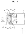
- FIGS. 8 to 11 are views illustrating components of first and second fixing members of a display apparatus according to another exemplary embodiment of the invention.
- the display apparatus may have the same configuration as that of the display apparatus 100 of FIG. 1 except for configurations of first and second fixing members 10 _ 2 and 20 _ 2 and a light source unit LSU_ 1 .
- first and second fixing members 10 and 20 and the light source unit LSU of FIG. 6 and the first and second fixing members 10 _ 2 and 20 _ 2 and the light source unit LSU_ 1 of FIG. 8 will be mainly described for explaining the first and second fixing members 10 _ 2 and 20 _ 2 and the light source unit LSU_ 1 of FIG. 8 .
- the same components will be represented by the same reference numerals.
- connection configurations between the first and second fixing members 10 _ 2 and 20 _ 2 , one light source unit LSU_ 1 , and the light guide plate 130 are illustrated in FIG. 8 .
- a thickness of the light source unit LSU_ 1 in the third direction DR 3 is less than that of the light source unit LSU.
- a length of the molding part MO_ 1 of the light source unit LSU_ 1 in the third direction DR 3 may be equal to that of the first side surface SS 1 of the light guide plate 130 by the above-described configurations.
- Other configurations of the light source unit LSU_ 1 are substantially the same as those of the light source unit LSU of FIG. 6 , and thus, descriptions thereof will be omitted.
- the first fixing member 10 _ 2 includes a first fixing part 11 _ 1 and a second fixing part 11 _ 2 protruding downward from one side of a bottom surface of the first fixing part 11 _ 1 , which is adjacent to the light guide plate 130 in the second direction DR 2 .
- the first and second fixing parts 11 _ 1 and 11 _ 2 extend in the first direction DR 1 , like the first and second fixing parts 11 and 12 of FIG. 4 .
- Each of the first and second fixing parts 11 _ 1 and 11 _ 2 may include a light reflection material.
- One side surface of the first fixing part 11 _ 1 may be defined as a fifth inclined surface SL 5 extending at a first acute angle ⁇ 1 (refer to FIG. 2 ), like the first inclined surface SL 1 .
- the second fixing part 11 _ 2 includes a first protrusion side surface PS 1 extending in the third direction DR 3 and a first protrusion oblique side PH 1 extending from the fifth inclined surface SL 5 at the first acute angle ⁇ 1 and connected to a lower end of the first protrusion side surface PS 1 .
- the second fixing member 20 _ 2 includes a third fixing part 21 _ 1 and a fourth fixing part 21 _ 2 protruding upward from one side of a top surface of the third fixing part 21 _ 1 , which is adjacent to the light guide plate 130 in the second direction DR 2 .
- the third and fourth fixing parts 21 _ 1 and 21 _ 2 extend in the first direction DR 1 , like the third and fourth fixing parts 21 and 22 of FIG. 4 .
- Each of the third and fourth fixing parts 21 _ 1 and 21 _ 2 may include a light reflection material.
- One side surface of the third fixing part 21 _ 1 may be defined as a sixth inclined surface SL 6 extending at a second acute angle ⁇ 2 (refer to FIG. 2 ), like the third inclined surface SL 3 .
- the fourth fixing part 21 _ 2 includes a second protrusion side surface PS 2 extending in the third direction DR 3 and a second protrusion oblique side PH 2 extending from the sixth inclined surface SL 6 at the second acute angle ⁇ 2 and connected to an upper end of the second protrusion side surface PS 2 .
- the fifth inclined surface SL 5 and the first protrusion oblique side PH 1 may be disposed on the second side surface SS 2 and then connected to the second side surface SS 2 using an adhesion member AH.
- the sixth inclined surface SL 6 and the second protrusion oblique side PH 2 may be disposed on a lower portion of the third side surface SS 3 of the light guide plate 130 and then connected to the third side surface SS 3 using the adhesion member AH.
- a front surface of the first sidewall part SW 1 _ 1 of the light source unit LSU_ 1 may contact the first protrusion side surface PS 1 of the second fixing part 11 _ 2 .
- a front surface of the second sidewall part SW 2 _ 1 of the light source unit LSU_ 1 may contact the second protrusion side surface PS 2 of the fourth fixing part 21 _ 2 .
- the bottom surface of the first fixing part 11 _ 1 may adhere to or be connected to a predetermined area of an upper portion of the light source unit LSU, and the top surface of the third fixing part 21 _ 1 may adhere to or be connected to a predetermined area of a lower portion of the light source unit LSU.
- the bottom surface of the first fixing part 11 _ 1 may be disposed on a predetermined area of an outer surface of the first sidewall part SW 1 _ 1 , which is adjacent to the front surface of the first sidewall part SW 1 _ 1 and then may adhere to or be connected to the predetermined area of the outer surface of the first sidewall part SW 1 _ 1 , which is adjacent to the front surface of the first sidewall part SW 1 _ 1 using the adhesion member AH.
- the top surface of the third fixing part 21 _ 1 may be disposed on a lower portion of a predetermined area of an outer surface of the second sidewall part SW 2 _ 1 , which is adjacent to the front surface of the second sidewall part SW 2 _ 1 and then may adhere to or be connected to the predetermined area of the outer surface of the second sidewall part SW 2 _ 1 , which is adjacent to the front surface of the second sidewall part SW 2 _ 1 using the adhesion member AH.
- a front surface of the molding part MO_ 1 may contact the first side surface SS 1 of the light guide plate 130 .
- the light source unit LSU_ 1 may be firmly fixed to one side of the light guide plate 130 by the first and second fixing members 10 _ 2 and 20 _ 2 . Also, the light source unit LSU_ 1 may contact the first side surface SS 1 of the light guide plate 130 to provide a more amount of light to the light guide plate 130 . As a result, light incident efficiency may be improved.
- FIG. 9 is a view illustrating components of first and second fixing members of the display apparatus according to another exemplary embodiment of the invention.
- the display apparatus may have the same configuration as that of the display apparatus 100 of FIG. 1 except for configurations of first and second fixing members 10 _ 3 and 20 _ 3 .
- first and second fixing members 10 _ 3 and 20 _ 3 differences between the first and second fixing members 10 and 20 of FIG. 6 and the first and second fixing members 10 _ 3 and 20 _ 3 of FIG. 9 will be mainly described for explaining the first and second fixing members 10 _ 3 and 10 _ 3 of FIG. 9 .
- connection configurations between the first and second fixing members 10 _ 3 and 20 _ 3 , one light source unit LSU, and the light guide plate 130 are illustrated in FIG. 9 .
- the first fixing member 10 _ 3 includes a first sub fixing part 11 _ 3 disposed on the first fixing part 11 .
- the first sub fixing part 11 _ 3 may be unitary with the first fixing part 11 .
- the first sub fixing part 11 _ 3 includes a first portion P 1 extending in the second direction DR 2 and disposed on a predetermined area of the top surface of the light guide plate 130 , which is adjacent to the second sidewall SS 2 of the light guide plate 130 .
- the first portion P 1 of the first sub fixing part 11 _ 3 may adhere to or be connected to a predetermined area of the top surface of the light guide plate 130 , which is adjacent to the second sidewall SS 2 of the light guide plate 130 using the adhesion member AH.
- Other configurations of the first fixing member 10 _ 3 may be substantially the same as those of the first fixing member 10 of FIG. 6 , and thus, descriptions thereof will be omitted.
- the second fixing member 20 _ 3 includes a second sub fixing part 21 _ 3 disposed on a lower portion of the third fixing part 21 .
- the second sub fixing part 21 _ 3 may be unitary with the third fixing part 21 .
- the second sub fixing part 21 _ 3 includes a second portion P 2 extending in the second direction DR 2 and disposed on a lower portion of a predetermined area of the bottom surface of the light guide plate 130 , which is adjacent to the third sidewall SS 3 of the light guide plate 130 .
- the second portion P 2 of the second sub fixing part 21 _ 3 may adhere to or be connected to a predetermined area of the bottom surface of the light guide plate 130 , which is adjacent to the third sidewall SS 3 of the light guide plate 130 using the adhesion member AH.
- Other configurations of the second fixing member 20 _ 3 may be substantially the same as those of the second fixing member 20 of FIG. 6 , and thus, descriptions thereof will be omitted.
- the light source unit LSU may be firmly fixed to one side of the light guide plate 130 by the first and second fixing members 10 _ 3 and 20 _ 3 . Thus, the light source unit LSU may contact the first side surface SS 1 of the light guide plate 130 , thereby improving light incident efficiency.
- FIGS. 10 and 11 are views illustrating components of first and second fixing members of the display apparatus according to various embodiments of the invention.
- the display apparatus may have the same configuration as that of the display apparatus 100 of FIG. 1 except for a structure in which the light source unit LSU is fixed to the light guide plate by one fixing member of the fixing members 10 and 20 .
- the same components will be represented by the same reference numerals.
- the fixing member 10 fixes a predetermined area of an upper portion of the light source unit LSU to the second side surface SS 2 of the side surfaces SS 1 , SS 2 , and SS 3 of the light guide plate 130 . Since the fixing member 10 has the same configuration as that of the first fixing member 10 of FIG. 6 , descriptions with respect to configurations of the fixing member 10 and a structure in which the fixing member 10 is connected to the light source unit LSU and the light guide plate 130 will be omitted.
- the fixing member 20 fixes a predetermined area of a lower portion of the light source unit LSU to the third side surface SS 3 of the side surfaces SS 1 , SS 2 , and SS 3 of the light guide plate 130 . Since the fixing member 20 has the same configuration as that of the second fixing member 20 of FIG. 6 , descriptions with respect to configurations of the fixing member 20 and a structure in which the fixing member 20 is connected to the light source unit LSU and the light guide plate 130 will be omitted.
- the light source may be firmly fixed to the one side of the light guide plate and may contact the one side surface of the light guide plate to improve the light incident efficiency.
Landscapes
- Physics & Mathematics (AREA)
- General Physics & Mathematics (AREA)
- Optics & Photonics (AREA)
- Nonlinear Science (AREA)
- Mathematical Physics (AREA)
- Chemical & Material Sciences (AREA)
- Crystallography & Structural Chemistry (AREA)
- Planar Illumination Modules (AREA)
- Engineering & Computer Science (AREA)
- Microelectronics & Electronic Packaging (AREA)
- Liquid Crystal (AREA)
Applications Claiming Priority (2)
| Application Number | Priority Date | Filing Date | Title |
|---|---|---|---|
| KR10-2015-0188807 | 2015-12-29 | ||
| KR1020150188807A KR102544777B1 (ko) | 2015-12-29 | 2015-12-29 | 표시 장치 |
Publications (2)
| Publication Number | Publication Date |
|---|---|
| US20170184783A1 US20170184783A1 (en) | 2017-06-29 |
| US10082621B2 true US10082621B2 (en) | 2018-09-25 |
Family
ID=59087037
Family Applications (1)
| Application Number | Title | Priority Date | Filing Date |
|---|---|---|---|
| US15/228,356 Active 2036-08-19 US10082621B2 (en) | 2015-12-29 | 2016-08-04 | Display apparatus |
Country Status (2)
| Country | Link |
|---|---|
| US (1) | US10082621B2 (ko) |
| KR (1) | KR102544777B1 (ko) |
Citations (16)
| Publication number | Priority date | Publication date | Assignee | Title |
|---|---|---|---|---|
| US5788356A (en) * | 1995-03-30 | 1998-08-04 | Enplas Corp. | Surface light source device of side light type |
| US6435685B2 (en) * | 1997-05-17 | 2002-08-20 | Enplas Corporation | Surface light source device of side light type |
| US20030189821A1 (en) * | 2002-04-03 | 2003-10-09 | Moon Jeong Min | Backlight device |
| JP2008078145A (ja) | 2007-10-16 | 2008-04-03 | Sharp Corp | 照明装置、表示装置、液晶表示装置およびその製造方法 |
| US20110069510A1 (en) * | 2008-03-31 | 2011-03-24 | Sanken Electric Co., Ltd. | Planar light source device |
| US20110075444A1 (en) * | 2003-12-26 | 2011-03-31 | Sharp Kabushiki Kaisha | Backlight and liquid crystal display device |
| KR20110057710A (ko) | 2009-11-24 | 2011-06-01 | 엘지디스플레이 주식회사 | 백라이트 유닛 및 이를 구비한 액정표시장치 |
| KR20110111087A (ko) | 2010-04-02 | 2011-10-10 | 엘지이노텍 주식회사 | 백라이트 유닛 및 이를 포함하는 디스플레이 장치 |
| US20110267841A1 (en) * | 2010-04-29 | 2011-11-03 | Myung-Woon Lee | Display apparatus |
| US20120300495A1 (en) * | 2011-05-27 | 2012-11-29 | Lg Innotek Co., Ltd. | Lighting module |
| US20130128617A1 (en) * | 2011-11-17 | 2013-05-23 | Au Optronics Corporation | Backlight module and assembling method thereof |
| US20130163286A1 (en) * | 2011-12-27 | 2013-06-27 | Hon Hai Precision Industry Co., Ltd. | Backlight module |
| US20150009686A1 (en) * | 2012-01-13 | 2015-01-08 | Qd Vision, Inc. | Light mixing chamber for use with light guide plate |
| KR20150041324A (ko) | 2013-10-08 | 2015-04-16 | 삼성디스플레이 주식회사 | 도광판 및 이를 구비한 백라이트 어셈블리 |
| US20150214445A1 (en) * | 2013-12-11 | 2015-07-30 | Shenzhen China Star Optoelectronics Technology Co., Ltd. | Led (light-emitting diode) encapsulation and manufacturing method thereof |
| KR101546741B1 (ko) | 2009-05-13 | 2015-08-25 | 삼성디스플레이 주식회사 | 광 출사 모듈 및 이를 갖는 표시장치 |
Family Cites Families (3)
| Publication number | Priority date | Publication date | Assignee | Title |
|---|---|---|---|---|
| JP3421601B2 (ja) * | 1999-01-14 | 2003-06-30 | 三洋電機株式会社 | 導光板、その導光板を用いた面光源装置及び表示装置 |
| JP2004095390A (ja) * | 2002-08-30 | 2004-03-25 | Fujitsu Display Technologies Corp | 照明装置及び表示装置 |
| JP2008071696A (ja) * | 2006-09-15 | 2008-03-27 | Citizen Electronics Co Ltd | 表面実装型発光ダイオード及びそれを側面に用いた面発光装置 |
-
2015
- 2015-12-29 KR KR1020150188807A patent/KR102544777B1/ko active IP Right Grant
-
2016
- 2016-08-04 US US15/228,356 patent/US10082621B2/en active Active
Patent Citations (17)
| Publication number | Priority date | Publication date | Assignee | Title |
|---|---|---|---|---|
| US5788356A (en) * | 1995-03-30 | 1998-08-04 | Enplas Corp. | Surface light source device of side light type |
| US6435685B2 (en) * | 1997-05-17 | 2002-08-20 | Enplas Corporation | Surface light source device of side light type |
| US7118266B2 (en) * | 1997-05-17 | 2006-10-10 | Enplas Corporation | Surface light source device of side light type |
| US20030189821A1 (en) * | 2002-04-03 | 2003-10-09 | Moon Jeong Min | Backlight device |
| US20110075444A1 (en) * | 2003-12-26 | 2011-03-31 | Sharp Kabushiki Kaisha | Backlight and liquid crystal display device |
| JP2008078145A (ja) | 2007-10-16 | 2008-04-03 | Sharp Corp | 照明装置、表示装置、液晶表示装置およびその製造方法 |
| US20110069510A1 (en) * | 2008-03-31 | 2011-03-24 | Sanken Electric Co., Ltd. | Planar light source device |
| KR101546741B1 (ko) | 2009-05-13 | 2015-08-25 | 삼성디스플레이 주식회사 | 광 출사 모듈 및 이를 갖는 표시장치 |
| KR20110057710A (ko) | 2009-11-24 | 2011-06-01 | 엘지디스플레이 주식회사 | 백라이트 유닛 및 이를 구비한 액정표시장치 |
| KR20110111087A (ko) | 2010-04-02 | 2011-10-10 | 엘지이노텍 주식회사 | 백라이트 유닛 및 이를 포함하는 디스플레이 장치 |
| US20110267841A1 (en) * | 2010-04-29 | 2011-11-03 | Myung-Woon Lee | Display apparatus |
| US20120300495A1 (en) * | 2011-05-27 | 2012-11-29 | Lg Innotek Co., Ltd. | Lighting module |
| US20130128617A1 (en) * | 2011-11-17 | 2013-05-23 | Au Optronics Corporation | Backlight module and assembling method thereof |
| US20130163286A1 (en) * | 2011-12-27 | 2013-06-27 | Hon Hai Precision Industry Co., Ltd. | Backlight module |
| US20150009686A1 (en) * | 2012-01-13 | 2015-01-08 | Qd Vision, Inc. | Light mixing chamber for use with light guide plate |
| KR20150041324A (ko) | 2013-10-08 | 2015-04-16 | 삼성디스플레이 주식회사 | 도광판 및 이를 구비한 백라이트 어셈블리 |
| US20150214445A1 (en) * | 2013-12-11 | 2015-07-30 | Shenzhen China Star Optoelectronics Technology Co., Ltd. | Led (light-emitting diode) encapsulation and manufacturing method thereof |
Also Published As
| Publication number | Publication date |
|---|---|
| KR20170078968A (ko) | 2017-07-10 |
| US20170184783A1 (en) | 2017-06-29 |
| KR102544777B1 (ko) | 2023-06-20 |
Similar Documents
| Publication | Publication Date | Title |
|---|---|---|
| US10656310B2 (en) | Optical film and a liquid crystal display including the same | |
| US10180527B2 (en) | Lighting device and display device | |
| US10209548B2 (en) | Display apparatus having a flexible circuit board | |
| CN108051961B (zh) | 一种液晶显示面板及其显示方法和液晶显示装置 | |
| US9983344B2 (en) | Display device | |
| KR20170021421A (ko) | 광학 필름 및 이를 포함하는 표시 장치 | |
| KR20150026044A (ko) | 광학 시트, 이를 포함하는 백라이트 유닛 및 표시장치 | |
| US10393947B2 (en) | Backlight unit, display device and method of fabricating the same | |
| US9546774B2 (en) | Luminous flux control member, light emitting device, and display device | |
| US9310546B2 (en) | Backlight unit and display device having the same | |
| US10359176B2 (en) | Light generating member, display apparatus including the same, and manufacturing method thereof | |
| US9091798B2 (en) | Display apparatus and backlight assembly | |
| US20150002782A1 (en) | Backlight unit and display apparatus having the same | |
| CN101813852A (zh) | 液晶显示装置 | |
| US20150192275A1 (en) | Display device and light emitting device | |
| US9995962B2 (en) | Backlight unit and display apparatus including the same | |
| US10222641B2 (en) | Display panel and protective member | |
| EP3258310B1 (en) | Display device | |
| US9964686B2 (en) | Display apparatus | |
| US10082621B2 (en) | Display apparatus | |
| CN113366379A (zh) | 电子设备 | |
| KR20130058478A (ko) | 백라이트 유닛 및 이를 포함하는 액정표시장치모듈 | |
| US20200096809A1 (en) | Display device | |
| CN107884983B (zh) | 背光单元 | |
| US20200132908A1 (en) | Backlight unit and display device including the same |
Legal Events
| Date | Code | Title | Description |
|---|---|---|---|
| AS | Assignment |
Owner name: SAMSUNG DISPLAY CO., LTD., KOREA, REPUBLIC OF Free format text: ASSIGNMENT OF ASSIGNORS INTEREST;ASSIGNORS:PARK, CHAN-JAE;YOU, JUNWOO;LEE, TAEHO;AND OTHERS;SIGNING DATES FROM 20160617 TO 20160629;REEL/FRAME:039370/0064 |
|
| STCF | Information on status: patent grant |
Free format text: PATENTED CASE |
|
| MAFP | Maintenance fee payment |
Free format text: PAYMENT OF MAINTENANCE FEE, 4TH YEAR, LARGE ENTITY (ORIGINAL EVENT CODE: M1551); ENTITY STATUS OF PATENT OWNER: LARGE ENTITY Year of fee payment: 4 |