US10074831B2 - Electric storage element and method for manufacturing electric storage element - Google Patents
Electric storage element and method for manufacturing electric storage element Download PDFInfo
- Publication number
- US10074831B2 US10074831B2 US14/850,706 US201514850706A US10074831B2 US 10074831 B2 US10074831 B2 US 10074831B2 US 201514850706 A US201514850706 A US 201514850706A US 10074831 B2 US10074831 B2 US 10074831B2
- Authority
- US
- United States
- Prior art keywords
- electrode body
- electrode
- case
- spacer
- storage element
- Prior art date
- Legal status (The legal status is an assumption and is not a legal conclusion. Google has not performed a legal analysis and makes no representation as to the accuracy of the status listed.)
- Active, expires
Links
- 238000003860 storage Methods 0.000 title claims abstract description 100
- 238000004519 manufacturing process Methods 0.000 title description 15
- 238000000034 method Methods 0.000 title description 15
- 239000011149 active material Substances 0.000 claims abstract description 21
- 125000006850 spacer group Chemical group 0.000 claims description 289
- 239000011347 resin Substances 0.000 claims description 4
- 229920005989 resin Polymers 0.000 claims description 4
- 238000004804 winding Methods 0.000 description 11
- 239000000463 material Substances 0.000 description 8
- 230000006835 compression Effects 0.000 description 7
- 238000007906 compression Methods 0.000 description 7
- -1 LiMPO4 Chemical class 0.000 description 5
- 230000005611 electricity Effects 0.000 description 5
- 239000004743 Polypropylene Substances 0.000 description 4
- 229910052744 lithium Inorganic materials 0.000 description 4
- 229920001155 polypropylene Polymers 0.000 description 4
- RYGMFSIKBFXOCR-UHFFFAOYSA-N Copper Chemical compound [Cu] RYGMFSIKBFXOCR-UHFFFAOYSA-N 0.000 description 3
- HBBGRARXTFLTSG-UHFFFAOYSA-N Lithium ion Chemical compound [Li+] HBBGRARXTFLTSG-UHFFFAOYSA-N 0.000 description 3
- 229910045601 alloy Inorganic materials 0.000 description 3
- 239000000956 alloy Substances 0.000 description 3
- 229910052782 aluminium Inorganic materials 0.000 description 3
- XAGFODPZIPBFFR-UHFFFAOYSA-N aluminium Chemical compound [Al] XAGFODPZIPBFFR-UHFFFAOYSA-N 0.000 description 3
- 150000001875 compounds Chemical class 0.000 description 3
- 229910001416 lithium ion Inorganic materials 0.000 description 3
- 229910052751 metal Inorganic materials 0.000 description 3
- 239000002184 metal Substances 0.000 description 3
- 239000011255 nonaqueous electrolyte Substances 0.000 description 3
- WHXSMMKQMYFTQS-UHFFFAOYSA-N Lithium Chemical compound [Li] WHXSMMKQMYFTQS-UHFFFAOYSA-N 0.000 description 2
- VYPSYNLAJGMNEJ-UHFFFAOYSA-N Silicium dioxide Chemical compound O=[Si]=O VYPSYNLAJGMNEJ-UHFFFAOYSA-N 0.000 description 2
- 239000011889 copper foil Substances 0.000 description 2
- 239000008151 electrolyte solution Substances 0.000 description 2
- 239000011888 foil Substances 0.000 description 2
- 229910052742 iron Inorganic materials 0.000 description 2
- 239000007788 liquid Substances 0.000 description 2
- 229910052748 manganese Inorganic materials 0.000 description 2
- 229910052759 nickel Inorganic materials 0.000 description 2
- 229910052723 transition metal Inorganic materials 0.000 description 2
- YTXFOSVCYYHADT-UHFFFAOYSA-N 2,1,3-benzoxadiazol-5-ol Chemical compound C1=C(O)C=CC2=NON=C21 YTXFOSVCYYHADT-UHFFFAOYSA-N 0.000 description 1
- OKTJSMMVPCPJKN-UHFFFAOYSA-N Carbon Chemical compound [C] OKTJSMMVPCPJKN-UHFFFAOYSA-N 0.000 description 1
- 229910000733 Li alloy Inorganic materials 0.000 description 1
- 229910002986 Li4Ti5O12 Inorganic materials 0.000 description 1
- 229910011154 LiMBO3 Inorganic materials 0.000 description 1
- 229910013191 LiMO2 Inorganic materials 0.000 description 1
- 229910001305 LiMPO4 Inorganic materials 0.000 description 1
- 229910013318 LiMSiO4 Inorganic materials 0.000 description 1
- 229920000388 Polyphosphate Polymers 0.000 description 1
- RTAQQCXQSZGOHL-UHFFFAOYSA-N Titanium Chemical compound [Ti] RTAQQCXQSZGOHL-UHFFFAOYSA-N 0.000 description 1
- JFBZPFYRPYOZCQ-UHFFFAOYSA-N [Li].[Al] Chemical compound [Li].[Al] JFBZPFYRPYOZCQ-UHFFFAOYSA-N 0.000 description 1
- ZVLDJSZFKQJMKD-UHFFFAOYSA-N [Li].[Si] Chemical compound [Li].[Si] ZVLDJSZFKQJMKD-UHFFFAOYSA-N 0.000 description 1
- 239000002390 adhesive tape Substances 0.000 description 1
- 229910003481 amorphous carbon Inorganic materials 0.000 description 1
- 239000007767 bonding agent Substances 0.000 description 1
- 239000003990 capacitor Substances 0.000 description 1
- 229910052799 carbon Inorganic materials 0.000 description 1
- 239000003575 carbonaceous material Substances 0.000 description 1
- 230000015556 catabolic process Effects 0.000 description 1
- 229910052802 copper Inorganic materials 0.000 description 1
- 239000010949 copper Substances 0.000 description 1
- 238000006731 degradation reaction Methods 0.000 description 1
- 238000007599 discharging Methods 0.000 description 1
- 230000007613 environmental effect Effects 0.000 description 1
- 229910052733 gallium Inorganic materials 0.000 description 1
- 229910021469 graphitizable carbon Inorganic materials 0.000 description 1
- JWZCKIBZGMIRSW-UHFFFAOYSA-N lead lithium Chemical compound [Li].[Pb] JWZCKIBZGMIRSW-UHFFFAOYSA-N 0.000 description 1
- 239000001989 lithium alloy Substances 0.000 description 1
- 229910021450 lithium metal oxide Inorganic materials 0.000 description 1
- UIDWHMKSOZZDAV-UHFFFAOYSA-N lithium tin Chemical compound [Li].[Sn] UIDWHMKSOZZDAV-UHFFFAOYSA-N 0.000 description 1
- 229910021437 lithium-transition metal oxide Inorganic materials 0.000 description 1
- 229910044991 metal oxide Inorganic materials 0.000 description 1
- 150000004706 metal oxides Chemical class 0.000 description 1
- 229910021470 non-graphitizable carbon Inorganic materials 0.000 description 1
- 229920000447 polyanionic polymer Polymers 0.000 description 1
- 239000001205 polyphosphate Substances 0.000 description 1
- 235000011176 polyphosphates Nutrition 0.000 description 1
- 229910052814 silicon oxide Inorganic materials 0.000 description 1
- 229910052596 spinel Inorganic materials 0.000 description 1
- 239000011029 spinel Substances 0.000 description 1
- 238000003466 welding Methods 0.000 description 1
- 239000002023 wood Substances 0.000 description 1
Images


Classifications
-
- H—ELECTRICITY
- H01—ELECTRIC ELEMENTS
- H01M—PROCESSES OR MEANS, e.g. BATTERIES, FOR THE DIRECT CONVERSION OF CHEMICAL ENERGY INTO ELECTRICAL ENERGY
- H01M50/00—Constructional details or processes of manufacture of the non-active parts of electrochemical cells other than fuel cells, e.g. hybrid cells
- H01M50/50—Current conducting connections for cells or batteries
- H01M50/572—Means for preventing undesired use or discharge
-
- H01M2/024—
-
- H—ELECTRICITY
- H01—ELECTRIC ELEMENTS
- H01R—ELECTRICALLY-CONDUCTIVE CONNECTIONS; STRUCTURAL ASSOCIATIONS OF A PLURALITY OF MUTUALLY-INSULATED ELECTRICAL CONNECTING ELEMENTS; COUPLING DEVICES; CURRENT COLLECTORS
- H01R43/00—Apparatus or processes specially adapted for manufacturing, assembling, maintaining, or repairing of line connectors or current collectors or for joining electric conductors
- H01R43/16—Apparatus or processes specially adapted for manufacturing, assembling, maintaining, or repairing of line connectors or current collectors or for joining electric conductors for manufacturing contact members, e.g. by punching and by bending
-
- H—ELECTRICITY
- H01—ELECTRIC ELEMENTS
- H01G—CAPACITORS; CAPACITORS, RECTIFIERS, DETECTORS, SWITCHING DEVICES, LIGHT-SENSITIVE OR TEMPERATURE-SENSITIVE DEVICES OF THE ELECTROLYTIC TYPE
- H01G11/00—Hybrid capacitors, i.e. capacitors having different positive and negative electrodes; Electric double-layer [EDL] capacitors; Processes for the manufacture thereof or of parts thereof
- H01G11/78—Cases; Housings; Encapsulations; Mountings
- H01G11/82—Fixing or assembling a capacitive element in a housing, e.g. mounting electrodes, current collectors or terminals in containers or encapsulations
-
- H—ELECTRICITY
- H01—ELECTRIC ELEMENTS
- H01G—CAPACITORS; CAPACITORS, RECTIFIERS, DETECTORS, SWITCHING DEVICES, LIGHT-SENSITIVE OR TEMPERATURE-SENSITIVE DEVICES OF THE ELECTROLYTIC TYPE
- H01G9/00—Electrolytic capacitors, rectifiers, detectors, switching devices, light-sensitive or temperature-sensitive devices; Processes of their manufacture
- H01G9/004—Details
- H01G9/04—Electrodes or formation of dielectric layers thereon
- H01G9/06—Mounting in containers
-
- H—ELECTRICITY
- H01—ELECTRIC ELEMENTS
- H01G—CAPACITORS; CAPACITORS, RECTIFIERS, DETECTORS, SWITCHING DEVICES, LIGHT-SENSITIVE OR TEMPERATURE-SENSITIVE DEVICES OF THE ELECTROLYTIC TYPE
- H01G9/00—Electrolytic capacitors, rectifiers, detectors, switching devices, light-sensitive or temperature-sensitive devices; Processes of their manufacture
- H01G9/004—Details
- H01G9/08—Housing; Encapsulation
-
- H—ELECTRICITY
- H01—ELECTRIC ELEMENTS
- H01G—CAPACITORS; CAPACITORS, RECTIFIERS, DETECTORS, SWITCHING DEVICES, LIGHT-SENSITIVE OR TEMPERATURE-SENSITIVE DEVICES OF THE ELECTROLYTIC TYPE
- H01G9/00—Electrolytic capacitors, rectifiers, detectors, switching devices, light-sensitive or temperature-sensitive devices; Processes of their manufacture
- H01G9/145—Liquid electrolytic capacitors
-
- H—ELECTRICITY
- H01—ELECTRIC ELEMENTS
- H01M—PROCESSES OR MEANS, e.g. BATTERIES, FOR THE DIRECT CONVERSION OF CHEMICAL ENERGY INTO ELECTRICAL ENERGY
- H01M10/00—Secondary cells; Manufacture thereof
- H01M10/05—Accumulators with non-aqueous electrolyte
- H01M10/052—Li-accumulators
-
- H—ELECTRICITY
- H01—ELECTRIC ELEMENTS
- H01M—PROCESSES OR MEANS, e.g. BATTERIES, FOR THE DIRECT CONVERSION OF CHEMICAL ENERGY INTO ELECTRICAL ENERGY
- H01M10/00—Secondary cells; Manufacture thereof
- H01M10/05—Accumulators with non-aqueous electrolyte
- H01M10/058—Construction or manufacture
- H01M10/0587—Construction or manufacture of accumulators having only wound construction elements, i.e. wound positive electrodes, wound negative electrodes and wound separators
-
- H01M2/14—
-
- H—ELECTRICITY
- H01—ELECTRIC ELEMENTS
- H01M—PROCESSES OR MEANS, e.g. BATTERIES, FOR THE DIRECT CONVERSION OF CHEMICAL ENERGY INTO ELECTRICAL ENERGY
- H01M50/00—Constructional details or processes of manufacture of the non-active parts of electrochemical cells other than fuel cells, e.g. hybrid cells
- H01M50/10—Primary casings; Jackets or wrappings
- H01M50/102—Primary casings; Jackets or wrappings characterised by their shape or physical structure
- H01M50/103—Primary casings; Jackets or wrappings characterised by their shape or physical structure prismatic or rectangular
-
- H—ELECTRICITY
- H01—ELECTRIC ELEMENTS
- H01M—PROCESSES OR MEANS, e.g. BATTERIES, FOR THE DIRECT CONVERSION OF CHEMICAL ENERGY INTO ELECTRICAL ENERGY
- H01M50/00—Constructional details or processes of manufacture of the non-active parts of electrochemical cells other than fuel cells, e.g. hybrid cells
- H01M50/40—Separators; Membranes; Diaphragms; Spacing elements inside cells
- H01M50/471—Spacing elements inside cells other than separators, membranes or diaphragms; Manufacturing processes thereof
- H01M50/474—Spacing elements inside cells other than separators, membranes or diaphragms; Manufacturing processes thereof characterised by their position inside the cells
-
- H—ELECTRICITY
- H01—ELECTRIC ELEMENTS
- H01M—PROCESSES OR MEANS, e.g. BATTERIES, FOR THE DIRECT CONVERSION OF CHEMICAL ENERGY INTO ELECTRICAL ENERGY
- H01M50/00—Constructional details or processes of manufacture of the non-active parts of electrochemical cells other than fuel cells, e.g. hybrid cells
- H01M50/40—Separators; Membranes; Diaphragms; Spacing elements inside cells
- H01M50/471—Spacing elements inside cells other than separators, membranes or diaphragms; Manufacturing processes thereof
- H01M50/48—Spacing elements inside cells other than separators, membranes or diaphragms; Manufacturing processes thereof characterised by the material
- H01M50/486—Organic material
-
- H—ELECTRICITY
- H01—ELECTRIC ELEMENTS
- H01M—PROCESSES OR MEANS, e.g. BATTERIES, FOR THE DIRECT CONVERSION OF CHEMICAL ENERGY INTO ELECTRICAL ENERGY
- H01M10/00—Secondary cells; Manufacture thereof
- H01M10/05—Accumulators with non-aqueous electrolyte
- H01M10/058—Construction or manufacture
-
- H01M2/0275—
-
- H—ELECTRICITY
- H01—ELECTRIC ELEMENTS
- H01M—PROCESSES OR MEANS, e.g. BATTERIES, FOR THE DIRECT CONVERSION OF CHEMICAL ENERGY INTO ELECTRICAL ENERGY
- H01M2220/00—Batteries for particular applications
- H01M2220/20—Batteries in motive systems, e.g. vehicle, ship, plane
-
- Y—GENERAL TAGGING OF NEW TECHNOLOGICAL DEVELOPMENTS; GENERAL TAGGING OF CROSS-SECTIONAL TECHNOLOGIES SPANNING OVER SEVERAL SECTIONS OF THE IPC; TECHNICAL SUBJECTS COVERED BY FORMER USPC CROSS-REFERENCE ART COLLECTIONS [XRACs] AND DIGESTS
- Y02—TECHNOLOGIES OR APPLICATIONS FOR MITIGATION OR ADAPTATION AGAINST CLIMATE CHANGE
- Y02E—REDUCTION OF GREENHOUSE GAS [GHG] EMISSIONS, RELATED TO ENERGY GENERATION, TRANSMISSION OR DISTRIBUTION
- Y02E60/00—Enabling technologies; Technologies with a potential or indirect contribution to GHG emissions mitigation
- Y02E60/10—Energy storage using batteries
-
- Y02E60/122—
-
- Y—GENERAL TAGGING OF NEW TECHNOLOGICAL DEVELOPMENTS; GENERAL TAGGING OF CROSS-SECTIONAL TECHNOLOGIES SPANNING OVER SEVERAL SECTIONS OF THE IPC; TECHNICAL SUBJECTS COVERED BY FORMER USPC CROSS-REFERENCE ART COLLECTIONS [XRACs] AND DIGESTS
- Y02—TECHNOLOGIES OR APPLICATIONS FOR MITIGATION OR ADAPTATION AGAINST CLIMATE CHANGE
- Y02E—REDUCTION OF GREENHOUSE GAS [GHG] EMISSIONS, RELATED TO ENERGY GENERATION, TRANSMISSION OR DISTRIBUTION
- Y02E60/00—Enabling technologies; Technologies with a potential or indirect contribution to GHG emissions mitigation
- Y02E60/13—Energy storage using capacitors
-
- Y—GENERAL TAGGING OF NEW TECHNOLOGICAL DEVELOPMENTS; GENERAL TAGGING OF CROSS-SECTIONAL TECHNOLOGIES SPANNING OVER SEVERAL SECTIONS OF THE IPC; TECHNICAL SUBJECTS COVERED BY FORMER USPC CROSS-REFERENCE ART COLLECTIONS [XRACs] AND DIGESTS
- Y02—TECHNOLOGIES OR APPLICATIONS FOR MITIGATION OR ADAPTATION AGAINST CLIMATE CHANGE
- Y02P—CLIMATE CHANGE MITIGATION TECHNOLOGIES IN THE PRODUCTION OR PROCESSING OF GOODS
- Y02P70/00—Climate change mitigation technologies in the production process for final industrial or consumer products
- Y02P70/50—Manufacturing or production processes characterised by the final manufactured product
-
- Y02P70/54—
-
- Y—GENERAL TAGGING OF NEW TECHNOLOGICAL DEVELOPMENTS; GENERAL TAGGING OF CROSS-SECTIONAL TECHNOLOGIES SPANNING OVER SEVERAL SECTIONS OF THE IPC; TECHNICAL SUBJECTS COVERED BY FORMER USPC CROSS-REFERENCE ART COLLECTIONS [XRACs] AND DIGESTS
- Y02—TECHNOLOGIES OR APPLICATIONS FOR MITIGATION OR ADAPTATION AGAINST CLIMATE CHANGE
- Y02T—CLIMATE CHANGE MITIGATION TECHNOLOGIES RELATED TO TRANSPORTATION
- Y02T10/00—Road transport of goods or passengers
- Y02T10/60—Other road transportation technologies with climate change mitigation effect
- Y02T10/70—Energy storage systems for electromobility, e.g. batteries
-
- Y02T10/7011—
-
- Y02T10/7022—
-
- Y—GENERAL TAGGING OF NEW TECHNOLOGICAL DEVELOPMENTS; GENERAL TAGGING OF CROSS-SECTIONAL TECHNOLOGIES SPANNING OVER SEVERAL SECTIONS OF THE IPC; TECHNICAL SUBJECTS COVERED BY FORMER USPC CROSS-REFERENCE ART COLLECTIONS [XRACs] AND DIGESTS
- Y10—TECHNICAL SUBJECTS COVERED BY FORMER USPC
- Y10T—TECHNICAL SUBJECTS COVERED BY FORMER US CLASSIFICATION
- Y10T29/00—Metal working
- Y10T29/49—Method of mechanical manufacture
- Y10T29/49002—Electrical device making
- Y10T29/49117—Conductor or circuit manufacturing
- Y10T29/49204—Contact or terminal manufacturing
- Y10T29/49208—Contact or terminal manufacturing by assembling plural parts
Definitions
- the present invention relates to an electric storage element provided with an electrode body having a positive electrode and a negative electrode, an insulating member for insulating the electrode body from a case, and a spacer arranged in the case, and a method for manufacturing the electric storage element.
- An electric storage element houses an electrode body having a positive electrode and a negative electrode in a case. Because of a space between the electrode body and the case, extra electrolyte solution may be needed. The space may cause a swing or vibration of the electrode body in the case. Conventionally, a battery has been proposed in which a spacer is provided between the electrode body and the case so that the space between the electrode body and the case can be reduced (for example, refer to JP-A-2006-40899).
- An aspect of the present invention provides an electric storage element including an electrode body having a positive electrode and a negative electrode, a case for housing the electrode body, an insulating member arranged in the case to insulate the electrode body from the case, and a spacer arranged in the case, wherein the spacer is arranged between the insulating member and the electrode body.
- FIG. 1 is a perspective view schematically showing an outer appearance of an electric storage element according to an embodiment of the present invention
- FIG. 2 is an exploded perspective view of the electric storage element other than a case according to the embodiment of the present invention
- FIG. 3 is a view showing that a bottom spacer and an electrode body are to be inserted into the case under the condition that they are covered with an insulating member according to the embodiment of the present invention
- FIG. 4 is a view showing a positional relationship between the electrode body and the bottom spacer in the electric storage element according to the embodiment of the present invention
- FIG. 5A is a view showing a configuration of the bottom spacer according to the embodiment of the present invention.
- FIG. 5B is a view showing a configuration of the bottom spacer according to the embodiment of the present invention.
- FIG. 6 is a flowchart showing one example of a method for manufacturing the electric storage element according to the embodiment of the present invention.
- FIG. 7A is a view describing the method for manufacturing the electric storage element according to the embodiment of the present invention.
- FIG. 7B is a view describing the method for manufacturing the electric storage element according to the embodiment of the present invention.
- FIG. 7C is a view describing the method for manufacturing the electric storage element according to the embodiment of the present invention.
- FIG. 8 is a view showing a configuration of an electric storage element according to a variation 1 of the embodiment of the present invention.
- FIG. 9 is a view showing a configuration of an electric storage element according to a variation 2 of the embodiment of the present invention.
- FIG. 10 is a view showing a configuration of an electric storage element according to the variation 2 of the embodiment of the present invention.
- FIG. 11 is a view showing a configuration of the electric storage element according to the variation 2 of the embodiment of the present invention.
- FIG. 12 is a view showing a configuration of a bottom spacer in an electric storage element according to a variation 3 of the embodiment of the present invention.
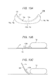
- FIG. 13A is a view describing a bottom spacer in an electric storage element according to a variation 4 of the embodiment of the present invention.
- FIG. 13B is a view describing the bottom spacer in the electric storage element according to the variation 4 of the embodiment of the present invention.
- FIG. 13C is a view describing the bottom spacer in the electric storage element according to the variation 4 of the embodiment of the present invention.
- FIG. 14 is a view describing a spacer in an electric storage element according to a variation 5 of the embodiment of the present invention.
- an aspect of the present invention provides an electric storage element including an electrode body having a positive electrode and a negative electrode, a case for housing the electrode body, an insulating member arranged in the case to insulate the electrode body from the case, and a spacer arranged in the case, wherein the spacer is arranged between the insulating member and the electrode body.
- the electric storage element has the configuration in which the spacer is arranged between the insulating member and the electrode body. That is, the spacer is fixed to the electrode body under the condition that it is sandwiched between the insulating member and the electrode body. Thus, the spacer is inserted into the case under the condition that it is fixed between the insulating member and the electrode body, whereby the electric storage element is provided.
- the spacer since the spacer is inserted into the case-under the condition that it is fixed to the electrode body with the insulating member, the spacer can be smoothly inserted into the case, while the spacer is prevented from being shifted in position in the case.
- the spacer may be configured to reduce a space between the electrode body and the case, and suppress the electrode body from moving in the case.
- the spacer having a relatively large volume is arranged along a bottom surface or a side surface of the case, and fixed to the electrode body under the condition that it is sandwiched between the insulating member and the electrode body.
- the spacer is inserted into the case under the condition that a relative position between the electrode body and the spacer is fixed with the insulating member. Therefore, even when the spacer is a bottom spacer which is inserted into the case ahead of the electrode body and arranged along the bottom surface of the case, the bottom spacer can be prevented from being shifted in position in the case.
- the insulating member may be arranged to cover the spacer and the electrode body.
- the electric storage element has the configuration in which the insulating member is arranged so as to cover the electrode body and the spacer. That is, the insulating member wraps around the electrode body and the spacer to fix the electrode body and the spacer. Therefore, the spacer is covered with the insulating member, fixed to the electrode body, and inserted into the case, so that the spacer can be smoothly inserted into the case, while the spacer is prevented from being shifted in position in the case.
- the insulating member may be a sheet-shaped member.
- the insulating member is the sheet-shaped member, it can easily wrap around the spacer and fix it to the electrode body.
- the insulating member may be bonded or welded to the spacer.
- the spacer can be effectively prevented from being shifted in position in the case.
- the spacer may have an internal part opposed to the electrode body, and two side parts arranged on both sides of the internal part, and at least one side part of the two side parts and the internal part may be connected through a curved surface.
- the spacer has a round tip end which comes in contact with the electrode body when it is fixed to the electrode body.
- the electrode body is prevented from being damaged with the tip end of the spacer.
- the spacer may have an internal part opposed to the electrode body, two side parts arranged on both sides of the internal part, and an external part arranged between the two side parts and opposed to the insulating member, and at least one side part of the two side parts and the external part may be connected through a curved surface.
- the spacer has a round corner part which comes in contact with the insulating member.
- the spacer may be an insulating member.
- the electrode body may have a coated region having active materials applied to surfaces of the positive electrode and the negative electrode, and a non-coated region not having the active material on the surface of the positive electrode or the negative electrode, the spacer may have a first part opposed to the non-coated region, and a second part opposed to the coated region, and the first part may be thicker than the second part.
- the first part of the spacer opposed to the non-coated region of the active material is thicker than the second part of the spacer opposed to the coated region of the active material.
- the performance of the electric storage element is not likely to be degraded even when compression is applied thereto.
- the first part of the spacer opposed to the non-coated region is formed to be thicker than the second part and thus compression is applied to the non-coated region, so that the vibration resistance can be enhanced, while the performance of the electric storage element is prevented from being degraded.
- the coated region is likely to be expanded due to repeated charge-discharge, and the performance of the electric storage element is likely to be degraded when it is excessively compressed. Therefore, the second part is formed to be thinner than the first part in the spacer, so that there can be provided a space for tolerating the expansion of the electrode body, and the performance of the electric storage element can be prevented from being degraded even when the electrode body is expanded.
- a clearance between the second part of the spacer and the coated region of the electrode body may be larger than a clearance between the first part of the spacer and the non-coated region of the electrode body.
- the spacer is formed in such a manner that the clearance between the spacer and the coated region of the electrode body is larger than the clearance between the spacer and the non-coated region of the electrode body. Therefore, even when the coated region of the electrode body is expanded due to the repeated charge-discharge, the expansion of the coated region of the electrode body can be tolerated because the clearance is large in the coated region. In addition, since the clearance is small in the non-coated region of the electrode body in which the performance of the electric storage element is not likely to be degraded due to the compression, the vibration resistance can be improved while the performance of the electric storage element is prevented from being degraded.
- the shape of the first part of the spacer on a side of the electrode body may follow an outer surface of the electrode body.
- the clearance can be minimized in the first part.
- the vibration resistance can be further improved in the first part of the spacer.
- the spacer may have the two first parts arranged at both ends in a longitudinal direction, the two second parts connected to the two first parts, respectively, and a third part thinner than the two second parts, between the two second parts.
- the spacer has the third part thinner than the second part, between the two second parts. That is, since the electrode body can be supported with the first part and the second part of the spacer, the third part provided between the two second parts and not used for supporting the electrode body can be thinned, so that costs can be reduced due to a reduction in amount of a component material.
- Another aspect of the present invention provides a method for manufacturing an electric storage element including an electrode body having a positive electrode and a negative electrode, a case for housing the electrode body, an insulating member arranged in the case to insulate the electrode body from the case, and a spacer arranged in the case, the method including an arranging step of arranging the spacer between the insulating member and the electrode body, and an inserting step of inserting the spacer into the case together with the insulating member and the electrode body.
- the spacer is arranged between the insulating member and the electrode body. That is, the spacer is fixed to the electrode body under the condition that it is sandwiched between the insulating member and the electrode body. Thus, the spacer is inserted into the case under the condition that it is fixed between the insulating member and the electrode body, whereby the electric storage element is provided.
- the spacer since the spacer is inserted into the case under the condition that it is fixed to the electrode body with the insulating member, the spacer can be smoothly inserted into the case, while the spacer is prevented from being shifted in position in the case.
- the spacer may be arranged between the insulating member and the electrode body such that the spacer and the electrode body are covered with the insulating member.
- the spacer is arranged between the insulating member and the electrode body such that the spacer and the electrode body are covered with the insulating member. That is, the insulating member wraps around the electrode body and the spacer to fix the electrode body and the spacer. Therefore, the spacer is covered with the insulating member, fixed to the electrode body, and inserted into the case, so that the spacer can be smoothly inserted into the case, while the spacer is prevented from being shifted in position in the case.
- the spacer may be set on the insulating member, the electrode body, which is formed into an oval shape by winding the elongated band-shaped positive electrode and negative electrode around a winding axis, may be put sideways, and the insulating member may be wound around the electrode body such that the spacer is arranged between the insulating member and the electrode body.
- FIG. 1 is a perspective view schematically showing an outer appearance of the electric storage element 10 according to an embodiment of the present invention.
- FIG. 2 is an exploded perspective view of the electric storage element 10 according to the embodiment of the present invention other than a case 100 . That is, FIG. 2 is a view showing components arranged in the case 100 of the electric storage element 10 .
- the electric storage element 10 serves as a secondary battery capable of charging and discharging electricity and more specifically, serves as a non-aqueous electrolyte battery such as a lithium-ion secondary battery.
- the electric storage element 10 is provided with the case 100 , and a lid plate 110 , a positive electrode terminal 200 , and a negative electrode terminal 300 which are provided in an upper part of the case 100 .
- the case 100 contains an electrode body 120 , a positive electrode collector 130 , a negative electrode collector 140 , side spacers 150 and 160 , a bottom spacer 170 , and an insulating member 180 .
- the electric storage element 10 is not limited to the non-aqueous electrolyte battery, and it may be a secondary battery other than the non-aqueous electrolyte battery, or may be a capacitor.
- the case 100 is a bottomed rectangular cylindrical case body made of metal, and an opening of the case body is covered with the metal lid plate 110 . That is, the case 100 can be hermetically sealed by being soldered with the lid plate 110 after the electrode body 120 and the like have been housed therein.
- the opening of the case 100 is defined as having a surface opposed to a bottom surface of the case 100 .
- the electrode body 120 is provided with a positive electrode, a negative electrode, and a separator although they are not described in detail, and serves as a member capable of storing electricity.
- the positive electrode is provided by forming an active material layer for the positive electrode on a surface of an elongated band-shaped positive electrode base member made of aluminum foil.
- the negative electrode is provided by forming an active material layer for the negative electrode on a surface of an elongated band-shaped negative electrode base member made of copper foil.
- the separator is a macro-porous sheet made of resin.
- the electrode body 120 is formed in such a manner that the above components are wound into the form of an oval shape as a whole in layers with the separator sandwiched between the negative electrode and the positive electrode.
- the positive electrode and the negative electrode are shifted in a width direction of the elongated band from each other with the separator interposed therebetween and wound around a winding axis along the width direction into the oval shape.
- the positive electrode collector 130 and the negative electrode collector 140 which extend in a direction vertical to a winding axis direction are arranged in ends of the electrode body 120 in the winding axis direction, respectively.
- the electrode body 120 has a flat part in which the positive electrode, the negative electrode, and the separator are laminated in a flat surface, and a curved part in which they are laminated in a curved surface.
- the electrode body 120 is housed in the case 100 in such a manner that the curved part is opposed to the bottom surface of the case 100 .
- the active material for the positive electrode includes a polyanion compound such as LiMPO 4 , LiMSiO 4 , or LiMBO 3 (M is one or more kinds of transition metal elements selected from Fe, Ni, Mn, Co, and the like), a spinel compound such as lithium titanate or lithium manganite, and a lithium transition metal oxide such as LiMO 2 (M is one or more kinds of transition metal elements selected from Fe, Ni, Mn, Co, and the like).
- a polyanion compound such as LiMPO 4 , LiMSiO 4 , or LiMBO 3
- M is one or more kinds of transition metal elements selected from Fe, Ni, Mn, Co, and the like
- a spinel compound such as lithium titanate or lithium manganite
- LiMO 2 lithium transition metal oxide
- the active material for negative electrode may be a well-known material as long as the material can absorb and emit lithium ions.
- the material includes lithium metal, lithium alloy (alloy containing lithium metal such as lithium-silicon, lithium-aluminum, lithium-lead, lithium-tin, lithium-aluminum-tin, lithium-gallium, or wood's alloy) as well as an alloy capable of absorbing and emitting lithium, a carbon material (such as black lead, non-graphitizable carbon, graphitizable carbon, low-temperature fired carbon, or amorphous carbon), silicon oxide, metal oxide, lithium metal oxide (such as Li 4 Ti 5 O 12 ), and polyphosphate compound.
- the oval shape is shown as the shape of the electrode body 120 in FIG. 2 , but the shape may be a circular shape or ellipsoidal shape.
- the positive electrode terminal 200 serves as an electrode terminal electrically connected to the positive electrode of the electrode body 120
- the negative electrode terminal 300 serves as an electrode terminal electrically connected to the negative electrode of the electrode body 120 . That is, each of the positive electrode terminal 200 and the negative electrode terminal 300 serves as the metal electrode terminal which discharges electricity stored in the electrode body 120 to an external space of the electric storage element 10 , and introduces electricity into the internal space of the electric storage element 10 in order to store electricity in the electrode body 120 .
- the positive electrode terminal 200 and the negative electrode terminal 300 are mounted on the lid plate 110 arranged in the upper part of the electrode body 120 .
- the positive electrode collector 130 is arranged between the positive electrode of the electrode body 120 and a side wall of the case 100 , and it is a conductive and rigid member electrically connected to the positive electrode terminal 200 and the positive electrode of the electrode body 120 .
- the positive electrode collector 130 is made of aluminum, similar to the positive electrode of the electrode body 120 .
- the negative electrode collector 140 is arranged between the negative electrode of the electrode body 120 and a side wall of the case 100 , and it is a conductive and rigid member electrically connected to the negative electrode terminal 300 and the negative electrode of the electrode body 120 .
- the negative electrode collector 140 is made of copper, similar to the negative electrode of the electrode body 120 .
- the side spacers 150 and 160 are arranged between the positive electrode collector 130 and the side wall of the case 100 , and between the negative electrode collector 140 and the side wall of the case 100 , respectively, and serve as elongated insulating members extending along the positive electrode collector 130 and the negative electrode collector 140 , respectively.
- the side spacers 150 and 160 are made of resin such as polypropylene (PP). That is, the side spacers 150 and 160 insulate the positive electrode collector 130 and the negative electrode collector 140 from the case 100 , respectively.
- the side spacers 150 and 160 fill a space between the positive electrode collector 130 and the case 100 and a space between the negative electrode collector 140 and the case 100 , respectively, so that the electrode body 120 is prevented from vibrating with the case 100 via the positive electrode collector 130 and the negative electrode collector 140 .
- the bottom spacer 170 is arranged between the electrode body 120 and the bottom surface of the case 100 and serves as an elongated insulating member extending along the winding axis direction of the electrode body 120 .
- the bottom spacer 170 is made of resin such as polypropylene (PP). More specifically, the bottom spacer 170 is arranged between the bottom surface of the case 100 and the curved part of the electrode body 120 . That is, the bottom spacer 170 insulates the electrode body 120 from the case 100 . Furthermore, the bottom spacer 170 fills a space between the electrode body 120 and the case 100 , so that the electrode body 120 is prevented from vibrating with the case 100 . A configuration of the bottom spacer 170 will be described in detail later.
- An insulating member 180 insulates the electrode body 120 from the case 100 . More specifically, the insulating member 180 is a sheet-shaped insulating member, and arranged so as to cover the bottom spacer 170 and the electrode body 120 . That is, the insulating member 180 is shaped like an exploded bag, and wraps around the bottom spacer 170 , the side spacers 150 and 160 , the positive electrode collector 130 , the negative electrode collector 140 , and a side surface of the electrode body 120 , from beneath the bottom spacer 170 . Thus, the bottom spacer 170 , and the side spacers 150 and 160 are arranged between the insulating member 180 and the electrode body 120 .
- the insulating member 180 when the insulating member 180 is formed, its size is adjusted so as to wrap around the bottom spacer 170 , the side spacers 150 and 160 , and the electrode body 120 .
- the insulating member 180 may not necessarily wrap around the whole of the electrode body 120 , but may be formed so as to only cover part of the electrode body 120 .
- the insulating member 180 may have any shape as long as it can be formed into the bag shape.
- FIG. 3 is a view showing that the bottom spacer 170 and the electrode body 120 covered with the insulating member 180 are to be inserted into the case 100 according to the embodiment of the present invention.
- the insulating member 180 covers the bottom spacer 170 , the side spacers 150 and 160 , the positive electrode collector 130 , the negative electrode collector 140 , and the electrode body 120 so as to wrap around them from beneath the bottom spacer 170 .
- a component group covered with the insulating member 180 is inserted into the case 100 .
- FIG. 4 is a view showing a positional relationship between the electrode body 120 and the bottom spacer 170 in the electric storage element 10 according to the embodiment of the present invention.
- the positive electrode collector 130 , the negative electrode collector 140 , the side spacers 150 and 160 , and the insulating member 180 are not shown.
- FIGS. 5A and 5B are views showing the configuration of the bottom spacer 170 according to the embodiment of the present invention. More specifically, FIG. 5A is an oblique perspective view of an outer appearance of the bottom spacer 170 , and FIG. 5B is a view of the bottom spacer 170 taken from lower left in FIG. 5A .
- a non-coated region A 1 in which the active material is not applied to the positive electrode or the negative electrode is provided in each end of the electrode body 120 in the winding axis direction, and a-coated region A 2 in which the active material is applied to each of the positive electrode and the negative electrode is provided between the non-coated regions A 1 in the center of the electrode body 120 in the winding axis direction.
- the bottom spacer 170 has two first parts 171 opposed to the non-coated regions A 1 of the electrode body 120 , and a second part 172 opposed to the coated region A 2 of the electrode body 120 .
- a cross-sectional shape of the first part 171 is different from a cross-sectional shape of the second part 172 when viewed from a plane perpendicular to the winding axis direction of the electrode body 120 .
- the first part 171 is formed to be thicker than the second part 172 . That is, a clearance between the second part 172 of the bottom spacer 170 and the coated region A 2 of the electrode body 120 is larger than a clearance between the first part 171 of the bottom spacer 170 and the non-coated region A 1 of the electrode body 120 .
- the first part 171 has an internal part 171 a , two side parts 171 b , and an external part 171 c.
- the internal part 171 a is opposed to the electrode body 120 and has a shape along an outer surface of the electrode body 120 . That is, a shape of the first part 171 of the bottom spacer 170 on the side of the electrode body 120 follows an outer surface of the non-coated region A 1 of the electrode body 120 . More specifically, the internal part 171 a has a dented curved shape.
- the side part 171 b has a flat surface provided on each side of the internal part 171 a . That is, a side shape of the first part 171 of the bottom spacer 170 follows an internal side surface of the case 100 .
- the external part 171 c is a flat surface arranged between the two side parts 171 b so as to be opposed to the insulating member 180 . That is, a bottom shape of the first part 171 of the bottom spacer 170 follows an internal bottom surface of the case 100 .
- At least one side part 171 b of the two side parts 171 b and the internal part 171 a are connected through a curved surface. That is, as shown in FIG. 5B , the two side parts 171 b and the internal part 171 a are connected through curved surfaces R 1 and R 2 , respectively.
- the curved surfaces R 1 and R 2 may have any shape as long as they are curved, and for example, each of them may have an arc shaped cross-section having a radius of 1 mm to 2 mm.
- At least one side part 171 b of the two side parts 171 b and the external part 171 c are connected through a curved surface. That is, as shown in FIG. 5B , the two side parts 171 b and the external part 171 c are connected through curved surfaces R 3 and R 4 , respectively.
- the curved surfaces R 3 and R 4 may have any shape as long as they are curved, and for example, each of them may have an arc shaped cross-section having a radius of 1 mm to 3 mm.
- the second part 172 has an internal part 172 a , two side parts 172 b , and an external part 172 c.
- the internal part 172 a is opposed to the electrode body 120 and has a shape along an outer surface of the electrode body 120 . That is, a shape of the second part 172 of the bottom spacer 170 on the side of the electrode body 120 follows an outer surface of the coated region A 2 of the electrode body 120 . More specifically, the internal part 172 a has a dented curved shape.
- the side part 172 b is provided on each side of the internal part 172 a. That is, a side shape of the second part 172 of the bottom spacer 170 follows an internal side surface of the case 100 .
- the external part 172 c is a surface arranged between the two side parts 172 b so as to be opposed to the insulating member 180 . That is, a bottom shape of the second part 172 of the bottom spacer 170 follows an internal bottom surface of the case 100 .
- the curved surface may have any shape as long as it is curved, and for example, it may have an arc shaped cross-section having a radius of 1 mm to 2 mm.
- the curved surface may have any shape as long as it is curved, and for example, it may have an arc shaped cross-section having a radius of 1 mm to 3 mm.
- the curved surface is provided at each end of the bottom spacer 170 in a width direction, at each tip end of the side part arranged so as to extend in a longitudinal direction of the bottom spacer 170 along the side of the electrode body 120 .
- an internal part of each of the side spacers 150 and 160 opposed to the electrode body 120 , and two side parts arranged on both sides of the internal part thereof may be connected though curved surfaces.
- the two side parts of each of the side spacers 150 and 160 and an external part arranged between the two side parts so as to be opposed to the insulating member 180 may be connected through curved surfaces.
- the bottom spacer 170 is arranged between the insulating member 180 and the electrode body 120 . That is, the bottom spacer 170 having a relatively large volume which is arranged along the bottom surface of the case 100 , is fixed to the electrode body 120 under the condition that it is sandwiched between the insulating member 180 and the electrode body 120 .
- the bottom spacer 170 is inserted into the case 100 under the condition that it is fixed between the insulating member 180 and the electrode body 120 (that is, under the condition that a relative position between the electrode body 120 and the bottom spacer 170 is fixed with the insulating member 180 ), whereby the electric storage element 10 is provided.
- the bottom spacer 170 is inserted into the case 100 ahead of the electrode body 120 and pushed by the electrode body 120 toward the bottom of the case 100 under the condition that it is fixed to the electrode body 120 with the insulating member 180 , so that the bottom spacer 170 can be smoothly inserted into the case 100 , while the bottom spacer 170 is prevented from being shifted in position in the case 100 .
- the electric storage element 10 has the configuration in which the insulating member 180 is arranged so as to cover the electrode body 120 and the bottom spacer 170 . That is, the insulating member 180 fixes the electrode body 120 and the bottom spacer 170 while wrapping around the electrode body 120 and the bottom spacer 170 . Therefore, the bottom spacer 170 is inserted into the case 100 while it is covered with the insulating member 180 and fixed to the electrode body 120 , so that the bottom spacer 170 can be smoothly inserted into the case 100 , while-the bottom spacer 170 is prevented from being shifted in position in the case 100 .
- the insulating member 180 is the sheet-shaped member, it can wrap around the bottom spacer 170 and fix it to the electrode body 120 with ease.
- the bottom spacer 170 has the round tip end which comes in contact with the electrode body 120 when it is fixed to the electrode body 120 .
- the electrode body 120 can be prevented from being damaged with the tip end of the bottom spacer 170 .
- the bottom spacer 170 has the round corner part which comes in contact with the insulating member 180 .
- the insulating member 180 can be prevented from being damaged with the corner part of the bottom spacer 170 .
- the bottom spacer 170 is the insulating member, so that even in a case where the insulating member 180 is damaged when the bottom spacer 170 is wrapped with the insulating member 180 and fixed to the electrode body 120 , insulating properties between the electrode body 120 and the case 100 can be ensured.
- the first part 171 of the bottom spacer 170 opposed to the non-coated region A 1 of the active-material is thicker than the second part 172 of the bottom spacer 170 opposed to the coated region A 2 of the active material.
- the non-coated region A 1 is a region in which performance of the electric storage element 10 is not likely to be degraded even when compression is applied thereto.
- the first part 171 opposed to the non-coated region A 1 is formed to be thicker than the second part 172 in the bottom spacer 170 and compression is applied to the non-coated region A 1 , so that the vibration resistance can be enhanced while the performance of the electric storage element 10 is prevented from being degraded.
- the coated region A 2 is likely to be expanded due to repeated charge-discharge, so that when compression is excessively applied thereto, the performance of the electric storage element 10 is likely to be degraded.
- the second part 172 is formed to be thinner than the first part 171 in the bottom spacer 170 , a space for tolerating the expansion of the electrode body 120 can be provided, so that even when the electrode body 120 is expanded, the performance of the electric storage element 10 can be prevented from being degraded.
- the clearance between the bottom spacer 170 and the coated region A 2 of the electrode body 120 is larger than the clearance between the bottom spacer 170 and the non-coated region A 2 of the electrode body 120 . Therefore, even when the coated region A 2 of the electrode body 120 is expanded due to the repeated charge-discharge, the expansion of the coated region A 2 of the electrode body 120 can be tolerated because the clearance is large in the coated region A 2 .
- the electrode body 120 has the small clearance in the non-coated region A 1 in which degradation in performance of the electric storage element 10 is not likely to be caused by the compression, so that the vibration resistance can be improved, while the performance of the electric storage element 10 is not degraded.
- the clearance can be minimized in the first part 171 .
- the vibration resistance in the first part 171 can be further improved in the bottom spacer 170 .
- FIG. 6 is a flowchart showing one example of the method for manufacturing the electric storage element 10 according to the embodiment of the present invention.
- FIGS. 7A to 7C are views describing the method for manufacturing the electric storage element 10 according to the embodiment of the present invention.
- the lid plate 110 the positive electrode collector 130 , the negative electrode collector 140 , and the side spacers 150 and 160 are not shown.
- the bottom spacer 170 is arranged between the insulating member 180 and the electrode body 120 (S 102 ).
- the bottom spacer 170 is set on the insulating member 180 , and attached thereto (fixed with a bonding agent or a bonding tape). Alternatively, ultrasonic welding may be used.
- the electrode body 120 is set sideways on the insulating member 180 adjacent to the bottom spacer 170 , with its bottom opposed to the bottom spacer 170 .
- the insulating member 180 is lifted together with the bottom spacer 170 so as to be wound around the electrode body 120 .
- the tip end of the bottom spacer 170 abuts on the electrode body 120 as shown in FIG. 7B , but the electrode body 120 can be prevented from being damaged because the tip end of the bottom spacer 170 is rounded.
- the insulating member 180 is wound around the electrode body 120 so that the bottom spacer 170 and the electrode body 120 are covered with the insulating member 180 .
- the bottom spacer 170 is arranged between the insulating member 180 and the electrode body 120 .
- the bottom spacer 170 is inserted into the case 100 together with the insulating member 180 and the electrode body 120 (S 104 ).
- the case 100 is arranged sideways so that its opening faces to a horizontal direction.
- the component group having the bottom spacer 170 and the electrode body 120 wrapped with the insulating member 180 is horizontally inserted into the case 100 through the opening of the case 100 .
- the case 100 since the case 100 is arranged sideways, the case 100 can be easily held by strong force, and the component group having the bottom spacer 170 and the electrode-body 120 wrapped with the insulating member 180 can be easily inserted into the case 100 .
- the bottom spacer 170 is disposed between the insulating member 180 and the electrode body 120 . That is, the bottom spacer 170 is fixed to the electrode body 120 under the condition that it is sandwiched between the insulating member 180 and the electrode body 120 . Thus, the bottom spacer 170 is inserted into the case 100 under the condition that it is fixed between the insulating member 180 and the electrode body 120 , whereby the electric storage element 10 is provided.
- the bottom spacer 170 is inserted into the case 100 under the condition that it is fixed to the electrode body 120 with the insulating member 180 , the bottom spacer 170 can be smoothly inserted into the case 100 , while the bottom spacer 170 is prevented from being shifted in position in the case 100 .
- the bottom spacer 170 is arranged between the insulating member 180 and the electrode body 120 such that the electrode body 120 and the bottom spacer 170 are covered with the insulating member 180 . That is, the electrode body 120 and the bottom spacer 170 are fixed in such a manner that the insulating member 180 wraps around the electrode body 120 and the bottom spacer 170 . Therefore, since the bottom spacer 170 is inserted into the case 100 under the condition that it is covered with the insulating member 180 and fixed to the electrode body 120 , the bottom spacer 170 can be smoothly inserted into the case 100 , while the bottom spacer 170 is prevented from being shifted in position in the case 100 .
- the insulating member 180 is the sheet-shaped member.
- the insulating member is a bag-shaped member.
- FIG. 8 is a view showing a configuration of an electric storage element 11 according to the variation 1 of the embodiment of the present invention.
- a configuration in the case 100 is shown, while the case 100 is not shown.
- the electric storage element 11 is provided with a bag-shaped insulating member 181 having an opening in its upper part.
- the insulating member 181 is an insulating member provided by forming an insulating sheet into a bag shape.
- the insulating member 181 is arranged so as to cover the bottom spacer 170 and the electrode body 120 . That is, the electrode body 120 , the positive electrode collector 130 , the negative electrode collector 140 , the side spacers 150 and 160 , and the bottom spacer 170 are housed in the insulating member 181 , and then inserted into the case 100 .
- the insulating member 181 When the insulating member 181 is formed, its size is adjusted so as to be able to house the electrode body 120 , the positive electrode collector 130 , the negative electrode collector 140 , the side spacers 150 and 160 , and the bottom spacer 170 therein. In addition, the insulating member 181 may not have to entirely house the electrode body 120 , and it may be formed so as to only cover part of a lower part of the electrode body 120 .
- the bag-shaped insulating member 181 is arranged so as to cover the electrode body 120 and the spacers (side spacers 150 and 160 and the bottom spacer 170 ). That is, the insulating member 181 wraps around the electrode body 120 and the spacers, and fixes the electrode body 120 and the spacers. Therefore, since the spacers are inserted into the case 100 under the condition that they are wrapped with the insulating member 181 and fixed to the electrode body 120 , the spacers can be smoothly inserted into the case 100 , while the spacers are prevented from being shifted in position in the case 100 .
- the insulating member 180 covers both of the bottom spacer 170 and the side spacers 150 and 160 .
- the insulating member is arranged so as to cover the bottom spacer 170 and/or the side spacers 150 and 160 .
- FIGS. 9 to 11 are views each showing a configuration of an electric storage element according to the variation 2 of the embodiment of the present invention.
- FIGS. 9 and 10 a configuration in the case 100 is shown, while the case 100 is not shown.
- an electric storage element 12 is provided with a rectangular sheet-shaped insulating member 182 .
- the insulating member 182 is arranged so as to cover the bottom spacer 170 and the electrode body 120 . That is, the electrode body 120 , the positive electrode collector 130 , the negative electrode collector 140 , the side spacers 150 and 160 , and the bottom spacer 170 are covered so as to be wrapped with the insulating member 182 from beneath the electrode body 120 .
- the insulating member 182 When the insulating member 182 is formed, its size is adjusted so as to wrap around the electrode body 120 , the positive electrode collector 130 , the negative electrode collector 140 , the side spacers 150 and 160 , and the bottom spacer 170 .
- the component group may be provided in such a manner that the side spacers 150 and 160 are mounted on the electrode body 120 , the electrode body 120 and the side spacers 150 and 160 are wrapped with the insulating member 182 bonded or ultrasonically welded to the spacer 170 , and the insulating member 182 is thermally welded to the side spacers 150 and 160 .
- the insulating member 182 does not have to wrap around the entire electrode body 120 , but it may cover only part of the electrode body 120 .
- an electric storage element 13 is provided with a rectangular sheet-shaped insulating member 183 .
- the insulating member 183 is arranged so as to cover the side spacers 150 and 160 , and the electrode body 120 . That is, the electrode body 120 , the positive electrode collector 130 , the negative electrode collector 140 , the side spacers 150 and 160 , and the bottom spacer 170 are covered and wrapped with the insulating member 183 from the side of the electrode body 120 .
- an end of the insulating member 183 is fixed with an adhesive tape 184 , and inserted into the case 100 .
- the insulating member 183 When the insulating member 183 is formed, its size is-adjusted so as to wrap around the electrode body 120 , the positive electrode collector 130 , the negative electrode collector 140 , the side spacers 150 and 160 , and the bottom spacer 170 . In addition, the insulating member 183 does not have to wrap around the-entire electrode body 120 , but it may cover only part of the electrode body 120 .
- corner parts of the side spacers 150 and 160 which come in contact with the electrode body 120 or the insulating member 183 are curved, similar to the bottom spacer 170 . That is, an internal part of each of the side spacers 150 and 160 opposed to the electrode body 120 , and two side parts arranged on both sides of the internal part are preferably connected through curved surfaces. It is preferable that the two side parts of each of the side spacers 150 and 160 and an external part arranged between the two side parts provided opposed to the insulating member 183 are connected through curved surfaces.
- the insulating members 182 and 183 are arranged so as to cover the electrode body 120 and the spacers (side spacers 150 and 160 and bottom spacer 170 ) from beneath and from the side, respectively. That is, each of the insulating members 182 and 183 fixes the electrode body 120 and the spacers by wrapping the electrode body 120 and the spacers from beneath or from the side.
- the spacers are covered with each of the insulating members 182 and 183 from beneath or from the side and fixed to the electrode body 120 , and then inserted into the case 100 , so that the spacers can be smoothly inserted into the case 100 , while the spacers are prevented from being shifted in position in the case 100 .
- the bottom spacer 170 is composed of the two first parts 171 , and the second part 172 sandwiched between the two first parts 171 .
- the bottom spacer 170 further includes a third part.
- FIG. 12 is a view showing a configuration of a bottom spacer 170 A of an electric storage element according to the variation 3 of the embodiment of the present invention.
- the bottom spacer 170 A has the two first parts 171 arranged in both ends in a longitudinal direction, and two second parts 173 connected to the two first parts 171 , respectively.
- the bottom spacer 170 A has a third part 174 between the two second parts 173 .
- the third part 174 is a flat portion thinner than the two second parts 173 . That is, the bottom spacer 170 A has a configuration provided by forming a thinner center part in the center of the bottom spacer 170 in the above embodiment.
- the shape of the third part 174 is not limited to the flat shape, and may be any shape such as a curved shape. Furthermore, the first part 171 , the second part 173 , and the third part 174 may be made of the same material, or may be made of different materials.
- the bottom spacer 170 A of the electric storage element has the third part 174 thinner than the second part 173 , between the two second parts 173 . That is, the electrode body 120 can be supported with the first parts 171 and the second parts 173 of the bottom spacer 170 A, so that the third part 174 which is not used for supporting the electrode body 120 can be thinned, and costs can be reduced due to a reduction in amount of a component material.
- the side part and the external part of the first part, and the side part and the external part of the second part in the bottom spacer have the flat shape, but according to this variation 4, each of a side part and an external part of a bottom spacer has a curved shape.
- FIGS. 13A to FIG. 13C are views each describing a bottom spacer 170 B of an electric storage element according to the variation 4 of the embodiment of the present invention. More specifically, FIG. 13A is a view corresponding to the bottom spacer 170 in FIG. 5B , and FIGS. 13B and 13C are views corresponding to the method for manufacturing the electric storage element 10 in FIGS. 7A and 7B , respectively.
- the bottom spacer 170 B is provided with a first part 175 and a second part 176 .
- the first part 175 has an internal part 175 a as an upper surface, two side parts 175 b as side surfaces, and an external part 175 c as a bottom surface.
- the second part 176 has an internal part 176 a as an upper surface, two side parts 176 b as side surfaces, and an external part 176 c as a bottom surface.
- Each of the two side parts 175 b , the external part 175 c , the two side parts 176 b , and the external part 176 c has a curved shape. That is, the side part 175 b has a curved surface arranged on each side of the internal part 175 a , and the external part 175 c has a curved surface arranged between the two side parts 175 b and opposed to the insulating member 180 . Furthermore, the side part 176 b has a curved surface arranged on each side of the internal part 176 a , and the external part 176 c has a curved surface arranged between the two side parts 176 b and opposed to the insulating member 180 .
- the bottom spacer 170 B is put on the insulating member 180 adjacent to the electrode body 120 , and as shown in FIG. 13C , the insulating member 180 is lifted together with the bottom spacer 170 B so as to be wound around the electrode body 120 , so that the insulating member 180 is wound around the electrode body 120 .
- the insulating member 180 can be smoothly bent.
- the bottom spacer 170 B is inserted into the case 100 together with insulating member 180 and the electrode body 120 .
- the side part and the external part of the bottom spacer 170 B need not entirely have the curved shape, but the curved shape may be partially provided in one part of the two side parts 175 b , the external part 175 c , the two side parts 176 b , and the external part 176 c.
- a spacer has a side part functioning as a side spacer, and a bottom part functioning as a bottom spacer.
- a spacer 165 of an electric storage element according to the variation 5 has a side part 165 a and a bottom part 165 b .
- a configuration of this electric storage element other than this spacer is similar to the electric storage element shown in FIG. 9 .
- the side part 165 a is arranged along a side wall of a case.
- the bottom part 165 b is arranged along a bottom surface of the case.
- the side part 165 a extends in a direction roughly perpendicular to the bottom part 165 b .
- the spacer 165 is mounted on the electrode body 120 shown in FIG. 9 , and then the bottom part 165 b is wrapped with the insulating member 182 together with the electrode body 120 .
- the bottom spacer 170 has the first part 171 , and the second part 172 thinner than the first part 171 .
- the bottom spacer 170 may have the first part 171 , and the second part 172 lower in hardness than the first part 171 .
- the bottom spacer 170 may have only the first part 171 without having the second part 172 . In these configuration also, the bottom spacer 170 can support the electrode body 120 while tolerating the expansion of the electrode body 120 .
- the preset invention can be applied to the electric storage element in which the spacer can be smoothly inserted into the case, while the spacer can be prevented from being shifted in position in the case.
Landscapes
- Engineering & Computer Science (AREA)
- Power Engineering (AREA)
- Chemical & Material Sciences (AREA)
- Chemical Kinetics & Catalysis (AREA)
- Electrochemistry (AREA)
- General Chemical & Material Sciences (AREA)
- Microelectronics & Electronic Packaging (AREA)
- Manufacturing & Machinery (AREA)
- Secondary Cells (AREA)
- Cell Separators (AREA)
- Electric Double-Layer Capacitors Or The Like (AREA)
- Connection Of Batteries Or Terminals (AREA)
Abstract
An electric storage element includes an electrode body including a positive electrode and a negative electrode, the electrode body including a coated region, which includes active materials applied to surfaces of the positive electrode and the negative electrode, and a non-coated region not including the active material on the surface of the positive electrode or the negative electrode, a case including a case body for housing the electrode body and a lid plate that covers an opening of the case body, the case body including a bottom wall having a long side and a short side, the case body further including a side wall standing on the short side of the bottom wall, the lid plate being formed with an electrode terminal, and an insulating member arranged in the case to insulate the electrode body from the case.
Description
The present application is a Continuation Application of U.S. patent application Ser. No. 13/765,405, now U.S. Pat. No. 9,214,652, filed on Feb. 12, 2013, which is based on and claims priority from Japanese Patent Application No. 2012-030821, filed on Feb. 15, 2012, and Japanese Patent Application No. 2013-004871, filed on Jan. 15, 2013, the entire contents of which are incorporated herein by reference.
1. Field of the Invention
The present invention relates to an electric storage element provided with an electrode body having a positive electrode and a negative electrode, an insulating member for insulating the electrode body from a case, and a spacer arranged in the case, and a method for manufacturing the electric storage element.
2. Description of the Related Art
As an approach to global environmental issues, it becomes increasingly important to convert a gasoline car to an electric car. Thus, an electric car having an electric storage element such as a lithium-ion secondary battery as its power source has been developed.
An electric storage element houses an electrode body having a positive electrode and a negative electrode in a case. Because of a space between the electrode body and the case, extra electrolyte solution may be needed. The space may cause a swing or vibration of the electrode body in the case. Conventionally, a battery has been proposed in which a spacer is provided between the electrode body and the case so that the space between the electrode body and the case can be reduced (for example, refer to JP-A-2006-40899).
However, according to the conventional electric storage element, it is necessary to insert the spacer into the case in addition to the electrode body when the electric storage element is manufactured, which complicates a step of inserting them into the case. In addition, after the spacer has been inserted into the case, the spacer could be shifted in position in the case.
An aspect of the present invention provides an electric storage element including an electrode body having a positive electrode and a negative electrode, a case for housing the electrode body, an insulating member arranged in the case to insulate the electrode body from the case, and a spacer arranged in the case, wherein the spacer is arranged between the insulating member and the electrode body.
The foregoing and other features of the invention will become apparent to one skilled in the art to which the present invention relates upon consideration of the invention with reference to the accompanying drawings, wherein:
As described above, an aspect of the present invention provides an electric storage element including an electrode body having a positive electrode and a negative electrode, a case for housing the electrode body, an insulating member arranged in the case to insulate the electrode body from the case, and a spacer arranged in the case, wherein the spacer is arranged between the insulating member and the electrode body.
With this configuration, the electric storage element has the configuration in which the spacer is arranged between the insulating member and the electrode body. That is, the spacer is fixed to the electrode body under the condition that it is sandwiched between the insulating member and the electrode body. Thus, the spacer is inserted into the case under the condition that it is fixed between the insulating member and the electrode body, whereby the electric storage element is provided. Thus, since the spacer is inserted into the case-under the condition that it is fixed to the electrode body with the insulating member, the spacer can be smoothly inserted into the case, while the spacer is prevented from being shifted in position in the case.
The spacer may be configured to reduce a space between the electrode body and the case, and suppress the electrode body from moving in the case.
With this configuration, the spacer having a relatively large volume is arranged along a bottom surface or a side surface of the case, and fixed to the electrode body under the condition that it is sandwiched between the insulating member and the electrode body. Thus, the spacer is inserted into the case under the condition that a relative position between the electrode body and the spacer is fixed with the insulating member. Therefore, even when the spacer is a bottom spacer which is inserted into the case ahead of the electrode body and arranged along the bottom surface of the case, the bottom spacer can be prevented from being shifted in position in the case.
The insulating member may be arranged to cover the spacer and the electrode body.
The electric storage element has the configuration in which the insulating member is arranged so as to cover the electrode body and the spacer. That is, the insulating member wraps around the electrode body and the spacer to fix the electrode body and the spacer. Therefore, the spacer is covered with the insulating member, fixed to the electrode body, and inserted into the case, so that the spacer can be smoothly inserted into the case, while the spacer is prevented from being shifted in position in the case.
The insulating member may be a sheet-shaped member.
With this configuration, since the insulating member is the sheet-shaped member, it can easily wrap around the spacer and fix it to the electrode body.
The insulating member may be bonded or welded to the spacer.
With this configuration, the spacer can be effectively prevented from being shifted in position in the case.
The spacer may have an internal part opposed to the electrode body, and two side parts arranged on both sides of the internal part, and at least one side part of the two side parts and the internal part may be connected through a curved surface.
With this configuration, at least one side part and the internal part of the spacer are connected through the curved surface. That is, the spacer has a round tip end which comes in contact with the electrode body when it is fixed to the electrode body. Thus, when the spacer is fixed to the electrode body, the electrode body is prevented from being damaged with the tip end of the spacer.
The spacer may have an internal part opposed to the electrode body, two side parts arranged on both sides of the internal part, and an external part arranged between the two side parts and opposed to the insulating member, and at least one side part of the two side parts and the external part may be connected through a curved surface.
With this configuration, at least one side part and the external part of the spacer are connected through the curved surface. That is, the spacer has a round corner part which comes in contact with the insulating member. Thus, even when the spacer and the insulating member are brought into contact with each other due to vibration or the like, the insulating member can be prevented from being damaged with the corner part of the spacer.
The spacer may be an insulating member.
With this configuration even when the insulating member is damaged while the spacer is wrapped with the insulating member and fixed to the electrode body, an insulating property can be kept between the electrode body and the case.
The electrode body may have a coated region having active materials applied to surfaces of the positive electrode and the negative electrode, and a non-coated region not having the active material on the surface of the positive electrode or the negative electrode, the spacer may have a first part opposed to the non-coated region, and a second part opposed to the coated region, and the first part may be thicker than the second part.
With this configuration, the first part of the spacer opposed to the non-coated region of the active material is thicker than the second part of the spacer opposed to the coated region of the active material. In the non-coated region, the performance of the electric storage element is not likely to be degraded even when compression is applied thereto. According to this electric storage element, in order to enhance vibration resistance thereof, the first part of the spacer opposed to the non-coated region is formed to be thicker than the second part and thus compression is applied to the non-coated region, so that the vibration resistance can be enhanced, while the performance of the electric storage element is prevented from being degraded. In addition, the coated region is likely to be expanded due to repeated charge-discharge, and the performance of the electric storage element is likely to be degraded when it is excessively compressed. Therefore, the second part is formed to be thinner than the first part in the spacer, so that there can be provided a space for tolerating the expansion of the electrode body, and the performance of the electric storage element can be prevented from being degraded even when the electrode body is expanded.
A clearance between the second part of the spacer and the coated region of the electrode body may be larger than a clearance between the first part of the spacer and the non-coated region of the electrode body.
With this configuration, the spacer is formed in such a manner that the clearance between the spacer and the coated region of the electrode body is larger than the clearance between the spacer and the non-coated region of the electrode body. Therefore, even when the coated region of the electrode body is expanded due to the repeated charge-discharge, the expansion of the coated region of the electrode body can be tolerated because the clearance is large in the coated region. In addition, since the clearance is small in the non-coated region of the electrode body in which the performance of the electric storage element is not likely to be degraded due to the compression, the vibration resistance can be improved while the performance of the electric storage element is prevented from being degraded.
The shape of the first part of the spacer on a side of the electrode body may follow an outer surface of the electrode body.
With this configuration, since the shape of the first part of the spacer on the side of the electrode body follows the shape of the electrode body, the clearance can be minimized in the first part. As a result, the vibration resistance can be further improved in the first part of the spacer.
The spacer may have the two first parts arranged at both ends in a longitudinal direction, the two second parts connected to the two first parts, respectively, and a third part thinner than the two second parts, between the two second parts.
With this configuration, the spacer has the third part thinner than the second part, between the two second parts. That is, since the electrode body can be supported with the first part and the second part of the spacer, the third part provided between the two second parts and not used for supporting the electrode body can be thinned, so that costs can be reduced due to a reduction in amount of a component material.
Another aspect of the present invention provides a method for manufacturing an electric storage element including an electrode body having a positive electrode and a negative electrode, a case for housing the electrode body, an insulating member arranged in the case to insulate the electrode body from the case, and a spacer arranged in the case, the method including an arranging step of arranging the spacer between the insulating member and the electrode body, and an inserting step of inserting the spacer into the case together with the insulating member and the electrode body.
With this configuration, the spacer is arranged between the insulating member and the electrode body. That is, the spacer is fixed to the electrode body under the condition that it is sandwiched between the insulating member and the electrode body. Thus, the spacer is inserted into the case under the condition that it is fixed between the insulating member and the electrode body, whereby the electric storage element is provided. Thus, since the spacer is inserted into the case under the condition that it is fixed to the electrode body with the insulating member, the spacer can be smoothly inserted into the case, while the spacer is prevented from being shifted in position in the case.
In the arranging step, the spacer may be arranged between the insulating member and the electrode body such that the spacer and the electrode body are covered with the insulating member.
With this configuration, the spacer is arranged between the insulating member and the electrode body such that the spacer and the electrode body are covered with the insulating member. That is, the insulating member wraps around the electrode body and the spacer to fix the electrode body and the spacer. Therefore, the spacer is covered with the insulating member, fixed to the electrode body, and inserted into the case, so that the spacer can be smoothly inserted into the case, while the spacer is prevented from being shifted in position in the case.
In the arranging step, the spacer may be set on the insulating member, the electrode body, which is formed into an oval shape by winding the elongated band-shaped positive electrode and negative electrode around a winding axis, may be put sideways, and the insulating member may be wound around the electrode body such that the spacer is arranged between the insulating member and the electrode body.
With this configuration, manufacturing efficiency can be improved.
Preferred embodiments of the present invention will be described. Hereinafter, a description will be given of an electric storage element and a method for manufacturing the electric storage element according to an embodiment of the present invention, with reference to the drawings. In addition, each embodiment which will be described below shows one preferred specific example of the present invention. Numeric values, shapes, materials, components, and arranged positions and connected configurations of the components shown in the following embodiment are illustrative only, and do not limit the present invention.
First, a configuration of an electric storage element 10 will be described.
The electric storage element 10 serves as a secondary battery capable of charging and discharging electricity and more specifically, serves as a non-aqueous electrolyte battery such as a lithium-ion secondary battery.
As shown in FIGS. 1 and 2 , the electric storage element 10 is provided with the case 100, and a lid plate 110, a positive electrode terminal 200, and a negative electrode terminal 300 which are provided in an upper part of the case 100. In addition, the case 100 contains an electrode body 120, a positive electrode collector 130, a negative electrode collector 140, side spacers 150 and 160, a bottom spacer 170, and an insulating member 180.
In addition, a liquid such as an electrolyte solution is encapsulated in the case 100 of the electric storage element 10, but the liquid is not shown in the drawing. Incidentally, the electric storage element 10 is not limited to the non-aqueous electrolyte battery, and it may be a secondary battery other than the non-aqueous electrolyte battery, or may be a capacitor.
The case 100 is a bottomed rectangular cylindrical case body made of metal, and an opening of the case body is covered with the metal lid plate 110. That is, the case 100 can be hermetically sealed by being soldered with the lid plate 110 after the electrode body 120 and the like have been housed therein. In this embodiment, the opening of the case 100 is defined as having a surface opposed to a bottom surface of the case 100.
The electrode body 120 is provided with a positive electrode, a negative electrode, and a separator although they are not described in detail, and serves as a member capable of storing electricity. The positive electrode is provided by forming an active material layer for the positive electrode on a surface of an elongated band-shaped positive electrode base member made of aluminum foil. The negative electrode is provided by forming an active material layer for the negative electrode on a surface of an elongated band-shaped negative electrode base member made of copper foil. The separator is a macro-porous sheet made of resin. The electrode body 120 is formed in such a manner that the above components are wound into the form of an oval shape as a whole in layers with the separator sandwiched between the negative electrode and the positive electrode.
More specifically, the positive electrode and the negative electrode are shifted in a width direction of the elongated band from each other with the separator interposed therebetween and wound around a winding axis along the width direction into the oval shape. Thus, by forming a region having no active material applied, in an edge part of each of the positive electrode and the negative electrode in their shifted direction, the aluminum foil of the positive electrode base member on which the active material is not formed is exposed to one end of the winding axis, and the copper foil of the negative electrode base member on which the active material is not formed is exposed to another end of the winding axis. In addition, the positive electrode collector 130 and the negative electrode collector 140 which extend in a direction vertical to a winding axis direction are arranged in ends of the electrode body 120 in the winding axis direction, respectively.
In addition, the electrode body 120 has a flat part in which the positive electrode, the negative electrode, and the separator are laminated in a flat surface, and a curved part in which they are laminated in a curved surface. Thus, the electrode body 120 is housed in the case 100 in such a manner that the curved part is opposed to the bottom surface of the case 100.
Here, the active material for the positive electrode includes a polyanion compound such as LiMPO4, LiMSiO4, or LiMBO3 (M is one or more kinds of transition metal elements selected from Fe, Ni, Mn, Co, and the like), a spinel compound such as lithium titanate or lithium manganite, and a lithium transition metal oxide such as LiMO2 (M is one or more kinds of transition metal elements selected from Fe, Ni, Mn, Co, and the like).
In addition, the active material for negative electrode may be a well-known material as long as the material can absorb and emit lithium ions. For example, the material includes lithium metal, lithium alloy (alloy containing lithium metal such as lithium-silicon, lithium-aluminum, lithium-lead, lithium-tin, lithium-aluminum-tin, lithium-gallium, or wood's alloy) as well as an alloy capable of absorbing and emitting lithium, a carbon material (such as black lead, non-graphitizable carbon, graphitizable carbon, low-temperature fired carbon, or amorphous carbon), silicon oxide, metal oxide, lithium metal oxide (such as Li4Ti5O12), and polyphosphate compound.
The oval shape is shown as the shape of the electrode body 120 in FIG. 2 , but the shape may be a circular shape or ellipsoidal shape.
The positive electrode terminal 200 serves as an electrode terminal electrically connected to the positive electrode of the electrode body 120, and the negative electrode terminal 300 serves as an electrode terminal electrically connected to the negative electrode of the electrode body 120. That is, each of the positive electrode terminal 200 and the negative electrode terminal 300 serves as the metal electrode terminal which discharges electricity stored in the electrode body 120 to an external space of the electric storage element 10, and introduces electricity into the internal space of the electric storage element 10 in order to store electricity in the electrode body 120. In addition, the positive electrode terminal 200 and the negative electrode terminal 300 are mounted on the lid plate 110 arranged in the upper part of the electrode body 120.
The positive electrode collector 130 is arranged between the positive electrode of the electrode body 120 and a side wall of the case 100, and it is a conductive and rigid member electrically connected to the positive electrode terminal 200 and the positive electrode of the electrode body 120. The positive electrode collector 130 is made of aluminum, similar to the positive electrode of the electrode body 120.
The negative electrode collector 140 is arranged between the negative electrode of the electrode body 120 and a side wall of the case 100, and it is a conductive and rigid member electrically connected to the negative electrode terminal 300 and the negative electrode of the electrode body 120. The negative electrode collector 140 is made of copper, similar to the negative electrode of the electrode body 120.
The side spacers 150 and 160 are arranged between the positive electrode collector 130 and the side wall of the case 100, and between the negative electrode collector 140 and the side wall of the case 100, respectively, and serve as elongated insulating members extending along the positive electrode collector 130 and the negative electrode collector 140, respectively. For example, the side spacers 150 and 160 are made of resin such as polypropylene (PP). That is, the side spacers 150 and 160 insulate the positive electrode collector 130 and the negative electrode collector 140 from the case 100, respectively. Furthermore, the side spacers 150 and 160 fill a space between the positive electrode collector 130 and the case 100 and a space between the negative electrode collector 140 and the case 100, respectively, so that the electrode body 120 is prevented from vibrating with the case 100 via the positive electrode collector 130 and the negative electrode collector 140.
The bottom spacer 170 is arranged between the electrode body 120 and the bottom surface of the case 100 and serves as an elongated insulating member extending along the winding axis direction of the electrode body 120. For example, the bottom spacer 170 is made of resin such as polypropylene (PP). More specifically, the bottom spacer 170 is arranged between the bottom surface of the case 100 and the curved part of the electrode body 120. That is, the bottom spacer 170 insulates the electrode body 120 from the case 100. Furthermore, the bottom spacer 170 fills a space between the electrode body 120 and the case 100, so that the electrode body 120 is prevented from vibrating with the case 100. A configuration of the bottom spacer 170 will be described in detail later.
An insulating member 180 insulates the electrode body 120 from the case 100. More specifically, the insulating member 180 is a sheet-shaped insulating member, and arranged so as to cover the bottom spacer 170 and the electrode body 120. That is, the insulating member 180 is shaped like an exploded bag, and wraps around the bottom spacer 170, the side spacers 150 and 160, the positive electrode collector 130, the negative electrode collector 140, and a side surface of the electrode body 120, from beneath the bottom spacer 170. Thus, the bottom spacer 170, and the side spacers 150 and 160 are arranged between the insulating member 180 and the electrode body 120.
Thus, when the insulating member 180 is formed, its size is adjusted so as to wrap around the bottom spacer 170, the side spacers 150 and 160, and the electrode body 120. Incidentally, the insulating member 180 may not necessarily wrap around the whole of the electrode body 120, but may be formed so as to only cover part of the electrode body 120. Incidentally, the insulating member 180 may have any shape as long as it can be formed into the bag shape.
As shown in FIG. 3 , the insulating member 180 covers the bottom spacer 170, the side spacers 150 and 160, the positive electrode collector 130, the negative electrode collector 140, and the electrode body 120 so as to wrap around them from beneath the bottom spacer 170. Thus, a component group covered with the insulating member 180 is inserted into the case 100.
Next, the configuration of the bottom spacer 170 will be described in detail.
First, as shown in FIG. 4 , a non-coated region A1 in which the active material is not applied to the positive electrode or the negative electrode is provided in each end of the electrode body 120 in the winding axis direction, and a-coated region A2 in which the active material is applied to each of the positive electrode and the negative electrode is provided between the non-coated regions A1 in the center of the electrode body 120 in the winding axis direction.
Thus, the bottom spacer 170 has two first parts 171 opposed to the non-coated regions A1 of the electrode body 120, and a second part 172 opposed to the coated region A2 of the electrode body 120. As for the bottom spacer 170, a cross-sectional shape of the first part 171 is different from a cross-sectional shape of the second part 172 when viewed from a plane perpendicular to the winding axis direction of the electrode body 120.
More specifically, as shown in FIGS. 5A and 5B , the first part 171 is formed to be thicker than the second part 172. That is, a clearance between the second part 172 of the bottom spacer 170 and the coated region A2 of the electrode body 120 is larger than a clearance between the first part 171 of the bottom spacer 170 and the non-coated region A1 of the electrode body 120.
In addition, the first part 171 has an internal part 171 a, two side parts 171 b, and an external part 171 c.
The internal part 171 a is opposed to the electrode body 120 and has a shape along an outer surface of the electrode body 120. That is, a shape of the first part 171 of the bottom spacer 170 on the side of the electrode body 120 follows an outer surface of the non-coated region A1 of the electrode body 120. More specifically, the internal part 171 a has a dented curved shape.
The side part 171 b has a flat surface provided on each side of the internal part 171 a. That is, a side shape of the first part 171 of the bottom spacer 170 follows an internal side surface of the case 100.
The external part 171 c is a flat surface arranged between the two side parts 171 b so as to be opposed to the insulating member 180. That is, a bottom shape of the first part 171 of the bottom spacer 170 follows an internal bottom surface of the case 100.
Thus, at least one side part 171 b of the two side parts 171 b and the internal part 171 a are connected through a curved surface. That is, as shown in FIG. 5B , the two side parts 171 b and the internal part 171 a are connected through curved surfaces R1 and R2, respectively. Incidentally, the curved surfaces R1 and R2 may have any shape as long as they are curved, and for example, each of them may have an arc shaped cross-section having a radius of 1 mm to 2 mm.
In addition, at least one side part 171 b of the two side parts 171 b and the external part 171 c are connected through a curved surface. That is, as shown in FIG. 5B , the two side parts 171 b and the external part 171 c are connected through curved surfaces R3 and R4, respectively. Incidentally, the curved surfaces R3 and R4 may have any shape as long as they are curved, and for example, each of them may have an arc shaped cross-section having a radius of 1 mm to 3 mm.
Similar to the first part 171, the second part 172 has an internal part 172 a, two side parts 172 b, and an external part 172 c.
The internal part 172 a is opposed to the electrode body 120 and has a shape along an outer surface of the electrode body 120. That is, a shape of the second part 172 of the bottom spacer 170 on the side of the electrode body 120 follows an outer surface of the coated region A2 of the electrode body 120. More specifically, the internal part 172 a has a dented curved shape.
The side part 172 b is provided on each side of the internal part 172 a. That is, a side shape of the second part 172 of the bottom spacer 170 follows an internal side surface of the case 100.
The external part 172 c is a surface arranged between the two side parts 172 b so as to be opposed to the insulating member 180. That is, a bottom shape of the second part 172 of the bottom spacer 170 follows an internal bottom surface of the case 100.
Thus, similar to the first part 171, at least one side part 172 b of the two side parts 172 b and the internal part 172 a are connected through a curved surface. Here, both of the two side parts 172 b and the internal part 172 a are connected through the curved surfaces. Incidentally, the curved surface may have any shape as long as it is curved, and for example, it may have an arc shaped cross-section having a radius of 1 mm to 2 mm.
In addition, similar to the first part 171, at least one side part 172 b of the two side parts 172 b and the external part 172 c are connected through a curved surface. Here, both of the two side parts 172 b and the external part 171 c are connected through the curved surfaces. Incidentally, the curved surface may have any shape as long as it is curved, and for example, it may have an arc shaped cross-section having a radius of 1 mm to 3 mm.
As described above, as for the bottom spacer 170, the curved surface is provided at each end of the bottom spacer 170 in a width direction, at each tip end of the side part arranged so as to extend in a longitudinal direction of the bottom spacer 170 along the side of the electrode body 120.
In addition, similar to the first part 171 and the second part 172, an internal part of each of the side spacers 150 and 160 opposed to the electrode body 120, and two side parts arranged on both sides of the internal part thereof may be connected though curved surfaces. In addition, the two side parts of each of the side spacers 150 and 160 and an external part arranged between the two side parts so as to be opposed to the insulating member 180 may be connected through curved surfaces.
As described above, according to the electric storage element 10 in the embodiment of the present invention, the bottom spacer 170 is arranged between the insulating member 180 and the electrode body 120. That is, the bottom spacer 170 having a relatively large volume which is arranged along the bottom surface of the case 100, is fixed to the electrode body 120 under the condition that it is sandwiched between the insulating member 180 and the electrode body 120. Thus, the bottom spacer 170 is inserted into the case 100 under the condition that it is fixed between the insulating member 180 and the electrode body 120 (that is, under the condition that a relative position between the electrode body 120 and the bottom spacer 170 is fixed with the insulating member 180), whereby the electric storage element 10 is provided. Thus, the bottom spacer 170 is inserted into the case 100 ahead of the electrode body 120 and pushed by the electrode body 120 toward the bottom of the case 100 under the condition that it is fixed to the electrode body 120 with the insulating member 180, so that the bottom spacer 170 can be smoothly inserted into the case 100, while the bottom spacer 170 is prevented from being shifted in position in the case 100.
In addition, the electric storage element 10 has the configuration in which the insulating member 180 is arranged so as to cover the electrode body 120 and the bottom spacer 170. That is, the insulating member 180 fixes the electrode body 120 and the bottom spacer 170 while wrapping around the electrode body 120 and the bottom spacer 170. Therefore, the bottom spacer 170 is inserted into the case 100 while it is covered with the insulating member 180 and fixed to the electrode body 120, so that the bottom spacer 170 can be smoothly inserted into the case 100, while-the bottom spacer 170 is prevented from being shifted in position in the case 100.
In addition, since the insulating member 180 is the sheet-shaped member, it can wrap around the bottom spacer 170 and fix it to the electrode body 120 with ease.
Furthermore, at least one side part and the internal part of the bottom spacer 170 are connected through the curved surface. That is, the bottom spacer 170 has the round tip end which comes in contact with the electrode body 120 when it is fixed to the electrode body 120. Thus, when the bottom spacer 170 is fixed to the electrode body 120, the electrode body 120 can be prevented from being damaged with the tip end of the bottom spacer 170.
Furthermore, at least one side part and the external part of the bottom spacer 170 are connected through the curved surface. That is, the bottom spacer 170 has the round corner part which comes in contact with the insulating member 180. Thus, even when the bottom spacer 170 and the insulating member 180 come in contact with each other due to vibration, the insulating member 180 can be prevented from being damaged with the corner part of the bottom spacer 170.
In addition, the bottom spacer 170 is the insulating member, so that even in a case where the insulating member 180 is damaged when the bottom spacer 170 is wrapped with the insulating member 180 and fixed to the electrode body 120, insulating properties between the electrode body 120 and the case 100 can be ensured.
Still furthermore, the first part 171 of the bottom spacer 170 opposed to the non-coated region A1 of the active-material is thicker than the second part 172 of the bottom spacer 170 opposed to the coated region A2 of the active material. Here, it is to be noted that the non-coated region A1 is a region in which performance of the electric storage element 10 is not likely to be degraded even when compression is applied thereto. As for the electric storage element 10, in order to enhance its vibration resistance, the first part 171 opposed to the non-coated region A1 is formed to be thicker than the second part 172 in the bottom spacer 170 and compression is applied to the non-coated region A1, so that the vibration resistance can be enhanced while the performance of the electric storage element 10 is prevented from being degraded. In addition, the coated region A2 is likely to be expanded due to repeated charge-discharge, so that when compression is excessively applied thereto, the performance of the electric storage element 10 is likely to be degraded. Therefore, since the second part 172 is formed to be thinner than the first part 171 in the bottom spacer 170, a space for tolerating the expansion of the electrode body 120 can be provided, so that even when the electrode body 120 is expanded, the performance of the electric storage element 10 can be prevented from being degraded.
In addition, the clearance between the bottom spacer 170 and the coated region A2 of the electrode body 120 is larger than the clearance between the bottom spacer 170 and the non-coated region A2 of the electrode body 120. Therefore, even when the coated region A2 of the electrode body 120 is expanded due to the repeated charge-discharge, the expansion of the coated region A2 of the electrode body 120 can be tolerated because the clearance is large in the coated region A2. In addition, the electrode body 120 has the small clearance in the non-coated region A1 in which degradation in performance of the electric storage element 10 is not likely to be caused by the compression, so that the vibration resistance can be improved, while the performance of the electric storage element 10 is not degraded.
Since the shape of the first part 171 of the bottom spacer 170 on the side of the electrode body 120 follows the shape of the electrode body 120, the clearance can be minimized in the first part 171. As a result, the vibration resistance in the first part 171 can be further improved in the bottom spacer 170.
Next, a method for manufacturing the electric storage element 10 will be described.
First, as shown in FIG. 6 , in a step of arranging the bottom spacer 170, the bottom spacer 170 is arranged between the insulating member 180 and the electrode body 120 (S102).
More specifically, as shown in FIG. 7A , the bottom spacer 170 is set on the insulating member 180, and attached thereto (fixed with a bonding agent or a bonding tape). Alternatively, ultrasonic welding may be used. In addition, the electrode body 120 is set sideways on the insulating member 180 adjacent to the bottom spacer 170, with its bottom opposed to the bottom spacer 170.
Then, as shown in FIG. 7B , the insulating member 180 is lifted together with the bottom spacer 170 so as to be wound around the electrode body 120. At this time, the tip end of the bottom spacer 170 abuts on the electrode body 120 as shown in FIG. 7B , but the electrode body 120 can be prevented from being damaged because the tip end of the bottom spacer 170 is rounded.
Then, as shown in FIG. 7C , the insulating member 180 is wound around the electrode body 120 so that the bottom spacer 170 and the electrode body 120 are covered with the insulating member 180. As a result, the bottom spacer 170 is arranged between the insulating member 180 and the electrode body 120.
Thus, referring to FIG. 6 again, in a step of inserting the bottom spacer 170, the bottom spacer 170 is inserted into the case 100 together with the insulating member 180 and the electrode body 120 (S104).
More specifically, as shown in FIG. 7C , the case 100 is arranged sideways so that its opening faces to a horizontal direction. Thus, the component group having the bottom spacer 170 and the electrode body 120 wrapped with the insulating member 180 is horizontally inserted into the case 100 through the opening of the case 100.
Thus, since the case 100 is arranged sideways, the case 100 can be easily held by strong force, and the component group having the bottom spacer 170 and the electrode-body 120 wrapped with the insulating member 180 can be easily inserted into the case 100.
As described above, according to the method for manufacturing the electric storage element 10 in the embodiment of the present invention, the bottom spacer 170 is disposed between the insulating member 180 and the electrode body 120. That is, the bottom spacer 170 is fixed to the electrode body 120 under the condition that it is sandwiched between the insulating member 180 and the electrode body 120. Thus, the bottom spacer 170 is inserted into the case 100 under the condition that it is fixed between the insulating member 180 and the electrode body 120, whereby the electric storage element 10 is provided. In this way, since the bottom spacer 170 is inserted into the case 100 under the condition that it is fixed to the electrode body 120 with the insulating member 180, the bottom spacer 170 can be smoothly inserted into the case 100, while the bottom spacer 170 is prevented from being shifted in position in the case 100.
In addition, the bottom spacer 170 is arranged between the insulating member 180 and the electrode body 120 such that the electrode body 120 and the bottom spacer 170 are covered with the insulating member 180. That is, the electrode body 120 and the bottom spacer 170 are fixed in such a manner that the insulating member 180 wraps around the electrode body 120 and the bottom spacer 170. Therefore, since the bottom spacer 170 is inserted into the case 100 under the condition that it is covered with the insulating member 180 and fixed to the electrode body 120, the bottom spacer 170 can be smoothly inserted into the case 100, while the bottom spacer 170 is prevented from being shifted in position in the case 100.
(Variation 1)
Next, a variation 1 of this embodiment will be described. According to the above embodiment, the insulating member 180 is the sheet-shaped member. However, according to this variation 1, the insulating member is a bag-shaped member.
As shown in FIG. 8 , the electric storage element 11 is provided with a bag-shaped insulating member 181 having an opening in its upper part. The insulating member 181 is an insulating member provided by forming an insulating sheet into a bag shape.
The insulating member 181 is arranged so as to cover the bottom spacer 170 and the electrode body 120. That is, the electrode body 120, the positive electrode collector 130, the negative electrode collector 140, the side spacers 150 and 160, and the bottom spacer 170 are housed in the insulating member 181, and then inserted into the case 100.
When the insulating member 181 is formed, its size is adjusted so as to be able to house the electrode body 120, the positive electrode collector 130, the negative electrode collector 140, the side spacers 150 and 160, and the bottom spacer 170 therein. In addition, the insulating member 181 may not have to entirely house the electrode body 120, and it may be formed so as to only cover part of a lower part of the electrode body 120.
As described above, according to the electric storage element 11 in the variation 1 of the embodiment of the present invention, the bag-shaped insulating member 181 is arranged so as to cover the electrode body 120 and the spacers ( side spacers 150 and 160 and the bottom spacer 170). That is, the insulating member 181 wraps around the electrode body 120 and the spacers, and fixes the electrode body 120 and the spacers. Therefore, since the spacers are inserted into the case 100 under the condition that they are wrapped with the insulating member 181 and fixed to the electrode body 120, the spacers can be smoothly inserted into the case 100, while the spacers are prevented from being shifted in position in the case 100.
(Variation 2)
Next, a variation 2 of this embodiment will be described. According to the above embodiment, the insulating member 180 covers both of the bottom spacer 170 and the side spacers 150 and 160. However, according to this variation 2, the insulating member is arranged so as to cover the bottom spacer 170 and/or the side spacers 150 and 160.
As shown in FIG. 9 , an electric storage element 12 is provided with a rectangular sheet-shaped insulating member 182. Thus, the insulating member 182 is arranged so as to cover the bottom spacer 170 and the electrode body 120. That is, the electrode body 120, the positive electrode collector 130, the negative electrode collector 140, the side spacers 150 and 160, and the bottom spacer 170 are covered so as to be wrapped with the insulating member 182 from beneath the electrode body 120.
When the insulating member 182 is formed, its size is adjusted so as to wrap around the electrode body 120, the positive electrode collector 130, the negative electrode collector 140, the side spacers 150 and 160, and the bottom spacer 170. The component group may be provided in such a manner that the side spacers 150 and 160 are mounted on the electrode body 120, the electrode body 120 and the side spacers 150 and 160 are wrapped with the insulating member 182 bonded or ultrasonically welded to the spacer 170, and the insulating member 182 is thermally welded to the side spacers 150 and 160. In addition, the insulating member 182 does not have to wrap around the entire electrode body 120, but it may cover only part of the electrode body 120.
In addition, as shown in FIG. 10 , an electric storage element 13 is provided with a rectangular sheet-shaped insulating member 183. The insulating member 183 is arranged so as to cover the side spacers 150 and 160, and the electrode body 120. That is, the electrode body 120, the positive electrode collector 130, the negative electrode collector 140, the side spacers 150 and 160, and the bottom spacer 170 are covered and wrapped with the insulating member 183 from the side of the electrode body 120.
Thus, as shown in FIG. 11 , an end of the insulating member 183 is fixed with an adhesive tape 184, and inserted into the case 100.
When the insulating member 183 is formed, its size is-adjusted so as to wrap around the electrode body 120, the positive electrode collector 130, the negative electrode collector 140, the side spacers 150 and 160, and the bottom spacer 170. In addition, the insulating member 183 does not have to wrap around the-entire electrode body 120, but it may cover only part of the electrode body 120.
As for the configuration of the electric storage element 13, it is preferable that in order to prevent the electrode body 120 and the insulating member 183 from being damaged, corner parts of the side spacers 150 and 160 which come in contact with the electrode body 120 or the insulating member 183 are curved, similar to the bottom spacer 170. That is, an internal part of each of the side spacers 150 and 160 opposed to the electrode body 120, and two side parts arranged on both sides of the internal part are preferably connected through curved surfaces. It is preferable that the two side parts of each of the side spacers 150 and 160 and an external part arranged between the two side parts provided opposed to the insulating member 183 are connected through curved surfaces.
As described above, according to the electric storage elements 12 and 13 in the variation 2 of the embodiment of the present invention, the insulating members 182 and 183 are arranged so as to cover the electrode body 120 and the spacers ( side spacers 150 and 160 and bottom spacer 170) from beneath and from the side, respectively. That is, each of the insulating members 182 and 183 fixes the electrode body 120 and the spacers by wrapping the electrode body 120 and the spacers from beneath or from the side. Therefore, the spacers are covered with each of the insulating members 182 and 183 from beneath or from the side and fixed to the electrode body 120, and then inserted into the case 100, so that the spacers can be smoothly inserted into the case 100, while the spacers are prevented from being shifted in position in the case 100.
(Variation 3)
Next, a variation 3 of this embodiment will be described. According to the above embodiment, the bottom spacer 170 is composed of the two first parts 171, and the second part 172 sandwiched between the two first parts 171. However, according to this variation 3, the bottom spacer 170 further includes a third part.
As shown in FIG. 12 , the bottom spacer 170A has the two first parts 171 arranged in both ends in a longitudinal direction, and two second parts 173 connected to the two first parts 171, respectively. IR addition, the bottom spacer 170A has a third part 174 between the two second parts 173.
The third part 174 is a flat portion thinner than the two second parts 173. That is, the bottom spacer 170A has a configuration provided by forming a thinner center part in the center of the bottom spacer 170 in the above embodiment.
Incidentally, the shape of the third part 174 is not limited to the flat shape, and may be any shape such as a curved shape. Furthermore, the first part 171, the second part 173, and the third part 174 may be made of the same material, or may be made of different materials.
As described above, the bottom spacer 170A of the electric storage element according to the variation 3 of the embodiment of the present invention has the third part 174 thinner than the second part 173, between the two second parts 173. That is, the electrode body 120 can be supported with the first parts 171 and the second parts 173 of the bottom spacer 170A, so that the third part 174 which is not used for supporting the electrode body 120 can be thinned, and costs can be reduced due to a reduction in amount of a component material.
(Variation 4)
Next, a variation 4 of this embodiment will be described. According to the above embodiment and its variations, the side part and the external part of the first part, and the side part and the external part of the second part in the bottom spacer have the flat shape, but according to this variation 4, each of a side part and an external part of a bottom spacer has a curved shape.
As shown in FIG. 13A , the bottom spacer 170B is provided with a first part 175 and a second part 176. The first part 175 has an internal part 175 a as an upper surface, two side parts 175 b as side surfaces, and an external part 175 c as a bottom surface. Similarly, the second part 176 has an internal part 176 a as an upper surface, two side parts 176 b as side surfaces, and an external part 176 c as a bottom surface.
Each of the two side parts 175 b, the external part 175 c, the two side parts 176 b, and the external part 176 c has a curved shape. That is, the side part 175 b has a curved surface arranged on each side of the internal part 175 a, and the external part 175 c has a curved surface arranged between the two side parts 175 b and opposed to the insulating member 180. Furthermore, the side part 176 b has a curved surface arranged on each side of the internal part 176 a, and the external part 176 c has a curved surface arranged between the two side parts 176 b and opposed to the insulating member 180.
Thus, according to processes for manufacturing the electric storage element having the above bottom spacer 170B, as shown in FIG. 13B , the bottom spacer 170B is put on the insulating member 180 adjacent to the electrode body 120, and as shown in FIG. 13C , the insulating member 180 is lifted together with the bottom spacer 170B so as to be wound around the electrode body 120, so that the insulating member 180 is wound around the electrode body 120.
At this time, since each of the side part and the external part of the bottom spacer 170B has the curved surface, the insulating member 180 can be smoothly bent. Thus, the bottom spacer 170B is inserted into the case 100 together with insulating member 180 and the electrode body 120.
Incidentally, the side part and the external part of the bottom spacer 170B need not entirely have the curved shape, but the curved shape may be partially provided in one part of the two side parts 175 b, the external part 175 c, the two side parts 176 b, and the external part 176 c.
(Variation 5)
Next, a variation 5 of this embodiment will be described. According to the above embodiment and its variations, the side spacer and the bottom spacer are separately provided. However, according to this variation 5, a spacer has a side part functioning as a side spacer, and a bottom part functioning as a bottom spacer.
As shown in FIG. 14 , a spacer 165 of an electric storage element according to the variation 5 has a side part 165 a and a bottom part 165 b. A configuration of this electric storage element other than this spacer is similar to the electric storage element shown in FIG. 9 . The side part 165 a is arranged along a side wall of a case. The bottom part 165 b is arranged along a bottom surface of the case. The side part 165 a extends in a direction roughly perpendicular to the bottom part 165 b. The spacer 165 is mounted on the electrode body 120 shown in FIG. 9 , and then the bottom part 165 b is wrapped with the insulating member 182 together with the electrode body 120.
In the above, the electric storage elements according to the embodiment and its variations in the present invention have been described, but the present invention is not limited to the embodiments and its variations.
That is, it is to be thought that the embodiment and its variations disclosed here are illustrative and not restrictive in all respects. The scope of the present invention is not limited by the above description but limited only by the terms of the appended claims, and it will be obvious that various changes may be made within the meaning and scope equivalent to the appended claims. In addition, an embodiment configured by arbitrarily combining the above embodiment and variations is also included in the scope of the present invention.
For example, according to the above embodiment, the bottom spacer 170 has the first part 171, and the second part 172 thinner than the first part 171. Instead, the bottom spacer 170 may have the first part 171, and the second part 172 lower in hardness than the first part 171. Furthermore, the bottom spacer 170 may have only the first part 171 without having the second part 172. In these configuration also, the bottom spacer 170 can support the electrode body 120 while tolerating the expansion of the electrode body 120.
The preset invention can be applied to the electric storage element in which the spacer can be smoothly inserted into the case, while the spacer can be prevented from being shifted in position in the case.
Claims (15)
1. An electric storage element, comprising:
an electrode body including a positive electrode and a negative electrode, the electrode body including a coated region, which includes active materials applied to surfaces of the positive electrode and the negative electrode, and a non-coated region not including the active material on the surface of the positive electrode or the negative electrode;
a case including a case body for housing the electrode body and a lid plate that covers an opening of the case body, the case body including a bottom wall having a long side and a short side, the case body further including a side wall standing on the short side of the bottom wall, the lid plate being formed with an electrode terminal;
an insulating member arranged in the case to insulate the electrode body from the case; and
a side spacer arranged in the case between an inner surface of the side wall and the non-coated region of the electrode body, the side spacer comprising a resin,
wherein the insulating member includes a sheet-shaped member that covers the side spacer and the electrode body.
2. The electric storage element according to claim 1 , farther comprising an electrode collector that includes a conductive member electrically connected to the non-coated region of the electrode body,
wherein the side spacer is arranged between the electrode collector and the inner surface of the side wall.
3. The electric storage element according to claim 2 , wherein, in a direction parallel to the long side of the bottom wall, the coated region of the electrode body, the electrode collector, and the side spacer are arranged in this order.
4. The electric storage element according to claim 2 , wherein the side spacer extends along the electrode collector in a direction in which the side wall extends.
5. The electric storage element according to claim 1 , wherein the insulating member is bonded or welded to the side spacer.
6. The electric storage element according to claim 1 , further comprising an electrode collector that includes a conductive member electrically connected to the non-coated region of the electrode body,
wherein the side spacer extends along the electrode collector in a longitudinal direction of an extension of the side wall.
7. The electric storage element according to claim 1 , wherein the side spacer includes a U-shaped structure comprising a first portion, a second portion longitudinally extending parallel to the first portion, and a third portion connecting the first portion to the second portion and longitudinally extending in a direction different froth a direction of longitudinal extension of the first portion and the second portion.
8. The electric storage element according to claim 1 , wherein the side spacer includes a U-shaped structure comprising a first portion, a second portion longitudinally extending parallel to the first portion, and a third portion connecting the first portion to the second portion and longitudinally extending in a direction perpendicular to a direction of longitudinal extension of the first portion and the second portion.
9. The electric storage element according to claim 1 , wherein the side spacer includes a groove longitudinally extending perpendicular to a direction in which the short side of the bottom wall extends and to a direction in which the long side of the bottom wall extends.
10. The electric storage element according to claim 9 , wherein the groove of the side spacer is defined by a first portion extending in a width direction of an extension of the electrode body and second and third portions connected by the first portion, the second and third portions extending perpendicular to the width direction of the extension of the electrode body.
11. An electric storage element, comprising:
an electrode body including a positive electrode and a negative electrode;
a case including a case body for housing the electrode body and a lid plate that covers an opening of the case body, the case body including a bottom wall having a long side and a short side, the case body further including a side wall standing on the short side of the bottom wall, the lid plate being formed with an electrode terminal;
an insulating member arranged in the case to insulate the electrode body from the case; and
a side spacer arranged in the case between an inner surface of the side wall and the electrode body,
wherein the insulating member covers the side spacer and the electrode body, and
wherein the insulating member includes a sheet-shaped member that covers the side spacer and the electrode body.
12. The electric storage element according to claim 11 , wherein the electrode body includes a coated region, which includes active materials applied to surfaces of the positive electrode and the negative electrode, and a non-coated region not including the active material on the surface of the positive electrode or the negative electrode.
13. The electric storage element according to claim 12 , further comprising an electrode collector that includes a conductive member electrically connected to the non-coated region of the electrode body,
wherein the side spacer is arranged between the electrode collector and the inner surface of the side wall.
14. The electric storage element according to claim 13 , wherein, in a direction parallel to the long side of the bottom wall, the coated region of the electrode body, the electrode collector, and the side spacer are arranged in this order.
15. The electric storage element according to claim 12 , further comprising an electrode collector that includes a conductive member electrically connected to the non-coated region of the electrode body,
wherein the side spacer extends along the electrode collector in a longitudinal direction of an extension of the side wall.
Priority Applications (1)
| Application Number | Priority Date | Filing Date | Title |
|---|---|---|---|
| US14/850,706 US10074831B2 (en) | 2012-02-15 | 2015-09-10 | Electric storage element and method for manufacturing electric storage element |
Applications Claiming Priority (6)
| Application Number | Priority Date | Filing Date | Title |
|---|---|---|---|
| JP2012030821 | 2012-02-15 | ||
| JP2012-030821 | 2012-02-15 | ||
| JP2013004871A JP6003662B2 (en) | 2012-02-15 | 2013-01-15 | Power storage device and method for manufacturing power storage device |
| JP2013-004871 | 2013-01-15 | ||
| US13/765,405 US9214652B2 (en) | 2012-02-15 | 2013-02-12 | Electric storage element and method for manufacturing electric storage element |
| US14/850,706 US10074831B2 (en) | 2012-02-15 | 2015-09-10 | Electric storage element and method for manufacturing electric storage element |
Related Parent Applications (1)
| Application Number | Title | Priority Date | Filing Date |
|---|---|---|---|
| US13/765,405 Continuation US9214652B2 (en) | 2012-02-15 | 2013-02-12 | Electric storage element and method for manufacturing electric storage element |
Publications (2)
| Publication Number | Publication Date |
|---|---|
| US20150380691A1 US20150380691A1 (en) | 2015-12-31 |
| US10074831B2 true US10074831B2 (en) | 2018-09-11 |
Family
ID=48915386
Family Applications (2)
| Application Number | Title | Priority Date | Filing Date |
|---|---|---|---|
| US13/765,405 Expired - Fee Related US9214652B2 (en) | 2012-02-15 | 2013-02-12 | Electric storage element and method for manufacturing electric storage element |
| US14/850,706 Active 2034-02-18 US10074831B2 (en) | 2012-02-15 | 2015-09-10 | Electric storage element and method for manufacturing electric storage element |
Family Applications Before (1)
| Application Number | Title | Priority Date | Filing Date |
|---|---|---|---|
| US13/765,405 Expired - Fee Related US9214652B2 (en) | 2012-02-15 | 2013-02-12 | Electric storage element and method for manufacturing electric storage element |
Country Status (5)
| Country | Link |
|---|---|
| US (2) | US9214652B2 (en) |
| JP (1) | JP6003662B2 (en) |
| KR (1) | KR102045886B1 (en) |
| CN (2) | CN103258983B (en) |
| DE (2) | DE102013202310B4 (en) |
Cited By (2)
| Publication number | Priority date | Publication date | Assignee | Title |
|---|---|---|---|---|
| US11011798B2 (en) | 2016-06-24 | 2021-05-18 | Gs Yuasa International Ltd. | Energy storage device |
| US12224458B2 (en) | 2019-09-13 | 2025-02-11 | Kabushiki Kaisha Toshiba | Battery, battery pack, and vehicle |
Families Citing this family (31)
| Publication number | Priority date | Publication date | Assignee | Title |
|---|---|---|---|---|
| JP6232848B2 (en) * | 2012-09-26 | 2017-11-22 | 株式会社Gsユアサ | Electricity storage element |
| JP2015060712A (en) * | 2013-09-18 | 2015-03-30 | 株式会社東芝 | Secondary battery |
| JP6287186B2 (en) * | 2013-12-26 | 2018-03-07 | 三洋電機株式会社 | Nonaqueous electrolyte secondary battery |
| JP2015170414A (en) * | 2014-03-05 | 2015-09-28 | 株式会社Gsユアサ | Power storage element |
| KR102257678B1 (en) * | 2014-03-28 | 2021-05-28 | 삼성에스디아이 주식회사 | Secondary battery |
| KR102211526B1 (en) * | 2014-04-23 | 2021-02-02 | 삼성에스디아이 주식회사 | Rechargeable battery |
| KR101690367B1 (en) * | 2014-05-21 | 2016-12-27 | 주식회사 엘지화학 | Secondary battery |
| KR102238623B1 (en) * | 2014-10-15 | 2021-04-08 | 에스케이이노베이션 주식회사 | Jelly roll for use in a secondary battery |
| FR3027457B1 (en) * | 2014-10-17 | 2016-10-28 | Commissariat Energie Atomique | LIMNXCO1-XBO3 FORMULA ELECTRODE MATERIAL AND PROCESS FOR PREPARING THE SAME |
| USD804418S1 (en) * | 2015-07-14 | 2017-12-05 | Gs Yuasa International Ltd. | Rechargeable battery |
| JP2017059507A (en) * | 2015-09-18 | 2017-03-23 | リチウム エナジー アンド パワー ゲゼルシャフト ミット ベシュレンクテル ハフッング ウント コンパニー コマンディトゲゼルシャフトLithium Energy and Power GmbH & Co. KG | Power storage device |
| US11081723B2 (en) | 2015-09-18 | 2021-08-03 | Gs Yuasa International Ltd. | Energy storage device and energy storage device production method |
| JP2017157342A (en) * | 2016-02-29 | 2017-09-07 | リチウム エナジー アンド パワー ゲゼルシャフト ミット ベシュレンクテル ハフッング ウント コンパニー コマンディトゲゼルシャフトLithium Energy and Power GmbH & Co. KG | Power storage element |
| JP6743417B2 (en) * | 2016-02-29 | 2020-08-19 | 株式会社Gsユアサ | Storage element |
| JP2017157352A (en) * | 2016-02-29 | 2017-09-07 | リチウム エナジー アンド パワー ゲゼルシャフト ミット ベシュレンクテル ハフッング ウント コンパニー コマンディトゲゼルシャフトLithium Energy and Power GmbH & Co. KG | Storage element manufacturing method and storage element |
| CN109346628B (en) * | 2016-03-28 | 2020-10-02 | 宁德时代新能源科技股份有限公司 | Secondary battery top cover assembly, secondary battery containing same and assembling method |
| US10763465B2 (en) | 2016-03-28 | 2020-09-01 | Contemporary Amperex Technology Co., Limited | Secondary battery head cover assembly, secondary battery including the same and assembling method thereof |
| US10700314B2 (en) | 2016-03-28 | 2020-06-30 | Contemporary Amperex Technolog Co., Limited | Secondary battery head cover assembly, secondary battery including the same and assembling method thereof |
| JP2018056081A (en) * | 2016-09-30 | 2018-04-05 | リチウム エナジー アンド パワー ゲゼルシャフト ミット ベシュレンクテル ハフッング ウント コンパニー コマンディトゲゼルシャフトLithium Energy and Power GmbH & Co. KG | Power storage element |
| JP6938923B2 (en) * | 2017-01-20 | 2021-09-22 | 株式会社Gsユアサ | Power storage element |
| JP6878914B2 (en) * | 2017-01-26 | 2021-06-02 | 株式会社豊田自動織機 | Power storage device |
| JP2019117720A (en) * | 2017-12-27 | 2019-07-18 | 株式会社Gsユアサ | Power storage element |
| DE102018206033A1 (en) * | 2018-04-20 | 2019-10-24 | Robert Bosch Gmbh | Method for wrapping an electrode composite with an insulating film and battery cell |
| JP2020044808A (en) * | 2018-09-21 | 2020-03-26 | セイコーエプソン株式会社 | Liquid storage container, liquid storage device, liquid ejection device |
| JP7466151B2 (en) * | 2018-09-28 | 2024-04-12 | パナソニックIpマネジメント株式会社 | Energy storage device and energy storage module |
| JP7259261B2 (en) * | 2018-10-24 | 2023-04-18 | 株式会社Gsユアサ | Storage element |
| KR102757689B1 (en) * | 2019-03-05 | 2025-01-21 | 삼성에스디아이 주식회사 | Secondary battery |
| WO2020196095A1 (en) * | 2019-03-27 | 2020-10-01 | パナソニックIpマネジメント株式会社 | Power storage device |
| CN112864512A (en) * | 2019-11-27 | 2021-05-28 | 江苏海四达电源股份有限公司 | Lithium ion battery |
| JP7459025B2 (en) * | 2021-08-05 | 2024-04-01 | プライムプラネットエナジー&ソリューションズ株式会社 | Battery and electrode holder |
| CN216450747U (en) * | 2021-09-30 | 2022-05-06 | 厦门海辰新能源科技有限公司 | Battery with a battery cell |
Citations (21)
| Publication number | Priority date | Publication date | Assignee | Title |
|---|---|---|---|---|
| US1765673A (en) | 1927-06-06 | 1930-06-24 | Nat Carbon Co Inc | Dry-cell battery |
| US2624767A (en) * | 1946-11-22 | 1953-01-06 | Edison Inc Thomas A | Primary battery |
| US2640863A (en) * | 1950-04-05 | 1953-06-02 | Us Army | Deferred action type battery |
| US2704780A (en) | 1950-08-31 | 1955-03-22 | Gen Dry Batieries Inc | Leakproof dry cell |
| US2851511A (en) * | 1953-05-20 | 1958-09-09 | Yardney International Corp | Electrode assembly and method of making same |
| US3447968A (en) | 1965-07-16 | 1969-06-03 | Standard Oil Co | Electrical energy storage device and method of storing electrical energy |
| US3904433A (en) | 1974-10-29 | 1975-09-09 | Wallace N Frazier | Storage battery having spiral electrodes |
| US5817435A (en) | 1994-07-05 | 1998-10-06 | Matsushita Electric Industrial Co., Ltd. | Sealed alkaline storage battery |
| US6045944A (en) * | 1997-08-06 | 2000-04-04 | Kabushiki Kaisha Toshiba | Battery and method of manufacturing the same |
| US6132573A (en) | 1997-12-05 | 2000-10-17 | Igr Enterprises, Inc. | Ceramic composite electrolytic device and methods for manufacture thereof |
| US20050069764A1 (en) | 2003-09-30 | 2005-03-31 | Sanyo Electric Co., Ltd. | Sealed cell using film outer casing body |
| JP2005302529A (en) | 2004-04-12 | 2005-10-27 | Hitachi Maxell Ltd | Square non-aqueous electrolyte battery |
| US20060024578A1 (en) | 2004-07-28 | 2006-02-02 | Lee Sang-Won | Secondary battery |
| JP2006040899A (en) | 2004-07-28 | 2006-02-09 | Samsung Sdi Co Ltd | Secondary battery |
| JP2009170137A (en) | 2008-01-11 | 2009-07-30 | Sanyo Electric Co Ltd | Square battery |
| JP2010287456A (en) | 2009-06-12 | 2010-12-24 | Toyota Motor Corp | battery |
| CN201725814U (en) | 2010-05-14 | 2011-01-26 | 深圳宝嘉能源有限公司 | Device for improving safety performance of flexibly-packaged lithium ion batteries |
| US20110070476A1 (en) * | 2009-01-16 | 2011-03-24 | Kenji Takahashi | Power storage apparatus |
| JP2011108507A (en) | 2009-11-18 | 2011-06-02 | Honda Motor Co Ltd | Secondary battery |
| JP2011150961A (en) | 2010-01-25 | 2011-08-04 | Honda Motor Co Ltd | Battery |
| US20110318621A1 (en) | 2010-01-13 | 2011-12-29 | Kunihiko Mineya | Lithium ion secondary battery and method for producing the same |
Family Cites Families (9)
| Publication number | Priority date | Publication date | Assignee | Title |
|---|---|---|---|---|
| JP5537094B2 (en) * | 2009-08-27 | 2014-07-02 | 株式会社東芝 | battery |
| JP2012054029A (en) * | 2010-08-31 | 2012-03-15 | Sanyo Electric Co Ltd | Laminate type battery |
| JP5904203B2 (en) * | 2011-03-30 | 2016-04-13 | 株式会社Gsユアサ | Electricity storage element |
| JP5852926B2 (en) | 2011-07-01 | 2016-02-03 | 株式会社Gsユアサ | Storage element and spacer |
| JP2013054821A (en) * | 2011-08-31 | 2013-03-21 | Sanyo Electric Co Ltd | Square secondary battery |
| JP6212846B2 (en) * | 2011-10-04 | 2017-10-18 | 株式会社Gsユアサ | Electrochemical equipment |
| JP6102057B2 (en) * | 2012-02-15 | 2017-03-29 | 株式会社Gsユアサ | Electricity storage element |
| JP6102058B2 (en) * | 2012-02-15 | 2017-03-29 | 株式会社Gsユアサ | Electricity storage element |
| JP5841571B2 (en) * | 2013-07-31 | 2016-01-13 | 日立オートモティブシステムズ株式会社 | Secondary battery |
-
2013
- 2013-01-15 JP JP2013004871A patent/JP6003662B2/en active Active
- 2013-02-01 CN CN201310041344.2A patent/CN103258983B/en not_active Expired - Fee Related
- 2013-02-01 CN CN201710478121.0A patent/CN107256801B/en not_active Expired - Fee Related
- 2013-02-07 KR KR1020130013917A patent/KR102045886B1/en active Active
- 2013-02-12 US US13/765,405 patent/US9214652B2/en not_active Expired - Fee Related
- 2013-02-13 DE DE102013202310.3A patent/DE102013202310B4/en not_active Expired - Fee Related
- 2013-02-13 DE DE202013012271.4U patent/DE202013012271U1/en not_active Expired - Lifetime
-
2015
- 2015-09-10 US US14/850,706 patent/US10074831B2/en active Active
Patent Citations (22)
| Publication number | Priority date | Publication date | Assignee | Title |
|---|---|---|---|---|
| US1765673A (en) | 1927-06-06 | 1930-06-24 | Nat Carbon Co Inc | Dry-cell battery |
| US2624767A (en) * | 1946-11-22 | 1953-01-06 | Edison Inc Thomas A | Primary battery |
| US2640863A (en) * | 1950-04-05 | 1953-06-02 | Us Army | Deferred action type battery |
| US2704780A (en) | 1950-08-31 | 1955-03-22 | Gen Dry Batieries Inc | Leakproof dry cell |
| US2851511A (en) * | 1953-05-20 | 1958-09-09 | Yardney International Corp | Electrode assembly and method of making same |
| US3447968A (en) | 1965-07-16 | 1969-06-03 | Standard Oil Co | Electrical energy storage device and method of storing electrical energy |
| US3904433A (en) | 1974-10-29 | 1975-09-09 | Wallace N Frazier | Storage battery having spiral electrodes |
| US5817435A (en) | 1994-07-05 | 1998-10-06 | Matsushita Electric Industrial Co., Ltd. | Sealed alkaline storage battery |
| US6045944A (en) * | 1997-08-06 | 2000-04-04 | Kabushiki Kaisha Toshiba | Battery and method of manufacturing the same |
| US6132573A (en) | 1997-12-05 | 2000-10-17 | Igr Enterprises, Inc. | Ceramic composite electrolytic device and methods for manufacture thereof |
| US20050069764A1 (en) | 2003-09-30 | 2005-03-31 | Sanyo Electric Co., Ltd. | Sealed cell using film outer casing body |
| JP2005302529A (en) | 2004-04-12 | 2005-10-27 | Hitachi Maxell Ltd | Square non-aqueous electrolyte battery |
| US20060024578A1 (en) | 2004-07-28 | 2006-02-02 | Lee Sang-Won | Secondary battery |
| JP2006040899A (en) | 2004-07-28 | 2006-02-09 | Samsung Sdi Co Ltd | Secondary battery |
| US7709143B2 (en) | 2004-07-28 | 2010-05-04 | Samsung Sdi Co., Ltd. | Rechargeable battery |
| JP2009170137A (en) | 2008-01-11 | 2009-07-30 | Sanyo Electric Co Ltd | Square battery |
| US20110070476A1 (en) * | 2009-01-16 | 2011-03-24 | Kenji Takahashi | Power storage apparatus |
| JP2010287456A (en) | 2009-06-12 | 2010-12-24 | Toyota Motor Corp | battery |
| JP2011108507A (en) | 2009-11-18 | 2011-06-02 | Honda Motor Co Ltd | Secondary battery |
| US20110318621A1 (en) | 2010-01-13 | 2011-12-29 | Kunihiko Mineya | Lithium ion secondary battery and method for producing the same |
| JP2011150961A (en) | 2010-01-25 | 2011-08-04 | Honda Motor Co Ltd | Battery |
| CN201725814U (en) | 2010-05-14 | 2011-01-26 | 深圳宝嘉能源有限公司 | Device for improving safety performance of flexibly-packaged lithium ion batteries |
Non-Patent Citations (3)
| Title |
|---|
| United States Office Action dated Jul. 2, 2015 in U.S. Appl. No. 13/765,405. |
| United States Office Action dated Mar. 2, 2015 in U.S. Appl. No. 13/765,405. |
| Unites States Notice of Allowance dated Aug. 17, 2015 in U.S. Appl. No. 13/765,405. |
Cited By (2)
| Publication number | Priority date | Publication date | Assignee | Title |
|---|---|---|---|---|
| US11011798B2 (en) | 2016-06-24 | 2021-05-18 | Gs Yuasa International Ltd. | Energy storage device |
| US12224458B2 (en) | 2019-09-13 | 2025-02-11 | Kabushiki Kaisha Toshiba | Battery, battery pack, and vehicle |
Also Published As
| Publication number | Publication date |
|---|---|
| US9214652B2 (en) | 2015-12-15 |
| JP2013191544A (en) | 2013-09-26 |
| CN107256801A (en) | 2017-10-17 |
| JP6003662B2 (en) | 2016-10-05 |
| KR102045886B1 (en) | 2019-11-18 |
| US20130209859A1 (en) | 2013-08-15 |
| DE102013202310A1 (en) | 2013-08-22 |
| DE102013202310B4 (en) | 2021-08-05 |
| CN103258983B (en) | 2017-07-07 |
| CN107256801B (en) | 2019-06-07 |
| US20150380691A1 (en) | 2015-12-31 |
| CN103258983A (en) | 2013-08-21 |
| DE202013012271U1 (en) | 2016-01-18 |
| KR20130094236A (en) | 2013-08-23 |
Similar Documents
| Publication | Publication Date | Title |
|---|---|---|
| US10074831B2 (en) | Electric storage element and method for manufacturing electric storage element | |
| US11158898B2 (en) | Battery with wound electrode group and positive and negative electrode insulating covers | |
| JP5537094B2 (en) | battery | |
| JP6237849B2 (en) | Power storage device and method for manufacturing power storage device | |
| JP6040554B2 (en) | Electricity storage element | |
| JP5558262B2 (en) | battery | |
| JP6739522B2 (en) | Storage element | |
| JP6102057B2 (en) | Electricity storage element | |
| US9755215B2 (en) | Secondary battery | |
| JP2011049064A (en) | Battery | |
| WO2016159099A1 (en) | Electricity storage element | |
| CN106058080B (en) | Battery | |
| JP2016100046A (en) | Square secondary battery | |
| JP2018535507A (en) | Electricity storage element | |
| JP2019087418A (en) | battery | |
| US20140293511A1 (en) | Electric storage device | |
| JP6459505B2 (en) | Electricity storage element | |
| JP7800729B2 (en) | battery | |
| JPH11273744A (en) | Non-aqueous secondary battery |
Legal Events
| Date | Code | Title | Description |
|---|---|---|---|
| STCF | Information on status: patent grant |
Free format text: PATENTED CASE |
|
| MAFP | Maintenance fee payment |
Free format text: PAYMENT OF MAINTENANCE FEE, 4TH YEAR, LARGE ENTITY (ORIGINAL EVENT CODE: M1551); ENTITY STATUS OF PATENT OWNER: LARGE ENTITY Year of fee payment: 4 |