JP6003662B2 - Power storage device and method for manufacturing power storage device - Google Patents
Power storage device and method for manufacturing power storage device Download PDFInfo
- Publication number
- JP6003662B2 JP6003662B2 JP2013004871A JP2013004871A JP6003662B2 JP 6003662 B2 JP6003662 B2 JP 6003662B2 JP 2013004871 A JP2013004871 A JP 2013004871A JP 2013004871 A JP2013004871 A JP 2013004871A JP 6003662 B2 JP6003662 B2 JP 6003662B2
- Authority
- JP
- Japan
- Prior art keywords
- spacer
- electrode body
- container
- insulating material
- electrode
- Prior art date
- Legal status (The legal status is an assumption and is not a legal conclusion. Google has not performed a legal analysis and makes no representation as to the accuracy of the status listed.)
- Active
Links
- 238000003860 storage Methods 0.000 title claims description 93
- 238000004519 manufacturing process Methods 0.000 title claims description 24
- 238000000034 method Methods 0.000 title claims description 12
- 125000006850 spacer group Chemical group 0.000 claims description 304
- 239000011810 insulating material Substances 0.000 claims description 148
- 238000004804 winding Methods 0.000 claims description 16
- 239000011248 coating agent Substances 0.000 claims description 15
- 238000000576 coating method Methods 0.000 claims description 15
- 239000011149 active material Substances 0.000 claims description 13
- 230000005611 electricity Effects 0.000 claims description 13
- 238000003780 insertion Methods 0.000 claims description 2
- 230000037431 insertion Effects 0.000 claims description 2
- 230000008569 process Effects 0.000 claims description 2
- 230000004048 modification Effects 0.000 description 40
- 238000012986 modification Methods 0.000 description 40
- 238000010586 diagram Methods 0.000 description 12
- 238000006073 displacement reaction Methods 0.000 description 9
- 239000000463 material Substances 0.000 description 9
- 238000004146 energy storage Methods 0.000 description 8
- 239000000470 constituent Substances 0.000 description 6
- -1 LiMPO 4 Chemical class 0.000 description 4
- 239000004743 Polypropylene Substances 0.000 description 4
- 230000015556 catabolic process Effects 0.000 description 4
- 238000006731 degradation reaction Methods 0.000 description 4
- 229910052744 lithium Inorganic materials 0.000 description 4
- 229920001155 polypropylene Polymers 0.000 description 4
- RYGMFSIKBFXOCR-UHFFFAOYSA-N Copper Chemical compound [Cu] RYGMFSIKBFXOCR-UHFFFAOYSA-N 0.000 description 3
- WHXSMMKQMYFTQS-UHFFFAOYSA-N Lithium Chemical compound [Li] WHXSMMKQMYFTQS-UHFFFAOYSA-N 0.000 description 3
- HBBGRARXTFLTSG-UHFFFAOYSA-N Lithium ion Chemical compound [Li+] HBBGRARXTFLTSG-UHFFFAOYSA-N 0.000 description 3
- 239000002390 adhesive tape Substances 0.000 description 3
- 229910045601 alloy Inorganic materials 0.000 description 3
- 239000000956 alloy Substances 0.000 description 3
- 229910052782 aluminium Inorganic materials 0.000 description 3
- XAGFODPZIPBFFR-UHFFFAOYSA-N aluminium Chemical compound [Al] XAGFODPZIPBFFR-UHFFFAOYSA-N 0.000 description 3
- 150000001875 compounds Chemical class 0.000 description 3
- 229910001416 lithium ion Inorganic materials 0.000 description 3
- 229910052751 metal Inorganic materials 0.000 description 3
- 239000002184 metal Substances 0.000 description 3
- 239000007773 negative electrode material Substances 0.000 description 3
- 239000011255 nonaqueous electrolyte Substances 0.000 description 3
- 239000011347 resin Substances 0.000 description 3
- 229920005989 resin Polymers 0.000 description 3
- OKTJSMMVPCPJKN-UHFFFAOYSA-N Carbon Chemical compound [C] OKTJSMMVPCPJKN-UHFFFAOYSA-N 0.000 description 2
- 239000011889 copper foil Substances 0.000 description 2
- 239000011888 foil Substances 0.000 description 2
- 238000009413 insulation Methods 0.000 description 2
- 229910052742 iron Inorganic materials 0.000 description 2
- 239000007788 liquid Substances 0.000 description 2
- 229910052748 manganese Inorganic materials 0.000 description 2
- 229910052759 nickel Inorganic materials 0.000 description 2
- 239000007774 positive electrode material Substances 0.000 description 2
- 239000000758 substrate Substances 0.000 description 2
- 229910052723 transition metal Inorganic materials 0.000 description 2
- 229910000733 Li alloy Inorganic materials 0.000 description 1
- 229910011157 LiMBO Inorganic materials 0.000 description 1
- 229910015118 LiMO Inorganic materials 0.000 description 1
- 229910013275 LiMPO Inorganic materials 0.000 description 1
- VYPSYNLAJGMNEJ-UHFFFAOYSA-N Silicium dioxide Chemical compound O=[Si]=O VYPSYNLAJGMNEJ-UHFFFAOYSA-N 0.000 description 1
- JFBZPFYRPYOZCQ-UHFFFAOYSA-N [Li].[Al] Chemical compound [Li].[Al] JFBZPFYRPYOZCQ-UHFFFAOYSA-N 0.000 description 1
- ZVLDJSZFKQJMKD-UHFFFAOYSA-N [Li].[Si] Chemical compound [Li].[Si] ZVLDJSZFKQJMKD-UHFFFAOYSA-N 0.000 description 1
- 239000000853 adhesive Substances 0.000 description 1
- 230000001070 adhesive effect Effects 0.000 description 1
- 229910003481 amorphous carbon Inorganic materials 0.000 description 1
- 230000015572 biosynthetic process Effects 0.000 description 1
- 239000003990 capacitor Substances 0.000 description 1
- 239000003575 carbonaceous material Substances 0.000 description 1
- 239000003610 charcoal Substances 0.000 description 1
- 229910052802 copper Inorganic materials 0.000 description 1
- 239000010949 copper Substances 0.000 description 1
- 238000011161 development Methods 0.000 description 1
- QHGJSLXSVXVKHZ-UHFFFAOYSA-N dilithium;dioxido(dioxo)manganese Chemical compound [Li+].[Li+].[O-][Mn]([O-])(=O)=O QHGJSLXSVXVKHZ-UHFFFAOYSA-N 0.000 description 1
- 238000007599 discharging Methods 0.000 description 1
- 239000003792 electrolyte Substances 0.000 description 1
- 239000008151 electrolyte solution Substances 0.000 description 1
- 230000007613 environmental effect Effects 0.000 description 1
- 229910052733 gallium Inorganic materials 0.000 description 1
- 229910002804 graphite Inorganic materials 0.000 description 1
- 239000010439 graphite Substances 0.000 description 1
- 229910021469 graphitizable carbon Inorganic materials 0.000 description 1
- JWZCKIBZGMIRSW-UHFFFAOYSA-N lead lithium Chemical compound [Li].[Pb] JWZCKIBZGMIRSW-UHFFFAOYSA-N 0.000 description 1
- 235000013490 limbo Nutrition 0.000 description 1
- 239000001989 lithium alloy Substances 0.000 description 1
- 229910021450 lithium metal oxide Inorganic materials 0.000 description 1
- UIDWHMKSOZZDAV-UHFFFAOYSA-N lithium tin Chemical compound [Li].[Sn] UIDWHMKSOZZDAV-UHFFFAOYSA-N 0.000 description 1
- 229910021437 lithium-transition metal oxide Inorganic materials 0.000 description 1
- 229910044991 metal oxide Inorganic materials 0.000 description 1
- 150000004706 metal oxides Chemical class 0.000 description 1
- 229910021470 non-graphitizable carbon Inorganic materials 0.000 description 1
- 229920000447 polyanionic polymer Polymers 0.000 description 1
- 229920000137 polyphosphoric acid Polymers 0.000 description 1
- 238000012545 processing Methods 0.000 description 1
- 230000009467 reduction Effects 0.000 description 1
- 229910052814 silicon oxide Inorganic materials 0.000 description 1
- 229910052596 spinel Inorganic materials 0.000 description 1
- 239000011029 spinel Substances 0.000 description 1
- LLZRNZOLAXHGLL-UHFFFAOYSA-J titanic acid Chemical compound O[Ti](O)(O)O LLZRNZOLAXHGLL-UHFFFAOYSA-J 0.000 description 1
- 238000003466 welding Methods 0.000 description 1
- 239000002023 wood Substances 0.000 description 1
Images


Classifications
-
- H—ELECTRICITY
- H01—ELECTRIC ELEMENTS
- H01R—ELECTRICALLY-CONDUCTIVE CONNECTIONS; STRUCTURAL ASSOCIATIONS OF A PLURALITY OF MUTUALLY-INSULATED ELECTRICAL CONNECTING ELEMENTS; COUPLING DEVICES; CURRENT COLLECTORS
- H01R43/00—Apparatus or processes specially adapted for manufacturing, assembling, maintaining, or repairing of line connectors or current collectors or for joining electric conductors
- H01R43/16—Apparatus or processes specially adapted for manufacturing, assembling, maintaining, or repairing of line connectors or current collectors or for joining electric conductors for manufacturing contact members, e.g. by punching and by bending
-
- H—ELECTRICITY
- H01—ELECTRIC ELEMENTS
- H01M—PROCESSES OR MEANS, e.g. BATTERIES, FOR THE DIRECT CONVERSION OF CHEMICAL ENERGY INTO ELECTRICAL ENERGY
- H01M50/00—Constructional details or processes of manufacture of the non-active parts of electrochemical cells other than fuel cells, e.g. hybrid cells
- H01M50/50—Current conducting connections for cells or batteries
- H01M50/572—Means for preventing undesired use or discharge
-
- H—ELECTRICITY
- H01—ELECTRIC ELEMENTS
- H01G—CAPACITORS; CAPACITORS, RECTIFIERS, DETECTORS, SWITCHING DEVICES, LIGHT-SENSITIVE OR TEMPERATURE-SENSITIVE DEVICES OF THE ELECTROLYTIC TYPE
- H01G11/00—Hybrid capacitors, i.e. capacitors having different positive and negative electrodes; Electric double-layer [EDL] capacitors; Processes for the manufacture thereof or of parts thereof
- H01G11/78—Cases; Housings; Encapsulations; Mountings
- H01G11/82—Fixing or assembling a capacitive element in a housing, e.g. mounting electrodes, current collectors or terminals in containers or encapsulations
-
- H—ELECTRICITY
- H01—ELECTRIC ELEMENTS
- H01G—CAPACITORS; CAPACITORS, RECTIFIERS, DETECTORS, SWITCHING DEVICES, LIGHT-SENSITIVE OR TEMPERATURE-SENSITIVE DEVICES OF THE ELECTROLYTIC TYPE
- H01G9/00—Electrolytic capacitors, rectifiers, detectors, switching devices, light-sensitive or temperature-sensitive devices; Processes of their manufacture
- H01G9/004—Details
- H01G9/04—Electrodes or formation of dielectric layers thereon
- H01G9/06—Mounting in containers
-
- H—ELECTRICITY
- H01—ELECTRIC ELEMENTS
- H01G—CAPACITORS; CAPACITORS, RECTIFIERS, DETECTORS, SWITCHING DEVICES, LIGHT-SENSITIVE OR TEMPERATURE-SENSITIVE DEVICES OF THE ELECTROLYTIC TYPE
- H01G9/00—Electrolytic capacitors, rectifiers, detectors, switching devices, light-sensitive or temperature-sensitive devices; Processes of their manufacture
- H01G9/004—Details
- H01G9/08—Housing; Encapsulation
-
- H—ELECTRICITY
- H01—ELECTRIC ELEMENTS
- H01G—CAPACITORS; CAPACITORS, RECTIFIERS, DETECTORS, SWITCHING DEVICES, LIGHT-SENSITIVE OR TEMPERATURE-SENSITIVE DEVICES OF THE ELECTROLYTIC TYPE
- H01G9/00—Electrolytic capacitors, rectifiers, detectors, switching devices, light-sensitive or temperature-sensitive devices; Processes of their manufacture
- H01G9/145—Liquid electrolytic capacitors
-
- H—ELECTRICITY
- H01—ELECTRIC ELEMENTS
- H01M—PROCESSES OR MEANS, e.g. BATTERIES, FOR THE DIRECT CONVERSION OF CHEMICAL ENERGY INTO ELECTRICAL ENERGY
- H01M10/00—Secondary cells; Manufacture thereof
- H01M10/05—Accumulators with non-aqueous electrolyte
- H01M10/052—Li-accumulators
-
- H—ELECTRICITY
- H01—ELECTRIC ELEMENTS
- H01M—PROCESSES OR MEANS, e.g. BATTERIES, FOR THE DIRECT CONVERSION OF CHEMICAL ENERGY INTO ELECTRICAL ENERGY
- H01M10/00—Secondary cells; Manufacture thereof
- H01M10/05—Accumulators with non-aqueous electrolyte
- H01M10/058—Construction or manufacture
- H01M10/0587—Construction or manufacture of accumulators having only wound construction elements, i.e. wound positive electrodes, wound negative electrodes and wound separators
-
- H—ELECTRICITY
- H01—ELECTRIC ELEMENTS
- H01M—PROCESSES OR MEANS, e.g. BATTERIES, FOR THE DIRECT CONVERSION OF CHEMICAL ENERGY INTO ELECTRICAL ENERGY
- H01M50/00—Constructional details or processes of manufacture of the non-active parts of electrochemical cells other than fuel cells, e.g. hybrid cells
- H01M50/10—Primary casings; Jackets or wrappings
- H01M50/102—Primary casings; Jackets or wrappings characterised by their shape or physical structure
- H01M50/103—Primary casings; Jackets or wrappings characterised by their shape or physical structure prismatic or rectangular
-
- H—ELECTRICITY
- H01—ELECTRIC ELEMENTS
- H01M—PROCESSES OR MEANS, e.g. BATTERIES, FOR THE DIRECT CONVERSION OF CHEMICAL ENERGY INTO ELECTRICAL ENERGY
- H01M50/00—Constructional details or processes of manufacture of the non-active parts of electrochemical cells other than fuel cells, e.g. hybrid cells
- H01M50/40—Separators; Membranes; Diaphragms; Spacing elements inside cells
- H01M50/471—Spacing elements inside cells other than separators, membranes or diaphragms; Manufacturing processes thereof
- H01M50/474—Spacing elements inside cells other than separators, membranes or diaphragms; Manufacturing processes thereof characterised by their position inside the cells
-
- H—ELECTRICITY
- H01—ELECTRIC ELEMENTS
- H01M—PROCESSES OR MEANS, e.g. BATTERIES, FOR THE DIRECT CONVERSION OF CHEMICAL ENERGY INTO ELECTRICAL ENERGY
- H01M50/00—Constructional details or processes of manufacture of the non-active parts of electrochemical cells other than fuel cells, e.g. hybrid cells
- H01M50/40—Separators; Membranes; Diaphragms; Spacing elements inside cells
- H01M50/471—Spacing elements inside cells other than separators, membranes or diaphragms; Manufacturing processes thereof
- H01M50/48—Spacing elements inside cells other than separators, membranes or diaphragms; Manufacturing processes thereof characterised by the material
- H01M50/486—Organic material
-
- H—ELECTRICITY
- H01—ELECTRIC ELEMENTS
- H01M—PROCESSES OR MEANS, e.g. BATTERIES, FOR THE DIRECT CONVERSION OF CHEMICAL ENERGY INTO ELECTRICAL ENERGY
- H01M10/00—Secondary cells; Manufacture thereof
- H01M10/05—Accumulators with non-aqueous electrolyte
- H01M10/058—Construction or manufacture
-
- H—ELECTRICITY
- H01—ELECTRIC ELEMENTS
- H01M—PROCESSES OR MEANS, e.g. BATTERIES, FOR THE DIRECT CONVERSION OF CHEMICAL ENERGY INTO ELECTRICAL ENERGY
- H01M2220/00—Batteries for particular applications
- H01M2220/20—Batteries in motive systems, e.g. vehicle, ship, plane
-
- Y—GENERAL TAGGING OF NEW TECHNOLOGICAL DEVELOPMENTS; GENERAL TAGGING OF CROSS-SECTIONAL TECHNOLOGIES SPANNING OVER SEVERAL SECTIONS OF THE IPC; TECHNICAL SUBJECTS COVERED BY FORMER USPC CROSS-REFERENCE ART COLLECTIONS [XRACs] AND DIGESTS
- Y02—TECHNOLOGIES OR APPLICATIONS FOR MITIGATION OR ADAPTATION AGAINST CLIMATE CHANGE
- Y02E—REDUCTION OF GREENHOUSE GAS [GHG] EMISSIONS, RELATED TO ENERGY GENERATION, TRANSMISSION OR DISTRIBUTION
- Y02E60/00—Enabling technologies; Technologies with a potential or indirect contribution to GHG emissions mitigation
- Y02E60/10—Energy storage using batteries
-
- Y—GENERAL TAGGING OF NEW TECHNOLOGICAL DEVELOPMENTS; GENERAL TAGGING OF CROSS-SECTIONAL TECHNOLOGIES SPANNING OVER SEVERAL SECTIONS OF THE IPC; TECHNICAL SUBJECTS COVERED BY FORMER USPC CROSS-REFERENCE ART COLLECTIONS [XRACs] AND DIGESTS
- Y02—TECHNOLOGIES OR APPLICATIONS FOR MITIGATION OR ADAPTATION AGAINST CLIMATE CHANGE
- Y02E—REDUCTION OF GREENHOUSE GAS [GHG] EMISSIONS, RELATED TO ENERGY GENERATION, TRANSMISSION OR DISTRIBUTION
- Y02E60/00—Enabling technologies; Technologies with a potential or indirect contribution to GHG emissions mitigation
- Y02E60/13—Energy storage using capacitors
-
- Y—GENERAL TAGGING OF NEW TECHNOLOGICAL DEVELOPMENTS; GENERAL TAGGING OF CROSS-SECTIONAL TECHNOLOGIES SPANNING OVER SEVERAL SECTIONS OF THE IPC; TECHNICAL SUBJECTS COVERED BY FORMER USPC CROSS-REFERENCE ART COLLECTIONS [XRACs] AND DIGESTS
- Y02—TECHNOLOGIES OR APPLICATIONS FOR MITIGATION OR ADAPTATION AGAINST CLIMATE CHANGE
- Y02P—CLIMATE CHANGE MITIGATION TECHNOLOGIES IN THE PRODUCTION OR PROCESSING OF GOODS
- Y02P70/00—Climate change mitigation technologies in the production process for final industrial or consumer products
- Y02P70/50—Manufacturing or production processes characterised by the final manufactured product
-
- Y—GENERAL TAGGING OF NEW TECHNOLOGICAL DEVELOPMENTS; GENERAL TAGGING OF CROSS-SECTIONAL TECHNOLOGIES SPANNING OVER SEVERAL SECTIONS OF THE IPC; TECHNICAL SUBJECTS COVERED BY FORMER USPC CROSS-REFERENCE ART COLLECTIONS [XRACs] AND DIGESTS
- Y02—TECHNOLOGIES OR APPLICATIONS FOR MITIGATION OR ADAPTATION AGAINST CLIMATE CHANGE
- Y02T—CLIMATE CHANGE MITIGATION TECHNOLOGIES RELATED TO TRANSPORTATION
- Y02T10/00—Road transport of goods or passengers
- Y02T10/60—Other road transportation technologies with climate change mitigation effect
- Y02T10/70—Energy storage systems for electromobility, e.g. batteries
-
- Y—GENERAL TAGGING OF NEW TECHNOLOGICAL DEVELOPMENTS; GENERAL TAGGING OF CROSS-SECTIONAL TECHNOLOGIES SPANNING OVER SEVERAL SECTIONS OF THE IPC; TECHNICAL SUBJECTS COVERED BY FORMER USPC CROSS-REFERENCE ART COLLECTIONS [XRACs] AND DIGESTS
- Y10—TECHNICAL SUBJECTS COVERED BY FORMER USPC
- Y10T—TECHNICAL SUBJECTS COVERED BY FORMER US CLASSIFICATION
- Y10T29/00—Metal working
- Y10T29/49—Method of mechanical manufacture
- Y10T29/49002—Electrical device making
- Y10T29/49117—Conductor or circuit manufacturing
- Y10T29/49204—Contact or terminal manufacturing
- Y10T29/49208—Contact or terminal manufacturing by assembling plural parts
Landscapes
- Engineering & Computer Science (AREA)
- Power Engineering (AREA)
- Chemical & Material Sciences (AREA)
- Chemical Kinetics & Catalysis (AREA)
- Electrochemistry (AREA)
- General Chemical & Material Sciences (AREA)
- Microelectronics & Electronic Packaging (AREA)
- Manufacturing & Machinery (AREA)
- Secondary Cells (AREA)
- Cell Separators (AREA)
- Electric Double-Layer Capacitors Or The Like (AREA)
- Connection Of Batteries Or Terminals (AREA)
Description
本発明は、正極と負極とを有する電極体と、電極体と容器とを絶縁する絶縁材と、容器内に配置されるスペーサとを備える蓄電素子及び蓄電素子の製造方法に関する。 The present invention relates to an energy storage device including an electrode body having a positive electrode and a negative electrode, an insulating material that insulates the electrode body and the container, and a spacer disposed in the container, and a method for manufacturing the energy storage element.
世界的な環境問題への取り組みとして、ガソリン自動車から電気自動車への転換が重要になってきている。このため、リチウムイオン二次電池などの蓄電素子を動力源に用いた電気自動車の開発が進められている。 The shift from gasoline cars to electric cars has become important as a global environmental problem. For this reason, development of an electric vehicle using a power storage element such as a lithium ion secondary battery as a power source is being promoted.
ここで、当該蓄電素子は、正極と負極とを有する電極体を容器内に収容しているが、当該電極体と容器との間に空間が生じるため、当該空間によって余分な電解液が必要になったり、電極体が容器内で揺れ動く原因になったりする。このため、従来、このような蓄電素子に関して、電極体と容器との間にスペーサを設けることで、当該電極体と容器との間の空間を低減することができる電池が提案されている(例えば、特許文献1参照)。 Here, the power storage element accommodates an electrode body having a positive electrode and a negative electrode in a container. However, since a space is generated between the electrode body and the container, an extra electrolyte is required by the space. Or cause the electrode body to swing in the container. For this reason, conventionally, with respect to such an electric storage element, a battery has been proposed that can reduce the space between the electrode body and the container by providing a spacer between the electrode body and the container (for example, , See Patent Document 1).
しかしながら、上記従来の蓄電素子では、蓄電素子の製造時に、容器内に電極体に加えてスペーサも挿入する必要があるため、容器に挿入する工程が煩雑になる。また、容器に当該スペーサを挿入したとしても、容器内での当該スペーサの位置がずれるおそれがある。 However, in the above conventional power storage element, it is necessary to insert a spacer in addition to the electrode body into the container at the time of manufacturing the power storage element, so that the process of inserting into the container becomes complicated. Moreover, even if the spacer is inserted into the container, the position of the spacer in the container may be shifted.
本発明は、上記問題を解決するためになされたものであり、容器内でのスペーサの位置ずれを低減しつつ、当該スペーサを円滑に容器に挿入することができる蓄電素子を提供することを目的とする。 The present invention has been made to solve the above-described problem, and an object of the present invention is to provide a power storage device that can smoothly insert a spacer into a container while reducing the displacement of the spacer in the container. And
上記目的を達成するために、本発明の一態様に係る蓄電素子は、正極と負極とを有する電極体と、前記電極体を収容する容器とを備える蓄電素子であって、前記容器内に配置され、前記電極体と前記容器とを絶縁する絶縁材と、前記容器内に配置されるスペーサとを備え、前記スペーサは、前記絶縁材と前記電極体との間に配置される。 In order to achieve the above object, a power storage device according to one embodiment of the present invention is a power storage device including an electrode body having a positive electrode and a negative electrode, and a container for housing the electrode body, and is disposed in the container. And an insulating material that insulates the electrode body and the container, and a spacer disposed in the container, wherein the spacer is disposed between the insulating material and the electrode body.
これによれば、蓄電素子は、スペーサが絶縁材と電極体との間に配置された構成を有している。つまり、当該スペーサは、絶縁材と電極体との間に挟まれた状態で、電極体に固定される。そして、当該スペーサが絶縁材と電極体との間で固定された状態で容器に挿入されることで、蓄電素子が構成される。このように、当該スペーサが絶縁材で電極体に固定されて容器に挿入されるため、容器内での当該スペーサの位置ずれを低減しつつ、当該スペーサを円滑に容器に挿入することができる。 According to this, the electric storage element has a configuration in which the spacer is disposed between the insulating material and the electrode body. That is, the spacer is fixed to the electrode body while being sandwiched between the insulating material and the electrode body. And the electrical storage element is comprised by the said spacer being inserted in a container in the state fixed between the insulating material and the electrode body. Thus, since the spacer is fixed to the electrode body with the insulating material and inserted into the container, the spacer can be smoothly inserted into the container while reducing the displacement of the spacer in the container.
また、好ましくは、前記スペーサは、前記電極体と前記容器との間の空間を低減し、前記電極体が前記容器内で動くことを抑制するよう構成される。 Preferably, the spacer is configured to reduce a space between the electrode body and the container and to prevent the electrode body from moving in the container.
これによれば、容器の底面や側面に沿って配置される、比較的大きな体積をもつスペーサが、絶縁材と電極体との間に挟まれた状態で、電極体に固定される。そして、電極体とスペーサとの相対位置が絶縁材によって固定された状態で、スペーサが容器に挿入される。このため、スペーサが、電極体よりも先に容器に挿入されて容器の底面に沿って配置される底面スペーサであっても、容器内での底面スペーサの位置ずれを低減することができる。 According to this, the spacer having a relatively large volume arranged along the bottom surface and the side surface of the container is fixed to the electrode body while being sandwiched between the insulating material and the electrode body. Then, the spacer is inserted into the container in a state where the relative position between the electrode body and the spacer is fixed by the insulating material. For this reason, even if the spacer is a bottom spacer that is inserted into the container before the electrode body and is disposed along the bottom surface of the container, the positional deviation of the bottom spacer in the container can be reduced.
また、好ましくは、前記絶縁材は、前記スペーサと前記電極体とを覆うように配置される。 Preferably, the insulating material is disposed so as to cover the spacer and the electrode body.
これによれば、蓄電素子は、絶縁材が電極体とスペーサとを覆うように配置された構成を有している。つまり、絶縁材が電極体とスペーサとを包み込むようにして、電極体とスペーサとを固定している。このため、当該スペーサが絶縁材で覆われて電極体に固定され容器に挿入されるため、容器内での当該スペーサの位置ずれを低減しつつ、当該スペーサを円滑に容器に挿入することができる。 According to this, the electrical storage element has the structure arrange | positioned so that an insulating material may cover an electrode body and a spacer. That is, the electrode body and the spacer are fixed so that the insulating material wraps the electrode body and the spacer. For this reason, since the spacer is covered with an insulating material, fixed to the electrode body, and inserted into the container, the spacer can be smoothly inserted into the container while reducing the displacement of the spacer in the container. .
また、好ましくは、前記絶縁材は、シート状の部材である。 Preferably, the insulating material is a sheet-like member.
これによれば、絶縁材はシート状の部材であるため、容易にスペーサを包み込んで電極体に固定することができる。 According to this, since the insulating material is a sheet-like member, the spacer can be easily wrapped and fixed to the electrode body.
また、好ましくは、前記絶縁材は、前記スペーサに接着または溶着される。 Preferably, the insulating material is bonded or welded to the spacer.
これによれば、容器内でのスペーサの位置ずれを効果的に低減することができる。 According to this, the position shift of the spacer in a container can be reduced effectively.
また、好ましくは、前記スペーサは、前記電極体に対向する内面部と、前記内面部の両側に配置される2つの側面部とを有し、前記2つの側面部のうち少なくとも1つの側面部と前記内面部とは、曲面で接続される。 Preferably, the spacer has an inner surface portion facing the electrode body and two side surface portions disposed on both sides of the inner surface portion, and at least one of the two side surface portions; The inner surface portion is connected by a curved surface.
これによれば、スペーサの少なくとも1つの側面部と内面部とは、曲面で接続されている。つまり、スペーサは、電極体に固定される際に電極体に接触する先端部分が丸くなっている構成を有する。これにより、当該スペーサが電極体に固定される際に、スペーサの先端で電極体を損傷させることを防止することができる。 According to this, the at least 1 side part and inner surface part of the spacer are connected by the curved surface. That is, the spacer has a configuration in which a tip portion that contacts the electrode body when it is fixed to the electrode body is rounded. Thereby, when the said spacer is fixed to an electrode body, it can prevent damaging an electrode body with the front-end | tip of a spacer.
また、好ましくは、前記スペーサは、前記電極体に対向する内面部と、前記内面部の両側に配置される2つの側面部と、前記絶縁材に対向して前記2つの側面部の間に配置される外面部とを有し、前記2つの側面部のうち少なくとも1つの側面部と前記外面部とは、曲面で接続される。 Preferably, the spacer is disposed between an inner surface facing the electrode body, two side surfaces disposed on both sides of the inner surface, and the two side surfaces facing the insulating material. And at least one of the two side surfaces and the outer surface are connected by a curved surface.
これによれば、スペーサの少なくとも1つの側面部と外面部とは、曲面で接続されている。つまり、スペーサは、絶縁材に接触する角部が丸くなっている構成を有する。これにより、振動などでスペーサと絶縁材とが擦れた場合でも、スペーサの角部で絶縁材を損傷させることを防止することができる。 According to this, at least one side surface portion of the spacer and the outer surface portion are connected by a curved surface. That is, the spacer has a configuration in which corners that come into contact with the insulating material are rounded. Thereby, even when the spacer and the insulating material are rubbed due to vibration or the like, it is possible to prevent the insulating material from being damaged at the corners of the spacer.
また、好ましくは、前記スペーサは、絶縁性の部材である。 Preferably, the spacer is an insulating member.
これによれば、スペーサは絶縁性の部材であるため、例えば、当該スペーサが絶縁材で包み込まれて電極体に固定される際などに、絶縁材が損傷したような場合でも、電極体と容器との間の絶縁性を確保することができる。 According to this, since the spacer is an insulating member, for example, even when the insulating material is damaged when the spacer is wrapped with the insulating material and fixed to the electrode body, the electrode body and the container It is possible to ensure insulation between the two.
また、好ましくは、前記電極体は、前記正極及び前記負極の表面に活物質が塗工されている塗工領域と、前記正極及び前記負極の表面に活物質が塗工されていない未塗工領域とを有し、前記スペーサは、前記未塗工領域に対向する第一部分と、前記塗工領域に対向する第二部分とを有し、前記第一部分の厚みの方が前記第二部分の厚みよりも厚い。 Preferably, the electrode body includes a coating region in which an active material is coated on surfaces of the positive electrode and the negative electrode, and an uncoated material in which an active material is not coated on the surfaces of the positive electrode and the negative electrode. The spacer has a first portion facing the uncoated region and a second portion facing the coated region, and the thickness of the first portion is greater than that of the second portion. Thicker than thickness.
これによれば、スペーサの活物質の未塗工領域に対向する第一部分の厚みの方が、スペーサの活物質の塗工領域に対向する第二部分の厚みよりも厚い。ここで、未塗工領域は、圧迫されても蓄電素子の性能低下を引き起こしにくい領域である。この蓄電素子では、その耐振動性を高めるために未塗工領域に対向するスペーサの第一部分の厚みを第二部分よりも厚くして未塗工領域を圧迫しているため、蓄電素子の性能をあまり低下させずに耐振動性を高めることができる。また、塗工領域は、充放電を繰り返すことにより膨らみやすい領域であり、過剰に圧迫されると蓄電素子の性能が低下しやすい領域である。このため、スペーサの第二部分の厚みを第一部分の厚みよりも薄くすることにより、電極体の膨らみを許容できる空間を設けることができ、電極体が膨張しても蓄電素子の性能を低下することを防ぐことができる。 According to this, the thickness of the 1st part which opposes the non-application area | region of the active material of a spacer is thicker than the thickness of the 2nd part which opposes the application area | region of the active material of a spacer. Here, the uncoated region is a region that is unlikely to cause a decrease in performance of the power storage element even when pressed. In this power storage element, the thickness of the first part of the spacer facing the uncoated area is made thicker than the second part in order to increase the vibration resistance, and the uncoated area is pressed. The vibration resistance can be improved without significantly reducing. In addition, the coating region is a region that easily swells due to repeated charge and discharge, and is a region in which the performance of the power storage element is likely to deteriorate when excessively compressed. For this reason, by making the thickness of the second part of the spacer thinner than the thickness of the first part, it is possible to provide a space that can allow the electrode body to bulge, and even if the electrode body expands, the performance of the electricity storage device is degraded. Can be prevented.
また、好ましくは、前記スペーサの前記第一部分と前記電極体の前記未塗工領域との隙間よりも、前記スペーサの前記第二部分と前記電極体の前記塗工領域との隙間の方が大きい。 Preferably, the gap between the second portion of the spacer and the coated region of the electrode body is larger than the gap between the first portion of the spacer and the uncoated region of the electrode body. .
これによれば、電極体の塗工領域に対向する位置との隙間(クリアランス)が、電極体の未塗工領域に対向する位置とのクリアランスよりも大きくなるようにスペーサが形成されている。このため、電極体は充放電を繰り返すことによりその塗工領域が膨張しても、塗工領域に対向する位置のクリアランスが大きいため、電極体の塗工領域の膨張を許容できる。また、電極体は、圧迫されることによる蓄電素子の性能低下が起こりにくい未塗工領域のクリアランスが小さいため、蓄電素子の性能低下を起こさないような状態で耐振動性を向上させることができる。 According to this, the spacer is formed so that the clearance (clearance) from the position facing the coating area of the electrode body is larger than the clearance from the position facing the uncoated area of the electrode body. For this reason, even if the coating area expands due to repeated charging and discharging, the clearance of the position facing the coating area is large, so that the coating area of the electrode body can be allowed to expand. In addition, since the electrode body has a small clearance in an uncoated region in which the performance degradation of the electricity storage element is unlikely to occur due to the pressure, the vibration resistance can be improved in a state that does not cause the performance degradation of the electricity storage device. .
また、好ましくは、前記スペーサは、前記第一部分の前記電極体側の形状が、前記電極体の外面に沿う形状である。 Preferably, in the spacer, the shape of the first portion on the electrode body side is a shape along the outer surface of the electrode body.
これによれば、スペーサの第一部分の電極体側の形状が電極体に沿う形状であるため、第一部分に対応する位置における隙間(クリアランス)を最小とすることができる。このため、スペーサは、第一部分において耐振動性をより向上させることができる。 According to this, since the shape on the electrode body side of the first portion of the spacer is a shape along the electrode body, a gap (clearance) at a position corresponding to the first portion can be minimized. For this reason, the spacer can further improve the vibration resistance in the first portion.
また、好ましくは、前記スペーサは、長手方向の両端に配置される2つの前記第一部分と、前記2つの第一部分のそれぞれに接続される2つの前記第二部分とを有するとともに、前記2つの第二部分の間に前記2つの第二部分よりも厚みが薄い第三部分を有する。 Preferably, the spacer includes the two first parts disposed at both ends in the longitudinal direction and the two second parts connected to the two first parts, and the two second parts. Between the two parts, there is a third part that is thinner than the two second parts.
これによれば、スペーサは、2つの第二部分の間に第二部分よりも厚みが薄い第三部分を有する。つまり、スペーサは、第一部分と第二部分とで電極体を支持することができるため、電極体の支持に使用されない2つの第二部分の間の第三部分の厚みを薄くすることで、部品材料の低減によるコスト低減を図ることができる。 According to this, the spacer has a third portion that is thinner than the second portion between the two second portions. In other words, since the spacer can support the electrode body between the first part and the second part, the thickness of the third part between the two second parts that are not used for supporting the electrode body is reduced. Cost reduction can be achieved by reducing the material.
また、上記目的を達成するために、本発明の一態様に係る蓄電素子の製造方法は、正極と負極とを有する電極体と、前記電極体を収容する容器と、前記容器内に配置され前記電極体と前記容器とを絶縁する絶縁材と、前記容器内に配置されるスペーサとを備える蓄電素子の製造方法であって、前記スペーサを、前記絶縁材と前記電極体との間に配置する配置工程と、前記スペーサを、前記絶縁材と前記電極体とともに前記容器内に挿入する挿入工程とを含む。 In order to achieve the above object, a method for manufacturing a power storage element according to one embodiment of the present invention includes an electrode body having a positive electrode and a negative electrode, a container that houses the electrode body, and a container that is disposed in the container. An electrical storage element manufacturing method comprising: an insulating material that insulates an electrode body from the container; and a spacer disposed in the container, wherein the spacer is disposed between the insulating material and the electrode body. An arrangement step, and an insertion step of inserting the spacer into the container together with the insulating material and the electrode body.
これによれば、スペーサは、絶縁材と電極体との間に配置される。つまり、当該スペーサは、絶縁材と電極体との間に挟まれた状態で、電極体に固定される。そして、当該スペーサが絶縁材と電極体との間で固定された状態で容器に挿入されることで、蓄電素子が構成される。このように、当該スペーサが絶縁材で電極体に固定されて容器に挿入されるため、容器内での当該スペーサの位置ずれを低減しつつ、当該スペーサを円滑に容器に挿入することができる。 According to this, the spacer is disposed between the insulating material and the electrode body. That is, the spacer is fixed to the electrode body while being sandwiched between the insulating material and the electrode body. And the electrical storage element is comprised by the said spacer being inserted in a container in the state fixed between the insulating material and the electrode body. Thus, since the spacer is fixed to the electrode body with the insulating material and inserted into the container, the spacer can be smoothly inserted into the container while reducing the displacement of the spacer in the container.
また、好ましくは、前記配置工程では、前記絶縁材で前記スペーサと前記電極体とを覆うように、前記スペーサを前記絶縁材と前記電極体との間に配置する。 Preferably, in the arranging step, the spacer is arranged between the insulating material and the electrode body so as to cover the spacer and the electrode body with the insulating material.
これによれば、絶縁材が電極体とスペーサとを覆うように、スペーサを絶縁材と電極体との間に配置する。つまり、絶縁材が電極体とスペーサとを包み込むようにして、電極体とスペーサとを固定する。このため、当該スペーサが絶縁材で覆われて電極体に固定され容器に挿入されるため、容器内での当該スペーサの位置ずれを低減しつつ、当該スペーサを円滑に容器に挿入することができる。 According to this, a spacer is arrange | positioned between an insulating material and an electrode body so that an insulating material may cover an electrode body and a spacer. That is, the electrode body and the spacer are fixed so that the insulating material wraps the electrode body and the spacer. For this reason, since the spacer is covered with an insulating material, fixed to the electrode body, and inserted into the container, the spacer can be smoothly inserted into the container while reducing the displacement of the spacer in the container. .
また、好ましくは、前記配置工程では、前記絶縁材の上に、前記スペーサを載置するとともに、長尺帯状の前記正極および前記負極を巻き回されて巻回軸を中心に長円形状に巻回された前記電極体を横置きにし、前記絶縁材を前記電極体に巻きつけることで前記スペーサを前記絶縁材と前記電極体との間に配置する。 Preferably, in the arranging step, the spacer is placed on the insulating material, and the positive electrode and the negative electrode having a long band shape are wound and wound in an oval shape around a winding axis. The spacer is placed between the insulating material and the electrode body by placing the rotated electrode body horizontally and winding the insulating material around the electrode body.
これによれば、製造効率を向上することができる。 According to this, manufacturing efficiency can be improved.
本発明によると、蓄電素子の製造過程において、容器内でのスペーサの位置ずれを低減しつつ、当該スペーサを円滑に容器に挿入することができる。 According to the present invention, the spacer can be smoothly inserted into the container while reducing the positional deviation of the spacer in the container during the manufacturing process of the electric storage element.
以下、図面を参照しながら、本発明の実施の形態に係る蓄電素子及び蓄電素子の製造方法について説明する。なお、以下で説明する実施の形態は、いずれも本発明の好ましい一具体例を示すものである。以下の実施の形態で示される数値、形状、材料、構成要素、構成要素の配置位置及び接続形態、製造方法における各工程、各工程の順序などは、一例であり、本発明を限定する主旨ではない。本発明は、特許請求の範囲によって特定される。よって、以下の実施の形態における構成要素のうち、本発明の最上位概念を示す独立請求項に記載されていない構成要素については、本発明の課題を達成するのに必ずしも必要ではないが、より好ましい形態を構成するものとして説明される。 Hereinafter, a power storage device and a method for manufacturing a power storage device according to an embodiment of the present invention will be described with reference to the drawings. Each of the embodiments described below shows a preferred specific example of the present invention. The numerical values, shapes, materials, constituent elements, arrangement positions and connection forms of the constituent elements, the steps in the manufacturing method, the order of the steps, and the like shown in the following embodiments are examples, and are not intended to limit the present invention. Absent. The invention is specified by the claims. Therefore, among the constituent elements in the following embodiments, constituent elements that are not described in the independent claims indicating the highest concept of the present invention are not necessarily required to achieve the object of the present invention. It will be described as constituting a preferred form.
まず、蓄電素子10の構成について、説明する。
First, the configuration of the
図1は、本発明の実施の形態に係る蓄電素子10の外観を模式的に示す斜視図である。図2は、本発明の実施の形態に係る蓄電素子10の容器100を除いた分解斜視図である。つまり、図2は、蓄電素子10の容器100内方に配置されている構成要素を示す図である。
FIG. 1 is a perspective view schematically showing an external appearance of a
蓄電素子10は、電気を充電し、また、電気を放電することのできる二次電池であり、より具体的には、リチウムイオン二次電池などの非水電解質電池である。
The
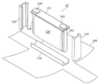
これらの図に示すように、蓄電素子10は、容器100と、容器100の上方に設けられるふた板110と、正極端子200と、負極端子300とを備えている。また、容器100内方には、電極体120と、正極集電体130と、負極集電体140と、側面スペーサ150、160と、底面スペーサ170と、絶縁材180とが配置されている。
As shown in these drawings, the
なお、蓄電素子10の容器100の内部には電解液などの液体が封入されているが、当該液体の図示は省略する。また、蓄電素子10は、非水電解質電池には限定されず、非水電解質電池以外の二次電池であってもよいし、キャパシタであってもよい。
Note that a liquid such as an electrolytic solution is sealed inside the
容器100は、金属からなる矩形筒状で底を備える容器本体であり、金属製のふた板110で当該容器本体の開口が閉塞されている。つまり、容器100は、電極体120等を内部に収容後、ふた板110と溶接等されることにより、内部を密封することができるものとなっている。なお、本実施の形態では、容器100の開口とは反対側の面を容器100の底面と定義する。
The
電極体120は、詳細な図示は省略するが、正極と負極とセパレータとを備え、電気を蓄えることができる部材である。正極は、アルミニウム箔からなる長尺帯状の正極基材の表面に正極活物質層が形成されたものである。負極は、銅箔からなる長尺帯状の負極基材の表面に負極活物質層が形成されたものである。セパレータは、樹脂からなる微多孔性のシートである。そして、電極体120は、負極と正極との間にセパレータが挟み込まれるように層状に配置されたものを全体が長円形状となるように巻き回されて形成されている。
Although detailed illustration is omitted, the
さらに詳しくは、上記正極と上記負極は、上記セパレータを介し、長尺帯状の幅方向に互いにずらして、当該幅方向に沿う巻回軸を中心に長円形状に巻回されている。そして、上記正極及び上記負極は、それぞれのずらす方向の端縁部を活物質の非形成部とすることにより、捲回軸の一端部には、活物質が形成されていない正極基材であるアルミニウム箔が露出し、捲回軸の他端部には、活物質が形成されていない負極基材である銅箔が露出している。また、電極体120の捲回軸方向の両端部には正極集電体130及び負極集電体140が上記捲回軸方向と垂直方向に延びて配置されている。
More specifically, the positive electrode and the negative electrode are wound in an oval shape around the winding axis along the width direction while being shifted from each other in the width direction of the long band via the separator. And the said positive electrode and the said negative electrode are the positive electrode base materials in which the active material is not formed in the one end part of the winding axis | shaft by making the edge part of each shift direction into the non-formation part of an active material The aluminum foil is exposed, and the copper foil, which is a negative electrode base material on which no active material is formed, is exposed at the other end of the winding shaft. Further, a positive electrode
また、電極体120は、正極及び負極とセパレータとが平面で積層されている平面部と、曲面で積層されている曲面部とが形成されている。そして、電極体120は、容器100の底面に対して曲面部が対向するように、容器100に収容される。
In addition, the
ここで、正極活物質としては、LiMPO4、LiMSiO4、LiMBO3(MはFe、Ni、Mn、Co等から選択される1種または2種以上の遷移金属元素)等のポリアニオン化合物、チタン酸リチウム、マンガン酸リチウム等のスピネル化合物、LiMO2(MはFe、Ni、Mn、Co等から選択される1種または2種以上の遷移金属元素)等のリチウム遷移金属酸化物等を用いることができる。 Here, examples of the positive electrode active material include polyanion compounds such as LiMPO 4 , LiMSiO 4 , LiMBO 3 (M is one or more transition metal elements selected from Fe, Ni, Mn, Co, etc.), titanic acid, and the like. Use of spinel compounds such as lithium and lithium manganate, lithium transition metal oxides such as LiMO 2 (M is one or more transition metal elements selected from Fe, Ni, Mn, Co, etc.), etc. it can.
また、負極活物質としては、リチウムイオンを吸蔵放出可能な負極活物質であれば、適宜公知の材料を使用できる。例えば、リチウム金属、リチウム合金(リチウム−ケイ素、リチウム−アルミニウム、リチウム−鉛、リチウム−錫、リチウム−アルミニウム−錫、リチウム−ガリウム、及びウッド合金等のリチウム金属含有合金)の他、リチウムを吸蔵・放出可能な合金、炭素材料(例えば黒鉛、難黒鉛化炭素、易黒鉛化炭素、低温焼成炭素、非晶質カーボン等)、ケイ素酸化物、金属酸化物、リチウム金属酸化物(Li4Ti5O12等)、ポリリン酸化合物などが挙げられる。 Moreover, as a negative electrode active material, if a negative electrode active material which can occlude / release lithium ion, a well-known material can be used suitably. For example, lithium is occluded in addition to lithium metal and lithium alloys (lithium-containing alloys such as lithium-silicon, lithium-aluminum, lithium-lead, lithium-tin, lithium-aluminum-tin, lithium-gallium, and wood alloys). Releasable alloys, carbon materials (eg, graphite, non-graphitizable carbon, graphitizable carbon, low-temperature calcined carbon, amorphous carbon, etc.), silicon oxide, metal oxide, lithium metal oxide (Li 4 Ti 5 O 12 ) and polyphosphoric acid compounds.
なお、同図では、電極体120の形状としては長円形状を示したが、円形状または楕円形状でもよい。
In addition, in the same figure, although the ellipse shape was shown as a shape of the
正極端子200は、電極体120の正極に電気的に接続された電極端子であり、負極端子300は、電極体120の負極に電気的に接続された電極端子である。つまり、正極端子200及び負極端子300は、電極体120に蓄えられている電気を蓄電素子10の外部空間に導出し、また、電極体120に電気を蓄えるために蓄電素子10の内部空間に電気を導入するための金属製の電極端子である。また、正極端子200及び負極端子300は、電極体120の上方に配置されたふた板110に取り付けられている。
The
正極集電体130は、電極体120の正極と容器100の側壁との間に配置され、正極端子200と電極体120の正極とに電気的に接続される導電性と剛性とを備えた部材である。なお、正極集電体130は、電極体120の正極と同様、アルミニウムで形成されている。
The positive electrode
負極集電体140は、電極体120の負極と容器100の側壁との間に配置され、負極端子300と電極体120の負極とに電気的に接続される導電性と剛性とを備えた部材である。なお、負極集電体140は、電極体120の負極と同様、銅で形成されている。
The negative electrode
側面スペーサ150、160及び底面スペーサ170は、電極体120と容器100との間の空間を低減し、電極体120が容器100内で動くことを抑制するように構成されたスペーサである。
The side spacers 150 and 160 and the
具体的には、側面スペーサ150、160は、正極集電体130及び負極集電体140と容器100の側壁との間に配置され、正極集電体130及び負極集電体140に沿って延びる長尺状の絶縁性を有する部材である。例えば、側面スペーサ150、160は、ポリプロピレン(PP)などの樹脂である。つまり、側面スペーサ150、160は、正極集電体130及び負極集電体140と容器100とを絶縁する。また、側面スペーサ150、160は、正極集電体130及び負極集電体140と容器100との間のスペースを埋めることにより、正極集電体130及び負極集電体140を介して電極体120が容器100に対して振動しないように支持する。
Specifically, the
底面スペーサ170は、電極体120と容器100の底面との間に配置され、電極体120の捲回軸方向に沿って延びる長尺状の絶縁性を有する部材である。例えば、底面スペーサ170は、ポリプロピレン(PP)などの樹脂である。より具体的には、底面スペーサ170は、容器100の底面と電極体120の曲面部との間に配置される。つまり、底面スペーサ170は、電極体120と容器100とを絶縁する。また、底面スペーサ170は、電極体120と容器100との間のスペースを埋めることにより、電極体120が容器100に対して振動しないように支持する。底面スペーサ170の詳細な構成の説明については、後述する。
The
絶縁材180は、電極体120と容器100とを絶縁する絶縁材である。具体的には、絶縁材180は、絶縁性を有するシート状の部材であり、底面スペーサ170と電極体120とを覆うように配置される。つまり、絶縁材180は、袋を展開したような形状となっており、底面スペーサ170の下方から、底面スペーサ170と、側面スペーサ150及び160と、正極集電体130及び負極集電体140と、電極体120の側面とを包み込む。これにより、底面スペーサ170と側面スペーサ150及び160とは、絶縁材180と電極体120との間に配置される。
The insulating
このように、絶縁材180は、底面スペーサ170と側面スペーサ150及び160と電極体120とを包み込むように、大きさが調整されて成形されている。なお、絶縁材180は、電極体120の全てを包み込まなくてもよく、電極体120の一部のみを覆うように成形されていることにしてもよい。また、絶縁材180は、袋状に形成できる形状であれば、どのような形状であってもよい。
As described above, the insulating
図3は、本発明の実施の形態に係る底面スペーサ170と電極体120とが絶縁材180で覆われた状態で容器100に挿入されるのを示す図である。
FIG. 3 is a diagram illustrating that the
同図に示すように、絶縁材180は、底面スペーサ170と、側面スペーサ150及び160と、正極集電体130及び負極集電体140と、電極体120とを、底面スペーサ170の下方から包み込むように覆う。そして、絶縁材180で覆われた集合体は、容器100に挿入される。
As shown in the figure, the insulating
次に、底面スペーサ170の詳細な構成について、説明する。
Next, a detailed configuration of the
図4は、本発明の実施の形態に係る蓄電素子10の内部における電極体120と底面スペーサ170との位置関係を示す図である。なお、同図は、正極集電体130、負極集電体140、側面スペーサ150、160、及び絶縁材180は省略して示している。
FIG. 4 is a diagram showing a positional relationship between the
また、図5A及び図5Bは、本発明の実施の形態に係る底面スペーサ170の構成を示す図である。具体的には、図5Aは、底面スペーサ170を斜めから見た外観斜視図であり、図5Bは、図5Aに示された底面スペーサ170を同図の左下側から見た図である。
5A and 5B are diagrams showing the configuration of the
まず、図4に示すように、電極体120には、正極及び負極のそれぞれに活物質が塗工されていない領域である未塗工領域A1が捲回軸方向の両端に設けられており、正極及び負極に活物質が塗工されている領域である塗工領域A2が、未塗工領域A1の間の電極体120の捲回軸方向の中央に設けられている。
First, as shown in FIG. 4, the
そして、底面スペーサ170は、電極体120の未塗工領域A1に対向する2つの第一部分171と、電極体120の塗工領域A2に対向する第二部分172とを有している。底面スペーサ170は、電極体120の捲回軸方向に直交する平面における第一部分171の断面形状と、当該平面における第二部分172の断面形状とが異なる。
The
具体的には、図5A及び図5Bに示すように、第一部分171の厚みの方が第二部分172の厚みよりも厚いように形成されている。つまり、底面スペーサ170の第一部分171と電極体120の未塗工領域A1との隙間よりも、底面スペーサ170の第二部分172と電極体120の塗工領域A2との隙間の方が大きくなるように形成されている。
Specifically, as shown in FIGS. 5A and 5B, the
また、それぞれの第一部分171は、内面部171aと、2つの側面部171bと、外面部171cとを有している。
Each
内面部171aは、電極体120に対向する面であり、電極体120の外面に沿った形状を有している。つまり、底面スペーサ170は、第一部分171の電極体120側の形状が、電極体120の未塗工領域A1の外面に沿う形状である。具体的には、内面部171aは、凹んだ曲面形状を有している。
The
側面部171bは、内面部171aの両側に配置される平面形状の面である。つまり、底面スペーサ170は、第一部分171の側面形状が容器100の内面の側面に沿う形状である。
The
外面部171cは、絶縁材180に対向して2つの側面部171bの間に配置される平面形状の面である。つまり、底面スペーサ170は、第一部分171の底面形状が容器100の内面の底面に沿う形状である。
The
そして、2つの側面部171bのうち少なくとも1つの側面部171bと内面部171aとは、曲面で接続されている。つまり、図5Bに示すように、2つの側面部171bと内面部171aとは、曲面R1及び曲面R2で接続されている。なお、曲面R1及び曲面R2は曲面であればよく、その形状は限定されないが、例えば、半径が1〜2mmの円弧状の断面形状を有する曲面である。
At least one
また、2つの側面部171bのうち少なくとも1つの側面部171bと外面部171cとは、曲面で接続されている。つまり、図5Bに示すように、2つの側面部171bと外面部171cとは、曲面R3及び曲面R4で接続されている。なお、曲面R3及び曲面R4は曲面であればよく、その形状は限定されないが、例えば、半径が1〜3mmの円弧状の断面形状を有する曲面である。
Moreover, at least one
また、第一部分171と同様に、第二部分172は、内面部172aと、2つの側面部172bと、外面部172cとを有している。
Similarly to the
内面部172aは、電極体120に対向する面であり、電極体120の外面に沿った形状を有している。つまり、底面スペーサ170は、第二部分172の電極体120側の形状が、電極体120の塗工領域A2の外面に沿う形状である。具体的には、内面部172aは、凹んだ曲面形状を有している。
The
側面部172bは、内面部172aの両側に配置される面である。つまり、底面スペーサ170は、第二部分172の側面形状が容器100の内面の側面に沿う形状である。
The
外面部172cは、絶縁材180に対向して2つの側面部172bの間に配置される面である。つまり、底面スペーサ170は、第二部分172の底面形状が容器100の内面の底面に沿う形状である。
The
そして、第一部分171と同様に、2つの側面部172bのうち少なくとも1つの側面部172bと内面部172aとは、曲面で接続されている。ここでは、2つの側面部172bの双方と内面部172aとは、曲面で接続されている。なお、当該曲面の形状は限定されないが、例えば、半径が1〜2mmの円弧状の断面形状を有する曲面である。
And like the
また、第一部分171と同様に、2つの側面部172bのうち少なくとも1つの側面部172bと外面部172cとは、曲面で接続されている。ここでは、2つの側面部172bの双方と外面部172cとは、曲面で接続されている。なお、当該曲面の形状は限定されないが、例えば、半径が1〜3mmの円弧状の断面形状を有する曲面である。
Similarly to the
これらのように、底面スペーサ170は、底面スペーサ170の短手方向の端部に、電極体120の側方に沿って底面スペーサ170の長手方向に延びるように配置されている側部の先端部を形成する面が曲面となるように形成されている。
As described above, the
なお、第一部分171や第二部分172と同様に、側面スペーサ150及び160の電極体120に対向する内面部と、当該内面部の両側に配置される2つの側面部とは、曲面で接続されていることにしてもよい。また、側面スペーサ150及び160の2つの側面部と、絶縁材180に対向して2つの側面部の間に配置される外面部とは、曲面で接続されていることにしてもよい。
Similar to the
以上のように、本発明の実施の形態に係る蓄電素子10によれば、底面スペーサ170が絶縁材180と電極体120との間に配置された構成を有している。つまり、容器100の底面に沿って配置される、比較的大きな体積をもつ底面スペーサ170は、絶縁材180と電極体120との間に挟まれた状態で、電極体120に固定される。そして、底面スペーサ170が、絶縁材180と電極体120との間で固定された状態で(すなわち、電極体120と底面スペーサ170との相対位置が絶縁材180によって固定された状態で)容器100に挿入されることで、蓄電素子10が構成される。このように、電極体120よりも先に容器100に挿入され、電極体120により容器100の底面に向けて押し込まれる底面スペーサ170が、絶縁材180で電極体120に固定されて容器100に挿入されるため、容器100内での底面スペーサ170の位置ずれを低減しつつ、底面スペーサ170を円滑に容器100に挿入することができる。
As described above, according to
また、蓄電素子10は、絶縁材180が電極体120と底面スペーサ170とを覆うように配置された構成を有している。つまり、絶縁材180が電極体120と底面スペーサ170とを包み込むようにして、電極体120と底面スペーサ170とを固定している。このため、底面スペーサ170が絶縁材180で覆われて電極体120に固定され容器100に挿入されるため、容器100内での底面スペーサ170の位置ずれを低減しつつ、底面スペーサ170を円滑に容器100に挿入することができる。
In addition, the
また、絶縁材180はシート状の部材であるため、容易に底面スペーサ170を包み込んで電極体120に固定することができる。
Further, since the insulating
また、底面スペーサ170の少なくとも1つの側面部と内面部とは、曲面で接続されている。つまり、底面スペーサ170は、電極体120に固定される際に電極体120に接触する先端部分が丸くなっている構成を有する。これにより、底面スペーサ170が電極体120に固定される際に、底面スペーサ170の先端で電極体120を損傷させることを防止することができる。
Further, at least one side surface portion and the inner surface portion of the
また、底面スペーサ170の少なくとも1つの側面部と外面部とは、曲面で接続されている。つまり、底面スペーサ170は、絶縁材180に接触する角部が丸くなっている構成を有する。これにより、振動などで底面スペーサ170と絶縁材180とが擦れた場合でも、底面スペーサ170の角部で絶縁材180を損傷させることを防止することができる。
Further, at least one side surface portion of the
また、底面スペーサ170は絶縁性の部材であるため、例えば、底面スペーサ170が絶縁材180で包み込まれて電極体120に固定される際などに、絶縁材180が損傷したような場合でも、電極体120と容器100との間の絶縁性を確保することができる。
Further, since the
また、底面スペーサ170の活物質の未塗工領域A1に対向する第一部分171の厚みの方が、底面スペーサ170の活物質の塗工領域A2に対向する第二部分172の厚みよりも厚い。ここで、未塗工領域A1は、圧迫されても蓄電素子10の性能低下を引き起こしにくい領域である。この蓄電素子10では、その耐振動性を高めるために未塗工領域A1に対向する底面スペーサ170の第一部分171の厚みを第二部分172よりも厚くして未塗工領域A1を圧迫しているため、蓄電素子10の性能をあまり低下させずに耐振動性を高めることができる。また、塗工領域A2は、充放電を繰り返すことにより膨らみやすい領域であり、過剰に圧迫されると蓄電素子10の性能が低下しやすい領域である。このため、底面スペーサ170の第二部分172の厚みを第一部分171の厚みよりも薄くすることにより、電極体120の膨らみを許容できる空間を設けることができ、電極体120が膨張しても蓄電素子10の性能を低下することを防ぐことができる。
Further, the thickness of the
また、電極体120の塗工領域A2に対向する位置との隙間(クリアランス)が、電極体120の未塗工領域A1に対向する位置とのクリアランスよりも大きくなるように底面スペーサ170が形成されている。このため、電極体120は充放電を繰り返すことによりその塗工領域A2が膨張しても、塗工領域A2に対向する位置のクリアランスが大きいため、電極体120の塗工領域A2の膨張を許容できる。また、電極体120は、圧迫されることによる蓄電素子10の性能低下が起こりにくい未塗工領域A1のクリアランスが小さいため、蓄電素子10の性能低下を起こさないような状態で耐振動性を向上させることができる。
Further, the
また、底面スペーサ170の第一部分171の電極体120側の形状が電極体120に沿う形状であるため、第一部分171に対応する位置における隙間(クリアランス)を最小とすることができる。このため、底面スペーサ170は、第一部分171において耐振動性をより向上させることができる。
In addition, since the shape of the
次に、蓄電素子10の製造方法について、説明する。
Next, the manufacturing method of the
図6は、本発明の実施の形態に係る蓄電素子10の製造方法の一例を示すフローチャートである。
FIG. 6 is a flowchart showing an example of a method for manufacturing
図7A〜図7Cは、本発明の実施の形態に係る蓄電素子10の製造方法を説明するための図である。なお、同図は、ふた板110、正極集電体130、負極集電体140及び側面スペーサ150、160は省略して示している。
7A to 7C are diagrams for explaining a method of manufacturing
まず、図6に示すように、底面スペーサ170の配置工程として、底面スペーサ170を、絶縁材180と電極体120との間に配置する(S102)。
First, as shown in FIG. 6, as a step of arranging the
具体的には、図7Aに示すように、底面スペーサ170を絶縁材180上に載置し、貼り付ける。つまり、絶縁材180は、接着剤や接着テープなどを用いて、底面スペーサ170に接着されて固定される。または、代替的に、絶縁材180は、超音波溶着などを用いて、底面スペーサ170に溶着されて固定されてもよい。これにより、容器100内での底面スペーサ170の位置ずれを効果的に低減することができる。また、絶縁材180上の底面スペーサ170の側方に、電極体120を底部が底面スペーサ170に対向するように横置きに載置する。
Specifically, as shown in FIG. 7A, the
そして、図7Bに示すように、絶縁材180を電極体120に巻きつけるように底面スペーサ170とともに持ち上げていく。この際に、同図に示すように底面スペーサ170の先端部が電極体120に当接するが、底面スペーサ170の先端部は丸く成形されているため、電極体120が損傷するのを防ぐことができる。
Then, as shown in FIG. 7B, the insulating
そして、図7Cに示すように、絶縁材180で底面スペーサ170と電極体120とを覆うように、絶縁材180を電極体120に巻きつける。このようにして、底面スペーサ170を絶縁材180と電極体120との間に配置する。
Then, as illustrated in FIG. 7C, the insulating
以上のように、当該配置工程では、絶縁材180の上に、底面スペーサ170を載置するとともに、長尺帯状の正極および負極を巻き回されて巻回軸を中心に長円形状に巻回された電極体120を横置きにし、絶縁材180を電極体120に巻きつけることで底面スペーサ170を絶縁材180と電極体120との間に配置する。これにより、製造効率を向上することができる。
As described above, in the arrangement step, the
そして、図6に戻り、底面スペーサ170の挿入工程として、底面スペーサ170を、絶縁材180と電極体120とともに容器100内に挿入する(S104)。
Returning to FIG. 6, as a step of inserting the
具体的には、図7Cに示すように、容器100を開口が水平方向に向くように横置きに配置する。そして、絶縁材180で底面スペーサ170と電極体120とを包み込んだ状態の集合体を、容器100の開口から水平方向に容器100内に挿入する。
Specifically, as shown in FIG. 7C, the
このように、容器100を横向きに配置することで、容器100を強い力で保持し易くなり、底面スペーサ170と電極体120とを絶縁材180で包み込んだ集合体を、容器100に挿入し易くなる。
In this way, by arranging the
以上のように、本発明の実施の形態に係る蓄電素子10の製造方法によれば、底面スペーサ170は、絶縁材180と電極体120との間に配置される。つまり、底面スペーサ170は、絶縁材180と電極体120との間に挟まれた状態で、電極体120に固定される。そして、底面スペーサ170が絶縁材180と電極体120との間で固定された状態で容器100に挿入されることで、蓄電素子10が構成される。このように、底面スペーサ170が絶縁材180で電極体120に固定されて容器100に挿入されるため、容器100内での底面スペーサ170の位置ずれを低減しつつ、底面スペーサ170を円滑に容器100に挿入することができる。
As described above, according to the method for manufacturing
また、絶縁材180が電極体120と底面スペーサ170とを覆うように、底面スペーサ170を絶縁材180と電極体120との間に配置する。つまり、絶縁材180が電極体120と底面スペーサ170とを包み込むようにして、電極体120と底面スペーサ170とを固定する。このため、底面スペーサ170が絶縁材180で覆われて電極体120に固定され容器100に挿入されるため、容器100内での底面スペーサ170の位置ずれを低減しつつ、底面スペーサ170を円滑に容器に挿入することができる。
In addition, the
(変形例1)
次に、本実施の形態の変形例1について説明する。上記実施の形態では、絶縁材180はシート状の部材であることとした。しかし、本変形例1では、絶縁材は袋状の部材である。
(Modification 1)
Next, Modification 1 of the present embodiment will be described. In the above embodiment, the insulating
図8は、本発明の実施の形態の変形例1に係る蓄電素子11の構成を示す図である。なお、同図では、容器100は省略して、容器100の内部の構成について示している。
FIG. 8 is a diagram showing a configuration of a
同図に示すように、蓄電素子11は、上部が開口した袋状の絶縁材181を備えている。ここで、絶縁材181は、絶縁性のシートを袋状に加工することで成形された絶縁材である。
As shown in the figure, the
そして、絶縁材181は、底面スペーサ170と電極体120とを覆うように配置される。つまり、電極体120と、正極集電体130と、負極集電体140と、側面スペーサ150及び160と、底面スペーサ170とが、絶縁材181の内方に収容されて、容器100内に挿入される。
The insulating
ここで、絶縁材181は、電極体120と、正極集電体130と、負極集電体140と、側面スペーサ150及び160と、底面スペーサ170とを内方に収容できるように、大きさが調整されて成形されている。なお、絶縁材181は、電極体120の全てを内方に収容できなくともよく、電極体120の下部の一部のみを覆うように成形されていることにしてもよい。
Here, the insulating
以上のように、本発明の実施の形態の変形例1に係る蓄電素子12によれば、袋状の絶縁材181が電極体120とスペーサ(側面スペーサ150及び160と底面スペーサ170)とを覆うように配置された構成を有している。つまり、絶縁材181が電極体120と当該スペーサとを包み込むようにして、電極体120と当該スペーサとを固定している。このため、当該スペーサが絶縁材181で覆われて電極体120に固定され容器100に挿入されるため、容器100内での当該スペーサの位置ずれを低減しつつ、当該スペーサを円滑に容器100に挿入することができる。
As described above, according to
(変形例2)
次に、本実施の形態の変形例2について説明する。上記実施の形態では、絶縁材180は底面スペーサ170と側面スペーサ150、160の双方を覆うように配置されることとした。しかし、本変形例2では、絶縁材は、底面スペーサ170および/または側面スペーサ150、160を覆うように配置される。
(Modification 2)
Next, a second modification of the present embodiment will be described. In the above embodiment, the insulating
図9〜図11は、本発明の実施の形態の変形例2に係る蓄電素子の構成を示す図である。なお、図9及び図10では、容器100は省略して、容器100の内部の構成について示している。
9-11 is a figure which shows the structure of the electrical storage element which concerns on the modification 2 of embodiment of this invention. In FIGS. 9 and 10, the
図9に示すように、蓄電素子12は、長方形状のシート状の絶縁材182を備えている。そして、絶縁材182は、底面スペーサ170と電極体120とを覆うように配置される。つまり、電極体120と、正極集電体130と、負極集電体140と、側面スペーサ150及び160と、底面スペーサ170とが、電極体120の下方から絶縁材182に包み込まれるように覆われる。
As shown in FIG. 9, the
ここで、絶縁材182は、電極体120と、正極集電体130と、負極集電体140と、側面スペーサ150及び160と、底面スペーサ170とを包み込むように、大きさが調整されて成形されている。例えば、側面スペーサ150及び160を電極体120に組み付けた後、底面スペーサ170に接着または超音波溶着された絶縁材182により電極体120と側面スペーサ150及び160とを包み込み、そして絶縁材182を側面スペーサ150及び160に熱溶着する。なお、絶縁材182は、電極体120の全てを包み込まなくてもよく、電極体120の一部のみを覆うように成形されていることにしてもよい。
Here, the size of the insulating
また、図10に示すように、蓄電素子13は、長方形状のシート状の絶縁材183を備えている。そして、絶縁材183は、側面スペーサ150及び160と電極体120とを覆うように配置される。つまり、電極体120と、正極集電体130と、負極集電体140と、側面スペーサ150及び160と、底面スペーサ170とが、電極体120の側方から絶縁材183に包み込まれるように覆われる。
As illustrated in FIG. 10, the
そして、図11に示すように、粘着テープ184などにより絶縁材183の端部が固定されて、容器100内に挿入される。
And as shown in FIG. 11, the edge part of the insulating
ここで、絶縁材183は、電極体120と、正極集電体130と、負極集電体140と、側面スペーサ150及び160と、底面スペーサ170とを包み込むように、大きさが調整されて成形されている。なお、絶縁材183は、電極体120の全てを包み込まなくてもよく、電極体120の一部のみを覆うように成形されていることにしてもよい。
Here, the size of the insulating
また、蓄電素子13の構成の場合、電極体120や絶縁材183の損傷を防止するために、底面スペーサ170と同様に、側面スペーサ150及び160の電極体120または絶縁材183と接触する角部は、曲面形状であるのが好ましい。つまり、側面スペーサ150及び160の電極体120に対向する内面部と、当該内面部の両側に配置される2つの側面部とは、曲面で接続されているのが好ましい。また、側面スペーサ150及び160の2つの側面部と、絶縁材183に対向して2つの側面部の間に配置される外面部とは、曲面で接続されているのが好ましい。
Further, in the case of the configuration of the
以上のように、本発明の実施の形態の変形例2に係る蓄電素子12、13によれば、絶縁材182、183が電極体120とスペーサ(側面スペーサ150及び160と底面スペーサ170)とを下方または側方から覆うように配置された構成を有している。つまり、絶縁材182、183が電極体120と当該スペーサとを下方または側方から包み込むようにして、電極体120と当該スペーサとを固定している。このため、当該スペーサが下方または側方から絶縁材182、183で覆われて電極体120に固定され容器100に挿入されるため、容器100内での当該スペーサの位置ずれを低減しつつ、当該スペーサを円滑に容器100に挿入することができる。
As described above, according to the
(変形例3)
次に、本実施の形態の変形例3について説明する。上記実施の形態では、底面スペーサ170は、2つの第一部分171と、当該2つの第一部分171に挟まれた第二部分172とで構成されることとした。しかし、本変形例3では、底面スペーサ170は、さらに第三部分を有する。
(Modification 3)
Next, a third modification of the present embodiment will be described. In the above embodiment, the
図12は、本発明の実施の形態の変形例3に係る蓄電素子が備える底面スペーサ170Aの構成を示す図である。
FIG. 12 is a diagram showing a configuration of a
同図に示すように、底面スペーサ170Aは、長手方向の両端に配置される2つの第一部分171と、2つの第一部分171のそれぞれに接続される2つの第二部分173とを有している。そして、底面スペーサ170Aは、2つの第二部分173の間に第三部分174を有している。
As shown in the figure, the
ここで、第三部分174は、2つの第二部分173よりも厚みが薄い平板状の部位である。つまり、底面スペーサ170Aは、上記実施の形態における底面スペーサ170の中央部分の厚みが薄くなったような形状を有する。
Here, the
なお、第三部分174の形状は平板状に限定されず、曲面形状などどのような形状を有していてもよい。また、第一部分171と第二部分173と第三部分174とは、同じ材質で構成されていてもよいし、異なる材質で構成されていてもよい。
Note that the shape of the
以上のように、本発明の実施の形態の変形例3に係る蓄電素子が備える底面スペーサ170Aによれば、2つの第二部分173の間に第二部分173よりも厚みが薄い第三部分174を有する。つまり、底面スペーサ170Aは、第一部分171と第二部分173とで電極体120を支持することができるため、電極体120の支持に使用されない第三部分174の厚みを薄くすることで、部品材料の低減によるコスト低減を図ることができる。
As described above, according to the
(変形例4)
次に、本実施の形態の変形例4について説明する。上記実施の形態及びその変形例では、底面スペーサの第一部分の側面部及び外面部と、第二部分の側面部及び外面部とは平面形状を有していることとした。しかし、本変形例4では、底面スペーサの側面部及び外面部は曲面形状を有する。
(Modification 4)
Next, Modification 4 of the present embodiment will be described. In the said embodiment and its modification, suppose that the side part and outer surface part of the 1st part of a bottom surface spacer and the side part and outer surface part of a 2nd part had planar shape. However, in the fourth modification, the side surface portion and the outer surface portion of the bottom spacer have a curved shape.
図13A〜図13Cは、本発明の実施の形態の変形例4に係る蓄電素子が備える底面スペーサ170Bを説明するための図である。具体的には、図13Aは、図5Bの底面スペーサ170に対応する図であり、図13B及び図13Cは、図7A及び図7Bの蓄電素子10の製造方法に対応する図である。
FIGS. 13A to 13C are diagrams for explaining a
図13Aに示すように、底面スペーサ170Bは、第一部分175と第二部分176とを備えている。そして、第一部分175は、上面に内面部175aと、側面に2つの側面部175bと、底面に外面部175cとを備えている。同様に、第二部分176は、上面に内面部176aと、側面に2つの側面部176bと、底面に外面部176cとを備えている。
As illustrated in FIG. 13A, the
ここで、これらの2つの側面部175b、外面部175c、2つの側面部176b、外面部176cは、曲面形状を有している。つまり、側面部175bは、内面部175aの両側に配置される曲面形状の面であり、外面部175cは、絶縁材180に対向して2つの側面部175bの間に配置される曲面形状の面である。また、側面部176bは、内面部176aの両側に配置される曲面形状の面であり、外面部176cは、絶縁材180に対向して2つの側面部176bの間に配置される曲面形状の面である。
Here, the two
そして、このような底面スペーサ170Bを有する蓄電素子の製造過程においては、図13Bに示すように、まず、底面スペーサ170Bを絶縁材180上の電極体120の側方に載置し、図13Cに示すように、絶縁材180を電極体120に巻きつけるように底面スペーサ170Bとともに持ち上げ、絶縁材180を電極体120に巻きつけていく。
Then, in the manufacturing process of the electric storage element having such a
この際、底面スペーサ170Bは、側面部及び外面部が曲面で形成されているため、絶縁材180をスムーズに折り曲げることができる。そして、底面スペーサ170Bは、絶縁材180と電極体120とともに、容器100内に挿入される。
At this time, since the
なお、底面スペーサ170Bの側面部及び外面部は、全部が曲面形状を有していることには限られず、曲面形状を有しているのは、2つの側面部175b、外面部175c、2つの側面部176b、外面部176cのうちの一部であってもよい。
Note that the side surface portion and the outer surface portion of the
(変形例5)
次に、本実施の形態の変形例5について説明する。上記実施の形態及びその変形例では、側面スペーサと底面スペーサとは別体であった。しかし、本変形例5では、スペーサが、側面スペーサとして機能する側面部と、底面スペーサとして機能する底面部とを有する。図14は、本発明の実施の形態の変形例5に係る蓄電素子が備えるスペーサ165を説明するための図である。
(Modification 5)
Next, Modification 5 of the present embodiment will be described. In the said embodiment and its modification, the side surface spacer and the bottom surface spacer were separate bodies. However, in the fifth modification, the spacer has a side part that functions as a side spacer and a bottom part that functions as a bottom spacer. FIG. 14 is a diagram for explaining a
図14に示すように、変形例5に係る蓄電素子が備えるスペーサ165は、側面スペーサとして機能する側面部165aと、底面スペーサとして機能する底面部165bとを有する。この蓄電素子のスペーサ165以外の構成要素は、図9に示した蓄電素子12に含まれる構成要素と類似するため、詳細な説明は省略する。
As illustrated in FIG. 14, the
側面部165aは、容器の側壁に沿って配置される。底面部165bは、容器の底面に沿って配置される。側面部165aは、底面部165bとは略直交する方向に延びている。このスペーサ165は、図9に示す電極体120に組み付けられた後、絶縁材182によりその底面部165bが電極体120とともに包み込まれる。
The
以上、本発明の実施の形態及びその変形例に係る蓄電素子について説明したが、本発明は、この実施の形態及びその変形例に限定されるものではない。 The power storage device according to the embodiment of the present invention and the modification thereof has been described above, but the present invention is not limited to this embodiment and the modification thereof.
つまり、今回開示された実施の形態及びその変形例は全ての点で例示であって制限的なものではないと考えられるべきである。本発明の範囲は上記した説明ではなくて特許請求の範囲によって示され、特許請求の範囲と均等の意味及び範囲内での全ての変更が含まれることが意図される。また、上記実施の形態及び上記変形例を任意に組み合わせて構築される形態も、本発明の範囲内に含まれる。 In other words, it should be considered that the embodiment and its modification disclosed this time are illustrative and not restrictive in all respects. The scope of the present invention is defined by the terms of the claims, rather than the description above, and is intended to include any modifications within the scope and meaning equivalent to the terms of the claims. Moreover, the form constructed | assembled combining the said embodiment and the said modification arbitrarily is also contained in the scope of the present invention.
例えば、上記実施の形態では、底面スペーサ170は、第一部分171と、第一部分171よりも厚みが薄い第二部分172とを有していることとした。しかし、底面スペーサ170は、第一部分171と、第一部分171よりも硬度が低い第二部分172とを有していることにしてもよい。また、底面スペーサ170は、第二部分172を有しておらず、第一部分171のみ有していることにしてもよい。これらの構成によっても、底面スペーサ170は、電極体120の膨張を許容しつつ、電極体120を支持することができる。
For example, in the above embodiment, the
本発明は、容器内でのスペーサの位置ずれを低減しつつ、当該スペーサを円滑に容器に挿入することができる蓄電素子等に適用できる。 INDUSTRIAL APPLICABILITY The present invention can be applied to a power storage element that can smoothly insert a spacer into the container while reducing the displacement of the spacer in the container.
10、11、12、13 蓄電素子
100 容器
110 ふた板
120 電極体
130 正極集電体
140 負極集電体
150、160 側面スペーサ
165 スペーサ
165a 側面部
165b 底面部
170、170A 底面スペーサ
171 第一部分
171a 内面部
171b 側面部
171c 外面部
172、173 第二部分
172a 内面部
172b 側面部
172c 外面部
174 第三部分
180、181、182、183 絶縁材
184 粘着テープ
200 正極端子
300 負極端子
10, 11, 12, 13
Claims (13)
前記容器内に配置され、前記電極体と前記容器とを絶縁する絶縁材と、
前記容器内に配置されるスペーサとを備え、
前記絶縁材は、前記スペーサと前記電極体とを覆うシート状の部材であり、
前記スペーサは、前記絶縁材と前記電極体との間に配置される
蓄電素子。 Electrode having a positive electrode and the negative electrode, and a storage element including a container and a cover plate having an opening closed by the electrode terminals attached to the container body and the container body that houses the electrode body,
An insulating material disposed in the container and insulating the electrode body and the container;
A spacer disposed in the container,
The insulating material is a sheet-like member that covers the spacer and the electrode body,
The spacer is disposed between the insulating material and the electrode body.
請求項1に記載の蓄電素子。 The power storage device according to claim 1, wherein the spacer is configured to reduce a space between the electrode body and the container and to prevent the electrode body from moving in the container.
請求項1または2に記載の蓄電素子。 The insulating material, the electric storage device according to claim 1 or 2 is bonded or welded to the spacer.
前記2つの側面部のうち少なくとも1つの側面部と前記内面部とは、曲面で接続される
請求項1〜3のいずれか1項に記載の蓄電素子。 The spacer has an inner surface facing the electrode body and two side surfaces disposed on both sides of the inner surface.
At least one of the side surface portion and the inner surface portion, the electric storage device according to any one of claims 1 to 3 connected by a curved surface of said two side portions.
前記2つの側面部のうち少なくとも1つの側面部と前記外面部とは、曲面で接続される
請求項1〜4のいずれか1項に記載の蓄電素子。 The spacer includes an inner surface facing the electrode body, two side surfaces disposed on both sides of the inner surface, and an outer surface disposed between the two side surfaces facing the insulating material. Have
At least one of the side surface portion and the outer surface, the electric storage device according to any one of claims 1 to 4 connected by a curved surface of said two side portions.
請求項1〜5のいずれか1項に記載の蓄電素子。 The spacer, the electric storage device according to any one of claims 1 to 5, which is a member of the insulative.
前記スペーサは、前記未塗工領域に対向する第一部分と、前記塗工領域に対向する第二部分とを有し、
前記第一部分の厚みの方が前記第二部分の厚みよりも厚い
請求項1〜6のいずれか1項に記載の蓄電素子。 The electrode body has a coated region in which an active material is coated on the surfaces of the positive electrode and the negative electrode, and an uncoated region in which an active material is not coated on the surfaces of the positive electrode and the negative electrode. ,
The spacer has a first portion facing the uncoated region, and a second portion facing the coated region,
The electric storage element according to any one of the thick claims 1-6 than the thickness of said second portion towards said first portion of the thickness.
請求項7に記載の蓄電素子。 Than the gap between the uncoated region of the electrode body and the first portion of the spacer, according to claim 7 the larger the gap between the coating area of the electrode body and the second portion of the spacer Power storage element.
請求項7または8に記載の蓄電素子。 The electricity storage device according to claim 7 or 8 , wherein the spacer has a shape of the first portion on the electrode body side along an outer surface of the electrode body.
請求項7〜9のいずれか1項に記載の蓄電素子。 The spacer has two first portions disposed at both ends in the longitudinal direction and two second portions connected to the two first portions, respectively, and between the two second portions. the electric storage element according to any one of claims 7-9 having the two third portions thinner than the second portion.
前記スペーサを、前記スペーサと前記電極体とを覆うシート状の部材である前記絶縁材と前記電極体との間に配置する配置工程と、
前記スペーサを、前記絶縁材と前記電極体とともに前記容器内に挿入する挿入工程と
を含む蓄電素子の製造方法。 Electrode having a positive electrode and the negative electrode, wherein the container body that houses the electrode body container having a cover plate closed by the electrode terminal is attached to an opening of the container body, disposed in said container and the electrode body insulating material which insulates the container, and a method for manufacturing a power storage device having a space Sa disposed in said container,
An arrangement step of arranging the spacer between the insulating material and the electrode body, which is a sheet-like member covering the spacer and the electrode body ;
The manufacturing method of an electrical storage element including the insertion process which inserts the said spacer in the said container with the said insulating material and the said electrode body.
請求項11に記載の蓄電素子の製造方法。 The method for manufacturing a power storage element according to claim 11 , wherein, in the arranging step, the spacer is arranged between the insulating material and the electrode body so as to cover the spacer and the electrode body with the insulating material.
請求項12に記載の蓄電素子の製造方法。 In the arranging step, the spacer is placed on the insulating material, and the positive electrode and the negative electrode having a long strip shape are wound, and the electrode is wound in an oval shape around a winding axis. The method for manufacturing a power storage element according to claim 12 , wherein the spacer is disposed between the insulating material and the electrode body by placing the body horizontally and winding the insulating material around the electrode body.
Priority Applications (8)
| Application Number | Priority Date | Filing Date | Title |
|---|---|---|---|
| JP2013004871A JP6003662B2 (en) | 2012-02-15 | 2013-01-15 | Power storage device and method for manufacturing power storage device |
| CN201310041344.2A CN103258983B (en) | 2012-02-15 | 2013-02-01 | The manufacture method of charge storage element and charge storage element |
| CN201710478121.0A CN107256801B (en) | 2012-02-15 | 2013-02-01 | Charge storage element |
| KR1020130013917A KR102045886B1 (en) | 2012-02-15 | 2013-02-07 | Electric storage device and manufacturing the same |
| US13/765,405 US9214652B2 (en) | 2012-02-15 | 2013-02-12 | Electric storage element and method for manufacturing electric storage element |
| DE102013202310.3A DE102013202310B4 (en) | 2012-02-15 | 2013-02-13 | Electrical storage element and method for producing the electrical storage element |
| DE202013012271.4U DE202013012271U1 (en) | 2012-02-15 | 2013-02-13 | Electric storage element |
| US14/850,706 US10074831B2 (en) | 2012-02-15 | 2015-09-10 | Electric storage element and method for manufacturing electric storage element |
Applications Claiming Priority (3)
| Application Number | Priority Date | Filing Date | Title |
|---|---|---|---|
| JP2012030821 | 2012-02-15 | ||
| JP2012030821 | 2012-02-15 | ||
| JP2013004871A JP6003662B2 (en) | 2012-02-15 | 2013-01-15 | Power storage device and method for manufacturing power storage device |
Related Child Applications (1)
| Application Number | Title | Priority Date | Filing Date |
|---|---|---|---|
| JP2016175963A Division JP6237849B2 (en) | 2012-02-15 | 2016-09-08 | Power storage device and method for manufacturing power storage device |
Publications (3)
| Publication Number | Publication Date |
|---|---|
| JP2013191544A JP2013191544A (en) | 2013-09-26 |
| JP2013191544A5 JP2013191544A5 (en) | 2016-04-14 |
| JP6003662B2 true JP6003662B2 (en) | 2016-10-05 |
Family
ID=48915386
Family Applications (1)
| Application Number | Title | Priority Date | Filing Date |
|---|---|---|---|
| JP2013004871A Active JP6003662B2 (en) | 2012-02-15 | 2013-01-15 | Power storage device and method for manufacturing power storage device |
Country Status (5)
| Country | Link |
|---|---|
| US (2) | US9214652B2 (en) |
| JP (1) | JP6003662B2 (en) |
| KR (1) | KR102045886B1 (en) |
| CN (2) | CN107256801B (en) |
| DE (2) | DE202013012271U1 (en) |
Families Citing this family (33)
| Publication number | Priority date | Publication date | Assignee | Title |
|---|---|---|---|---|
| JP6232848B2 (en) * | 2012-09-26 | 2017-11-22 | 株式会社Gsユアサ | Electricity storage element |
| JP2015060712A (en) * | 2013-09-18 | 2015-03-30 | 株式会社東芝 | Secondary battery |
| JP6287186B2 (en) * | 2013-12-26 | 2018-03-07 | 三洋電機株式会社 | Nonaqueous electrolyte secondary battery |
| JP2015170414A (en) * | 2014-03-05 | 2015-09-28 | 株式会社Gsユアサ | Power storage element |
| KR102257678B1 (en) * | 2014-03-28 | 2021-05-28 | 삼성에스디아이 주식회사 | Secondary battery |
| KR102211526B1 (en) * | 2014-04-23 | 2021-02-02 | 삼성에스디아이 주식회사 | Rechargeable battery |
| KR101690367B1 (en) * | 2014-05-21 | 2016-12-27 | 주식회사 엘지화학 | Secondary Battery |
| KR102238623B1 (en) * | 2014-10-15 | 2021-04-08 | 에스케이이노베이션 주식회사 | Jelly roll for use in a secondary battery |
| FR3027457B1 (en) * | 2014-10-17 | 2016-10-28 | Commissariat Energie Atomique | LIMNXCO1-XBO3 FORMULA ELECTRODE MATERIAL AND PROCESS FOR PREPARING THE SAME |
| USD804418S1 (en) * | 2015-07-14 | 2017-12-05 | Gs Yuasa International Ltd. | Rechargeable battery |
| WO2017047787A1 (en) * | 2015-09-18 | 2017-03-23 | リチウム エナジー アンド パワー ゲゼルシャフト ミット ベシュレンクテル ハフッング ウント コンパニー コマンディトゲゼルシャフト | Power storage element and method for manufacturing power storage element |
| JP2017059507A (en) * | 2015-09-18 | 2017-03-23 | リチウム エナジー アンド パワー ゲゼルシャフト ミット ベシュレンクテル ハフッング ウント コンパニー コマンディトゲゼルシャフトLithium Energy and Power GmbH & Co. KG | Power storage device |
| JP2017157342A (en) * | 2016-02-29 | 2017-09-07 | リチウム エナジー アンド パワー ゲゼルシャフト ミット ベシュレンクテル ハフッング ウント コンパニー コマンディトゲゼルシャフトLithium Energy and Power GmbH & Co. KG | Power storage element |
| JP6743417B2 (en) * | 2016-02-29 | 2020-08-19 | 株式会社Gsユアサ | Storage element |
| JP2017157352A (en) * | 2016-02-29 | 2017-09-07 | リチウム エナジー アンド パワー ゲゼルシャフト ミット ベシュレンクテル ハフッング ウント コンパニー コマンディトゲゼルシャフトLithium Energy and Power GmbH & Co. KG | Manufacturing method of power storage element, and power storage element |
| CN105633310B (en) * | 2016-03-28 | 2018-11-20 | 宁德时代新能源科技股份有限公司 | Secondary battery top cover assembly, secondary battery containing same and assembling method |
| US10763465B2 (en) | 2016-03-28 | 2020-09-01 | Contemporary Amperex Technology Co., Limited | Secondary battery head cover assembly, secondary battery including the same and assembling method thereof |
| US10700314B2 (en) | 2016-03-28 | 2020-06-30 | Contemporary Amperex Technolog Co., Limited | Secondary battery head cover assembly, secondary battery including the same and assembling method thereof |
| US11011798B2 (en) | 2016-06-24 | 2021-05-18 | Gs Yuasa International Ltd. | Energy storage device |
| JP2018056081A (en) * | 2016-09-30 | 2018-04-05 | リチウム エナジー アンド パワー ゲゼルシャフト ミット ベシュレンクテル ハフッング ウント コンパニー コマンディトゲゼルシャフトLithium Energy and Power GmbH & Co. KG | Power storage element |
| JP6938923B2 (en) * | 2017-01-20 | 2021-09-22 | 株式会社Gsユアサ | Power storage element |
| JP6878914B2 (en) * | 2017-01-26 | 2021-06-02 | 株式会社豊田自動織機 | Power storage device |
| JP2019117720A (en) * | 2017-12-27 | 2019-07-18 | 株式会社Gsユアサ | Power storage element |
| DE102018206033A1 (en) * | 2018-04-20 | 2019-10-24 | Robert Bosch Gmbh | Method for wrapping an electrode composite with an insulating film and battery cell |
| JP2020044808A (en) * | 2018-09-21 | 2020-03-26 | セイコーエプソン株式会社 | Liquid storage container, liquid storage device and liquid jetting device |
| US20210328310A1 (en) * | 2018-09-28 | 2021-10-21 | Panasonic lntellectual Property Management Co., Ltd. | Electricity storage device and electricity storage module |
| JP7259261B2 (en) * | 2018-10-24 | 2023-04-18 | 株式会社Gsユアサ | Storage element |
| KR20200106694A (en) * | 2019-03-05 | 2020-09-15 | 삼성에스디아이 주식회사 | Secondary battery |
| CN113474929A (en) * | 2019-03-27 | 2021-10-01 | 松下知识产权经营株式会社 | Electricity storage device |
| CN113767521A (en) * | 2019-09-13 | 2021-12-07 | 株式会社东芝 | Battery, battery pack, and vehicle |
| CN112864512A (en) * | 2019-11-27 | 2021-05-28 | 江苏海四达电源股份有限公司 | Lithium ion battery |
| JP7459025B2 (en) * | 2021-08-05 | 2024-04-01 | プライムプラネットエナジー&ソリューションズ株式会社 | Battery and electrode holder |
| CN216450747U (en) * | 2021-09-30 | 2022-05-06 | 厦门海辰新能源科技有限公司 | Battery with a battery cell |
Family Cites Families (30)
| Publication number | Priority date | Publication date | Assignee | Title |
|---|---|---|---|---|
| US1765673A (en) * | 1927-06-06 | 1930-06-24 | Nat Carbon Co Inc | Dry-cell battery |
| US2624767A (en) * | 1946-11-22 | 1953-01-06 | Edison Inc Thomas A | Primary battery |
| US2640863A (en) * | 1950-04-05 | 1953-06-02 | Us Army | Deferred action type battery |
| US2704780A (en) * | 1950-08-31 | 1955-03-22 | Gen Dry Batieries Inc | Leakproof dry cell |
| BE528929A (en) * | 1953-05-20 | |||
| NL129944C (en) * | 1965-07-16 | |||
| US3904433A (en) * | 1974-10-29 | 1975-09-09 | Wallace N Frazier | Storage battery having spiral electrodes |
| JPH11111246A (en) * | 1997-08-06 | 1999-04-23 | Toshiba Corp | Sealed battery and manufacture thereof |
| JPH0822811A (en) * | 1994-07-05 | 1996-01-23 | Matsushita Electric Ind Co Ltd | Battery jar for storage battery, and sealed alkaline storage battery |
| US6132573A (en) * | 1997-12-05 | 2000-10-17 | Igr Enterprises, Inc. | Ceramic composite electrolytic device and methods for manufacture thereof |
| JP4502616B2 (en) * | 2003-09-30 | 2010-07-14 | 三洋電機株式会社 | Batteries having a film-like outer package |
| JP2005302529A (en) * | 2004-04-12 | 2005-10-27 | Hitachi Maxell Ltd | Square nonaqueous electrolyte battery |
| KR100570625B1 (en) | 2004-07-28 | 2006-04-12 | 삼성에스디아이 주식회사 | Secondary battery |
| KR100599709B1 (en) * | 2004-07-28 | 2006-07-12 | 삼성에스디아이 주식회사 | Secondary battery |
| JP5274026B2 (en) * | 2008-01-11 | 2013-08-28 | 三洋電機株式会社 | Square battery |
| JP2010165597A (en) * | 2009-01-16 | 2010-07-29 | Toyota Motor Corp | Energy storage device |
| JP5257697B2 (en) * | 2009-06-12 | 2013-08-07 | トヨタ自動車株式会社 | battery |
| JP5537094B2 (en) * | 2009-08-27 | 2014-07-02 | 株式会社東芝 | battery |
| JP2011108507A (en) * | 2009-11-18 | 2011-06-02 | Honda Motor Co Ltd | Secondary battery |
| US8715848B2 (en) * | 2010-01-13 | 2014-05-06 | Panasonic Corporation | Lithium ion secondary battery with insulating member having a broken hollow portion and method for producing the same |
| JP2011150961A (en) | 2010-01-25 | 2011-08-04 | Honda Motor Co Ltd | Battery |
| CN201725814U (en) * | 2010-05-14 | 2011-01-26 | 深圳宝嘉能源有限公司 | Device for improving safety performance of flexibly-packaged lithium ion batteries |
| JP2012054029A (en) * | 2010-08-31 | 2012-03-15 | Sanyo Electric Co Ltd | Laminate type battery |
| WO2012133775A1 (en) * | 2011-03-30 | 2012-10-04 | 株式会社Gsユアサ | Power storage element |
| JP5852926B2 (en) | 2011-07-01 | 2016-02-03 | 株式会社Gsユアサ | Storage element and spacer |
| JP2013054821A (en) * | 2011-08-31 | 2013-03-21 | Sanyo Electric Co Ltd | Square secondary battery |
| JP6212846B2 (en) * | 2011-10-04 | 2017-10-18 | 株式会社Gsユアサ | Electrochemical equipment |
| JP6102057B2 (en) * | 2012-02-15 | 2017-03-29 | 株式会社Gsユアサ | Electricity storage element |
| JP6102058B2 (en) * | 2012-02-15 | 2017-03-29 | 株式会社Gsユアサ | Electricity storage element |
| JP5841571B2 (en) * | 2013-07-31 | 2016-01-13 | 日立オートモティブシステムズ株式会社 | Secondary battery |
-
2013
- 2013-01-15 JP JP2013004871A patent/JP6003662B2/en active Active
- 2013-02-01 CN CN201710478121.0A patent/CN107256801B/en active Active
- 2013-02-01 CN CN201310041344.2A patent/CN103258983B/en active Active
- 2013-02-07 KR KR1020130013917A patent/KR102045886B1/en active IP Right Grant
- 2013-02-12 US US13/765,405 patent/US9214652B2/en not_active Expired - Fee Related
- 2013-02-13 DE DE202013012271.4U patent/DE202013012271U1/en not_active Expired - Lifetime
- 2013-02-13 DE DE102013202310.3A patent/DE102013202310B4/en not_active Expired - Fee Related
-
2015
- 2015-09-10 US US14/850,706 patent/US10074831B2/en active Active
Also Published As
| Publication number | Publication date |
|---|---|
| DE102013202310B4 (en) | 2021-08-05 |
| DE202013012271U1 (en) | 2016-01-18 |
| US20130209859A1 (en) | 2013-08-15 |
| CN103258983B (en) | 2017-07-07 |
| US9214652B2 (en) | 2015-12-15 |
| US10074831B2 (en) | 2018-09-11 |
| DE102013202310A1 (en) | 2013-08-22 |
| JP2013191544A (en) | 2013-09-26 |
| CN103258983A (en) | 2013-08-21 |
| KR20130094236A (en) | 2013-08-23 |
| CN107256801B (en) | 2019-06-07 |
| US20150380691A1 (en) | 2015-12-31 |
| KR102045886B1 (en) | 2019-11-18 |
| CN107256801A (en) | 2017-10-17 |
Similar Documents
| Publication | Publication Date | Title |
|---|---|---|
| JP6003662B2 (en) | Power storage device and method for manufacturing power storage device | |
| JP6237849B2 (en) | Power storage device and method for manufacturing power storage device | |
| JP6102058B2 (en) | Electricity storage element | |
| JP5537094B2 (en) | battery | |
| JP6102057B2 (en) | Electricity storage element | |
| JP6844534B2 (en) | Power storage element | |
| JP6739522B2 (en) | Storage element | |
| US10811721B2 (en) | Accumulator device | |
| JP6040554B2 (en) | Electricity storage element | |
| JP5122617B2 (en) | Rectangular secondary battery and method for manufacturing the same | |
| KR101821488B1 (en) | Battery | |
| JP6701210B2 (en) | Electric storage element and method for manufacturing electric storage element | |
| WO2018159581A1 (en) | Electricity storage element | |
| JP6299243B2 (en) | Storage element and safety valve | |
| JP2018535507A (en) | Electricity storage element | |
| JP2019046592A (en) | Power storage element | |
| JP7322872B2 (en) | Storage element | |
| US11011798B2 (en) | Energy storage device | |
| JP6459505B2 (en) | Electricity storage element | |
| WO2022163636A1 (en) | Power storage element | |
| JP2018147618A (en) | Power storage element | |
| KR101373229B1 (en) | Stacked secondary battery | |
| CN117043999A (en) | Power storage element |
Legal Events
| Date | Code | Title | Description |
|---|---|---|---|
| A621 | Written request for application examination |
Free format text: JAPANESE INTERMEDIATE CODE: A621 Effective date: 20151124 |
|
| A521 | Request for written amendment filed |
Free format text: JAPANESE INTERMEDIATE CODE: A523 Effective date: 20160225 |
|
| A871 | Explanation of circumstances concerning accelerated examination |
Free format text: JAPANESE INTERMEDIATE CODE: A871 Effective date: 20160225 |
|
| A975 | Report on accelerated examination |
Free format text: JAPANESE INTERMEDIATE CODE: A971005 Effective date: 20160316 |
|
| A131 | Notification of reasons for refusal |
Free format text: JAPANESE INTERMEDIATE CODE: A131 Effective date: 20160517 |
|
| TRDD | Decision of grant or rejection written | ||
| A01 | Written decision to grant a patent or to grant a registration (utility model) |
Free format text: JAPANESE INTERMEDIATE CODE: A01 Effective date: 20160809 |
|
| A61 | First payment of annual fees (during grant procedure) |
Free format text: JAPANESE INTERMEDIATE CODE: A61 Effective date: 20160822 |
|
| R150 | Certificate of patent or registration of utility model |
Ref document number: 6003662 Country of ref document: JP Free format text: JAPANESE INTERMEDIATE CODE: R150 |