US10074753B2 - Conductivity enhancement of solar cells - Google Patents
Conductivity enhancement of solar cells Download PDFInfo
- Publication number
- US10074753B2 US10074753B2 US14/211,353 US201414211353A US10074753B2 US 10074753 B2 US10074753 B2 US 10074753B2 US 201414211353 A US201414211353 A US 201414211353A US 10074753 B2 US10074753 B2 US 10074753B2
- Authority
- US
- United States
- Prior art keywords
- metal
- contact
- metal layer
- solar cell
- layer
- Prior art date
- Legal status (The legal status is an assumption and is not a legal conclusion. Google has not performed a legal analysis and makes no representation as to the accuracy of the status listed.)
- Active, expires
Links
Images


Classifications
-
- H—ELECTRICITY
- H10—SEMICONDUCTOR DEVICES; ELECTRIC SOLID-STATE DEVICES NOT OTHERWISE PROVIDED FOR
- H10F—INORGANIC SEMICONDUCTOR DEVICES SENSITIVE TO INFRARED RADIATION, LIGHT, ELECTROMAGNETIC RADIATION OF SHORTER WAVELENGTH OR CORPUSCULAR RADIATION
- H10F77/00—Constructional details of devices covered by this subclass
- H10F77/20—Electrodes
- H10F77/206—Electrodes for devices having potential barriers
- H10F77/211—Electrodes for devices having potential barriers for photovoltaic cells
-
- H01L31/022425—
-
- H01L31/022441—
-
- H01L31/0682—
-
- H01L31/1804—
-
- H—ELECTRICITY
- H10—SEMICONDUCTOR DEVICES; ELECTRIC SOLID-STATE DEVICES NOT OTHERWISE PROVIDED FOR
- H10F—INORGANIC SEMICONDUCTOR DEVICES SENSITIVE TO INFRARED RADIATION, LIGHT, ELECTROMAGNETIC RADIATION OF SHORTER WAVELENGTH OR CORPUSCULAR RADIATION
- H10F10/00—Individual photovoltaic cells, e.g. solar cells
- H10F10/10—Individual photovoltaic cells, e.g. solar cells having potential barriers
- H10F10/14—Photovoltaic cells having only PN homojunction potential barriers
- H10F10/146—Back-junction photovoltaic cells, e.g. having interdigitated base-emitter regions on the back side
-
- H—ELECTRICITY
- H10—SEMICONDUCTOR DEVICES; ELECTRIC SOLID-STATE DEVICES NOT OTHERWISE PROVIDED FOR
- H10F—INORGANIC SEMICONDUCTOR DEVICES SENSITIVE TO INFRARED RADIATION, LIGHT, ELECTROMAGNETIC RADIATION OF SHORTER WAVELENGTH OR CORPUSCULAR RADIATION
- H10F71/00—Manufacture or treatment of devices covered by this subclass
- H10F71/121—The active layers comprising only Group IV materials
-
- H—ELECTRICITY
- H10—SEMICONDUCTOR DEVICES; ELECTRIC SOLID-STATE DEVICES NOT OTHERWISE PROVIDED FOR
- H10F—INORGANIC SEMICONDUCTOR DEVICES SENSITIVE TO INFRARED RADIATION, LIGHT, ELECTROMAGNETIC RADIATION OF SHORTER WAVELENGTH OR CORPUSCULAR RADIATION
- H10F77/00—Constructional details of devices covered by this subclass
- H10F77/20—Electrodes
- H10F77/206—Electrodes for devices having potential barriers
- H10F77/211—Electrodes for devices having potential barriers for photovoltaic cells
- H10F77/219—Arrangements for electrodes of back-contact photovoltaic cells
-
- Y—GENERAL TAGGING OF NEW TECHNOLOGICAL DEVELOPMENTS; GENERAL TAGGING OF CROSS-SECTIONAL TECHNOLOGIES SPANNING OVER SEVERAL SECTIONS OF THE IPC; TECHNICAL SUBJECTS COVERED BY FORMER USPC CROSS-REFERENCE ART COLLECTIONS [XRACs] AND DIGESTS
- Y02—TECHNOLOGIES OR APPLICATIONS FOR MITIGATION OR ADAPTATION AGAINST CLIMATE CHANGE
- Y02E—REDUCTION OF GREENHOUSE GAS [GHG] EMISSIONS, RELATED TO ENERGY GENERATION, TRANSMISSION OR DISTRIBUTION
- Y02E10/00—Energy generation through renewable energy sources
- Y02E10/50—Photovoltaic [PV] energy
- Y02E10/546—Polycrystalline silicon PV cells
-
- Y—GENERAL TAGGING OF NEW TECHNOLOGICAL DEVELOPMENTS; GENERAL TAGGING OF CROSS-SECTIONAL TECHNOLOGIES SPANNING OVER SEVERAL SECTIONS OF THE IPC; TECHNICAL SUBJECTS COVERED BY FORMER USPC CROSS-REFERENCE ART COLLECTIONS [XRACs] AND DIGESTS
- Y02—TECHNOLOGIES OR APPLICATIONS FOR MITIGATION OR ADAPTATION AGAINST CLIMATE CHANGE
- Y02E—REDUCTION OF GREENHOUSE GAS [GHG] EMISSIONS, RELATED TO ENERGY GENERATION, TRANSMISSION OR DISTRIBUTION
- Y02E10/00—Energy generation through renewable energy sources
- Y02E10/50—Photovoltaic [PV] energy
- Y02E10/547—Monocrystalline silicon PV cells
-
- Y—GENERAL TAGGING OF NEW TECHNOLOGICAL DEVELOPMENTS; GENERAL TAGGING OF CROSS-SECTIONAL TECHNOLOGIES SPANNING OVER SEVERAL SECTIONS OF THE IPC; TECHNICAL SUBJECTS COVERED BY FORMER USPC CROSS-REFERENCE ART COLLECTIONS [XRACs] AND DIGESTS
- Y02—TECHNOLOGIES OR APPLICATIONS FOR MITIGATION OR ADAPTATION AGAINST CLIMATE CHANGE
- Y02P—CLIMATE CHANGE MITIGATION TECHNOLOGIES IN THE PRODUCTION OR PROCESSING OF GOODS
- Y02P70/00—Climate change mitigation technologies in the production process for final industrial or consumer products
- Y02P70/50—Manufacturing or production processes characterised by the final manufactured product
-
- Y02P70/521—
Definitions
- PV cells Photovoltaic (PV) cells, commonly known as solar cells, are well known devices for conversion of solar radiation into electrical energy.
- solar radiation impinging on the surface of, and entering into, the substrate of a solar cell creates electron and hole pairs in the bulk of the substrate.
- the electron and hole pairs migrate to p-doped and n-doped regions in the substrate, thereby creating a voltage differential between the doped regions.
- the doped regions are connected to the conductive regions on the solar cell to direct an electrical current from the cell to an external circuit.
- PV cells are combined in an array such as a PV module, the electrical energy collected from all of the PV cells can be combined in series and parallel arrangements to provide power with a certain voltage and current.
- the disclosed techniques and structures for contact formation may reduce fabrication operations and improve overall output yield, decreasing overall solar cell manufacturing time and increasing the available product yield.
- FIG. 1 illustrates a schematic plan view of an example solar cell, according to some embodiments.
- FIGS. 2 and 3 illustrate a cross-sectional view of an example solar cell, according to some embodiments.
- FIGS. 4-12 illustrate cross-sectional views of various operations in forming a contact region on a solar cell, according to some embodiments.
- FIG. 13 illustrates a schematic plan view of another example solar cell, according to some embodiments.
- FIGS. 14-17 illustrate cross-sectional views of various example solar cells, according to some embodiments.
- FIGS. 18-20 illustrate flow chart representations of various example methods for forming contact regions of a solar cell, according to some embodiments.
- first “First,” “Second,” etc. As used herein, these terms are used as labels for nouns that they precede, and do not imply any type of ordering (e.g., spatial, temporal, logical, etc.). For example, reference to a “first” dielectric does not necessarily imply that this dielectric is the first dielectric in a sequence; instead the term “first” is used to differentiate this dielectric from another dielectric (e.g., a “second” dielectric).
- this term is used to describe one or more factors that affect a determination. This term does not foreclose additional factors that may affect a determination. That is, a determination may be solely based on those factors or based, at least in part, on those factors.
- a determination may be solely based on those factors or based, at least in part, on those factors.
- Coupled means that one element/node/feature is directly or indirectly joined to (or directly or indirectly communicates with) another element/node/feature, and not necessarily mechanically.
- Layer can be a continuous region, or layer can have holes or gaps such that it is not continuous.
- the solar cell can have a silicon substrate.
- the silicon substrate can be cleaned, polished, planarized, and/or thinned or otherwise processed prior to the formation of first and second doped regions.
- the silicon substrate can be polysilicon or multi-crystalline silicon.
- the solar cell can include first and second doped regions.
- the first and second doped regions can be grown by a thermal process.
- the first and second doped regions can be formed by depositing dopants in the silicon substrate by a conventional doping process.
- the first and second doped regions can each include a doping material but is not limited to a positive-type dopant such as boron and a negative-type dopant such as phosphorous.
- both the first and second doped regions are described as being grown through a thermal process, as with any other formation, deposition, or growth process operation described or recited here, each layer or substance is formed using any appropriate process.
- the first and second doped regions can be formed on the silicon substrate by a deposition technique, sputter, or print process, such as inkjet printing or screen printing.
- an oxide layer can deposited over the first and second doped regions serving as a protective barrier for both regions.
- the solar cell can include a dielectric layer formed over the doped regions, and forming contact openings through the dielectric layer.
- the contact openings are formed by any number of lithography processes including wet-etching and ablation techniques (e.g., laser ablation, etc.).
- the solar cell can include a texturized surface on the silicon substrate, where a dielectric layer can be formed over the texturized surface.
- the texturized surface can be one which has a regular or irregular shaped surface for scattering incoming light, decreasing the amount of light reflected back off the surface the solar cell.
- a dielectric layer can be an anti-reflective coating (ARC) or a back anti-reflective coating (BARC) formed on either a front or back side of a solar cell.
- the dielectric layer can be silicon nitride.
- the solar cell can be, but not limited to, a back-contact solar cell, a front-contact solar cell, a monocrystalline silicon solar cell, a polycrystalline silicon solar cell and an amorphous silicon solar cell.
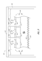
- FIG. 1 a schematic plan view of an example solar cell 100 is illustrated.
- the solar cell can include a silicon substrate 110 .
- the solar cell can also include a metal layer 150 formed on the silicon substrate 110 .
- the metal layer 150 can include a first and second busbar region 170 , 172 .
- Cross sectional lines 2 , 3 are shown.
- FIG. 2 represents a cross-section view of the solar cell 100 across the cross sectional line 2 .
- FIG. 3 represents a cross-section view of the solar cell 100 across the cross sectional line 3 .
- the solar cell can include a front side 102 which faces the sun during normal operation and a back side 104 opposite the front side 102 .
- the solar cell can include a silicon substrate 110 and first and second doped regions 112 , 114 .
- the solar cell can also include a first dielectric layer 122 .
- the solar cell can also include contact regions formed through the first dielectric layer 122 .
- the solar cell can include a first metal layer 130 .
- the first metal layer can be formed by a printing technique (e.g., screen printing).
- the first metal layer 130 can include metal particles, where the metal particles can be formed on the contact regions contacting the first and second doped regions 112 , 114 at contact locations 138 .
- the first metal layer 130 can be formed through a print process, such as through screen printing.
- the first metal layer can be a printed metal.
- Texturized regions 120 can be formed on the silicon substrate 110 , where texturized regions 120 provide additional light absorption.
- a second dielectric layer 124 can be formed on the texturized regions. As shown, the contact regions over different doped regions are separate.
- FIG. 3 illustrates another cross-section view of the solar cell of FIG. 1 .
- the first metal layer 130 and second metal layer 150 can be continuously disposed on the second doped region 114 .
- the first and second metal layer 130 , 150 can also be continuously disposed on the first doped region 112 .
- FIGS. 1-3 above show some example solar cell contact regions.
- the porosity of printed metal such as of the first metal layer 130 shown above, can increase the contact resistance of a solar cell. Increased contact resistance can be detrimental to the lifetime of charge carriers of the solar cell, degrading the overall solar cell performance. A low contact resistance is required to maximize the current flow of the solar cell.
- FIGS. 4-12 illustrate various structures corresponding to steps of one or more methods for forming a contact region on a solar cell. One or more methods are directed to overcoming the limitations discussed above. Details and embodiments are discussed below.
- the method can include providing a solar cell 200 having a front side 202 which faces the sun during normal operation and a back side 204 opposite the front side 202 .
- the solar cell 200 can include a silicon substrate 210 and first and second doped regions 212 , 214 .
- the solar cell can also include a first dielectric layer 222 .
- the solar cell can also include contact regions 226 formed through the first dielectric layer 222 .
- Texturized regions 220 can be formed on the silicon substrate 210 .
- a second dielectric layer 224 can be formed on the texturized regions.
- the method can include providing an electroless plating setup 180 .
- the electroless plating setup 180 can include the solar cell 200 immersed in an electroless plating medium 188 within a plating tank 186 .
- the solar cell 200 can be suspended by a holder 182 and a plurality of fixtures 184 .
- An auto-catalytic reaction e.g., electroless plating
- electroless plating can be induced within the electroless plating medium 188 to deposit a metal 240 over the contact region 226 of FIG. 4 forming a first metal contact 240 .
- the method can include electrolessly plating a metal 240 selected from the group consisting of nickel, gold, silver, rhodium, chromium, zinc, tin and cadmium. In an embodiment, the method can include electroless nickel plating to plate nickel to the contact region 226 of FIG. 4 .
- FIG. 6 illustrates a schematic plan view of an example solar cell of FIG. 5 .
- a back side 204 of the solar cell 200 is shown. Illustrated are the silicon substrate 210 , first metal contact 240 formed on the silicon substrate 210 .
- the first and second doped regions 212 , 214 are also shown. In an embodiment, the first and second doped regions can be formed in an interdigitated pattern as illustrated.
- the first metal contact 240 can include a first and second busbar region 270 , 272 .
- Cross sectional lines 7 , 8 are shown.
- FIG. 7 represents a cross-section view of the solar cell of FIG. 5 across the cross sectional line 7 .
- FIG. 8 represents a cross-section view of the solar cell 200 of FIG. 5 across the cross sectional line 8 .
- the solar cell 200 can include a first metal contact 240 formed over the first and second doped regions 212 , 214 . As shown, the first metal contact 240 formed over different doped regions are separated (e.g., not non-continuous or not connected).
- FIG. 8 illustrates another cross-section view of the solar cell of FIG. 6 .
- FIG. 8 represents the cross-section view of the solar cell across the cross sectional line 8 .
- the first metal contact 240 can be separated (e.g., not continuous or not connected) forming point contacts.
- point contacts provide low contact resistance.
- the point contacts can lower the cost for the formation of the first metal contact 240 (e.g., less material needed to manufacture point as compared to the line contacts seen in FIGS. 1-3 , point contacts have less area in comparison to line contacts).
- FIG. 9 illustrates a schematic plan view of an example solar cell of FIGS. 5-8 subsequent to the formation of a first metal paste 232 .
- the first metal paste 232 can be formed in an interdigitated pattern as illustrated.
- Cross sectional lines 10 , 11 are also shown.
- FIG. 10 represents a cross-section view of the solar cell 200 across the cross sectional line 10 .
- FIG. 11 represents a cross-section view of the solar cell 200 across the cross sectional line 11 .
- the method can include forming a first metal paste 232 having a printed metal, or metal particles, over the first metal contact 240 .
- the printed metal can be aluminum.
- the first metal paste 232 can be an aluminum paste.
- the printed metal can be aluminum particles.
- the first metal paste can be deposited by a printing technique.
- the first metal paste can be deposited by inkjet printing or screen printing.
- the metal paste comprises depositing an aluminum paste.
- the first metal paste (e.g., aluminum paste) can be formed with a thickness of at least 0.5 microns.
- FIG. 11 illustrates still another step in a method for forming a contact region for a solar cell.
- the method can include heating 260 the first metal paste 232 , where the heating removes a cohesive matrix 234 which can hold the printed metal together as required for dispensing.
- the curing 260 forms a first metal layer 230 from the first metal paste 232 , where the first metal layer 230 can include printed metal or metal particles.
- the first metal contact can be annealed.
- the method includes using an annealing temperature at least equal to 550° C.
- the method can include providing an electrolytic plating setup 290 including a solar cell immersed in an electrolytic plating medium 298 within a plating tank 296 .
- the method can include suspending the solar cell by a holder 292 and a plurality of fixtures 294 similar to the above.
- the method can include providing an anode 254 connected to an external power supply by a wire or an interconnect 256 .
- the method can include inducing a current, provided by the anode 254 coupled with the external power supply, within the electrolytic plating medium 298 , which may allow for the flow of electrons within the medium and further allow for electrolytic plating of a metal such as, but not limited to, copper, tin, aluminum, silver, gold, chromium, iron, nickel, zinc, ruthenium, palladium, and platinum.
- the method can include performing an electrolytic plating process to form a second metal layer 250 on the first metal layer 230 of the solar cell 200 .
- the method can further include electrolyticly plating a third metal layer to the second metal layer 250 using the same electrolytic plating setup 290 and methods mentioned above.
- FIG. 13 illustrates a schematic plan view of the solar cell subsequent to the methods of FIGS. 4-12 .
- the second metal layer metal 250 can be formed in an interdigitated pattern.
- Cross sectional lines 14 , 15 are also shown.
- FIG. 14 represents a cross-section view of the solar cell 200 across line 14 .
- FIG. 15 represents a cross-section view of the solar cell 200 across line 15 .
- the solar cell 200 can include a first metal contact 240 formed over the first and second doped regions 212 , 214 .
- the first metal contact 240 is in electrical connection 242 with the first and second doped regions 212 , 214 .
- the first metal layer 230 can be formed over the first metal contact 240 .
- the second metal layer 250 can be formed over the first metal layer 230 .
- a third metal layer 252 can be formed over the second metal layer 250 .
- a third metal layer 252 need not be formed.
- the first metal contact 240 can be separate (e.g., not physically or electrically connected, non-continuous) between different contact openings and/or doped regions.
- FIG. 15 illustrates a cross-section view of the solar cell of FIG. 13 .
- the first metal contact 240 can be separate (e.g., not physically or electrically connected, non-continuous) between different contact openings and/or doped regions.
- the first metal contact forms point contacts.
- the first, second and third metal layers 230 , 250 , 252 can be continuous, e.g., electrically connecting contact openings, doped regions and/or metal contacts 240 .
- at least two contact openings, doped regions and/or metal contacts 240 can be electrically connected.
- a third metal layer 252 need not be formed.
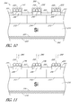
- FIG. 16 illustrates another solar cell 300 , according to some embodiments.
- the solar cell 300 can include a front side 302 which faces the sun during normal operation and a back side 304 opposite the front side 302 .
- the solar cell 300 can include a silicon substrate 310 having first and second doped polysilicon regions 312 , 314 .
- the first and second doped polysilicon regions 312 , 314 can be grown by a thermal process.
- a tunnel oxide region 308 can be formed between the first and second doped polysilicon regions and the silicon substrate 310 .
- the first and second doped polysilicon regions 312 , 314 can each include a doping material but is not limited to a positive-type dopant such as boron and a negative-type dopant such as phosphorous.
- a first dielectric layer 322 can be formed over the first and second doped polysilicon regions 312 , 314 .
- the solar cell 300 can also include a texturized surface 320 for additional light absorption and a second dielectric layer 324 formed over the texturized surface 320 .
- the first and second dielectric region can include silicon nitride.
- a trench region 328 can separate contact regions.
- the trench region 328 separates contact regions of different polarity.
- the trench region can be texturized as shown for additional light absorption from the back side of the solar cell.
- contact regions formed on the solar cell 300 can include a first metal contact 340 , a first metal layer 330 , a second metal layer 350 and a third metal layer 352 .
- the first metal contact 340 can be formed over the first and second doped regions 312 , 314 .
- the first metal contact can be formed by electroless plating.
- the first metal contact 340 form point contacts.
- the first metal layer 330 can be formed over the first metal contact 340 .
- the first metal layer can be formed by depositing and curing a first metal paste having a printed metal.
- the printed metal can be aluminum.
- the second metal layer 350 can be formed over the first metal layer 330 .
- the third metal layer 352 can be formed over the second metal layer 350 .
- the second and third metal layer 350 , 352 can be formed by electrolytic plating.
- a third metal layer 352 need not be formed.
- the solar cells shown in FIG. 15 can be back contact solar cells. Although a particular front contact solar cell structure is shown, various other front contact solar cell structures exist, where the said methods described above are applicable and are not limited to the above structures and methods mentioned wherein.
- the solar cell 400 can include a front side 402 which faces the sun during normal operation and a back side 404 opposite the front side 402 .
- the solar cell 400 can include a silicon substrate 310 having first and second doped regions 412 , 414 .
- the first and second doped polysilicon regions 412 , 414 can be grown by a thermal process.
- a tunnel oxide region 408 can be formed between the first and second doped regions 412 , 414 and the silicon substrate 410 .
- the first and second doped regions 412 , 414 can each include a doping material but is not limited to a positive-type dopant such as boron and a negative-type dopant such as phosphorous.
- a first dielectric layer 424 can be formed over the first doped regions 412 .
- a second dielectric layer 422 can be formed over the second doped regions 414 .
- the solar cell 400 can also include a texturized surface 420 for additional light absorption and a second dielectric layer 424 formed over the texturized surface 420 .
- the first and second dielectric region can include silicon nitride.
- contact regions formed on the solar cell 400 can include a first metal contact 440 , a first metal layer 430 , a second metal layer 450 and a third metal layer 452 .
- the first metal contact 340 can be formed over the first and second doped regions 412 , 414 .
- the first metal contact 440 can be formed by electroless plating.
- the first metal contacts 440 can be point contacts.
- the first metal layer 430 can be formed over the first metal contact 440 .
- the first metal layer 430 can be formed by depositing and curing a first metal paste having a printed metal.
- the printed metal can be aluminum.
- the second metal layer 450 can be formed over the first metal layer 430 .
- the third metal layer 452 can be formed over the second metal layer 450 .
- the second and third metal layer 450 , 452 can be formed by electrolytic plating.
- a third metal layer 452 need not be formed.
- front contact solar cell structure Although a particular front contact solar cell structure is shown, various other front contact solar cell structures exist, where the said methods described above are applicable and are not limited to the above structures and methods mentioned wherein.
- FIG. 18 illustrates a flow chart of an embodiment for an example method for forming a contact region on a solar cell.
- the method can include providing a solar cell having a front side which faces the sun during normal operation, a back side opposite the front side and a silicon substrate.
- At 502 at least one contact opening can be formed through a first dielectric layer above a silicon substrate of the solar cell, where the silicon substrate can include at least one doped region.
- a first metal contact can be electrolessly plated within at least one contact opening on at least one doped region of the silicon substrate.
- a first metal paste can be deposited above at least one contact opening, where the first metal paste in in electrical connection to the first metal contact.
- the first metal paste can be formed by screen printing.
- the first metal paste can be cured to form a first metal layer.
- the first metal contact, first metal layer and the silicon substrate can be heated.
- a second metal layer can be formed on the first metal layer where the first metal contact and the first metal layer electrically couple the second metal layer to the at least one doped region.
- FIG. 19 flow chart illustrating another example method for forming a contact region on a solar cell is shown.
- the method can include providing a solar cell having a front side which faces the sun during normal operation, a back side opposite the front side and a silicon substrate.
- At 512 at least one contact opening can be formed through a first dielectric layer above a silicon substrate of the solar cell, the silicon substrate having at least one doped region.
- the first metal paste can be formed by screen printing.
- At 513 at least one nickel contact can be electrollessly plated within at least one contact opening above at least one doped region of the silicon substrate.
- an aluminum paste can be deposited above, or over, at least one contact opening, where the aluminum paste electrically couples to at least one contact opening.
- the aluminum paste can be cured to form a layer of aluminum.
- At 516 at least one nickel contact, layer of aluminum and silicon substrate can be annealed to a temperature of at least 550° C.
- a second metal layer can be electrolyticly plated on the layer of aluminum, where at least one nickel contact and layer of aluminum electrically couples the second metal layer to at least one doped region.
- FIG. 20 illustrates still another example method for forming a contact region on a solar cell.
- a solar cell having a front side which faces the sun during normal operation, a back side opposite the front side and a silicon substrate.
- At 522 , at least one doped polysilicon region can be formed above, or over, a silicon substrate.
- At 523 at least one contact opening through a first dielectric layer above, or over, at least one doped polysilicon region, where at least one doped polysilicon region is formed between the first dielectric layer and silicon substrate.
- the first metal paste can be formed by screen printing.
- At 524 at least one nickel contact can be electrolessly plated within at least one contact opening above, or over, at least one doped polysilicon region of the silicon substrate.
- an aluminum paste can be formed above at least one contact opening, where the aluminum paste contacts at least one nickel contact and electrically couples at least one contact opening.
- the aluminum paste can be cured to form a layer of aluminum.
- At 527 at least one nickel contact, layer of aluminum and the silicon substrate can be annealed to a temperature of at least 550° C.
- a second metal layer can be electrolyticly plated on the layer of aluminum, where at least one nickel contact and the layer of aluminum electrically couples the second metal layer to at least one doped polysilicon region.
Landscapes
- Photovoltaic Devices (AREA)
- Engineering & Computer Science (AREA)
- Life Sciences & Earth Sciences (AREA)
- Sustainable Development (AREA)
- Sustainable Energy (AREA)
- Electrodes Of Semiconductors (AREA)
- Manufacturing & Machinery (AREA)
Abstract
Description
Claims (15)
Priority Applications (9)
| Application Number | Priority Date | Filing Date | Title |
|---|---|---|---|
| SG11201507008UA SG11201507008UA (en) | 2013-03-15 | 2014-03-14 | Conductivity enhancement of solar cells |
| MYPI2015002303A MY175806A (en) | 2013-03-15 | 2014-03-14 | Conductivity enhancement of solar cells |
| KR1020157028797A KR102242269B1 (en) | 2013-03-15 | 2014-03-14 | Conductivity enhancement of solar cells |
| MX2015013100A MX349018B (en) | 2013-03-15 | 2014-03-14 | Conductivity enhancement of solar cells. |
| PCT/US2014/029644 WO2014145009A1 (en) | 2013-03-15 | 2014-03-14 | Conductivity enhancement of solar cells |
| US14/211,353 US10074753B2 (en) | 2013-03-15 | 2014-03-14 | Conductivity enhancement of solar cells |
| AU2014233487A AU2014233487B2 (en) | 2013-03-15 | 2014-03-14 | Conductivity enhancement of solar cells |
| JP2016503178A JP6378748B2 (en) | 2013-03-15 | 2014-03-14 | Improving the conductivity of solar cells |
| TW103110008A TWI675491B (en) | 2013-03-15 | 2014-03-17 | Conductivity enhancement of solar cells |
Applications Claiming Priority (2)
| Application Number | Priority Date | Filing Date | Title |
|---|---|---|---|
| US201361800188P | 2013-03-15 | 2013-03-15 | |
| US14/211,353 US10074753B2 (en) | 2013-03-15 | 2014-03-14 | Conductivity enhancement of solar cells |
Publications (2)
| Publication Number | Publication Date |
|---|---|
| US20140261671A1 US20140261671A1 (en) | 2014-09-18 |
| US10074753B2 true US10074753B2 (en) | 2018-09-11 |
Family
ID=51521942
Family Applications (1)
| Application Number | Title | Priority Date | Filing Date |
|---|---|---|---|
| US14/211,353 Active 2036-03-29 US10074753B2 (en) | 2013-03-15 | 2014-03-14 | Conductivity enhancement of solar cells |
Country Status (11)
| Country | Link |
|---|---|
| US (1) | US10074753B2 (en) |
| EP (1) | EP2973734A4 (en) |
| JP (1) | JP6378748B2 (en) |
| KR (1) | KR102242269B1 (en) |
| CN (1) | CN105144398B (en) |
| AU (1) | AU2014233487B2 (en) |
| MX (1) | MX349018B (en) |
| MY (1) | MY175806A (en) |
| SG (1) | SG11201507008UA (en) |
| TW (1) | TWI675491B (en) |
| WO (1) | WO2014145009A1 (en) |
Families Citing this family (8)
| Publication number | Priority date | Publication date | Assignee | Title |
|---|---|---|---|---|
| US9293624B2 (en) * | 2012-12-10 | 2016-03-22 | Sunpower Corporation | Methods for electroless plating of a solar cell metallization layer |
| WO2016072415A1 (en) * | 2014-11-07 | 2016-05-12 | シャープ株式会社 | Photoelectric conversion element |
| US9520507B2 (en) * | 2014-12-22 | 2016-12-13 | Sunpower Corporation | Solar cells with improved lifetime, passivation and/or efficiency |
| WO2016114371A1 (en) * | 2015-01-16 | 2016-07-21 | シャープ株式会社 | Photoelectric conversion element, solar cell module equipped with same, and solar-light-generating system |
| WO2016147924A1 (en) * | 2015-03-13 | 2016-09-22 | シャープ株式会社 | Photoelectric conversion element and photoelectric conversion module |
| US9871150B1 (en) * | 2016-07-01 | 2018-01-16 | Sunpower Corporation | Protective region for metallization of solar cells |
| CN106252423B (en) * | 2016-08-15 | 2017-12-29 | 国网山西省电力公司大同供电公司 | A kind of novel photovoltaic battery and preparation method thereof |
| CN117059681B (en) | 2023-10-09 | 2024-03-29 | 晶科能源(海宁)有限公司 | Solar cells and manufacturing methods thereof, photovoltaic modules |
Citations (23)
| Publication number | Priority date | Publication date | Assignee | Title |
|---|---|---|---|---|
| JPS5426675A (en) | 1977-07-29 | 1979-02-28 | Matsushita Electric Ind Co Ltd | Manufacture for semiconductor device |
| US5011565A (en) * | 1989-12-06 | 1991-04-30 | Mobil Solar Energy Corporation | Dotted contact solar cell and method of making same |
| US5468652A (en) | 1993-07-14 | 1995-11-21 | Sandia Corporation | Method of making a back contacted solar cell |
| US20030172969A1 (en) | 2000-08-14 | 2003-09-18 | Jenson Jens Dahl | Process for depositing metal contacts on a buried grid solar cell and solar cell obtained by the process |
| US20060060238A1 (en) | 2004-02-05 | 2006-03-23 | Advent Solar, Inc. | Process and fabrication methods for emitter wrap through back contact solar cells |
| US20070148336A1 (en) | 2005-11-07 | 2007-06-28 | Robert Bachrach | Photovoltaic contact and wiring formation |
| US7339110B1 (en) | 2003-04-10 | 2008-03-04 | Sunpower Corporation | Solar cell and method of manufacture |
| US20080128268A1 (en) | 2006-12-01 | 2008-06-05 | Applied Materials, Inc. | High-aspect ratio anode and apparatus for high-speed electroplating on a solar cell substrate |
| US20080210301A1 (en) * | 2003-04-10 | 2008-09-04 | Sunpower Corporation | Metal contact structure for solar cell and method of manufacture |
| US20090139568A1 (en) | 2007-11-19 | 2009-06-04 | Applied Materials, Inc. | Crystalline Solar Cell Metallization Methods |
| US20090239331A1 (en) | 2008-03-24 | 2009-09-24 | Palo Alto Research Center Incorporated | Methods for forming multiple-layer electrode structures for silicon photovoltaic cells |
| JP2009290105A (en) | 2008-05-30 | 2009-12-10 | Sharp Corp | Solar battery, method of manufacturing solar battery, and solar battery module |
| US7633006B1 (en) | 2005-08-11 | 2009-12-15 | Sunpower Corporation | Back side contact solar cell with doped polysilicon regions |
| US20100032011A1 (en) | 2006-09-29 | 2010-02-11 | Erik Sauar | Back contacted solar cell |
| US20100124619A1 (en) | 2008-11-14 | 2010-05-20 | Palo Alto Research Center Incorporated | Solar cell metallization using inline electroless plating |
| CN101764180A (en) | 2009-12-31 | 2010-06-30 | 中山大学 | Method for manufacturing local front-surface field N-type solar cell |
| US20110192316A1 (en) | 2010-02-05 | 2011-08-11 | E-Chem Enterprise Corp. | Electroless plating solution for providing solar cell electrode |
| US20110195542A1 (en) | 2010-02-05 | 2011-08-11 | E-Chem Enterprise Corp. | Method of providing solar cell electrode by electroless plating and an activator used therein |
| JP2012060123A (en) | 2010-09-10 | 2012-03-22 | Samsung Electro-Mechanics Co Ltd | Forming method of conductive electrode structure, manufacturing method of solar cell including the same, and solar cell manufactured by the manufacturing method |
| EP2479802A1 (en) | 2009-09-15 | 2012-07-25 | Sharp Kabushiki Kaisha | Solar cell module and method for manufacturing same |
| KR101198870B1 (en) | 2011-11-07 | 2012-11-07 | 엘지전자 주식회사 | Solar cell and method for manufacturing the same |
| JP2012216646A (en) | 2011-03-31 | 2012-11-08 | Mitsubishi Electric Corp | Manufacturing method of solar cell |
| US20140174518A1 (en) * | 2012-12-21 | 2014-06-26 | Junbo Wu | Enhanced adhesion of seed layer for solar cell conductive contact |
Family Cites Families (5)
| Publication number | Priority date | Publication date | Assignee | Title |
|---|---|---|---|---|
| JPS5929474A (en) * | 1982-08-11 | 1984-02-16 | Toshiba Corp | Solar battery |
| JPS60140882A (en) * | 1983-12-28 | 1985-07-25 | Hitachi Ltd | Paste materials for semiconductor manufacturing |
| JP2009135338A (en) | 2007-11-30 | 2009-06-18 | Sanyo Electric Co Ltd | Solar cell and method for manufacturing solar cell |
| JP5449849B2 (en) * | 2009-04-30 | 2014-03-19 | シャープ株式会社 | Solar cell and method for manufacturing the same |
| US8779280B2 (en) * | 2009-08-18 | 2014-07-15 | Lg Electronics Inc. | Solar cell and method of manufacturing the same |
-
2014
- 2014-03-14 MY MYPI2015002303A patent/MY175806A/en unknown
- 2014-03-14 WO PCT/US2014/029644 patent/WO2014145009A1/en not_active Ceased
- 2014-03-14 US US14/211,353 patent/US10074753B2/en active Active
- 2014-03-14 CN CN201480015814.0A patent/CN105144398B/en active Active
- 2014-03-14 JP JP2016503178A patent/JP6378748B2/en active Active
- 2014-03-14 MX MX2015013100A patent/MX349018B/en active IP Right Grant
- 2014-03-14 AU AU2014233487A patent/AU2014233487B2/en active Active
- 2014-03-14 EP EP14763695.5A patent/EP2973734A4/en not_active Withdrawn
- 2014-03-14 KR KR1020157028797A patent/KR102242269B1/en active Active
- 2014-03-14 SG SG11201507008UA patent/SG11201507008UA/en unknown
- 2014-03-17 TW TW103110008A patent/TWI675491B/en active
Patent Citations (26)
| Publication number | Priority date | Publication date | Assignee | Title |
|---|---|---|---|---|
| JPS5426675A (en) | 1977-07-29 | 1979-02-28 | Matsushita Electric Ind Co Ltd | Manufacture for semiconductor device |
| US5011565A (en) * | 1989-12-06 | 1991-04-30 | Mobil Solar Energy Corporation | Dotted contact solar cell and method of making same |
| US5468652A (en) | 1993-07-14 | 1995-11-21 | Sandia Corporation | Method of making a back contacted solar cell |
| US20030172969A1 (en) | 2000-08-14 | 2003-09-18 | Jenson Jens Dahl | Process for depositing metal contacts on a buried grid solar cell and solar cell obtained by the process |
| US7339110B1 (en) | 2003-04-10 | 2008-03-04 | Sunpower Corporation | Solar cell and method of manufacture |
| US20080210301A1 (en) * | 2003-04-10 | 2008-09-04 | Sunpower Corporation | Metal contact structure for solar cell and method of manufacture |
| US20060060238A1 (en) | 2004-02-05 | 2006-03-23 | Advent Solar, Inc. | Process and fabrication methods for emitter wrap through back contact solar cells |
| JP2008512858A (en) | 2004-09-07 | 2008-04-24 | アドベント ソーラー,インク. | Manufacturing process and manufacturing method of emitter wrap through back contact solar cell |
| US7633006B1 (en) | 2005-08-11 | 2009-12-15 | Sunpower Corporation | Back side contact solar cell with doped polysilicon regions |
| US20070148336A1 (en) | 2005-11-07 | 2007-06-28 | Robert Bachrach | Photovoltaic contact and wiring formation |
| US20100032011A1 (en) | 2006-09-29 | 2010-02-11 | Erik Sauar | Back contacted solar cell |
| US20080128268A1 (en) | 2006-12-01 | 2008-06-05 | Applied Materials, Inc. | High-aspect ratio anode and apparatus for high-speed electroplating on a solar cell substrate |
| US20090139568A1 (en) | 2007-11-19 | 2009-06-04 | Applied Materials, Inc. | Crystalline Solar Cell Metallization Methods |
| US20090239331A1 (en) | 2008-03-24 | 2009-09-24 | Palo Alto Research Center Incorporated | Methods for forming multiple-layer electrode structures for silicon photovoltaic cells |
| JP2009290105A (en) | 2008-05-30 | 2009-12-10 | Sharp Corp | Solar battery, method of manufacturing solar battery, and solar battery module |
| EP2284907A1 (en) | 2008-05-30 | 2011-02-16 | Sharp Kabushiki Kaisha | Solar battery, method for manufacturing solar battery, and solar battery module |
| US20110114179A1 (en) | 2008-05-30 | 2011-05-19 | Yasushi Funakoshi | Solar battery, method for manufacturing solar battery, and solar cell module |
| US20100124619A1 (en) | 2008-11-14 | 2010-05-20 | Palo Alto Research Center Incorporated | Solar cell metallization using inline electroless plating |
| EP2479802A1 (en) | 2009-09-15 | 2012-07-25 | Sharp Kabushiki Kaisha | Solar cell module and method for manufacturing same |
| CN101764180A (en) | 2009-12-31 | 2010-06-30 | 中山大学 | Method for manufacturing local front-surface field N-type solar cell |
| US20110192316A1 (en) | 2010-02-05 | 2011-08-11 | E-Chem Enterprise Corp. | Electroless plating solution for providing solar cell electrode |
| US20110195542A1 (en) | 2010-02-05 | 2011-08-11 | E-Chem Enterprise Corp. | Method of providing solar cell electrode by electroless plating and an activator used therein |
| JP2012060123A (en) | 2010-09-10 | 2012-03-22 | Samsung Electro-Mechanics Co Ltd | Forming method of conductive electrode structure, manufacturing method of solar cell including the same, and solar cell manufactured by the manufacturing method |
| JP2012216646A (en) | 2011-03-31 | 2012-11-08 | Mitsubishi Electric Corp | Manufacturing method of solar cell |
| KR101198870B1 (en) | 2011-11-07 | 2012-11-07 | 엘지전자 주식회사 | Solar cell and method for manufacturing the same |
| US20140174518A1 (en) * | 2012-12-21 | 2014-06-26 | Junbo Wu | Enhanced adhesion of seed layer for solar cell conductive contact |
Non-Patent Citations (13)
| Title |
|---|
| "Principles and Technology of Photovoltaic Cells", Excerpts from the Chinese book, p. 201, line 8-9, English translation with Mar. 30, 2017, second office action, 4 pgs. |
| Decision of Rejection for Chinese Patent Application No. 2014800158140, dated May 4, 2018; 9 pgs. |
| European Search Report and Search Opinion from EP 14763695.5 dated Mar. 16, 2016, 7 pgs. |
| Examination Report 4 from Australian Patent Application No. 2014233487, dated Mar. 13, 2018, 3 pgs. |
| Examination Report No. 1 from Australian Patent Application No. 2014233487 dated Jul. 22, 2017, 3 pgs. |
| First Office Action for Chinese Patent Application No. 201480015814.0 dated Aug. 22, 2016, 22 pgs., with English translation. |
| International Preliminary Report on Patentability from PCT/US2014/029644 dated Sep. 24, 2015, 12 pgs. |
| International Search Report and Written Opinion for International Application No. PCT/US2014/029644 dated Jul. 17, 2014, 15 pages. |
| Non-Final Notice of Reasons for Rejection from Japanese Patent Application No. 2016-503178 dated Jan. 30, 2018, 6 pgs. |
| Non-Final Office Action for Mexico Patent Application No. MX/a/2015/013100 dated Nov. 17, 2016, 5 pgs., with English translation. |
| P212139 Buried Contract Solar Cells_PVEducation, Wayback Machine, report from May 20, 2012, viewed on the internet Feb. 13, 2018, 2 pgs. |
| Second Office Action for Chinese Patent Application No. 201480015814.0 dated Mar. 30, 2017, 10 pgs., with English translation. |
| Third Written Opinion from Intellectual Property Office of Singapore for Singapore Patent Application No. 11201507008U, dated May 2, 2018, 5 pgs. |
Also Published As
| Publication number | Publication date |
|---|---|
| TWI675491B (en) | 2019-10-21 |
| JP6378748B2 (en) | 2018-08-22 |
| KR102242269B1 (en) | 2021-04-19 |
| EP2973734A1 (en) | 2016-01-20 |
| SG11201507008UA (en) | 2015-10-29 |
| MY175806A (en) | 2020-07-09 |
| CN105144398A (en) | 2015-12-09 |
| CN105144398B (en) | 2019-04-12 |
| KR20150132322A (en) | 2015-11-25 |
| AU2014233487A1 (en) | 2015-09-17 |
| EP2973734A4 (en) | 2016-04-13 |
| TW201448236A (en) | 2014-12-16 |
| WO2014145009A1 (en) | 2014-09-18 |
| JP2016514901A (en) | 2016-05-23 |
| MX349018B (en) | 2017-07-07 |
| MX2015013100A (en) | 2016-01-22 |
| US20140261671A1 (en) | 2014-09-18 |
| AU2014233487B2 (en) | 2018-08-09 |
Similar Documents
| Publication | Publication Date | Title |
|---|---|---|
| US10074753B2 (en) | Conductivity enhancement of solar cells | |
| KR102219630B1 (en) | Methods for electroless conductivity enhancement of solar cell metallization | |
| EP3123525B1 (en) | Solar cells with tunnel dielectrics | |
| US9847438B2 (en) | Reduced contact resistance and improved lifetime of solar cells | |
| US20180190837A1 (en) | Metallization structures for solar cells | |
| US11682744B2 (en) | Solar cells having hybrid architectures including differentiated P-type and N-type regions | |
| US10056506B2 (en) | Firing metal with support |
Legal Events
| Date | Code | Title | Description |
|---|---|---|---|
| AS | Assignment |
Owner name: SUNPOWER CORPORATION, CALIFORNIA Free format text: ASSIGNMENT OF ASSIGNORS INTEREST;ASSIGNOR:ZHU, XI;REEL/FRAME:032564/0679 Effective date: 20140319 |
|
| STCF | Information on status: patent grant |
Free format text: PATENTED CASE |
|
| MAFP | Maintenance fee payment |
Free format text: PAYMENT OF MAINTENANCE FEE, 4TH YEAR, LARGE ENTITY (ORIGINAL EVENT CODE: M1551); ENTITY STATUS OF PATENT OWNER: LARGE ENTITY Year of fee payment: 4 |
|
| AS | Assignment |
Owner name: MAXEON SOLAR PTE. LTD., SINGAPORE Free format text: ASSIGNMENT OF ASSIGNORS INTEREST;ASSIGNOR:SUNPOWER CORPORATION;REEL/FRAME:062699/0875 Effective date: 20221214 |
|
| AS | Assignment |
Owner name: DB TRUSTEES (HONG KONG) LIMITED, HONG KONG Free format text: SECURITY INTEREST;ASSIGNOR:MAXEON SOLAR PTE. LTD.;REEL/FRAME:067637/0598 Effective date: 20240531 |
|
| AS | Assignment |
Owner name: DB TRUSTEES (HONG KONG) LIMITED, HONG KONG Free format text: SECOND LIEN SECURITY INTEREST AGREEMENT;ASSIGNOR:MAXEON SOLAR PTE. LTD;REEL/FRAME:071343/0553 Effective date: 20240620 |
|
| AS | Assignment |
Owner name: DB TRUSTEES (HONG KONG) LIMITED, HONG KONG Free format text: SECURITY INTEREST;ASSIGNOR:MAXEON SOLAR PTE. LTD.;REEL/FRAME:067924/0062 Effective date: 20240620 |
|
| AS | Assignment |
Owner name: MAXEON SOLAR PTE. LTD., SINGAPORE Free format text: ASSIGNMENT OF ASSIGNORS INTEREST;ASSIGNORS:TOTALENERGIES SE;TOTALENERGIES SOLAR INTL;REEL/FRAME:072514/0911 Effective date: 20250708 |