US10074004B2 - Capacitive fingerprint sensor with integrator - Google Patents
Capacitive fingerprint sensor with integrator Download PDFInfo
- Publication number
- US10074004B2 US10074004B2 US15/230,368 US201615230368A US10074004B2 US 10074004 B2 US10074004 B2 US 10074004B2 US 201615230368 A US201615230368 A US 201615230368A US 10074004 B2 US10074004 B2 US 10074004B2
- Authority
- US
- United States
- Prior art keywords
- integrator
- level
- port
- input terminal
- reference voltage
- Prior art date
- Legal status (The legal status is an assumption and is not a legal conclusion. Google has not performed a legal analysis and makes no representation as to the accuracy of the status listed.)
- Active, expires
Links
Images


Classifications
-
- G—PHYSICS
- G06—COMPUTING; CALCULATING OR COUNTING
- G06F—ELECTRIC DIGITAL DATA PROCESSING
- G06F3/00—Input arrangements for transferring data to be processed into a form capable of being handled by the computer; Output arrangements for transferring data from processing unit to output unit, e.g. interface arrangements
- G06F3/01—Input arrangements or combined input and output arrangements for interaction between user and computer
- G06F3/03—Arrangements for converting the position or the displacement of a member into a coded form
- G06F3/041—Digitisers, e.g. for touch screens or touch pads, characterised by the transducing means
- G06F3/044—Digitisers, e.g. for touch screens or touch pads, characterised by the transducing means by capacitive means
- G06F3/0445—Digitisers, e.g. for touch screens or touch pads, characterised by the transducing means by capacitive means using two or more layers of sensing electrodes, e.g. using two layers of electrodes separated by a dielectric layer
-
- G—PHYSICS
- G06—COMPUTING; CALCULATING OR COUNTING
- G06V—IMAGE OR VIDEO RECOGNITION OR UNDERSTANDING
- G06V40/00—Recognition of biometric, human-related or animal-related patterns in image or video data
- G06V40/10—Human or animal bodies, e.g. vehicle occupants or pedestrians; Body parts, e.g. hands
- G06V40/12—Fingerprints or palmprints
- G06V40/13—Sensors therefor
- G06V40/1306—Sensors therefor non-optical, e.g. ultrasonic or capacitive sensing
-
- G06K9/0002—
-
- G—PHYSICS
- G06—COMPUTING; CALCULATING OR COUNTING
- G06F—ELECTRIC DIGITAL DATA PROCESSING
- G06F3/00—Input arrangements for transferring data to be processed into a form capable of being handled by the computer; Output arrangements for transferring data from processing unit to output unit, e.g. interface arrangements
- G06F3/01—Input arrangements or combined input and output arrangements for interaction between user and computer
- G06F3/03—Arrangements for converting the position or the displacement of a member into a coded form
- G06F3/041—Digitisers, e.g. for touch screens or touch pads, characterised by the transducing means
- G06F3/0416—Control or interface arrangements specially adapted for digitisers
- G06F3/04166—Details of scanning methods, e.g. sampling time, grouping of sub areas or time sharing with display driving
-
- G—PHYSICS
- G06—COMPUTING; CALCULATING OR COUNTING
- G06F—ELECTRIC DIGITAL DATA PROCESSING
- G06F3/00—Input arrangements for transferring data to be processed into a form capable of being handled by the computer; Output arrangements for transferring data from processing unit to output unit, e.g. interface arrangements
- G06F3/01—Input arrangements or combined input and output arrangements for interaction between user and computer
- G06F3/03—Arrangements for converting the position or the displacement of a member into a coded form
- G06F3/041—Digitisers, e.g. for touch screens or touch pads, characterised by the transducing means
- G06F3/044—Digitisers, e.g. for touch screens or touch pads, characterised by the transducing means by capacitive means
Definitions
- the present invention relates to a capacitive fingerprint sensor, and particularly to a “C-Q-T” type capacitive fingerprint sensor with an integrator.
- C-V-T type capacitive distance sensors are disclosed for the first time in a Chinese invention patent with the title of “Capacitive Distance Sensor” and the application number of 201210403271.2.
- the “C-V-T” type capacitive distance sensors measuring circuits are simplified and under the same process conditions, the technical level of such sensors is higher than the internationally advanced level in 2012.
- the technology of Touch ID sensors installed in iPhone5S is proposed by Apple Inc. in 2013, the development and application of fingerprint sensor technologies are greatly pushed forward, and the consumer electronics market has huge demand and higher requirements for the fingerprint sensor technologies.
- Vt′ (Vs ⁇ Vt)*(Cd+Cg)/(Ct+Cd+Cg) that variation Vt′ of voltage Vt of an integrating capacitor during each iteration is negatively correlated with Vt.
- Vt′ causes gradual decrease of Vt, which further leads gradual decrease of Vt′, while smaller Vt′ is likely to be interfered by noise.
- a comparator flip will become either earlier or later, resulting in noise interference with output of the sensor.
- a relation between output time of the sensor and target capacitors Cg is convex nonlinear.
- the convex nonlinear relation may serve as a compensation measure for convex nonlinear conversion from distances to capacitance within a certain spatial scale, which has been explained in the above two Chinese invention patents with the titles of “Capacitive Distance Sensor” and “Capacitive Fingerprint Sensor”.
- the thickness of a dielectric layer between a sensing electrode and a target electrode in a commercial capacitive fingerprint sensor is increased from an order of magnitude of 10 um to an order of magnitude of 100 um, so that the distance-to-capacitance conversion relationship falls into an approximately linear region.
- the convex nonlinear conversion from output of the target electrode to output of the fingerprint sensor has become a disadvantage.
- a bus parasitic capacitor is calculated into the integrating capacitor, improving the discreteness of the integrating capacitor.
- manufacturing tolerance of the background capacitor will cause inconsistence among units in a fingerprint sensor array.
- One objective of the present invention is to provide a capacitive fingerprint sensor better in linearity and anti-noise capability.
- the present invention adopts the following technical schemes.
- a capacitive fingerprint sensor with an integrator comprises a sensing array, the integrator, a bus and a comparison circuit.
- the sensing array comprises a plurality of sensing units, wherein each sensing unit comprises a target electrode, a sensing electrode, a driving electrode, a first level driver, a second level driver, a line selection switch, an initialization switch and a first reference voltage, and an output terminal of each sensing unit is connected to the bus.
- An input terminal of the integrator is connected to the bus, and an output terminal of the integrator is connected to an input terminal of the comparison circuit.
- the input terminal of the comparison circuit is connected to an output terminal of the integrator, and the output terminal of the integrator is that of the capacitive fingerprint sensor.
- the sensing electrode comprises one or more electrodes, is connected to a first port of the initialization switch, and is connected to a first port of the line selection switch;
- the target electrode is a surface of a target to be measured, is connected to the first level driver and is positioned above the sensing electrode, wherein a dielectric layer is formed between the target electrode and the sensing electrode, and a target capacitor is formed between the target electrode and the sensing electrode.
- the driving electrode comprises one or more driving electrodes, is connected to the second level driver and is positioned below the sensing electrode, wherein another dielectric layer is formed between the driving electrode and the sensing electrode, and a driving capacitor is formed between the driving electrode and the sensing electrode.
- a control terminal of the first level driver is connected to a first level control signal, and an output terminal of the first level driver is connected to the target electrode.
- a control terminal of the second level driver is connected to a second level control signal, and an output terminal of the second level driver is connected to the driving electrode.
- a first port of the line selection switch is connected to the sensing electrode, and a second port of the line selection switch is connected to the output terminal of the sensing unit.
- a first port of the initialization switch is connected to the sensing electrode, and a second port of the initialization switch is connected to the first reference voltage.
- the first reference voltage is connected to the second port of the initialization switch.
- the first level driver outputs a level V 11 to the target electrode via a resistor when the first level control signal is low, and outputs a level V 12 to the target electrode via the resistor when the first level control signal is high.
- the first level driver outputs a level V 11 to a capacitor when the first level control signal is low, and outputs a level V 12 to the capacitor when the first level control signal is high, wherein the capacitor outputs an alternating current (AC) component of the levels V 11 and V 12 in a coupled manner to the target electrode.
- AC alternating current
- the first level driver outputs a level V 11 to a converting circuit when the first level control signal is low, and outputs a level V 12 to the converting circuit when the first level control signal is high, wherein the AC component of the levels V 11 and V 12 is converted to a reverse AC level through the converting circuit to be coupled to a ground level of the capacitive fingerprint sensor.
- the second level driver outputs a level V 21 to the driving electrode when the second level control signal is low, and outputs a level V 22 to the driving electrode when the second level control signal is high.
- the integrator comprises an amplifier, an integrating capacitor, a second reference voltage, a second reset switch, a third reset switch, a following switch and a fourth reference voltage.
- a first input terminal of the amplifier is connected to the input terminal of the integrator, a second input terminal of the amplifier is connected to the second reference voltage, and an output terminal of the amplifier is connected to that of the integrator.
- a first port of the integrating capacitor is connected to the first input terminal of the amplifier, and a second port of the integrating capacitor is connected to a first port of the third reset switch.
- the second reference voltage is connected to the second input terminal of the amplifier.
- a first port of the second reset switch is connected to the second reference voltage, and a second port of the second reset switch is connected to the first input terminal of the amplifier.
- a first port of the third reset switch is connected to the second port of the integrating capacitor, and a second port of the third reset switch is connected to the fourth reference voltage.
- a first port of the following switch is connected to the second port of the integrating capacitor, and a second port of the following switch is connected to the output terminal of the integrator.
- the fourth reference voltage is connected to the second port of the third reset switch.
- a reset time sequence of the integrator is as below: step 1 - 1 : turning off the following switch; step 1 - 2 : turning on the second reset switch, and turning on the third reset switch; step 1 - 3 : turning off the second reset switch, and turning off the third reset switch; and step 1 - 4 : turning on the following switch.
- the present invention may use a design of a simplified integrator, in which an amplifier is connected to be used as a unity-gain buffer to reset the integrator.
- the simplified integrator comprises the amplifier, an integrating capacitor, a second reference voltage and a first reset switch.
- a first input terminal of the amplifier is connected to the input terminal of the integrator, a second input terminal of the amplifier is connected to the second reference voltage, and an output terminal of the amplifier is connected to that of the integrator.
- the integrating capacitor comprises one or more capacitors, a first port of the integrating capacitor is connected to the first input terminal of the amplifier, and a second port of the integrating capacitor is connected to the output terminal of the amplifier.
- the second reference voltage is connected to the second input terminal of the amplifier.
- a first port of the first reset switch is connected to the first input terminal of the amplifier, and a second port of the first reset switch is connected to the output terminal of the amplifier.
- a reset time sequence of the integrator is as below: step 2 - 1 : turning on the first reset switch; and step 2 - 2 : turning off the first reset switch.
- the comparison circuit comprises a comparator and a third reference voltage.
- a first input terminal of the comparator is connected to an input terminal of the comparison circuit, a second input terminal of the comparator is connected to the third reference voltage, and an output terminal of the comparator is connected to that of the comparison circuit.
- the third reference voltage is connected to the second input terminal of the comparator.
- a coupling capacitor (equivalent to the target capacitor) is formed between the surface of a fingerprint to be measured (equivalent to the target electrode) and a capacitance measuring plate (equivalent to the sensing electrode); and distances from different regions on the surface of the fingerprint to be measured to different capacitance measuring plates in a corresponding sensor array are different, so do the target capacitors.
- the integrating capacitor is firstly charged to reach the fourth reference voltage, and then periodically discharges to the target capacitor. Based on the circuit and a control method designed in the present invention, a charge quantity of discharge to the target capacitor for each time is related to a capacity of the target capacitor; and for the same target capacitor, charge quantities of discharge for each time are the same.
- the comparison circuit outputs signal flip; and the times for signal flip are reciprocal values of discharge rates of the integrating capacitor, and the time change is approximately linear in a certain numerical interval.
- a sensing process of the sensor depends on “the capacity of the target capacitor-differences in discharge rates of the integrating capacitor-the time sequence of flips in the comparison circuit”, namely the “C-Q-T” process.
- the “C-Q-T” process is divided into a “C-Q” conversion process and a “Q-T” conversion process.
- the “C-Q” conversion process comprises two parts, namely resetting of the integrator and the integrating capacitor repeatedly discharging to the target capacitor.
- a reset process of the integrator is that the integrating capacitor is charged to reach the fourth reference voltage.
- a value of the second reference voltage be VREF 2
- a value of the fourth reference voltage be VREF 4
- the simplified reset circuit lies in that for voltages of the integrator in the above example, VREF 4 is equal to VREF 2 .
- step 3 - 1 turning off the line selection switch
- step 3 - 2 turning on the initialization switch, and connecting the first reference voltage to the sensing electrode
- step 3 - 3 setting the first level control signal to be high, and setting the second level control signal to be high
- step 3 - 4 turning off the initialization switch
- step 3 - 5 turning on the line selection switch
- step 3 - 6 setting the first level control signal to be low and setting the second level control signal to be low
- step 3 - 7 returning to step 3 - 1 .
- a value of the target capacitor be Cf
- a value of the driving capacitor be Cd
- a value of the parasitic capacitor in each sensing unit be Cb
- a value of the bus parasitic capacitor be Cp
- a value of the first reference voltage be VREF 1
- a value of the third reference voltage be VREF 3 .
- T ( Qr.end ⁇ Qr.rst )/ ⁇ Q (2)
- (Qr.end-Qr.rst) is a fixed value; and according to the equation (1), ⁇ Q is just a linear function of Cf.
- T is an integer, and the value of T represents the output of the “C-Q-T” type fingerprint sensor.
- ⁇ Q is just a linear function of Cf.
- ⁇ Q is a constant value, which means that charge quantities of discharge of the integrating capacitor for each time are the same, so that the change curve of the charge quantities in the integrating capacitor is linear.
- a circuit structure provided by the present invention has a variety of operating modes; and the first reference voltage, the second reference voltage, the first level driver and the second level driver may be reasonably designed according to requirements on cost, power consumption and sensitivity etc.
- FIG. 1 is a circuit diagram of a capacitive fingerprint sensor provided by the present invention
- FIG. 2 is a circuit diagram of a sensing unit provided by the present invention.
- FIG. 3 shows a first level driver according to a first embodiment
- FIG. 4 shows another first level driver according to a second embodiment
- FIG. 5 shows yet another first level driver according to a third embodiment
- FIG. 6 shows a schematic drawing of a second level driver
- FIG. 7 shows an integrator provided by the present invention according to a first embodiment
- FIG. 8 shows a main time sequence control and driving waveform of the integrator of the present invention shown in FIG. 7 ;
- FIG. 9 shows another integrator provided by the present invention according to a second embodiment
- FIG. 10 shows a main time sequence control and driving waveform of the integrator of the present invention shown in FIG. 9 ;
- FIG. 11 is a diagram of a comparison circuit provided by the present invention.
- FIG. 12 shows a comparison diagram of an output potential curve of the integrator and a third reference voltage of a comparator.
- FIG. 1 is a circuit diagram of a capacitive fingerprint sensor provided by the present invention.
- the capacitive fingerprint sensor provided by the present invention comprises a sensing array 1 , a bus 2 , an integrator 3 , a comparator module 4 and a bus parasitic capacitor 21 , wherein the sensing array 1 comprises a plurality of sensing unit 11 .
- FIG. 2 is a circuit diagram of a sensing unit provided by the present invention.
- each sensing unit 11 comprises a target electrode 111 , a sensing electrode 112 , a driving electrode 113 , a first level driver 114 , a second level driver 117 , a line selection switch 118 , an initialization switch 115 and a first reference voltage 116 .
- the sensing electrode 112 comprises one or more sensing electrodes, and is connected to a first port of the initialization switch 115 and a first port of the line selection switch 118 .
- the target electrode 111 is a surface of a target to be measured, is connected to the first level driver 114 and is positioned above the sensing electrode 112 , wherein a dielectric layer is formed between the target electrode 111 and the sensing electrode 112 , and a target capacitor 201 is formed between the target electrode 111 and the sensing electrode 112 .
- the driving electrode 113 comprises one or more driving electrodes, is connected to the second level driver 117 and is positioned below the sensing electrode 112 , wherein another dielectric layer is formed between the driving electrode 113 and the sensing electrode 112 , and a driving capacitor 202 is formed between the driving electrode 113 and the sensing electrode 112 .
- the first level driver 114 is connected to the target electrode 111 .
- the second level driver 117 is connected to the driving electrode 113 .
- a first port of the initialization switch 115 is connected to the sensing electrode 112 , and a second port of the initialization switch 115 is connected to the first reference voltage 116 .
- a first port of the line selection switch 118 is connected to the sensing electrode 112 , and a second port of the line selection switch 118 is connected to the output terminal of the sensing unit 111 .
- the output terminal of the sensing unit 111 is connected to the bus 2 .
- Each sensing unit 111 further comprises a background capacitor 203 therein.
- FIG. 3 shows a first level driver according to a first embodiment.
- the first level driver comprises an input level V 11 401 , another input level V 12 403 , a first level control signal 404 , a first level selector 402 and a resistor 405 .
- the input level V 11 401 is connected to a first input terminal of the first level selector 402 ; the input level V 12 403 is connected to a second input terminal of the first level selector 402 ; the first level control signal 404 is connected to a control terminal of the first level selector 402 ; an output terminal of the first level selector 402 is connected to a first port of the resistor 405 ; and a second port of the resistor 405 is connected to the target electrode 111 .
- the first level selector 402 outputs a first input terminal level when the first level control signal 404 is low, and outputs a second input terminal level when the first level control signal 404 is high.
- FIG. 4 shows another first level driver according to a second embodiment.
- the first level driver comprises an input level V 11 401 , another input level V 12 403 , a first level control signal 404 , a first level selector 402 and a capacitor 505 .
- the input level V 11 401 is connected to a first input terminal of the first level selector 402 ;
- the input level V 12 403 is connected to a second input terminal of the first level selector 402 ;
- the first level control signal 404 is connected to a control terminal of the first level selector 402 ;
- an output terminal of the first level selector 402 is connected to a first port of the capacitor 505 ; and a second port of the capacitor 505 is connected to the target electrode 111 .
- the first level selector 402 outputs a first input terminal level when the first level control signal 404 is low, and outputs a second input terminal level when the first level control signal 404 is high.
- FIG. 5 shows yet another first level driver according to a third embodiment.
- the first level driver comprises a phase inverter 603 , a signal converter 601 , a driving circuit 602 , a first level control signal 404 and a sensor ground level input terminal 605 .
- the first level control signal 404 is connected to an input terminal of the phase inverter 603 ; an output terminal of the phase inverter 603 is connected to an input terminal of the signal converter 601 ; an output terminal of the signal converter 601 is connected to a control terminal of the driving circuit 602 ; an output terminal of the driving circuit 602 is connected to the sensor ground level input terminal 605 ; and the target electrode 111 is grounded or suspended in the air.
- the signal converter 601 is configured to convert an input signal from a sensor ground level domain to a system ground level domain.
- the driving circuit 602 is configured to amplify an input terminal level and provide driving at the output terminal.
- FIG. 6 shows a schematic drawing of a second level driver.
- the second level driver comprises an input level V 21 501 , another input level V 22 503 , a second level control signal 504 and a second level selector 502 .
- the input level V 21 501 is connected to a first input terminal of the second level selector 502 ;
- the input level V 22 503 is connected to a second input terminal of the second level selector 502 ;
- the second level control signal 504 is connected to a control terminal of the second level selector 502 ;
- an output terminal of the second level selector 502 is connected to the driving electrode 113 .
- the second level selector 502 outputs a first input terminal level when the second level control signal 504 is low, and outputs a second input terminal level when the second level control signal 504 is high.
- FIG. 7 shows an integrator provided by the present invention according to a first embodiment.
- the integrator 3 comprises an amplifier 37 , an integrating capacitor 36 , a second reference voltage 31 , a second reset switch 34 , a third reset switch 35 , a following switch 32 and a fourth reference voltage 33 .
- a first port of the third reset switch 35 is connected to the second reference voltage 31 , and a second port of the third reset switch 35 is connected to a first input terminal of the amplifier 37 .
- a first port of the second reset switch 34 is connected to a first port of the integrating capacitor 36 , and a second port of the second reset switch 34 is connected to the fourth reference voltage 33 .
- a first port of the integrating capacitor 36 is connected to the first input terminal of the amplifier 37 , and a second port of the integrating capacitor 36 is connected to the first port of the second reset switch 34 .
- a first port of the following switch 32 is connected to the second port of the integrating capacitor 36 , and a second port of the following switch 32 is connected to the output terminal of the integrator 3 .
- a first input terminal of the amplifier 37 is connected to the input terminal of the integrator 3 , a second input terminal of the amplifier 37 is connected to the second reference voltage 31 , and an output terminal of the amplifier is connected to the output terminal of the integrator 3 .
- the input terminal of the integrator 3 is connected to the bus 2 , and the output terminal of the integrator 3 is connected to an input terminal of the comparison circuit 4 .
- FIG. 8 shows a main time sequence control and driving waveform of the integrator of the present invention shown in FIG. 7 .
- the main time sequence control process comprises: step 1 : turning off all switches in the circuit; step 2 : turning on the second reset switch 34 or the third reset switch 35 ; step 3 : turning off the second reset switch 34 or the third reset switch 35 ; step 4 : turning on the following switch 32 ; step 5 : turning off the line selection switch 118 ; step 6 : turning on the initialization switch 115 , and connecting the first reference voltage 116 to the sensing electrode 112 ; step 7 : setting the first level control signal 404 to be high and setting the second level control signal 504 to be high; step 8 : turning off the initialization switch 115 ; step 9 : turning on the line selection switch 118 ; step 10 : setting the first level control signal 404 to be low and setting the second level control signal 504 to be low; and step 11 : returning to step 5 .
- FIG. 9 shows a circuit diagram of an integrator provided by the present invention according to a second embodiment.
- the integrator 3 comprises an amplifier 37 , a second reference voltage 31 , an integrating capacitor 36 and a first reset switch 304 .
- a first input terminal of the amplifier 37 is connected to the input terminal of the integrator 3 , a second input terminal of the amplifier 37 is connected to the second reference voltage 31 , and an output terminal of the amplifier is connected to the output terminal of the integrator 3 .
- a first port of the integrating capacitor 36 is connected to the first input terminal of the amplifier 37 , and a second port of the integrating capacitor 36 is connected to the output terminal of the amplifier 37 .
- a first port of the first reset switch 304 is connected to the first input terminal of the amplifier 37 , and a second port of the first reset switch is 304 is connected to the output terminal of the amplifier 37 .
- FIG. 9 shows a simplified structure of the integrator 3 shown in FIG. 7 .
- FIG. 10 shows a main time sequence control and driving waveform of the integrator 3 of the present invention shown in FIG. 9 .
- an operation time sequence of the integrator 3 shown in FIG. 9 is changed only during resetting, while operation time sequences of other parts are the same.
- the first reset switch 304 is turned on, the amplifier 37 is connected to be used as the unity-gain buffer, the output terminal of the amplifier 37 is reset to a level of the second reference voltage 31 , and then the first reset switch 304 is turned off, but the output terminal of the amplifier 37 is kept at the level of the second reference voltage 31 through the integrating capacitor 36 , so that the output terminal of the integrator 3 is reset to the level of the second reference voltage 31 .
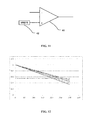
- FIG. 11 is a diagram of a comparison circuit 4 provided by the present invention. As shown in FIG. 11 , the comparison circuit 4 comprises a comparator 41 and a third reference voltage 42 .
- a first input terminal of the comparator 41 is connected to the output terminal of the amplifier 37 , a second input terminal of the comparator is 41 connected to the third reference voltage 42 , and an output terminal of the comparator 41 is connected to an output terminal of the comparison circuit 4 .
- the input terminal of the comparison circuit 4 is the output terminal of the integrator 3 , and the output of the comparison circuit 4 is that of the fingerprint sensor.
- FIG. 12 shows a comparison diagram of an output potential curve of the integrator 3 and a third reference voltage of the comparison circuit 4 .
- the change rates of the output of the integrator 3 will be different, so intersection points of the output of the integrator 3 and the third reference voltage 42 will be different, and locations of projections on a timeline will be different.
- the output of the comparison circuit 4 flips at the intersection points of the output of the integrator 3 and the third reference voltage 42 .
Applications Claiming Priority (3)
| Application Number | Priority Date | Filing Date | Title |
|---|---|---|---|
| CN201510309222 | 2015-06-08 | ||
| CN201510309222.6A CN105046194B (zh) | 2015-06-08 | 2015-06-08 | 一种包含积分器的电容指纹传感器 |
| CN201510309222.6 | 2015-06-08 |
Publications (2)
| Publication Number | Publication Date |
|---|---|
| US20170235993A1 US20170235993A1 (en) | 2017-08-17 |
| US10074004B2 true US10074004B2 (en) | 2018-09-11 |
Family
ID=54452723
Family Applications (1)
| Application Number | Title | Priority Date | Filing Date |
|---|---|---|---|
| US15/230,368 Active 2036-09-22 US10074004B2 (en) | 2015-06-08 | 2016-08-05 | Capacitive fingerprint sensor with integrator |
Country Status (3)
| Country | Link |
|---|---|
| US (1) | US10074004B2 (zh) |
| CN (1) | CN105046194B (zh) |
| TW (1) | TWI630533B (zh) |
Cited By (1)
| Publication number | Priority date | Publication date | Assignee | Title |
|---|---|---|---|---|
| US10410032B2 (en) * | 2016-03-02 | 2019-09-10 | Samsung Electronics Co., Ltd. | Fingerprint sensor, electronic device having the same, and method of operating the fingerprint sensor |
Families Citing this family (17)
| Publication number | Priority date | Publication date | Assignee | Title |
|---|---|---|---|---|
| CN105335737B (zh) * | 2015-12-02 | 2019-03-15 | 苏州迈瑞微电子有限公司 | 电容指纹传感器 |
| CN106775143B (zh) | 2015-12-31 | 2020-01-03 | 深圳市汇顶科技股份有限公司 | 积分电路及电容感测电路 |
| CN107368773A (zh) * | 2016-05-12 | 2017-11-21 | 戴孟均 | 一种指纹传感器及应用其的智能设备 |
| EP3321848B1 (en) * | 2016-09-27 | 2019-12-25 | Shenzhen Goodix Technology Co., Ltd. | Capacitive sensing circuit |
| EP3324331B1 (en) * | 2016-09-27 | 2020-11-25 | Shenzhen Goodix Technology Co., Ltd. | Capacitive sensing circuit |
| CN106462761B (zh) | 2016-10-27 | 2021-06-29 | 深圳市汇顶科技股份有限公司 | 电容式指纹传感器 |
| US10395084B2 (en) * | 2017-09-29 | 2019-08-27 | Superc-Touch Corporation | Fingerprint identification device |
| CN107704827B (zh) * | 2017-09-30 | 2024-03-12 | 苏州迈瑞微电子有限公司 | 一种光电传感器和具有其的光电传感器阵列 |
| CN107688798B (zh) * | 2017-09-30 | 2023-10-17 | 苏州迈瑞微电子有限公司 | 一种电荷型传感器和具有其的传感器阵列及积分电路失配调整参数的获取方法 |
| EP3493096B1 (en) * | 2017-10-18 | 2020-11-11 | Shenzhen Goodix Technology Co., Ltd. | Fingerprint sensor and terminal device |
| CN109697398B (zh) * | 2017-10-24 | 2023-09-01 | 苏州迈瑞微电子有限公司 | 一种传感器传感方法、电子装置、存储介质和终端设备 |
| EP3537336B1 (en) | 2017-11-07 | 2021-03-17 | Shenzhen Goodix Technology Co., Ltd. | Fingerprint sensor and terminal device |
| CN109460726B (zh) * | 2018-10-31 | 2020-07-31 | 上海海栎创微电子有限公司 | 一种电容式指纹信号的差分采集放大电路及其工作方法 |
| CN109631956A (zh) * | 2018-12-27 | 2019-04-16 | 苏州迈瑞微电子有限公司 | 一种电容式传感器及其校正方法 |
| US11301708B2 (en) * | 2019-10-01 | 2022-04-12 | Novatek Microelectronics Corp. | Image sensing circuit and method |
| CN112929017B (zh) * | 2021-02-02 | 2023-08-18 | 同源微(北京)半导体技术有限公司 | 一种提升复位速度的积分器电路 |
| US11967169B2 (en) * | 2021-09-28 | 2024-04-23 | Synaptics Incorporated | In-display capacitive fingerprint sensor |
Citations (5)
| Publication number | Priority date | Publication date | Assignee | Title |
|---|---|---|---|---|
| US20110261006A1 (en) * | 2010-04-22 | 2011-10-27 | Maxim Integrated Products, Inc. | System for and method of transferring charge to convert capacitance to voltage for touchscreen controllers |
| CN102954753A (zh) | 2012-10-22 | 2013-03-06 | 成都微阵列电子有限责任公司 | 电容式距离传感器 |
| CN103714330A (zh) | 2014-01-06 | 2014-04-09 | 李扬渊 | 电容指纹传感器 |
| US20140132562A1 (en) * | 2011-06-29 | 2014-05-15 | Sharp Kabushiki Kaisha | Touch sensor system and electronic device |
| US9958986B2 (en) * | 2011-12-28 | 2018-05-01 | Silicon Works Co., Ltd. | Touch sensing apparatus |
Family Cites Families (1)
| Publication number | Priority date | Publication date | Assignee | Title |
|---|---|---|---|---|
| US8319505B1 (en) * | 2008-10-24 | 2012-11-27 | Cypress Semiconductor Corporation | Methods and circuits for measuring mutual and self capacitance |
-
2015
- 2015-06-08 CN CN201510309222.6A patent/CN105046194B/zh active Active
-
2016
- 2016-05-24 TW TW105116226A patent/TWI630533B/zh active
- 2016-08-05 US US15/230,368 patent/US10074004B2/en active Active
Patent Citations (5)
| Publication number | Priority date | Publication date | Assignee | Title |
|---|---|---|---|---|
| US20110261006A1 (en) * | 2010-04-22 | 2011-10-27 | Maxim Integrated Products, Inc. | System for and method of transferring charge to convert capacitance to voltage for touchscreen controllers |
| US20140132562A1 (en) * | 2011-06-29 | 2014-05-15 | Sharp Kabushiki Kaisha | Touch sensor system and electronic device |
| US9958986B2 (en) * | 2011-12-28 | 2018-05-01 | Silicon Works Co., Ltd. | Touch sensing apparatus |
| CN102954753A (zh) | 2012-10-22 | 2013-03-06 | 成都微阵列电子有限责任公司 | 电容式距离传感器 |
| CN103714330A (zh) | 2014-01-06 | 2014-04-09 | 李扬渊 | 电容指纹传感器 |
Cited By (1)
| Publication number | Priority date | Publication date | Assignee | Title |
|---|---|---|---|---|
| US10410032B2 (en) * | 2016-03-02 | 2019-09-10 | Samsung Electronics Co., Ltd. | Fingerprint sensor, electronic device having the same, and method of operating the fingerprint sensor |
Also Published As
| Publication number | Publication date |
|---|---|
| CN105046194A (zh) | 2015-11-11 |
| TWI630533B (zh) | 2018-07-21 |
| US20170235993A1 (en) | 2017-08-17 |
| TW201702850A (zh) | 2017-01-16 |
| CN105046194B (zh) | 2020-04-10 |
Similar Documents
| Publication | Publication Date | Title |
|---|---|---|
| US10074004B2 (en) | Capacitive fingerprint sensor with integrator | |
| US10289890B2 (en) | Capacitive fingerprint sensor | |
| TWI410853B (zh) | 用於觸控裝置之電容量測量裝置 | |
| US8358142B2 (en) | Methods and circuits for measuring mutual and self capacitance | |
| EP3617720B1 (en) | Touch device and terminal device | |
| CN102968224B (zh) | 触控面板的控制电路及控制方法 | |
| CN208013309U (zh) | 电容检测电路、触控装置和终端设备 | |
| US8665231B2 (en) | Sensing methods for touch sensing devices | |
| US20140146002A1 (en) | Touch Detection System of Terminal Device and Terminal Device | |
| US20110102061A1 (en) | Touch panel sensing circuit | |
| CN103262417A (zh) | 一种用于电容式触摸应用的电路 | |
| KR20120115766A (ko) | 터치 감지 장치 | |
| CN105527501A (zh) | 一种微小电容测量方法 | |
| CN103543367A (zh) | 电容漏电流测试电路 | |
| CN102375625A (zh) | 电容式触控板的感测电路及方法 | |
| TWI410852B (zh) | 觸碰偵測方法及相關觸控裝置 | |
| CN108414959B (zh) | 压电传感器检测电路、阵列压电传感器电路及控制方法 | |
| CN102103107B (zh) | 利用电容效应来检测润滑油品质的检测仪及其检测方法 | |
| CN101957698B (zh) | 电容式触控板的对象定位检测器及方法 | |
| KR101116182B1 (ko) | 정전용량 터치센서 | |
| CN101738542A (zh) | 抗干扰的电容检测装置及方法 | |
| TW202014872A (zh) | 電容感應取樣電路及其感應取樣方法 | |
| JP2015219703A (ja) | 静電検出装置 | |
| CN115995099A (zh) | 指纹传感器电路 | |
| Ahadpour et al. | An Improved Switched Capacitor Signal Conditioning Circuit for Differential Capacitive Sensors |
Legal Events
| Date | Code | Title | Description |
|---|---|---|---|
| AS | Assignment |
Owner name: MICROARRAY MICROELECTRONICS CORP., LTD., CHINA Free format text: ASSIGNMENT OF ASSIGNORS INTEREST;ASSIGNORS:XU, KEFENG;LI, YANGYUAN;REEL/FRAME:039359/0247 Effective date: 20160803 |
|
| STCF | Information on status: patent grant |
Free format text: PATENTED CASE |
|
| MAFP | Maintenance fee payment |
Free format text: PAYMENT OF MAINTENANCE FEE, 4TH YR, SMALL ENTITY (ORIGINAL EVENT CODE: M2551); ENTITY STATUS OF PATENT OWNER: SMALL ENTITY Year of fee payment: 4 |
|
| AS | Assignment |
Owner name: NASEMIC MICROELECTRONICS CO., LTD., CHINA Free format text: ASSIGNMENT OF ASSIGNORS INTEREST;ASSIGNOR:MICROARRAY MICROELECTRONICS CORP., LTD.;REEL/FRAME:063557/0063 Effective date: 20230220 |