US10069067B2 - Memory arrays and methods of forming memory cells - Google Patents
Memory arrays and methods of forming memory cells Download PDFInfo
- Publication number
- US10069067B2 US10069067B2 US15/857,448 US201715857448A US10069067B2 US 10069067 B2 US10069067 B2 US 10069067B2 US 201715857448 A US201715857448 A US 201715857448A US 10069067 B2 US10069067 B2 US 10069067B2
- Authority
- US
- United States
- Prior art keywords
- memory cell
- series
- electrically conductive
- conductive lines
- lines
- Prior art date
- Legal status (The legal status is an assumption and is not a legal conclusion. Google has not performed a legal analysis and makes no representation as to the accuracy of the status listed.)
- Active
Links
Images


Classifications
-
- H01L45/085—
-
- H01L27/2409—
-
- H01L27/2436—
-
- H01L27/2463—
-
- H01L45/1233—
-
- H01L45/14—
-
- H01L45/148—
-
- H—ELECTRICITY
- H10—SEMICONDUCTOR DEVICES; ELECTRIC SOLID-STATE DEVICES NOT OTHERWISE PROVIDED FOR
- H10B—ELECTRONIC MEMORY DEVICES
- H10B63/00—Resistance change memory devices, e.g. resistive RAM [ReRAM] devices
- H10B63/20—Resistance change memory devices, e.g. resistive RAM [ReRAM] devices comprising selection components having two electrodes, e.g. diodes
-
- H—ELECTRICITY
- H10—SEMICONDUCTOR DEVICES; ELECTRIC SOLID-STATE DEVICES NOT OTHERWISE PROVIDED FOR
- H10B—ELECTRONIC MEMORY DEVICES
- H10B63/00—Resistance change memory devices, e.g. resistive RAM [ReRAM] devices
- H10B63/30—Resistance change memory devices, e.g. resistive RAM [ReRAM] devices comprising selection components having three or more electrodes, e.g. transistors
-
- H—ELECTRICITY
- H10—SEMICONDUCTOR DEVICES; ELECTRIC SOLID-STATE DEVICES NOT OTHERWISE PROVIDED FOR
- H10B—ELECTRONIC MEMORY DEVICES
- H10B63/00—Resistance change memory devices, e.g. resistive RAM [ReRAM] devices
- H10B63/80—Arrangements comprising multiple bistable or multi-stable switching components of the same type on a plane parallel to the substrate, e.g. cross-point arrays
-
- H—ELECTRICITY
- H10—SEMICONDUCTOR DEVICES; ELECTRIC SOLID-STATE DEVICES NOT OTHERWISE PROVIDED FOR
- H10N—ELECTRIC SOLID-STATE DEVICES NOT OTHERWISE PROVIDED FOR
- H10N70/00—Solid-state devices having no potential barriers, and specially adapted for rectifying, amplifying, oscillating or switching
- H10N70/20—Multistable switching devices, e.g. memristors
- H10N70/24—Multistable switching devices, e.g. memristors based on migration or redistribution of ionic species, e.g. anions, vacancies
- H10N70/245—Multistable switching devices, e.g. memristors based on migration or redistribution of ionic species, e.g. anions, vacancies the species being metal cations, e.g. programmable metallization cells
-
- H—ELECTRICITY
- H10—SEMICONDUCTOR DEVICES; ELECTRIC SOLID-STATE DEVICES NOT OTHERWISE PROVIDED FOR
- H10N—ELECTRIC SOLID-STATE DEVICES NOT OTHERWISE PROVIDED FOR
- H10N70/00—Solid-state devices having no potential barriers, and specially adapted for rectifying, amplifying, oscillating or switching
- H10N70/801—Constructional details of multistable switching devices
- H10N70/821—Device geometry
- H10N70/826—Device geometry adapted for essentially vertical current flow, e.g. sandwich or pillar type devices
-
- H—ELECTRICITY
- H10—SEMICONDUCTOR DEVICES; ELECTRIC SOLID-STATE DEVICES NOT OTHERWISE PROVIDED FOR
- H10N—ELECTRIC SOLID-STATE DEVICES NOT OTHERWISE PROVIDED FOR
- H10N70/00—Solid-state devices having no potential barriers, and specially adapted for rectifying, amplifying, oscillating or switching
- H10N70/801—Constructional details of multistable switching devices
- H10N70/881—Switching materials
- H10N70/884—Switching materials based on at least one element of group IIIA, IVA or VA, e.g. elemental or compound semiconductors
-
- H01L45/16—
-
- H01L45/1675—
-
- H—ELECTRICITY
- H10—SEMICONDUCTOR DEVICES; ELECTRIC SOLID-STATE DEVICES NOT OTHERWISE PROVIDED FOR
- H10N—ELECTRIC SOLID-STATE DEVICES NOT OTHERWISE PROVIDED FOR
- H10N70/00—Solid-state devices having no potential barriers, and specially adapted for rectifying, amplifying, oscillating or switching
- H10N70/011—Manufacture or treatment of multistable switching devices
- H10N70/061—Shaping switching materials
- H10N70/063—Shaping switching materials by etching of pre-deposited switching material layers, e.g. lithography
Definitions
- Memory arrays and methods of forming memory cells are described.
- Memory is one type of integrated circuitry, and is used in computer systems for storing data.
- Integrated memory is usually fabricated in one or more arrays of individual memory cells.
- the memory cells are configured to retain or store memory in at least two different selectable states. In a binary system, the states are considered as either a “0” or a “1”. In other systems, at least some individual memory cells may be configured to store more than two levels or states of information.
- RRAM resistive RAM
- PCRAM phase change RAM
- PMCs programmable metallization cells
- CBRAM conductive bridging RAM
- the memory cell types are not mutually exclusive.
- RRAM may be considered to encompass PCRAM and PMCs.
- the cross-point architectures may comprise memory cell material between a pair of electrodes.
- Various problems can be encountered in the development of such architectures.
- the problems can involve, for example, mask misalignment during the various patterning steps utilized to pattern the electrodes and the memory cell material.
- Each electrode may be patterned with a separate masking step, and the memory cell material may be patterned with yet another masking step.
- the problems may involve difficulties in utilizing some types of memory cell materials.
- some memory cell materials comprise oxides which are reactive toward many conductive materials.
- noble metals for instance, platinum, silver, etc.
- the non-reactivity of the noble metals can make them difficult to pattern.
- FIGS. 1-7 are diagrammatic three-dimensional views of a portion of a construction shown at various process stages of an example embodiment method of fabricating memory cells.
- FIGS. 8-12 are diagrammatic three-dimensional views of a portion of a construction shown at various process stages of another example embodiment method of fabricating memory cells.
- FIGS. 13 and 14 are diagrammatic three-dimensional views of a portion of a construction shown at various process stages of another example embodiment method of fabricating memory cells.
- FIG. 15 is a diagrammatic three-dimensional view of a portion of a construction shown at a process stage of another example embodiment method of fabricating memory cells.
- FIG. 16 is a diagrammatic three-dimensional view of a portion of a construction shown at a process stage of another example embodiment method of fabricating memory cells.
- FIGS. 17-23 are diagrammatic three-dimensional views of a portion of a construction shown at various process stages of another example embodiment method of fabricating memory cells.
- FIG. 24 is a diagrammatic three-dimensional view of a portion of a construction shown at a process stage of another example embodiment method of fabricating memory cells.
- the invention includes a two-mask, damascene scheme that may be utilized for forming cross-point memory.
- the scheme may be utilized for patterning select devices (for instance, diodes, transistors, etc.) in addition to memory cells; and in some embodiments the scheme may be utilized for patterning memory cells separate from select devices.
- the scheme may be utilized for patterning noble metals, and may be utilized in combination with pitch-multiplication technologies.
- the scheme may be utilized for forming highly integrated memory; such as, for example, memory having feature sizes of less than or equal to about 20 nanometers.
- Example embodiments are described with reference to FIGS. 1-24 .
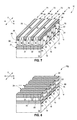
- a construction 10 comprises an electrically insulative material 12 supporting a plurality of rails 14 - 18 .
- the rails are elongated along a direction of an illustrated axis 5 in the shown embodiment, and such axis may be referred to as a first axis.
- the rails are substantially straight in the shown embodiment, in other embodiments the rails may be curved or wavy. Even if the rails are curved or wavy, such rails may extend primarily along the illustrated axis 5 in some embodiments.
- the electrically insulative material 12 may comprise any suitable composition or combination of compositions, and in some embodiments may comprise one or more of silicon nitride, silicon dioxide, and any of various doped glasses (for instance, borophosphosilicate glass, phosphosilicate glass, fluorosilicate glass, etc.).
- the insulative material 12 may be supported over a semiconductor base (not shown). Such base may comprise, for example, monocrystalline silicon. If the electrically insulative material is supported by a semiconductor base, the combination of the electrically insulative material 12 and the underlying semiconductor base may be referred to as a semiconductor substrate, or as a portion of a semiconductor substrate.
- semiconductor substrate means any construction comprising semiconductive material, including, but not limited to, bulk semiconductive materials such as a semiconductive wafer (either alone or in assemblies comprising other materials), and semiconductive material layers (either alone or in assemblies comprising other materials).
- substrate refers to any supporting structure, including, but not limited to, the semiconductor substrates described above.
- the insulative material 12 may be over a semiconductor construction which comprises a semiconductor base and one or more levels of integrated circuitry.
- the levels of integrated circuitry may comprise, for example, one or more of refractory metal materials, barrier materials, diffusion materials, insulator materials, etc.
- the rails 14 - 18 may comprise several stacked materials in some embodiments.
- the bottom material of the shown rails is an electrically conductive material 20 .
- Such electrically conductive material may comprise any suitable composition or combination of compositions; and in some embodiments may comprise, consist essentially of, or consist of one or more of various metals (for instance, tungsten, titanium, copper, etc.), metal-containing substances (for instance, metal nitride, metal silicide, metal carbide, etc.) and conductively-doped semiconductor materials (for instance, conductively-doped silicon, conductively-doped germanium, etc.).
- the electrically conductive material 20 forms electrically conductive lines 21 (only some of which are labeled) contained within the series of rails 14 - 18 .
- Such electrically conductive lines may correspond to access/sense lines; and may, for example, correspond to wordlines or bitlines in some embodiments.
- the lines 21 may be referred to as a first series of lines to distinguish them from another
- the individual rails 14 - 18 comprise one or more materials over the lines 21 .
- the materials over lines 21 are diagrammatically illustrated as regions 22 (only some of which are labeled) over the individual lines 21 .
- Uppermost portions of the regions 22 comprise electrically conductive material 24 .
- the uppermost surface of material 24 may ultimately correspond to the top of a bottom electrode of a memory cell. In other words, the uppermost surface of material 24 may be a region where a bottom electrode of a memory cell contacts memory cell material (described below); and thus material 24 may be referred to as bottom electrode contact material.
- Materials 20 and 24 may or may not comprise the same composition as one another.
- materials 20 and 24 may be the same conductive material as one another, and the intervening segment of region 22 may simply be more of the same conductive material.
- region 22 may comprise one or more materials suitable for fabrication into select devices (for instance, transistors, diodes, etc.)—with an example of such other embodiments being described below with reference to FIGS. 8-12 .
- Each of the rails 14 - 18 extends along multiple memory cell locations, with example memory cell locations 31 - 33 being labeled relative to the rail 14 .
- memory cells may be fabricated within such memory cell locations such that memory cell material of the memory cells is directly against the bottom electrode contact material 24 (as shown, for example, in FIG. 7 ).
- the rails 14 - 18 may be formed with any suitable processing.
- the various materials of the rails 14 - 18 may be formed across substrate 12 , and a patterned mask (not shown) may be formed over such materials to define locations of the rails 14 - 18 .
- a pattern may then be transferred from the mask into the materials of the rails with one or more suitable etches, and then the mask may be removed to leave the shown construction of FIG. 1 .
- the mask may comprise any suitable composition or combination of compositions.
- the mask may comprise photolithographically-patterned photoresist.
- the mask may comprise one or more materials patterned utilizing pitch-multiplication methodologies.
- FIG. 2 shows dielectric material 36 formed within such gaps.
- the dielectric material may comprise any suitable composition or combination of compositions; and in some embodiments may comprise, consist essentially of, or consist of silicon dioxide.
- the construction of FIG. 2 is shown to have a planarized surface 37 extending across rails 14 - 18 , and across the dielectric material 36 .
- Such construction may be formed by initially forming dielectric material 36 to fill the gaps between the rails 14 - 18 , and to extend across upper surfaces of the rails; and then utilizing chemical-mechanical polishing (CMP) to remove the dielectric material from over the rails and form the planarized surface 37 .
- CMP chemical-mechanical polishing
- an expanse of pad material 38 is formed across the planarized upper surface 37 , and an expanse of sacrificial material 40 is formed across the pad material.
- the pad material may comprise a sacrificial material provided as a buffer between the material 40 and the bottom electrode contact material 24 .
- the pad material may be omitted and the sacrificial material 40 may be provided directly on the bottom electrode contact material.
- the pad material may correspond to a memory cell material which is ultimately incorporated into memory cells.
- the memory cell material may be any material either now known, or yet to be developed, which is suitable for utilization in cross-point memory.
- the memory cell material may be a material suitable for utilization in one or more of PCRAM, RRAM, CBRAM, PCM, etc.
- the memory cell material may comprise an oxide containing one or more of aluminum, antimony, barium, calcium, cesium, germanium, hafnium, iron, lanthanum, lead, manganese, praseodymium, ruthenium, samarium, selenium, silicon, strontium, sulfur, tellurium, titanium, yttrium and zirconium.
- the memory cell material may comprise multivalent metal oxide; and may, for example, comprise, consist essentially of, or consist of one or more of barium, ruthenium, strontium, titanium, calcium, manganese, praseodymium, lanthanum and samarium.
- the multivalent metal oxide may comprise, consist essentially of, or consist of calcium manganese oxide doped with one or more of Pr, La, Sr and Sm.
- the memory cell material may comprise chalcogenide-type materials (for instance, materials comprising germanium in combination with one or more of antimony, tellurium, sulfur and selenium).
- the memory cell material may include additional layers, such as an ion source material suitable for contributing ions which ultimately form conductive bridges in PMC devices.
- the ion source material may comprise, for example, one or both of copper and silver; and may thus be configured for contributing copper cations and/or silver cations for formation of a conductive bridge.
- the ion source material may comprise a combination of copper and tellurium.
- the memory cell material may be a solid, gel, or any other suitable phase.
- the material 38 may be alternatively either a sacrificial material or a memory cell material in some embodiments, the material 38 may be referred to herein as a pad material, sacrificial material, or memory cell material in describing various different embodiments.
- the term “pad material” as utilized in referring to material 38 is generic relative to the terms “sacrificial material” and “memory cell material.”
- the sacrificial material 40 may comprise any suitable composition or combination of compositions; and in some embodiments may comprise, consist essentially of, or consist of silicon (for instance, may consist of one or both of amorphous silicon and polycrystalline silicon).
- the sacrificial material 40 is patterned into a series of lines 41 - 44 .
- the lines 41 - 44 may be referred to as a second series of lines to distinguish them from the first series of lines corresponding to the lines 21 contained within the rails 14 - 18 .
- the lines 41 - 44 cross the rails 14 - 18 ; and in the shown embodiment are substantially orthogonal to the rails 14 - 18 .
- the lines 41 - 44 are elongated along an axis 7
- the rails 14 - 18 are elongated along the axis 5 which is substantially orthogonal to the axis 7 .
- substantially orthogonal is utilized to indicate that the two axes are orthogonal within reasonable tolerances of design and measurement.
- the sacrificial material lines 41 - 44 are directly over the memory cell locations (for instance, the locations 31 - 33 ).
- the pattern of the sacrificial material lines 41 - 44 is transferred into the bottom electrode contact material 24 to singulate such material into segments 46 (only some of which are labeled). Each segment is associated with only a single memory cell location.
- the pattern may be transferred into the bottom electrode contact material with any suitable etch or combination of etches.
- the pattern of the sacrificial material lines is also transferred into the one or more materials beneath the bottom electrode contact material of the rails 14 - 18 .
- the singulation of regions 22 into pedestals 48 may form individual select devices.
- FIGS. 8-12 describe an embodiment in which the singulation forms individual diodes.
- the pattern may be transferred into the one or more materials of regions 22 with any suitable etch or combination of etches.
- the pedestals 48 are capped with the bottom electrode contact material 24 , and are directly between the memory cell locations (for instance, the locations 31 - 33 ) and the conductive material 20 .
- the sacrificial material 40 may be patterned into the lines 41 - 44 with any suitable processing.
- a patterned mask (not shown) may be formed over sacrificial material 40 to define locations of the lines 41 - 44 , a pattern may be transferred from the mask into material 40 with one or more suitable etches, and then the mask may be removed.
- the mask may comprise any suitable composition or combination of compositions.
- the mask may comprise photolithographically-patterned photoresist.
- the mask may comprise one or more materials patterned utilizing pitch-multiplication methodologies. The mask may remain during the patterning of the materials of regions 22 in some embodiments, and may be removed prior to such patterning in other embodiments.
- the illustrated construction 10 at the processing stage of FIG. 4 has a plurality of trenches 51 - 53 formed between the lines 41 - 44 .
- the trenches 51 - 53 extend along the same direction as the lines 41 - 44 .
- the trenches 51 - 53 may be referred to as a first series of trenches.
- dielectric material 54 is formed within the trenches 51 - 53 . Although a single dielectric material is shown, in other embodiments multiple dielectric materials may be formed within such trenches. In some embodiments, the dielectric formed within the trenches 51 - 53 may comprise one or both of silicon nitride and silicon carbide.
- the material 54 may be formed with any suitable processing, including, for example, one or more of atomic layer deposition (ALD), chemical vapor deposition (CVD) and physical vapor deposition (PVD). In some embodiments, material 54 may be formed to extend across upper surfaces of lines 41 - 44 , and may then be subjected to CMP to form the illustrated planarized upper surface 55 .
- ALD atomic layer deposition
- CVD chemical vapor deposition
- PVD physical vapor deposition
- the material 54 is deposited under conditions which leave voids 56 within trenches 51 - 53 .
- Suitable conditions for leaving such voids are conditions in which the dielectric material pinches off across the tops of the trenches before uniformly filling central regions of the trenches.
- the dielectric provided within trenches 51 - 53 have a low dielectric constant in that such can alleviate or prevent cross-talk that may otherwise occur between memory cells on opposing sides of the trenches.
- Air has a low dielectric constant, and thus it can be advantageous to have the illustrated voids remaining within the trenches after formation of dielectric material 54 within such trenches.
- the dielectric within the trenches 51 - 53 may be referred to as dielectric lines 60 - 62 .
- such dielectric lines comprise the illustrated voids 56 in combination with dielectric material 54 .
- the illustrated voids 56 may consume at least about 10 percent of the volume of the dielectric lines formed within the trenches.
- voids 56 are present in the shown embodiment, in other embodiments the dielectric 54 may be provided to entirely fill trenches 51 - 53 . Thus, the voids may be omitted.
- sacrificial material 40 ( FIG. 5 ) is removed to leave trenches 65 - 68 .
- the trenches 65 - 68 may be referred to as a second series of trenches to distinguish them from the first series of trenches 51 - 53 ( FIG. 4 ).
- the sacrificial material consists of silicon (for instance, polycrystalline silicon), such may be removed utilizing tetramethylammonium hydroxide in some embodiments.
- trenches 65 - 68 are directly over the bottom electrode contact material 24 .
- the formation of trenches 65 - 68 exposes memory cell material 38 .
- material 38 may correspond to a sacrificial pad material which is removed from over bottom electrode contact material 24 , and then replaced with memory cell material.
- material 38 may be omitted (as discussed above with reference to FIG. 3 ); and in such embodiments the memory cell material may be formed subsequent to the formation of the trenches 65 - 68 to create the shown construction of FIG. 6 .
- the memory cell material 38 in the embodiment of FIG. 6 is configured as a planar sheet. If the memory cell material is deposited after removal of sacrificial material 40 ( FIG. 5 ), the memory cell material may have a different configuration. For instance, FIG. 14 (discussed below) shows an embodiment in which memory cell material is configured as upwardly-opening container structures.
- the one or more memory cell materials may be any materials suitable for forming cross-point memory cells, either now known or later developed.
- the memory cell materials may be suitable for utilization in one or more of PCRAM, RRAM, CBRAM, PCM, etc.
- top electrode material 70 is formed within the trenches 65 - 68 .
- the top electrode material may comprise any suitable composition or combination of compositions, and in some embodiments may comprise, consist essentially of, or consist of one or more of platinum, silver and copper. Accordingly, the top electrode material may comprise, consist essentially of, or consist of one or more noble metals. As discussed above in the “background” section of this disclosure, it can be difficult to pattern noble metals.
- the trenches 65 - 68 enable utilization of a damascene process for patterning the electrode material 70 .
- top electrode material 70 may be formed to fill trenches 65 - 68 and to extend over dielectric lines 60 - 62 .
- the top electrode material may then be planarized (for instance, subjected to CMP) to remove the top electrode material 70 from over the dielectric material lines and thereby form the illustrated top electrode lines 71 - 74 .
- Such top electrode lines extend along the axis 7 , and thus cross the bottom electrode lines 21 .
- the top electrode material 70 may comprise copper.
- dielectric 54 it may be desired for dielectric 54 to comprise copper barrier material, such as one or more nitrides and/or it may be desired for the conductive top electrode material to be surrounded by electrically conductive barrier material.
- Memory cells 76 are formed in the memory cell locations (for instance, the locations 31 - 33 ), with such memory cells having memory cell material 38 directly between the bottom electrode contact material 24 and the electrode material 70 .
- the memory cells may be considered to be configured as a memory array.
- the formation of the top electrode lines 71 - 74 may be considered to be replacement of at least some of the sacrificial material 40 of lines 41 - 44 ( FIG. 5 ) with top electrode material 70 .
- all of the sacrificial material 40 of lines 41 - 44 is replaced with electrode material 70 .
- memory cell material may be formed within trenches 65 - 68 prior to formation of the electrode material 70 ; and in such embodiments a portion of the sacrificial material 40 of lines 41 - 44 may be considered to be replaced with the memory cell material, and another portion of the sacrificial material 40 of lines 41 - 44 may be considered to be replaced with the electrode material 70 .
- the materials of region 22 may correspond to materials suitable for forming select devices.
- Example select devices are transistors (for instance, vertical transistors) and diodes.
- FIGS. 8-12 illustrate an example embodiment in which region 22 comprises materials suitable for fabrication into diodes.
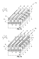
- a construction 10 a is shown at a processing stage analogous to that of FIG. 1 .
- the rails 14 - 18 comprise stacks of materials 20 , 78 and 80 .
- Such materials may correspond to suitable compositions for a diode construction.
- materials 20 , 78 and 80 may be suitable compositions for a metal-silicon-metal diode (specifically, materials 20 and 80 may be metal, and material 78 may be silicon), or may be suitable compositions for a PIN diode (specifically, region 78 may be intrinsic semiconductor material, one of the regions 20 and 80 may be n-type doped semiconductor material, and the other of the regions 20 and 80 may be p-type doped semiconductor material).
- the bottom electrode contact material 24 is shown to correspond to a top surface of material 80 .
- the bottom electrode contact material may be a separate conductive material from the material 80 of the diode compositions rather than being the shown top surface of material 80 .
- conductive line 20 is shown to also be one of the diode compositions, in other embodiments the line may be a separate conductive material from the bottom diode composition.
- the diode compositions 20 , 78 and 80 extend along the memory cell locations (for instance, the locations 31 - 33 ).
- construction 10 a is shown at a processing stage analogous to the above-discussed processing stage of FIG. 4 . Accordingly, the pad material 38 and sacrificial material 40 have been formed over rails 14 - 18 , and then the construction has been subjected to patterning to form the lines 41 - 44 and the trenches 51 - 53 .
- the formation of the trenches singulates diodes 82 (only some of which are labeled) from the diode compositions 20 , 78 and 80 . Specifically, the trenches extend through materials 78 and 80 to form individual diodes under individual memory cell locations (for instance, the memory cell locations 31 - 33 ). In embodiments in which the bottom diode composition is a different conductive material from the material of the conductive line 20 , the trenches may extend through the bottom diode composition in addition to extending through the diode compositions 78 and 80 .
- construction 10 a is shown at a processing stage analogous to the above-discussed processing stage of FIG. 5 .
- the construction comprises the dielectric lines 60 - 62 within the trenches 51 - 53 .
- Such dielectric lines comprise the voids 56 in combination with the dielectric material 54 in the shown embodiment.
- the construction 10 a also comprises the planarized upper surface 55 .
- construction 10 a is shown at a processing stage analogous to that discussed above with reference to FIG. 6 .
- the sacrificial material 40 ( FIG. 10 ) has been removed to leave the trenches 65 - 68 between the dielectric lines 60 - 62 .
- the material 38 is at the bottoms of the trenches 65 - 68 , and corresponds to memory cell material of the type described above with reference to FIG. 6 .
- the material 38 may be sacrificial material which is removed and replaced with memory cell material, as discussed above with reference to FIG. 6 .
- construction 10 a is shown at a processing stage analogous to that discussed above with reference to FIG. 7 .
- Top electrode material 70 has been formed within the trenches 65 - 68 and patterned to form the top electrode lines 71 - 74 .
- Memory cells 76 are formed in the memory cell locations (for instance, the locations 31 - 33 ), with such memory cells having memory cell material 38 directly between the bottom electrode contact material 24 and the electrode material 70 . Each memory cell is directly over one of the diodes 82 .
- FIGS. 8-12 singulates the diodes 82 during patterning of the memory cell material 38 , which consolidates process steps relative to prior art processing. Such may improve throughput of a fabrication process relative to prior art processes, and may eliminate masking steps relative to prior art processes.
- FIGS. 13 and 14 illustrate another example embodiment method.
- FIG. 13 a construction 10 b is shown at a processing stage analogous to that described above with reference to FIG. 6 .
- the embodiment of FIG. 13 does not have such pad material at the bottoms of such trenches.
- memory cell material 90 is formed within the trenches 65 - 68 to line such trenches.
- the memory cell material forms upwardly-opening container structures within the trenches.
- top electrode material 70 is formed within such upwardly-opening container structures and patterned to form the top electrode lines 71 - 74 .
- the memory cell material 90 may be formed as a planar structure rather than as the container-shaped structure of FIG. 14 .
- FIG. 15 shows a construction 10 c at a processing stage analogous to that of FIG. 14 , but in which the memory cell material 90 has been formed as a planar structure.
- multiple memory cell materials may be utilized in the memory cells.
- the memory cell materials may have different shapes relative to one another.
- FIG. 16 shows a construction 10 d utilizing two different memory cell materials 92 and 94 .
- the memory cell material 92 is configured as a planar structure
- the memory cell material 94 is configured as a container-shaped structure provided directly over and directly against the memory cell material 92 .
- the memory cell materials 92 and 94 may be referred to as first and second memory cell materials, respectively.
- the memory cell material 92 may correspond to the pad material 38 of FIG. 6 , and the material 94 may be provided within trenches 65 - 68 prior to forming the top electrode material 70 of FIG. 7 . In other embodiments, the memory cell materials 92 and 94 may both be formed within trenches 65 - 68 following a process stage analogous to that of FIG. 13 so that neither of the memory cell materials corresponds to the pad material 38 of FIG. 6 .
- the utilization of two memory cell materials may be useful in, for example, forming PCM cells in which one of the memory cell materials is an ion source (for instance, a combination of copper and tellurium) and the other is a switching region (for instance, an oxide or solid state electrolyte); forming RRAM cells in which one of the memory cell materials is a multivalent oxide and the other is a high k dielectric; etc.
- ion source for instance, a combination of copper and tellurium
- a switching region for instance, an oxide or solid state electrolyte
- RRAM cells in which one of the memory cell materials is a multivalent oxide and the other is a high k dielectric
- more than two memory cell materials may be utilized.
- a construction analogous to that of FIG. 16 may be configured to have the electrode material 70 comprise copper, and the container-shaped material 94 may comprise a copper barrier material (such as a nitride). In such embodiments, the material 94 may or may not be a memory cell material.
- FIGS. 17-23 illustrate another example embodiment method of fabricating an array of memory cells.
- a construction 10 e is shown at a processing stage analogous to that of FIG. 1 .
- the rails 14 - 18 include memory cell material 38 and an electrically conductive material 100 .
- the material 100 may comprise any suitable composition or combination of compositions, and in some embodiments may comprise one or more of various metals (for instance, tungsten, platinum, silver, copper, etc.), metal-containing compositions (for instance, metal silicide, metal carbide, etc.) and conductively-doped semiconductor materials (for instance, conductively-doped silicon, conductively-doped germanium, etc.).
- metals for instance, tungsten, platinum, silver, copper, etc.
- metal-containing compositions for instance, metal silicide, metal carbide, etc.
- conductively-doped semiconductor materials for instance, conductively-doped silicon, conductively-doped germanium, etc.
- FIGS. 18-23 show the construction 10 e processed with methodology analogous to that discussed above with reference to FIGS. 2-7 to form an array of memory cells (with such array comprising the illustrated memory cells 31 - 33 in FIG. 23 ).
- the memory cell material 38 of FIGS. 17-23 is singulated during the singulation of conductive material 24 .
- each of the memory cells in the memory array of FIG. 23 (for instance, the memory cells 31 - 33 ) comprises a segment of material 38 , with each segment of material 38 being associated with only a single memory cell location.
- the memory cell material 38 within the memory array of FIG. 7 is shown to be patterned into expanses which extended across multiple memory cells.
- the conductive material 100 is patterned together with the memory cell material 38 to form segments of material 100 in one-to-one correspondence with the memory cells (for instance, the memory cells 31 - 33 ).
- region 22 may correspond to materials suitable for forming select devices.
- Example select devices are transistors (for instance, vertical transistors) and diodes.
- FIG. 24 illustrates an example embodiment in which region 22 comprises materials suitable for fabrication into diodes. Specifically, FIG. 24 shows a construction 10 f at a processing stage analogous to that of FIG. 12 , with construction 10 f comprising the singulated memory cell material 38 and conductive material 100 discussed above with reference to FIGS. 17-23 .
- the regions 20 , 78 and 80 may be regions of a diode (for instance, region 20 may be an n-type doped region, region 78 may be an intrinsic region, and region 80 may be a p-type doped region, as discussed above with reference to FIGS. 8-12 ).
- the memory cells 76 also comprise a conductive material 102 between the top diode region 80 and the memory cell material 38 . Such conductive material may be utilized to improve adhesion between of material 38 , improve electrical transfer to material 38 and/or to improve other properties of the memory cells.
- the conductive material 102 may comprise any suitable composition or combination of compositions and in some embodiments may comprise one or more of various metals (for instance, tungsten, platinum, silver, copper, etc.), metal-containing compositions (for instance, metal silicide, metal carbide, etc.) and conductively-doped semiconductor materials (for instance, conductively-doped silicon, conductively-doped germanium, etc.).
- the materials 100 and 102 are shown to have different thicknesses relative to one another, with material 100 being thicker than material 102 . In other embodiments, materials 100 and 102 may be about the same thickness as one another, or material 102 may be thicker than material 100 .
- the memory cells and arrays discussed above may be incorporated into electronic systems.
- Such electronic systems may be any of a broad range of systems either now known or yet to be developed; with example electronic systems being clocks, televisions, cell phones, personal computers, automobiles, industrial control systems, aircraft, etc.
- Some embodiments include a method of forming a plurality of memory cells.
- a series of rails is formed to extend along a first direction. Individual rails extend along multiple memory cell locations.
- the individual rails comprise bottom electrode contact material over electrically conductive lines.
- the electrically conductive lines are a first series of lines.
- An expanse of sacrificial material is formed to extend across the rails.
- the sacrificial material is patterned into a second series of lines that extends along a second direction that crosses the first direction.
- a pattern of the second series of lines is transferred into the bottom electrode contact material to singulate the bottom electrode contact material into segments associated with only single memory cell locations. At least a portion of the sacrificial material of the second series of lines is replaced with top electrode material.
- Some embodiments include a method of forming a plurality of memory cells.
- a series of rails is formed to extend along a first direction. Individual rails extend along multiple memory cell locations. The individual rails comprise bottom electrode contact material stacked over electrically conductive lines.
- a series of sacrificial material lines is formed to extend along a second direction that crosses the first direction. The sacrificial material lines are directly over the memory cell locations. A pattern of the sacrificial material lines is transferred into the bottom electrode contact material to singulate the bottom electrode contact material into segments associated with only single memory cell locations.
- a series of dielectric lines is formed between the sacrificial material lines. The dielectric lines extend along the second direction. The sacrificial material lines are removed to leave trenches between the dielectric lines.
- top electrode material is formed within the trenches and over the dielectric material lines.
- the top electrode material is planarized to remove the top electrode material from over the dielectric material lines and thereby form a plurality of top electrode lines directly over the memory cell locations.
- the top electrode lines extend along the second direction.
- Some embodiments include a method of forming a plurality of memory cells.
- a series of rails is formed to extend along a first direction. Individual rails extend along multiple memory cell locations.
- the individual rails comprise bottom electrode contact material stacked over electrically conductive lines.
- the electrically conductive lines are a first series of lines.
- An expanse of sacrificial material is formed to extend across the rails.
- the sacrificial material is patterned into a second series of lines which extend along a second direction that crosses the first direction.
- a pattern of the second series of lines is transferred into the bottom electrode contact material to singulate the bottom electrode contact material into segments associated with only single memory cell locations. The transferring of the pattern forms a series of first trenches that extend along the second direction.
- Individual trenches of the first series are between adjacent lines of the second series.
- One or more dielectric materials are formed within the first series of trenches. After said one or more dielectric materials are formed, the sacrificial material is removed to leave a second series of trenches that extend along the second direction. Individual trenches of the second series are directly over the segments of bottom electrode contact material.
- Top electrode material is formed within the second series of trenches and over the one or more dielectric materials. The top electrode material is planarized to remove the top electrode material from over the one or more dielectric materials and thereby form a plurality of top electrode lines that extend along the second direction.
- Some embodiments include a memory array that comprises a first series of electrically conductive lines extending along a first direction. Pillars are over the first series of electrically conductive lines. The pillars are capped with bottom electrode contact material and are directly between the electrically conductive lines of the first series and memory cell locations. One or more memory cell materials are over the pillars and within the memory cell locations. A second series of electrically conductive lines extends along a second direction that crosses the first direction. The second series of electrically conductive lines comprises top electrode material. The memory cell locations are directly between the electrically conductive lines of the first and second series, and are in regions where the electrically conductive lines of the second series overlap the electrically conductive lines of the first series. The electrically conductive lines of the second series comprise one or more of platinum, copper and silver.
- Some embodiments include a memory array that comprises a first series of electrically conductive lines extending along a first direction. Pillars are over the first series of electrically conductive lines. The pillars are capped with bottom electrode contact material and are directly between the electrically conductive lines of the first series and memory cell locations. A first memory cell material is over the pillars and within the memory cell locations. The first memory cell material is a planar sheet within the memory cell locations, and is directly against the bottom electrode contact material. A second memory cell material is over the first memory cell material. The second memory cell material is configured as a plurality of upwardly-opening containers that extend linearly along a second direction that crosses the first direction. A second series of electrically conductive lines is within the containers. The second series of electrically conductive lines comprises top electrode material. The memory cell locations are directly between the electrically conductive lines of the first and second series, and are in regions where the electrically conductive lines of the second series overlap the electrically conductive lines of the first series.
Landscapes
- Semiconductor Memories (AREA)
Abstract
Description
Claims (17)
Priority Applications (1)
| Application Number | Priority Date | Filing Date | Title |
|---|---|---|---|
| US15/857,448 US10069067B2 (en) | 2011-11-17 | 2017-12-28 | Memory arrays and methods of forming memory cells |
Applications Claiming Priority (3)
| Application Number | Priority Date | Filing Date | Title |
|---|---|---|---|
| US13/298,840 US9252188B2 (en) | 2011-11-17 | 2011-11-17 | Methods of forming memory cells |
| US15/003,715 US9893277B2 (en) | 2011-11-17 | 2016-01-21 | Memory arrays and methods of forming memory cells |
| US15/857,448 US10069067B2 (en) | 2011-11-17 | 2017-12-28 | Memory arrays and methods of forming memory cells |
Related Parent Applications (1)
| Application Number | Title | Priority Date | Filing Date |
|---|---|---|---|
| US15/003,715 Continuation US9893277B2 (en) | 2011-11-17 | 2016-01-21 | Memory arrays and methods of forming memory cells |
Publications (2)
| Publication Number | Publication Date |
|---|---|
| US20180123035A1 US20180123035A1 (en) | 2018-05-03 |
| US10069067B2 true US10069067B2 (en) | 2018-09-04 |
Family
ID=48425920
Family Applications (3)
| Application Number | Title | Priority Date | Filing Date |
|---|---|---|---|
| US13/298,840 Active 2032-09-13 US9252188B2 (en) | 2011-11-17 | 2011-11-17 | Methods of forming memory cells |
| US15/003,715 Active US9893277B2 (en) | 2011-11-17 | 2016-01-21 | Memory arrays and methods of forming memory cells |
| US15/857,448 Active US10069067B2 (en) | 2011-11-17 | 2017-12-28 | Memory arrays and methods of forming memory cells |
Family Applications Before (2)
| Application Number | Title | Priority Date | Filing Date |
|---|---|---|---|
| US13/298,840 Active 2032-09-13 US9252188B2 (en) | 2011-11-17 | 2011-11-17 | Methods of forming memory cells |
| US15/003,715 Active US9893277B2 (en) | 2011-11-17 | 2016-01-21 | Memory arrays and methods of forming memory cells |
Country Status (1)
| Country | Link |
|---|---|
| US (3) | US9252188B2 (en) |
Families Citing this family (49)
| Publication number | Priority date | Publication date | Assignee | Title |
|---|---|---|---|---|
| US9454997B2 (en) | 2010-12-02 | 2016-09-27 | Micron Technology, Inc. | Array of nonvolatile memory cells having at least five memory cells per unit cell, having a plurality of the unit cells which individually comprise three elevational regions of programmable material, and/or having a continuous volume having a combination of a plurality of vertically oriented memory cells and a plurality of horizontally oriented memory cells; array of vertically stacked tiers of nonvolatile memory cells |
| US8486743B2 (en) | 2011-03-23 | 2013-07-16 | Micron Technology, Inc. | Methods of forming memory cells |
| US8994489B2 (en) | 2011-10-19 | 2015-03-31 | Micron Technology, Inc. | Fuses, and methods of forming and using fuses |
| US8723155B2 (en) | 2011-11-17 | 2014-05-13 | Micron Technology, Inc. | Memory cells and integrated devices |
| US9252188B2 (en) | 2011-11-17 | 2016-02-02 | Micron Technology, Inc. | Methods of forming memory cells |
| US8546231B2 (en) | 2011-11-17 | 2013-10-01 | Micron Technology, Inc. | Memory arrays and methods of forming memory cells |
| US8759807B2 (en) | 2012-03-22 | 2014-06-24 | Micron Technology, Inc. | Memory cells |
| US9136467B2 (en) | 2012-04-30 | 2015-09-15 | Micron Technology, Inc. | Phase change memory cells and methods of forming phase change memory cells |
| US9627611B2 (en) | 2012-11-21 | 2017-04-18 | Micron Technology, Inc. | Methods for forming narrow vertical pillars and integrated circuit devices having the same |
| US9337293B2 (en) * | 2013-02-22 | 2016-05-10 | Taiwan Semiconductor Manufacturing Company, Ltd. | Semiconductor device having electrode and manufacturing method thereof |
| KR20140127576A (en) * | 2013-04-25 | 2014-11-04 | 에스케이하이닉스 주식회사 | Resistive Memory Device and Fabrication Method Thereof |
| US9337210B2 (en) | 2013-08-12 | 2016-05-10 | Micron Technology, Inc. | Vertical ferroelectric field effect transistor constructions, constructions comprising a pair of vertical ferroelectric field effect transistors, vertical strings of ferroelectric field effect transistors, and vertical strings of laterally opposing pairs of vertical ferroelectric field effect transistors |
| CN103682094B (en) * | 2013-12-11 | 2016-08-17 | 上海新安纳电子科技有限公司 | A kind of phase change memory structure and preparation method thereof |
| US9041217B1 (en) * | 2013-12-18 | 2015-05-26 | Intel Corporation | Self-aligned via patterning with multi-colored photobuckets for back end of line (BEOL) interconnects |
| US9276134B2 (en) | 2014-01-10 | 2016-03-01 | Micron Technology, Inc. | Field effect transistor constructions and memory arrays |
| KR20150090472A (en) | 2014-01-29 | 2015-08-06 | 삼성전자주식회사 | Variable resistance memory devices and methods of manufacturing the same |
| US9685607B2 (en) * | 2014-03-11 | 2017-06-20 | Kabushiki Kaisha Toshiba | Non-volatile semiconductor memory device |
| US9306165B2 (en) * | 2014-03-27 | 2016-04-05 | Micron Technology, Inc. | Replacement materials processes for forming cross point memory |
| US9881971B2 (en) | 2014-04-01 | 2018-01-30 | Micron Technology, Inc. | Memory arrays |
| US9263577B2 (en) | 2014-04-24 | 2016-02-16 | Micron Technology, Inc. | Ferroelectric field effect transistors, pluralities of ferroelectric field effect transistors arrayed in row lines and column lines, and methods of forming a plurality of ferroelectric field effect transistors |
| US9362494B2 (en) | 2014-06-02 | 2016-06-07 | Micron Technology, Inc. | Array of cross point memory cells and methods of forming an array of cross point memory cells |
| US9343506B2 (en) | 2014-06-04 | 2016-05-17 | Micron Technology, Inc. | Memory arrays with polygonal memory cells having specific sidewall orientations |
| US9472560B2 (en) | 2014-06-16 | 2016-10-18 | Micron Technology, Inc. | Memory cell and an array of memory cells |
| US9728721B2 (en) | 2014-07-25 | 2017-08-08 | Globalfoundries Singapore Pte. Ltd. | Resistive memory device |
| US9263325B1 (en) * | 2014-08-20 | 2016-02-16 | Globalfoundries Inc. | Precut metal lines |
| US9159829B1 (en) | 2014-10-07 | 2015-10-13 | Micron Technology, Inc. | Recessed transistors containing ferroelectric material |
| US9276092B1 (en) | 2014-10-16 | 2016-03-01 | Micron Technology, Inc. | Transistors and methods of forming transistors |
| US9748311B2 (en) * | 2014-11-07 | 2017-08-29 | Micron Technology, Inc. | Cross-point memory and methods for fabrication of same |
| US9502293B2 (en) * | 2014-11-18 | 2016-11-22 | Globalfoundries Inc. | Self-aligned via process flow |
| US9305929B1 (en) | 2015-02-17 | 2016-04-05 | Micron Technology, Inc. | Memory cells |
| KR20160124579A (en) * | 2015-04-20 | 2016-10-28 | 에스케이하이닉스 주식회사 | Semiconductor device having air gap and method for manufacturing the same, memory cell having the same and electronic device having the same |
| US9853211B2 (en) * | 2015-07-24 | 2017-12-26 | Micron Technology, Inc. | Array of cross point memory cells individually comprising a select device and a programmable device |
| US10134982B2 (en) | 2015-07-24 | 2018-11-20 | Micron Technology, Inc. | Array of cross point memory cells |
| CN105405972B (en) * | 2015-12-15 | 2019-06-25 | 上海新储集成电路有限公司 | Retain the preparation method of the three-dimensional resistance-variable storing device of air layer |
| WO2017111924A1 (en) * | 2015-12-21 | 2017-06-29 | Intel Corporation | Grating based plugs and cuts for feature end formation for back end of line (beol) interconnects and structures resulting therefrom |
| US10396145B2 (en) | 2017-01-12 | 2019-08-27 | Micron Technology, Inc. | Memory cells comprising ferroelectric material and including current leakage paths having different total resistances |
| US10153196B1 (en) | 2017-08-24 | 2018-12-11 | Micron Technology, Inc. | Arrays of cross-point memory structures |
| US10312438B1 (en) * | 2017-12-18 | 2019-06-04 | International Business Machines Corporation | Resistive memory with amorphous silicon filaments |
| CN110277389B (en) * | 2018-03-14 | 2021-10-08 | 联华电子股份有限公司 | Semiconductor structure with conductive line and method of making stop layer |
| US10505111B1 (en) * | 2018-07-20 | 2019-12-10 | International Business Machines Corporation | Confined phase change memory with double air gap |
| US10833092B2 (en) | 2019-01-23 | 2020-11-10 | Micron Technology, Inc. | Methods of incorporating leaker-devices into capacitor configurations to reduce cell disturb, and capacitor configurations incorporating leaker-devices |
| US10832941B2 (en) | 2019-03-27 | 2020-11-10 | International Business Machines Corporation | Airgap isolation for backend embedded memory stack pillar arrays |
| US11018188B2 (en) | 2019-06-03 | 2021-05-25 | International Business Machines Corporation | Three-dimensional stackable multi-layer cross-point memory with bipolar junction transistor selectors |
| US10903275B2 (en) | 2019-06-03 | 2021-01-26 | International Business Machines Corporation | Three-dimensional stackable multi-layer cross-point memory with single-crystalline bipolar junction transistor selectors |
| US11170834B2 (en) | 2019-07-10 | 2021-11-09 | Micron Technology, Inc. | Memory cells and methods of forming a capacitor including current leakage paths having different total resistances |
| US11417841B2 (en) * | 2019-08-13 | 2022-08-16 | Micron Technology, Inc. | Techniques for forming self-aligned memory structures |
| US11139202B2 (en) * | 2019-09-27 | 2021-10-05 | International Business Machines Corporation | Fully aligned top vias with replacement metal lines |
| US11424118B2 (en) * | 2020-01-23 | 2022-08-23 | Micron Technology, Inc. | Electronic devices comprising silicon carbide materials |
| CN112420729B (en) * | 2020-11-06 | 2021-11-16 | 长江存储科技有限责任公司 | 3D memory device and method of manufacturing the same |
Citations (174)
| Publication number | Priority date | Publication date | Assignee | Title |
|---|---|---|---|---|
| US4080719A (en) | 1975-09-17 | 1978-03-28 | U.S. Philips Corporation | Method of manufacturing a semiconductor device and device manufactured according to the method |
| US4499557A (en) | 1980-10-28 | 1985-02-12 | Energy Conversion Devices, Inc. | Programmable cell for use in programmable electronic arrays |
| US4752118A (en) | 1985-03-08 | 1988-06-21 | Energy Conversion Devices, Inc. | Electric circuits having repairable circuit lines and method of making the same |
| US4849247A (en) | 1987-12-14 | 1989-07-18 | Sundstrand Corporation | Enhanced adhesion of substrate materials using ion-beam implantation |
| US4987099A (en) | 1989-12-29 | 1991-01-22 | North American Philips Corp. | Method for selectively filling contacts or vias or various depths with CVD tungsten |
| US5055423A (en) | 1987-12-28 | 1991-10-08 | Texas Instruments Incorporated | Planarized selective tungsten metallization system |
| US5166758A (en) | 1991-01-18 | 1992-11-24 | Energy Conversion Devices, Inc. | Electrically erasable phase change memory |
| US5168332A (en) | 1989-11-27 | 1992-12-01 | Kabushiki Kaisha Toshiba | Semiconductor device having salicide structure, method of manufacturing the same, and heating apparatus |
| US5341328A (en) | 1991-01-18 | 1994-08-23 | Energy Conversion Devices, Inc. | Electrically erasable memory elements having reduced switching current requirements and increased write/erase cycle life |
| US5895963A (en) | 1997-02-07 | 1999-04-20 | Nec Corporation | Semiconductor device having opening portion for fuse breakage |
| US5912839A (en) | 1998-06-23 | 1999-06-15 | Energy Conversion Devices, Inc. | Universal memory element and method of programming same |
| US6143670A (en) | 1998-12-28 | 2000-11-07 | Taiwan Semiconductor Manufacturing Company | Method to improve adhesion between low dielectric constant layer and silicon containing dielectric layer |
| US20020017701A1 (en) | 1999-03-25 | 2002-02-14 | Patrick Klersy | Electrically programmable memory element with raised pore |
| US20020173101A1 (en) | 2000-01-11 | 2002-11-21 | Jeng-Jye Shau | Embedded electrically programmable read only memory devices |
| US20020177292A1 (en) | 2000-12-26 | 2002-11-28 | Charles Dennison | Method for forming phase-change memory bipolar array utilizing a single shallow trench isolation for creating an individual active area region for two memory array elements and one bipolar base contact |
| US6611453B2 (en) | 2001-01-24 | 2003-08-26 | Infineon Technologies Ag | Self-aligned cross-point MRAM device with aluminum metallization layers |
| US6613604B2 (en) | 2001-08-02 | 2003-09-02 | Ovonyx, Inc. | Method for making small pore for use in programmable resistance memory element |
| US6661330B1 (en) | 2002-07-23 | 2003-12-09 | Texas Instruments Incorporated | Electrical fuse for semiconductor integrated circuits |
| US6664182B2 (en) | 2001-04-25 | 2003-12-16 | Macronix International Co. Ltd. | Method of improving the interlayer adhesion property of low-k layers in a dual damascene process |
| US6692898B2 (en) | 2001-01-24 | 2004-02-17 | Infineon Technologies Ag | Self-aligned conductive line for cross-point magnetic memory integrated circuits |
| US6700211B2 (en) | 1996-02-23 | 2004-03-02 | Micron Technology, Inc. | Method for forming conductors in semiconductor devices |
| US6764894B2 (en) | 2001-08-31 | 2004-07-20 | Ovonyx, Inc. | Elevated pore phase-change memory |
| US20040178425A1 (en) | 2003-03-14 | 2004-09-16 | Renesas Technology Corp. | Semiconductor device having fuse |
| US20040188668A1 (en) | 2003-03-31 | 2004-09-30 | International Business Machines Corporation | Thermal memory cell and memory device including the thermal memory cell |
| US20040195604A1 (en) | 2003-04-02 | 2004-10-07 | Young-Nam Hwang | Phase-change memory devices and methods for forming the same |
| US6815704B1 (en) | 2003-09-04 | 2004-11-09 | Silicon Storage Technology, Inc. | Phase change memory device employing thermally insulating voids |
| US20050001212A1 (en) | 2003-04-23 | 2005-01-06 | Hitachi, Ltd. | Semiconductor device and manufacturing method thereof |
| US20050006681A1 (en) | 2003-07-09 | 2005-01-13 | Matsushita Electric Industrial Co., Ltd. | Semiconductor memory device and method for fabricating the same |
| WO2005041196A1 (en) | 2003-10-23 | 2005-05-06 | Rheinisch-Westfälische Technische Hochschule Aachen | Phase change memory, phase change memory assembly, phase change memory cell, 2d phase change memory cell array, 3d phase change memory cell array and electronic component |
| US20050110983A1 (en) | 2003-11-24 | 2005-05-26 | Won-Cheol Jeong | Phase change memory devices with contact surface area to a phase changeable material defined by a sidewall of an electrode hole and methods of forming the same |
| US20050117397A1 (en) | 2003-06-25 | 2005-06-02 | Kiyoshi Morimoto | Method of driving a non-volatile memory |
| US6906940B1 (en) | 2004-02-12 | 2005-06-14 | Macronix International Co., Ltd. | Plane decoding method and device for three dimensional memories |
| US20050162881A1 (en) | 2004-01-27 | 2005-07-28 | James Stasiak | Nanometer-scale memory device utilizing self-aligned rectifying elements and method of making |
| US20050243596A1 (en) | 2004-04-17 | 2005-11-03 | Ralf Symanczyk | Memory cell for storing an information item, memory circuit and method for producing a memory cell |
| US20060073652A1 (en) | 2004-09-17 | 2006-04-06 | Fabio Pellizzer | Phase change memory with ovonic threshold switch |
| US20060073631A1 (en) | 2004-09-24 | 2006-04-06 | Karpov Ilya V | Phase change memory with damascene memory element |
| US20060076548A1 (en) | 2004-10-08 | 2006-04-13 | Samsung Electronics Co., Ltd. | PRAMs having a plurality of active regions located vertically in sequence and methods of forming the same |
| US20060110888A1 (en) | 2004-10-19 | 2006-05-25 | Byeong-Ok Cho | Phase changeable memory device and method of formation thereof |
| US20060113520A1 (en) | 2004-12-01 | 2006-06-01 | Renesas Technology Corp. | Semiconductor integrated circuit device and method of manufacturing the same |
| US20060157679A1 (en) | 2005-01-19 | 2006-07-20 | Matrix Semiconductor, Inc. | Structure and method for biasing phase change memory array for reliable writing |
| US20060157682A1 (en) | 2005-01-19 | 2006-07-20 | Matrix Semiconductor, Inc. | Write-once nonvolatile phase change memory array |
| US20060186440A1 (en) | 2005-02-23 | 2006-08-24 | Taiwan Semiconductor Manufacturing Company, Ltd. | Phase change memory device and method of manufacture thereof |
| US20060226409A1 (en) | 2005-04-06 | 2006-10-12 | International Business Machines Corporation | Structure for confining the switching current in phase memory (PCM) cells |
| US7148140B2 (en) | 2004-07-28 | 2006-12-12 | Texas Instruments Incorporated | Partial plate anneal plate process for deposition of conductive fill material |
| US20060284279A1 (en) | 2005-06-17 | 2006-12-21 | Macronix International Co., Ltd. | Thin film fuse phase change RAM and manufacturing method |
| US20060286709A1 (en) | 2005-06-17 | 2006-12-21 | Macronix International Co., Ltd. | Manufacturing methods for thin film fuse phase change ram |
| US20070008773A1 (en) | 2005-07-11 | 2007-01-11 | Matrix Semiconductor, Inc. | Nonvolatile memory cell comprising switchable resistor and transistor |
| US20070012905A1 (en) | 2005-07-13 | 2007-01-18 | Taiwan Semiconductor Manufacturing Company, Ltd. | Novel phase change random access memory |
| US7169624B2 (en) | 2001-06-28 | 2007-01-30 | Sharp Laboratories Of America, Inc. | Shared bit line cross-point memory array manufacturing method |
| US20070029676A1 (en) | 2005-08-02 | 2007-02-08 | Norikatsu Takaura | Semiconductor device and method for manufacturing the same |
| US20070054486A1 (en) | 2005-09-05 | 2007-03-08 | Ta-Hung Yang | Method for forming opening |
| US20070075347A1 (en) | 2005-03-11 | 2007-04-05 | Li-Shyue Lai | Phase change memory devices with reduced programming current |
| US20070075359A1 (en) | 2005-10-05 | 2007-04-05 | Samsung Electronics Co., Ltd. | Circuit device including vertical transistors connected to buried bitlines and method of manufacturing the same |
| US20070108431A1 (en) | 2005-11-15 | 2007-05-17 | Chen Shih H | I-shaped phase change memory cell |
| US20070158698A1 (en) | 2005-12-23 | 2007-07-12 | Stmicroelectronics S.R.L. | Process for manufacturing a phase change selection device with reduced current leakage, and phase change selection device, in particular for phase change memory devices |
| US20070224726A1 (en) | 2005-06-17 | 2007-09-27 | Macronix International Co., Ltd. | Thin film plate phase change ram circuit and manufacturing method |
| US20070235708A1 (en) | 2006-03-30 | 2007-10-11 | International Business Machines Corporation | Programmable via structure for three dimensional integration technology |
| US20070272913A1 (en) | 2005-01-19 | 2007-11-29 | Scheuerlein Roy E | Forming nonvolatile phase change memory cell having a reduced thermal contact area |
| US20070279974A1 (en) | 2006-06-06 | 2007-12-06 | Dennison Charles H | Forming heaters for phase change memories with select devices |
| US20070285969A1 (en) | 2003-03-18 | 2007-12-13 | Kabushiki Kaisha Toshiba | Resistance change memory device |
| US20080014733A1 (en) | 2006-07-14 | 2008-01-17 | Micron Technology, Inc. | Bottom electrode contacts for semiconductor devices and methods of forming same |
| US20080017842A1 (en) | 2006-07-20 | 2008-01-24 | Thomas Happ | Phase change memory cell including nanocomposite insulator |
| US7332401B2 (en) | 2001-11-19 | 2008-02-19 | Micron Technology, Ing. | Method of fabricating an electrode structure for use in an integrated circuit |
| US20080043520A1 (en) | 2006-02-07 | 2008-02-21 | Chen Shih H | I-shaped phase change memory cell with thermal isolation |
| US20080054470A1 (en) | 2004-06-24 | 2008-03-06 | Mari Amano | Semiconductor Device and Method of Fabricating the Same |
| US20080064200A1 (en) | 2002-12-13 | 2008-03-13 | Johnson Brian G | Method to manufacture a phase change memory |
| US20080067486A1 (en) | 2005-09-14 | 2008-03-20 | Stmicroelectronics S.R.L. | Ring heater for a phase change memory device |
| US20080067485A1 (en) | 2004-10-14 | 2008-03-20 | Paola Besana | Increasing adherence of dielectrics to phase change materials |
| US20080093703A1 (en) | 2006-10-19 | 2008-04-24 | International Business Machines Corporation | Electrical fuse and method of making |
| US20080123394A1 (en) | 2006-11-09 | 2008-05-29 | Samsung Electronics Co., Ltd. | Nonvolatile memory devices using variable resistors as storage elements and methods of operating the same |
| US20080128677A1 (en) | 2006-11-30 | 2008-06-05 | Samsung Electronics Co., Ltd. | Storage node including diffusion barrier layer, phase change memory device having the same and methods of manufacturing the same |
| US20080138929A1 (en) | 2006-12-06 | 2008-06-12 | Macronix International Co., Ltd. | Method for Making a Self-Converged Memory Material Element for Memory Cell |
| US20080137400A1 (en) | 2006-12-06 | 2008-06-12 | Macronix International Co., Ltd. | Phase Change Memory Cell with Thermal Barrier and Method for Fabricating the Same |
| US20080157053A1 (en) | 2006-12-28 | 2008-07-03 | Macronix International Co., Ltd. | Resistor Random Access Memory Cell Device |
| US20080197394A1 (en) | 2007-02-20 | 2008-08-21 | Qimonda Ag | Methods of manufacturing semiconductor structures |
| US7422926B2 (en) | 2005-06-03 | 2008-09-09 | Stmicroelectronics S.R.L. | Self-aligned process for manufacturing phase change memory cells |
| US7453111B2 (en) | 2006-05-26 | 2008-11-18 | Samsung Electronics Co., Ltd. | Phase-change memory device |
| US20090009621A1 (en) | 2006-01-24 | 2009-01-08 | Takumi Yamaguchi | Solid-State Imaging Device, Signal Processing Method, and Camera |
| US20090017577A1 (en) | 2007-07-12 | 2009-01-15 | Samsung Electronics Co., Ltd. | Methods of Forming Phase Change Memory Devices Having Bottom Electrodes |
| US20090032794A1 (en) | 2007-08-01 | 2009-02-05 | Industrial Technology Research Institute | Phase change memory device and fabrication method thereof |
| US20090039333A1 (en) | 2007-08-09 | 2009-02-12 | Heon Yong Chang | Phase change memory device and method for manufacturing the same |
| US20090072341A1 (en) | 2007-09-19 | 2009-03-19 | Micron Technology, Inc. | Buried low-resistance metal word lines for cross-point variable-resistance material memories |
| US20090091971A1 (en) | 2007-10-09 | 2009-04-09 | Dennison Charles H | Semiconductor phase change memory using multiple phase change layers |
| US20090101883A1 (en) | 2006-10-24 | 2009-04-23 | Macronix International Co., Ltd. | Method for manufacturing a resistor random access memory with a self-aligned air gap insulator |
| US20090108247A1 (en) | 2004-02-06 | 2009-04-30 | Norikatsu Takaura | Memory Device |
| US20090127538A1 (en) | 2007-11-15 | 2009-05-21 | Samsung Electronics Co. Ltd. | Phase-Changeable Memory Devices Having Reduced Susceptibility to Thermal Interference |
| US20090147564A1 (en) | 2007-12-07 | 2009-06-11 | Macronix International Co., Ltd. | Phase change memory cell having interface structures with essentially equal thermal impedances and manufacturing methods |
| US20090166601A1 (en) | 2008-01-02 | 2009-07-02 | Ovonyx, Inc. | Non-volatile programmable variable resistance element |
| US20090194758A1 (en) | 2008-02-05 | 2009-08-06 | Macronix International Co., Ltd. | Heating center pcram structure and methods for making |
| US20090194757A1 (en) | 2008-02-04 | 2009-08-06 | International Business Machines Corporation | Phase change element extension embedded in an electrode |
| US20090230505A1 (en) | 2008-03-14 | 2009-09-17 | Ovonyx, Inc. | Self-aligned memory cells and method for forming |
| US20090230378A1 (en) | 2008-03-11 | 2009-09-17 | Samsung Electronics Co., Ltd. | Resistive memory devices |
| US7619933B2 (en) | 2007-10-05 | 2009-11-17 | Micron Technology, Inc. | Reducing effects of program disturb in a memory device |
| US20090298222A1 (en) | 2008-05-28 | 2009-12-03 | Ovonyx, Inc. | Method for manufacturing Chalcogenide devices |
| US20090302300A1 (en) | 2008-06-05 | 2009-12-10 | Heon Yong Chang | Phase change memory device having decreased contact resistance of heater and method for manufacturing the same |
| US7638787B2 (en) | 2005-11-14 | 2009-12-29 | Samsung Electronics Co., Ltd. | Phase changeable memory cell array region and method of forming the same |
| US20090321706A1 (en) | 2008-06-25 | 2009-12-31 | Qimonda Ag | Resistive Memory Devices with Improved Resistive Changing Elements |
| US20100001253A1 (en) | 2006-03-30 | 2010-01-07 | International Business Machines Corporation | Method for delineation of phase change memory cell via film resistivity modification |
| US20100001248A1 (en) | 2005-05-19 | 2010-01-07 | Nxp B.V. | Phase-change memory cell with a patterned layer |
| US20100019221A1 (en) | 2008-07-22 | 2010-01-28 | Macronix International Co., Ltd. | Fully self-aligned pore-type memory cell having diode access device |
| US20100054029A1 (en) | 2008-08-26 | 2010-03-04 | International Business Machines Corporation | Concentric phase change memory element |
| US20100065530A1 (en) | 2007-02-06 | 2010-03-18 | Advanced Technology Materials, Inc | COMPOSITION AND PROCESS FOR THE SELECTIVE REMOVE OF TiSiN |
| US20100065804A1 (en) | 2008-09-18 | 2010-03-18 | Park Nam Kyun | Phase change memory device having multiple metal silicide layers and method of manufacturing the same |
| US20100072453A1 (en) | 2008-07-23 | 2010-03-25 | Hong-Sik Jeong | Phase-Changeable Fuse Elements and Memory Devices Containing Phase-Changeable Fuse Elements and Memory Cells Therein |
| US20100107403A1 (en) | 2008-10-31 | 2010-05-06 | Oliver Aubel | SEMICONDUCTOR DEVICE COMPRISING eFUSES OF ENHANCED PROGRAMMING EFFICIENCY |
| US7719039B2 (en) | 2007-09-28 | 2010-05-18 | Freescale Semiconductor, Inc. | Phase change memory structures including pillars |
| US20100151652A1 (en) | 2005-06-17 | 2010-06-17 | Macronix International Co., Ltd. | Multi-level memory cell having phase change element and asymmetrical thermal boundary |
| US20100163830A1 (en) | 2008-12-26 | 2010-07-01 | Heon Yong Chang | Phase-change random access memory capable of reducing thermal budget and method of manufacturing the same |
| US20100163833A1 (en) | 2008-12-31 | 2010-07-01 | Stmicroelectronics S.R.I. | Electrical fuse device based on a phase-change memory element and corresponding programming method |
| WO2010073904A1 (en) | 2008-12-22 | 2010-07-01 | キヤノンアネルバ株式会社 | Semiconductor storage element manufacturing method and sputter device |
| US20100165719A1 (en) | 2006-07-27 | 2010-07-01 | Fabio Pellizzer | Phase change memory device |
| US20100171188A1 (en) | 2009-01-07 | 2010-07-08 | Macronix International Co., Ltd. | Integrated circuit device with single crystal silicon on silicide and manufacturing method |
| US20100176368A1 (en) | 2009-01-14 | 2010-07-15 | Ko Nikka | Method of manufacturing semiconductor memory device, and semiconductor memory device |
| US20100176911A1 (en) | 2007-12-26 | 2010-07-15 | Hynix Semiconductor Inc. | Fuse of Semiconductor Device |
| US7773413B2 (en) | 2007-10-08 | 2010-08-10 | Anobit Technologies Ltd. | Reliable data storage in analog memory cells in the presence of temperature variations |
| US7772680B2 (en) | 2004-08-19 | 2010-08-10 | Micron Technology, Inc. | Arrangements of fuse-type constructions |
| US20100203672A1 (en) | 2009-02-09 | 2010-08-12 | Samsung Electronics Co., Ltd. | Methods of manufacturing phase change memory devices |
| US20100207168A1 (en) | 2009-02-19 | 2010-08-19 | Scott Sills | Cross-Point Memory Structures, And Methods Of Forming Memory Arrays |
| US20100213431A1 (en) | 2009-02-20 | 2010-08-26 | Tung-Ti Yeh | Treated Chalcogenide Layer for Semiconductor Devices |
| US7785978B2 (en) | 2009-02-04 | 2010-08-31 | Micron Technology, Inc. | Method of forming memory cell using gas cluster ion beams |
| US20100221874A1 (en) | 2005-05-06 | 2010-09-02 | Taiwan Semiconductor Manufacturing Company, Ltd. | Method for Multi-Level Interconnection Memory Device |
| US7800092B2 (en) | 2006-08-15 | 2010-09-21 | Micron Technology, Inc. | Phase change memory elements using energy conversion layers, memory arrays and systems including same, and methods of making and using |
| US20100243980A1 (en) | 2009-03-25 | 2010-09-30 | Kabushiki Kaisha Toshiba | Nonvolatile memory device and method for manufacturing nonvolatile memory device |
| US20100254175A1 (en) | 2009-04-03 | 2010-10-07 | Scheuerlein Roy E | Cross point non-volatile memory cell |
| US20100270529A1 (en) | 2009-04-27 | 2010-10-28 | Macronix International Co., Ltd. | Integrated circuit 3d phase change memory array and manufacturing method |
| US20100301304A1 (en) | 2009-05-26 | 2010-12-02 | Macronix International Co., Ltd. | Buried silicide structure and method for making |
| US20100301417A1 (en) | 2009-05-26 | 2010-12-02 | International Business Machines Corporation | Device including high-k metal gate finfet and resistive structure and method of forming thereof |
| US20100301303A1 (en) | 2009-05-28 | 2010-12-02 | Taiwan Semiconductor Manufacturing Company, Ltd. | Forming Phase-Change Memory Using Self-Aligned Contact/Via Scheme |
| US20100308296A1 (en) | 2009-06-09 | 2010-12-09 | Agostino Pirovano | Phase change memory cell with self-aligned vertical heater |
| US20100323490A1 (en) | 2007-07-31 | 2010-12-23 | Molecular Imprints, Inc. | Self-Aligned Cross-Point Memory Fabrication |
| US20100327251A1 (en) | 2009-06-30 | 2010-12-30 | Hynix Semiconductor Inc. | Phase change memory device having partially confined heating electrodes capable of reducing heating disturbances between adjacent memory cells |
| US20110001114A1 (en) | 2009-07-01 | 2011-01-06 | Barbara Zanderighi | Phase change memory cell with self-aligned vertical heater and low resistivity interface |
| US20110031461A1 (en) | 2007-08-01 | 2011-02-10 | Samsung Electronics Co., Ltd. | Phase change memory device |
| US7888711B2 (en) | 2007-07-26 | 2011-02-15 | Unity Semiconductor Corporation | Continuous plane of thin-film materials for a two-terminal cross-point memory |
| US20110068318A1 (en) | 2009-09-18 | 2011-03-24 | Yutaka Ishibashi | Semiconductor memory device and method of manufacturing the same |
| US7915602B2 (en) | 2008-03-03 | 2011-03-29 | Elpida Memory, Inc. | Phase change memory device and fabrication method thereof |
| US20110074538A1 (en) | 2009-09-25 | 2011-03-31 | Kuei-Sheng Wu | Electrical fuse structure and method for fabricating the same |
| US7919766B2 (en) | 2007-10-22 | 2011-04-05 | Macronix International Co., Ltd. | Method for making self aligning pillar memory cell device |
| US20110092041A1 (en) | 2007-10-31 | 2011-04-21 | Taiwan Semiconductor Manufacturing Company, Ltd. | Phase Change Memory with Diodes Embedded in Substrate |
| US7935553B2 (en) | 2008-06-30 | 2011-05-03 | Sandisk 3D Llc | Method for fabricating high density pillar structures by double patterning using positive photoresist |
| US20110155985A1 (en) | 2009-12-29 | 2011-06-30 | Samsung Electronics Co., Ltd. | Phase change structure, and phase change memory device |
| US20110155984A1 (en) | 2009-12-31 | 2011-06-30 | Andrea Redaelli | Self-selecting pcm device not requiring a dedicated selector transistor |
| US7974115B2 (en) | 2006-07-04 | 2011-07-05 | Samsung Electronics Co., Ltd. | One-time programmable devices including chalcogenide material and electronic systems including the same |
| US20110193042A1 (en) | 2010-02-11 | 2011-08-11 | Steven Maxwell | Memory cell formed using a recess and methods for forming the same |
| US20110193049A1 (en) | 2010-02-09 | 2011-08-11 | Kabushiki Kaisha Toshiba | Memory device and method for manufacturing same |
| US8013319B2 (en) | 2008-04-28 | 2011-09-06 | Hynix Semiconductor Inc. | Phase change memory device having a bent heater and method for manufacturing the same |
| US20110215436A1 (en) | 2010-03-02 | 2011-09-08 | Micron Technology, Inc. | Semiconductor devices including a diode structure over a conductive strap and methods of forming such semiconductor devices |
| US20110284815A1 (en) | 2010-05-24 | 2011-11-24 | Samsung Electronics Co., Ltd. | Phase-change memory devices having stress relief buffers |
| US20110300685A1 (en) | 2010-06-06 | 2011-12-08 | Hideki Horii | Methods for fabricating phase change memory devices |
| US8110822B2 (en) | 2009-07-15 | 2012-02-07 | Macronix International Co., Ltd. | Thermal protect PCRAM structure and methods for making |
| US20120091422A1 (en) | 2010-10-14 | 2012-04-19 | Samsung Electronics Co., Ltd. | Semiconductor Memory Devices Having Variable Resistor And Methods Of Fabricating The Same |
| US20120126196A1 (en) | 2010-11-22 | 2012-05-24 | Federico Pio | Upwardly Tapering Heaters for Phase Change Memories |
| US20120241705A1 (en) | 2011-03-23 | 2012-09-27 | Micron Technology, Inc. | Methods of Forming Memory Cells. |
| US20120248504A1 (en) | 2011-03-29 | 2012-10-04 | Liu Zengtao T | Arrays Of Memory Cells And Methods Of Forming An Array Of Vertically Stacked Tiers Of Memory Cells |
| US20120256150A1 (en) | 2011-04-08 | 2012-10-11 | Micron Technology, Inc. | Integrated Circuitry, Methods of Forming Memory Cells, and Methods of Patterning Platinum-Containing Material |
| US20120256151A1 (en) | 2011-04-11 | 2012-10-11 | Micron Technology, Inc. | Memory Cells, Methods of Forming Memory Cells and Methods of Forming Memory Arrays |
| US20120273742A1 (en) | 2011-04-28 | 2012-11-01 | Hitachi, Ltd. | Semiconductor storage device |
| US20120305875A1 (en) | 2011-05-31 | 2012-12-06 | Kew Chan Shim | Phase-change random access memory device and method of manufacturing the same |
| US20120313067A1 (en) | 2011-06-07 | 2012-12-13 | Jaekyu Lee | Semiconductor devices and methods of manufacturing the same |
| WO2013039496A1 (en) | 2011-09-14 | 2013-03-21 | Intel Corporation | Electrodes for resistance change memory devices |
| US20130099888A1 (en) | 2011-10-19 | 2013-04-25 | Micron Technology, Inc. | Fuses, and Methods of Forming and Using Fuses |
| US20130126816A1 (en) | 2011-11-17 | 2013-05-23 | Micron Technology, Inc. | Memory Arrays and Methods of Forming Memory Cells |
| US20130126822A1 (en) | 2011-11-17 | 2013-05-23 | Micron Technology, Inc. | Method Arrays and Methods of Forming Memory Cells |
| US20130126812A1 (en) | 2011-11-17 | 2013-05-23 | Micron Technology, Inc. | Memory Cells, Integrated Devices, and Methods of Forming Memory Cells |
| US8507353B2 (en) | 2010-08-11 | 2013-08-13 | Samsung Electronics Co., Ltd. | Method of forming semiconductor device having self-aligned plug |
| US20130285002A1 (en) | 2012-04-30 | 2013-10-31 | Micron Technology, Inc. | Phase Change Memory Cells And Methods Of Forming Phase Change Memory Cells |
| US20140117302A1 (en) | 2012-11-01 | 2014-05-01 | Micron Technology, Inc. | Phase Change Memory Cells, Methods Of Forming Phase Change Memory Cells, And Methods Of Forming Heater Material For Phase Change Memory Cells |
| US8765555B2 (en) | 2012-04-30 | 2014-07-01 | Micron Technology, Inc. | Phase change memory cells and methods of forming phase change memory cells |
| US20140217350A1 (en) | 2013-02-07 | 2014-08-07 | Micron Technology, Inc. | Arrays Of Memory Cells And Methods Of Forming An Array Of Memory Cells |
| US8822969B2 (en) | 2011-02-28 | 2014-09-02 | Samsung Electronics Co., Ltd. | Semiconductor memory devices and methods of forming the same |
| US20150279906A1 (en) | 2014-04-01 | 2015-10-01 | Micron Technology, Inc. | Memory Arrays |
| US20150349255A1 (en) | 2014-06-02 | 2015-12-03 | Micron Technology, Inc. | Array Of Cross Point Memory Cells And Methods Of Forming An Array Of Cross Point Memory Cells |
| US20150357380A1 (en) | 2014-06-04 | 2015-12-10 | Micron Technology, Inc. | Memory Arrays With Polygonal Memory Cells Having Specific Sidewall Orientations |
| US20160111639A1 (en) | 2014-10-16 | 2016-04-21 | Micron Technology, Inc. | Select device for memory cell applications |
Family Cites Families (1)
| Publication number | Priority date | Publication date | Assignee | Title |
|---|---|---|---|---|
| TW200903777A (en) | 2007-07-05 | 2009-01-16 | Ind Tech Res Inst | Phase-change memory element and method for fabricating the same |
-
2011
- 2011-11-17 US US13/298,840 patent/US9252188B2/en active Active
-
2016
- 2016-01-21 US US15/003,715 patent/US9893277B2/en active Active
-
2017
- 2017-12-28 US US15/857,448 patent/US10069067B2/en active Active
Patent Citations (196)
| Publication number | Priority date | Publication date | Assignee | Title |
|---|---|---|---|---|
| US4080719A (en) | 1975-09-17 | 1978-03-28 | U.S. Philips Corporation | Method of manufacturing a semiconductor device and device manufactured according to the method |
| US4499557A (en) | 1980-10-28 | 1985-02-12 | Energy Conversion Devices, Inc. | Programmable cell for use in programmable electronic arrays |
| US4752118A (en) | 1985-03-08 | 1988-06-21 | Energy Conversion Devices, Inc. | Electric circuits having repairable circuit lines and method of making the same |
| US4849247A (en) | 1987-12-14 | 1989-07-18 | Sundstrand Corporation | Enhanced adhesion of substrate materials using ion-beam implantation |
| US5055423A (en) | 1987-12-28 | 1991-10-08 | Texas Instruments Incorporated | Planarized selective tungsten metallization system |
| US5168332A (en) | 1989-11-27 | 1992-12-01 | Kabushiki Kaisha Toshiba | Semiconductor device having salicide structure, method of manufacturing the same, and heating apparatus |
| US4987099A (en) | 1989-12-29 | 1991-01-22 | North American Philips Corp. | Method for selectively filling contacts or vias or various depths with CVD tungsten |
| US5166758A (en) | 1991-01-18 | 1992-11-24 | Energy Conversion Devices, Inc. | Electrically erasable phase change memory |
| US5341328A (en) | 1991-01-18 | 1994-08-23 | Energy Conversion Devices, Inc. | Electrically erasable memory elements having reduced switching current requirements and increased write/erase cycle life |
| US6700211B2 (en) | 1996-02-23 | 2004-03-02 | Micron Technology, Inc. | Method for forming conductors in semiconductor devices |
| US5895963A (en) | 1997-02-07 | 1999-04-20 | Nec Corporation | Semiconductor device having opening portion for fuse breakage |
| US5912839A (en) | 1998-06-23 | 1999-06-15 | Energy Conversion Devices, Inc. | Universal memory element and method of programming same |
| US6143670A (en) | 1998-12-28 | 2000-11-07 | Taiwan Semiconductor Manufacturing Company | Method to improve adhesion between low dielectric constant layer and silicon containing dielectric layer |
| US20020017701A1 (en) | 1999-03-25 | 2002-02-14 | Patrick Klersy | Electrically programmable memory element with raised pore |
| US20020173101A1 (en) | 2000-01-11 | 2002-11-21 | Jeng-Jye Shau | Embedded electrically programmable read only memory devices |
| US20020177292A1 (en) | 2000-12-26 | 2002-11-28 | Charles Dennison | Method for forming phase-change memory bipolar array utilizing a single shallow trench isolation for creating an individual active area region for two memory array elements and one bipolar base contact |
| US6611453B2 (en) | 2001-01-24 | 2003-08-26 | Infineon Technologies Ag | Self-aligned cross-point MRAM device with aluminum metallization layers |
| US6692898B2 (en) | 2001-01-24 | 2004-02-17 | Infineon Technologies Ag | Self-aligned conductive line for cross-point magnetic memory integrated circuits |
| US6664182B2 (en) | 2001-04-25 | 2003-12-16 | Macronix International Co. Ltd. | Method of improving the interlayer adhesion property of low-k layers in a dual damascene process |
| US7169624B2 (en) | 2001-06-28 | 2007-01-30 | Sharp Laboratories Of America, Inc. | Shared bit line cross-point memory array manufacturing method |
| US6613604B2 (en) | 2001-08-02 | 2003-09-02 | Ovonyx, Inc. | Method for making small pore for use in programmable resistance memory element |
| US6764894B2 (en) | 2001-08-31 | 2004-07-20 | Ovonyx, Inc. | Elevated pore phase-change memory |
| US7332401B2 (en) | 2001-11-19 | 2008-02-19 | Micron Technology, Ing. | Method of fabricating an electrode structure for use in an integrated circuit |
| US6661330B1 (en) | 2002-07-23 | 2003-12-09 | Texas Instruments Incorporated | Electrical fuse for semiconductor integrated circuits |
| US7803655B2 (en) | 2002-12-13 | 2010-09-28 | Ovonyx, Inc. | Method to manufacture a phase change memory |
| US20080064200A1 (en) | 2002-12-13 | 2008-03-13 | Johnson Brian G | Method to manufacture a phase change memory |
| US20040178425A1 (en) | 2003-03-14 | 2004-09-16 | Renesas Technology Corp. | Semiconductor device having fuse |
| US20070285969A1 (en) | 2003-03-18 | 2007-12-13 | Kabushiki Kaisha Toshiba | Resistance change memory device |
| US20040188668A1 (en) | 2003-03-31 | 2004-09-30 | International Business Machines Corporation | Thermal memory cell and memory device including the thermal memory cell |
| US20040195604A1 (en) | 2003-04-02 | 2004-10-07 | Young-Nam Hwang | Phase-change memory devices and methods for forming the same |
| US20050001212A1 (en) | 2003-04-23 | 2005-01-06 | Hitachi, Ltd. | Semiconductor device and manufacturing method thereof |
| US20050117397A1 (en) | 2003-06-25 | 2005-06-02 | Kiyoshi Morimoto | Method of driving a non-volatile memory |
| US20050006681A1 (en) | 2003-07-09 | 2005-01-13 | Matsushita Electric Industrial Co., Ltd. | Semiconductor memory device and method for fabricating the same |
| US6815704B1 (en) | 2003-09-04 | 2004-11-09 | Silicon Storage Technology, Inc. | Phase change memory device employing thermally insulating voids |
| WO2005041196A1 (en) | 2003-10-23 | 2005-05-06 | Rheinisch-Westfälische Technische Hochschule Aachen | Phase change memory, phase change memory assembly, phase change memory cell, 2d phase change memory cell array, 3d phase change memory cell array and electronic component |
| US20080101109A1 (en) | 2003-10-23 | 2008-05-01 | Peter Haring-Bolivar | Phase Change Memory, Phase Change Memory Assembly, Phase Change Memory Cell, 2D Phase Change Memory Cell Array, 3D Phase Change Memory Cell Array and Electronic Component |
| US20050110983A1 (en) | 2003-11-24 | 2005-05-26 | Won-Cheol Jeong | Phase change memory devices with contact surface area to a phase changeable material defined by a sidewall of an electrode hole and methods of forming the same |
| US20050162881A1 (en) | 2004-01-27 | 2005-07-28 | James Stasiak | Nanometer-scale memory device utilizing self-aligned rectifying elements and method of making |
| US20090108247A1 (en) | 2004-02-06 | 2009-04-30 | Norikatsu Takaura | Memory Device |
| US6906940B1 (en) | 2004-02-12 | 2005-06-14 | Macronix International Co., Ltd. | Plane decoding method and device for three dimensional memories |
| US20050243596A1 (en) | 2004-04-17 | 2005-11-03 | Ralf Symanczyk | Memory cell for storing an information item, memory circuit and method for producing a memory cell |
| US20080054470A1 (en) | 2004-06-24 | 2008-03-06 | Mari Amano | Semiconductor Device and Method of Fabricating the Same |
| US7148140B2 (en) | 2004-07-28 | 2006-12-12 | Texas Instruments Incorporated | Partial plate anneal plate process for deposition of conductive fill material |
| US7772680B2 (en) | 2004-08-19 | 2010-08-10 | Micron Technology, Inc. | Arrangements of fuse-type constructions |
| US20060073652A1 (en) | 2004-09-17 | 2006-04-06 | Fabio Pellizzer | Phase change memory with ovonic threshold switch |
| US20060073631A1 (en) | 2004-09-24 | 2006-04-06 | Karpov Ilya V | Phase change memory with damascene memory element |
| US20060076548A1 (en) | 2004-10-08 | 2006-04-13 | Samsung Electronics Co., Ltd. | PRAMs having a plurality of active regions located vertically in sequence and methods of forming the same |
| US20080067485A1 (en) | 2004-10-14 | 2008-03-20 | Paola Besana | Increasing adherence of dielectrics to phase change materials |
| US20060110888A1 (en) | 2004-10-19 | 2006-05-25 | Byeong-Ok Cho | Phase changeable memory device and method of formation thereof |
| US20060113520A1 (en) | 2004-12-01 | 2006-06-01 | Renesas Technology Corp. | Semiconductor integrated circuit device and method of manufacturing the same |
| US20060157679A1 (en) | 2005-01-19 | 2006-07-20 | Matrix Semiconductor, Inc. | Structure and method for biasing phase change memory array for reliable writing |
| US20070272913A1 (en) | 2005-01-19 | 2007-11-29 | Scheuerlein Roy E | Forming nonvolatile phase change memory cell having a reduced thermal contact area |
| US20060157682A1 (en) | 2005-01-19 | 2006-07-20 | Matrix Semiconductor, Inc. | Write-once nonvolatile phase change memory array |
| US20060186440A1 (en) | 2005-02-23 | 2006-08-24 | Taiwan Semiconductor Manufacturing Company, Ltd. | Phase change memory device and method of manufacture thereof |
| US8022382B2 (en) | 2005-03-11 | 2011-09-20 | Taiwan Semiconductor Manufacturing Company, Ltd. | Phase change memory devices with reduced programming current |
| US20070075347A1 (en) | 2005-03-11 | 2007-04-05 | Li-Shyue Lai | Phase change memory devices with reduced programming current |
| US20060226409A1 (en) | 2005-04-06 | 2006-10-12 | International Business Machines Corporation | Structure for confining the switching current in phase memory (PCM) cells |
| US20100221874A1 (en) | 2005-05-06 | 2010-09-02 | Taiwan Semiconductor Manufacturing Company, Ltd. | Method for Multi-Level Interconnection Memory Device |
| US20100001248A1 (en) | 2005-05-19 | 2010-01-07 | Nxp B.V. | Phase-change memory cell with a patterned layer |
| US7422926B2 (en) | 2005-06-03 | 2008-09-09 | Stmicroelectronics S.R.L. | Self-aligned process for manufacturing phase change memory cells |
| US20100151652A1 (en) | 2005-06-17 | 2010-06-17 | Macronix International Co., Ltd. | Multi-level memory cell having phase change element and asymmetrical thermal boundary |
| US20060284279A1 (en) | 2005-06-17 | 2006-12-21 | Macronix International Co., Ltd. | Thin film fuse phase change RAM and manufacturing method |
| US20070224726A1 (en) | 2005-06-17 | 2007-09-27 | Macronix International Co., Ltd. | Thin film plate phase change ram circuit and manufacturing method |
| US20060286709A1 (en) | 2005-06-17 | 2006-12-21 | Macronix International Co., Ltd. | Manufacturing methods for thin film fuse phase change ram |
| US20080105862A1 (en) | 2005-06-17 | 2008-05-08 | Macronix International Co., Ltd. | Thin film fuse phase change ram and manufacturing method |
| US20070008773A1 (en) | 2005-07-11 | 2007-01-11 | Matrix Semiconductor, Inc. | Nonvolatile memory cell comprising switchable resistor and transistor |
| US20070012905A1 (en) | 2005-07-13 | 2007-01-18 | Taiwan Semiconductor Manufacturing Company, Ltd. | Novel phase change random access memory |
| US20070029676A1 (en) | 2005-08-02 | 2007-02-08 | Norikatsu Takaura | Semiconductor device and method for manufacturing the same |
| US20070054486A1 (en) | 2005-09-05 | 2007-03-08 | Ta-Hung Yang | Method for forming opening |
| US20080067486A1 (en) | 2005-09-14 | 2008-03-20 | Stmicroelectronics S.R.L. | Ring heater for a phase change memory device |
| US20070075359A1 (en) | 2005-10-05 | 2007-04-05 | Samsung Electronics Co., Ltd. | Circuit device including vertical transistors connected to buried bitlines and method of manufacturing the same |
| US7638787B2 (en) | 2005-11-14 | 2009-12-29 | Samsung Electronics Co., Ltd. | Phase changeable memory cell array region and method of forming the same |
| US20070108431A1 (en) | 2005-11-15 | 2007-05-17 | Chen Shih H | I-shaped phase change memory cell |
| US20100055830A1 (en) | 2005-11-15 | 2010-03-04 | Macronix International Co., Ltd. | I-shaped phase change memory cell |
| US20070158698A1 (en) | 2005-12-23 | 2007-07-12 | Stmicroelectronics S.R.L. | Process for manufacturing a phase change selection device with reduced current leakage, and phase change selection device, in particular for phase change memory devices |
| US20090009621A1 (en) | 2006-01-24 | 2009-01-08 | Takumi Yamaguchi | Solid-State Imaging Device, Signal Processing Method, and Camera |
| US20080043520A1 (en) | 2006-02-07 | 2008-02-21 | Chen Shih H | I-shaped phase change memory cell with thermal isolation |
| US20090072213A1 (en) | 2006-03-30 | 2009-03-19 | International Business Machines Corporation | Programmable Via Structure for Three Dimensional Integration Technology |
| US20070235708A1 (en) | 2006-03-30 | 2007-10-11 | International Business Machines Corporation | Programmable via structure for three dimensional integration technology |
| US20100001253A1 (en) | 2006-03-30 | 2010-01-07 | International Business Machines Corporation | Method for delineation of phase change memory cell via film resistivity modification |
| US7453111B2 (en) | 2006-05-26 | 2008-11-18 | Samsung Electronics Co., Ltd. | Phase-change memory device |
| US20070279974A1 (en) | 2006-06-06 | 2007-12-06 | Dennison Charles H | Forming heaters for phase change memories with select devices |
| US7974115B2 (en) | 2006-07-04 | 2011-07-05 | Samsung Electronics Co., Ltd. | One-time programmable devices including chalcogenide material and electronic systems including the same |
| US20080014733A1 (en) | 2006-07-14 | 2008-01-17 | Micron Technology, Inc. | Bottom electrode contacts for semiconductor devices and methods of forming same |
| US20080017842A1 (en) | 2006-07-20 | 2008-01-24 | Thomas Happ | Phase change memory cell including nanocomposite insulator |
| US20100165719A1 (en) | 2006-07-27 | 2010-07-01 | Fabio Pellizzer | Phase change memory device |
| US7800092B2 (en) | 2006-08-15 | 2010-09-21 | Micron Technology, Inc. | Phase change memory elements using energy conversion layers, memory arrays and systems including same, and methods of making and using |
| US7867832B2 (en) | 2006-10-19 | 2011-01-11 | International Business Machines Corporation | Electrical fuse and method of making |
| US20090115020A1 (en) | 2006-10-19 | 2009-05-07 | International Business Machines Corporation | Electrical fuse and method of making |
| US20130277796A1 (en) | 2006-10-19 | 2013-10-24 | International Business Machines Corporation | Electrical fuse and method of making |
| US20080093703A1 (en) | 2006-10-19 | 2008-04-24 | International Business Machines Corporation | Electrical fuse and method of making |
| US20090101883A1 (en) | 2006-10-24 | 2009-04-23 | Macronix International Co., Ltd. | Method for manufacturing a resistor random access memory with a self-aligned air gap insulator |
| US20080123394A1 (en) | 2006-11-09 | 2008-05-29 | Samsung Electronics Co., Ltd. | Nonvolatile memory devices using variable resistors as storage elements and methods of operating the same |
| US20080128677A1 (en) | 2006-11-30 | 2008-06-05 | Samsung Electronics Co., Ltd. | Storage node including diffusion barrier layer, phase change memory device having the same and methods of manufacturing the same |
| US20080137400A1 (en) | 2006-12-06 | 2008-06-12 | Macronix International Co., Ltd. | Phase Change Memory Cell with Thermal Barrier and Method for Fabricating the Same |
| US20080138929A1 (en) | 2006-12-06 | 2008-06-12 | Macronix International Co., Ltd. | Method for Making a Self-Converged Memory Material Element for Memory Cell |
| US20080157053A1 (en) | 2006-12-28 | 2008-07-03 | Macronix International Co., Ltd. | Resistor Random Access Memory Cell Device |
| US20100065530A1 (en) | 2007-02-06 | 2010-03-18 | Advanced Technology Materials, Inc | COMPOSITION AND PROCESS FOR THE SELECTIVE REMOVE OF TiSiN |
| US20080197394A1 (en) | 2007-02-20 | 2008-08-21 | Qimonda Ag | Methods of manufacturing semiconductor structures |
| US20090017577A1 (en) | 2007-07-12 | 2009-01-15 | Samsung Electronics Co., Ltd. | Methods of Forming Phase Change Memory Devices Having Bottom Electrodes |
| US7888711B2 (en) | 2007-07-26 | 2011-02-15 | Unity Semiconductor Corporation | Continuous plane of thin-film materials for a two-terminal cross-point memory |
| US20100323490A1 (en) | 2007-07-31 | 2010-12-23 | Molecular Imprints, Inc. | Self-Aligned Cross-Point Memory Fabrication |
| US20090032794A1 (en) | 2007-08-01 | 2009-02-05 | Industrial Technology Research Institute | Phase change memory device and fabrication method thereof |
| US20110031461A1 (en) | 2007-08-01 | 2011-02-10 | Samsung Electronics Co., Ltd. | Phase change memory device |
| US20090039333A1 (en) | 2007-08-09 | 2009-02-12 | Heon Yong Chang | Phase change memory device and method for manufacturing the same |
| US20090072341A1 (en) | 2007-09-19 | 2009-03-19 | Micron Technology, Inc. | Buried low-resistance metal word lines for cross-point variable-resistance material memories |
| US7719039B2 (en) | 2007-09-28 | 2010-05-18 | Freescale Semiconductor, Inc. | Phase change memory structures including pillars |
| US7619933B2 (en) | 2007-10-05 | 2009-11-17 | Micron Technology, Inc. | Reducing effects of program disturb in a memory device |
| US7773413B2 (en) | 2007-10-08 | 2010-08-10 | Anobit Technologies Ltd. | Reliable data storage in analog memory cells in the presence of temperature variations |
| US20090091971A1 (en) | 2007-10-09 | 2009-04-09 | Dennison Charles H | Semiconductor phase change memory using multiple phase change layers |
| US7919766B2 (en) | 2007-10-22 | 2011-04-05 | Macronix International Co., Ltd. | Method for making self aligning pillar memory cell device |
| US20110092041A1 (en) | 2007-10-31 | 2011-04-21 | Taiwan Semiconductor Manufacturing Company, Ltd. | Phase Change Memory with Diodes Embedded in Substrate |
| US20090127538A1 (en) | 2007-11-15 | 2009-05-21 | Samsung Electronics Co. Ltd. | Phase-Changeable Memory Devices Having Reduced Susceptibility to Thermal Interference |
| US20100072447A1 (en) | 2007-12-07 | 2010-03-25 | Macronix International Co., Ltd. | Phase change memory cell having interface structures with essentially equal thermal impedances and manufacturing methods |
| US7646631B2 (en) | 2007-12-07 | 2010-01-12 | Macronix International Co., Ltd. | Phase change memory cell having interface structures with essentially equal thermal impedances and manufacturing methods |
| US20090147564A1 (en) | 2007-12-07 | 2009-06-11 | Macronix International Co., Ltd. | Phase change memory cell having interface structures with essentially equal thermal impedances and manufacturing methods |
| US20100176911A1 (en) | 2007-12-26 | 2010-07-15 | Hynix Semiconductor Inc. | Fuse of Semiconductor Device |
| US20090166601A1 (en) | 2008-01-02 | 2009-07-02 | Ovonyx, Inc. | Non-volatile programmable variable resistance element |
| US20090194757A1 (en) | 2008-02-04 | 2009-08-06 | International Business Machines Corporation | Phase change element extension embedded in an electrode |
| US20090194758A1 (en) | 2008-02-05 | 2009-08-06 | Macronix International Co., Ltd. | Heating center pcram structure and methods for making |
| US7915602B2 (en) | 2008-03-03 | 2011-03-29 | Elpida Memory, Inc. | Phase change memory device and fabrication method thereof |
| US20090230378A1 (en) | 2008-03-11 | 2009-09-17 | Samsung Electronics Co., Ltd. | Resistive memory devices |
| US7838341B2 (en) | 2008-03-14 | 2010-11-23 | Ovonyx, Inc. | Self-aligned memory cells and method for forming |
| US20090230505A1 (en) | 2008-03-14 | 2009-09-17 | Ovonyx, Inc. | Self-aligned memory cells and method for forming |
| US8013319B2 (en) | 2008-04-28 | 2011-09-06 | Hynix Semiconductor Inc. | Phase change memory device having a bent heater and method for manufacturing the same |
| US20090298222A1 (en) | 2008-05-28 | 2009-12-03 | Ovonyx, Inc. | Method for manufacturing Chalcogenide devices |
| US20090302300A1 (en) | 2008-06-05 | 2009-12-10 | Heon Yong Chang | Phase change memory device having decreased contact resistance of heater and method for manufacturing the same |
| US20090321706A1 (en) | 2008-06-25 | 2009-12-31 | Qimonda Ag | Resistive Memory Devices with Improved Resistive Changing Elements |
| US7935553B2 (en) | 2008-06-30 | 2011-05-03 | Sandisk 3D Llc | Method for fabricating high density pillar structures by double patterning using positive photoresist |
| US20100019221A1 (en) | 2008-07-22 | 2010-01-28 | Macronix International Co., Ltd. | Fully self-aligned pore-type memory cell having diode access device |
| US20100072453A1 (en) | 2008-07-23 | 2010-03-25 | Hong-Sik Jeong | Phase-Changeable Fuse Elements and Memory Devices Containing Phase-Changeable Fuse Elements and Memory Cells Therein |
| US20100054029A1 (en) | 2008-08-26 | 2010-03-04 | International Business Machines Corporation | Concentric phase change memory element |
| US20100065804A1 (en) | 2008-09-18 | 2010-03-18 | Park Nam Kyun | Phase change memory device having multiple metal silicide layers and method of manufacturing the same |
| US20100107403A1 (en) | 2008-10-31 | 2010-05-06 | Oliver Aubel | SEMICONDUCTOR DEVICE COMPRISING eFUSES OF ENHANCED PROGRAMMING EFFICIENCY |
| US20110312178A1 (en) | 2008-12-22 | 2011-12-22 | Canon Anelva Corporation | Method for manufacturing semiconductor memory element and sputtering apparatus |
| WO2010073904A1 (en) | 2008-12-22 | 2010-07-01 | キヤノンアネルバ株式会社 | Semiconductor storage element manufacturing method and sputter device |
| US20100163830A1 (en) | 2008-12-26 | 2010-07-01 | Heon Yong Chang | Phase-change random access memory capable of reducing thermal budget and method of manufacturing the same |
| US20100163833A1 (en) | 2008-12-31 | 2010-07-01 | Stmicroelectronics S.R.I. | Electrical fuse device based on a phase-change memory element and corresponding programming method |
| US20100171188A1 (en) | 2009-01-07 | 2010-07-08 | Macronix International Co., Ltd. | Integrated circuit device with single crystal silicon on silicide and manufacturing method |
| US20100176368A1 (en) | 2009-01-14 | 2010-07-15 | Ko Nikka | Method of manufacturing semiconductor memory device, and semiconductor memory device |
| US7785978B2 (en) | 2009-02-04 | 2010-08-31 | Micron Technology, Inc. | Method of forming memory cell using gas cluster ion beams |
| US20100203672A1 (en) | 2009-02-09 | 2010-08-12 | Samsung Electronics Co., Ltd. | Methods of manufacturing phase change memory devices |
| US20100207168A1 (en) | 2009-02-19 | 2010-08-19 | Scott Sills | Cross-Point Memory Structures, And Methods Of Forming Memory Arrays |
| US20100213431A1 (en) | 2009-02-20 | 2010-08-26 | Tung-Ti Yeh | Treated Chalcogenide Layer for Semiconductor Devices |
| US20100243980A1 (en) | 2009-03-25 | 2010-09-30 | Kabushiki Kaisha Toshiba | Nonvolatile memory device and method for manufacturing nonvolatile memory device |
| US20100254175A1 (en) | 2009-04-03 | 2010-10-07 | Scheuerlein Roy E | Cross point non-volatile memory cell |
| US20100270529A1 (en) | 2009-04-27 | 2010-10-28 | Macronix International Co., Ltd. | Integrated circuit 3d phase change memory array and manufacturing method |
| US20100301417A1 (en) | 2009-05-26 | 2010-12-02 | International Business Machines Corporation | Device including high-k metal gate finfet and resistive structure and method of forming thereof |
| US20100301304A1 (en) | 2009-05-26 | 2010-12-02 | Macronix International Co., Ltd. | Buried silicide structure and method for making |
| US20100301303A1 (en) | 2009-05-28 | 2010-12-02 | Taiwan Semiconductor Manufacturing Company, Ltd. | Forming Phase-Change Memory Using Self-Aligned Contact/Via Scheme |
| US20100308296A1 (en) | 2009-06-09 | 2010-12-09 | Agostino Pirovano | Phase change memory cell with self-aligned vertical heater |
| US20100327251A1 (en) | 2009-06-30 | 2010-12-30 | Hynix Semiconductor Inc. | Phase change memory device having partially confined heating electrodes capable of reducing heating disturbances between adjacent memory cells |
| US20110001114A1 (en) | 2009-07-01 | 2011-01-06 | Barbara Zanderighi | Phase change memory cell with self-aligned vertical heater and low resistivity interface |
| US8110822B2 (en) | 2009-07-15 | 2012-02-07 | Macronix International Co., Ltd. | Thermal protect PCRAM structure and methods for making |
| US20110068318A1 (en) | 2009-09-18 | 2011-03-24 | Yutaka Ishibashi | Semiconductor memory device and method of manufacturing the same |
| US20110074538A1 (en) | 2009-09-25 | 2011-03-31 | Kuei-Sheng Wu | Electrical fuse structure and method for fabricating the same |
| US20110155985A1 (en) | 2009-12-29 | 2011-06-30 | Samsung Electronics Co., Ltd. | Phase change structure, and phase change memory device |
| US20110155984A1 (en) | 2009-12-31 | 2011-06-30 | Andrea Redaelli | Self-selecting pcm device not requiring a dedicated selector transistor |
| US20110193049A1 (en) | 2010-02-09 | 2011-08-11 | Kabushiki Kaisha Toshiba | Memory device and method for manufacturing same |
| US20110193042A1 (en) | 2010-02-11 | 2011-08-11 | Steven Maxwell | Memory cell formed using a recess and methods for forming the same |
| US20110215436A1 (en) | 2010-03-02 | 2011-09-08 | Micron Technology, Inc. | Semiconductor devices including a diode structure over a conductive strap and methods of forming such semiconductor devices |
| US20110284815A1 (en) | 2010-05-24 | 2011-11-24 | Samsung Electronics Co., Ltd. | Phase-change memory devices having stress relief buffers |
| US20110300685A1 (en) | 2010-06-06 | 2011-12-08 | Hideki Horii | Methods for fabricating phase change memory devices |
| US8507353B2 (en) | 2010-08-11 | 2013-08-13 | Samsung Electronics Co., Ltd. | Method of forming semiconductor device having self-aligned plug |
| US20120091422A1 (en) | 2010-10-14 | 2012-04-19 | Samsung Electronics Co., Ltd. | Semiconductor Memory Devices Having Variable Resistor And Methods Of Fabricating The Same |
| US20120126196A1 (en) | 2010-11-22 | 2012-05-24 | Federico Pio | Upwardly Tapering Heaters for Phase Change Memories |
| US8822969B2 (en) | 2011-02-28 | 2014-09-02 | Samsung Electronics Co., Ltd. | Semiconductor memory devices and methods of forming the same |
| US20120241705A1 (en) | 2011-03-23 | 2012-09-27 | Micron Technology, Inc. | Methods of Forming Memory Cells. |
| US8486743B2 (en) | 2011-03-23 | 2013-07-16 | Micron Technology, Inc. | Methods of forming memory cells |
| US20120248504A1 (en) | 2011-03-29 | 2012-10-04 | Liu Zengtao T | Arrays Of Memory Cells And Methods Of Forming An Array Of Vertically Stacked Tiers Of Memory Cells |
| US20120256150A1 (en) | 2011-04-08 | 2012-10-11 | Micron Technology, Inc. | Integrated Circuitry, Methods of Forming Memory Cells, and Methods of Patterning Platinum-Containing Material |
| US20120256151A1 (en) | 2011-04-11 | 2012-10-11 | Micron Technology, Inc. | Memory Cells, Methods of Forming Memory Cells and Methods of Forming Memory Arrays |
| US20120273742A1 (en) | 2011-04-28 | 2012-11-01 | Hitachi, Ltd. | Semiconductor storage device |
| US20120305875A1 (en) | 2011-05-31 | 2012-12-06 | Kew Chan Shim | Phase-change random access memory device and method of manufacturing the same |
| US20120313067A1 (en) | 2011-06-07 | 2012-12-13 | Jaekyu Lee | Semiconductor devices and methods of manufacturing the same |
| US8614433B2 (en) | 2011-06-07 | 2013-12-24 | Samsung Electronics Co., Ltd. | Semiconductor devices and methods of manufacturing the same |
| WO2013039496A1 (en) | 2011-09-14 | 2013-03-21 | Intel Corporation | Electrodes for resistance change memory devices |
| US20130099888A1 (en) | 2011-10-19 | 2013-04-25 | Micron Technology, Inc. | Fuses, and Methods of Forming and Using Fuses |
| US8723155B2 (en) | 2011-11-17 | 2014-05-13 | Micron Technology, Inc. | Memory cells and integrated devices |
| US20130126822A1 (en) | 2011-11-17 | 2013-05-23 | Micron Technology, Inc. | Method Arrays and Methods of Forming Memory Cells |
| US9299930B2 (en) | 2011-11-17 | 2016-03-29 | Micron Technology, Inc. | Memory cells, integrated devices, and methods of forming memory cells |
| US20130126812A1 (en) | 2011-11-17 | 2013-05-23 | Micron Technology, Inc. | Memory Cells, Integrated Devices, and Methods of Forming Memory Cells |
| EP2780944A1 (en) | 2011-11-17 | 2014-09-24 | Micron Technology, Inc. | Memory cells, integrated devices, and methods of forming memory cells |
| US20130126816A1 (en) | 2011-11-17 | 2013-05-23 | Micron Technology, Inc. | Memory Arrays and Methods of Forming Memory Cells |
| US8546231B2 (en) | 2011-11-17 | 2013-10-01 | Micron Technology, Inc. | Memory arrays and methods of forming memory cells |
| US20140206171A1 (en) | 2011-11-17 | 2014-07-24 | Micron Technology, Inc. | Memory Cells, Integrated Devices, and Methods of Forming Memory Cells |
| US8765555B2 (en) | 2012-04-30 | 2014-07-01 | Micron Technology, Inc. | Phase change memory cells and methods of forming phase change memory cells |
| US20130285002A1 (en) | 2012-04-30 | 2013-10-31 | Micron Technology, Inc. | Phase Change Memory Cells And Methods Of Forming Phase Change Memory Cells |
| US20140117302A1 (en) | 2012-11-01 | 2014-05-01 | Micron Technology, Inc. | Phase Change Memory Cells, Methods Of Forming Phase Change Memory Cells, And Methods Of Forming Heater Material For Phase Change Memory Cells |
| US20140217350A1 (en) | 2013-02-07 | 2014-08-07 | Micron Technology, Inc. | Arrays Of Memory Cells And Methods Of Forming An Array Of Memory Cells |
| EP2954556A1 (en) | 2013-02-07 | 2015-12-16 | Micron Technology, Inc. | Arrays of memory cells and methods of forming an array of memory cells |
| US20150279906A1 (en) | 2014-04-01 | 2015-10-01 | Micron Technology, Inc. | Memory Arrays |
| US20150349255A1 (en) | 2014-06-02 | 2015-12-03 | Micron Technology, Inc. | Array Of Cross Point Memory Cells And Methods Of Forming An Array Of Cross Point Memory Cells |
| US20150357380A1 (en) | 2014-06-04 | 2015-12-10 | Micron Technology, Inc. | Memory Arrays With Polygonal Memory Cells Having Specific Sidewall Orientations |
| US9673393B2 (en) | 2014-06-04 | 2017-06-06 | Micron Technology, Inc. | Methods of forming memory arrays |
| US20160111639A1 (en) | 2014-10-16 | 2016-04-21 | Micron Technology, Inc. | Select device for memory cell applications |
Non-Patent Citations (10)
| Title |
|---|
| Bez, "Chalcogenide PCM: a Memory Technology for Next Decade"IEEE International Electron Devices Meeting (IEDM), Dec. 2009, United States, pp. 5.1.1-5.1.4. |
| Czubatyj et al., "Current Reduction in Ovonic Memory Devices", downloaded prior to Nov. 17, 2011 from www.epcos.org/library/papers/pdC2006/pdf.../Czubatyj.pdf, 10 pages. |
| Fazio, "Future Directions of Non-Volatile Memory in Compute Applications", IEEE International Electron Devices Meeting (IEDM), Dec. 2009, United States, pp. 27.7.1-27.7.4. |
| Happ et al., "Novel One-Mask Self-Heating Pillar Phase Change Memory", IEEE Symposium on 5 VLSI Technology Digest of Technical Papers, 2006, 2 pages. |
| Lee et al., "Programming Disturbance and Cell Scaling in Phase Change Memory: For up to 16nm based 4F2 Cell", IEEE Symposium on VLSI Technology Digest of Technical Papers, 2010, United States, pp. 199-200. |
| Raoux et al., "Effect of Ion Implantation on Crystallization Properties of Phase Change Materials", presented at E/PCOS2010 Conference, Sep. 6-7, 2010, Politecnio di Milano, Milan, IT, 8 pages. |
| Russo et al., "Modeling of Programming and Read Performance in Phase-Change Memories-Part II: Program Disturb and Mixed-Scaling Approach", IEEE Transactions on Electron Devices, vol. 55(2), Feb. 2008, pp. 515-522. |
| Russo et al., "Modeling of Programming and Read Performance in Phase-Change Memories—Part II: Program Disturb and Mixed-Scaling Approach", IEEE Transactions on Electron Devices, vol. 55(2), Feb. 2008, pp. 515-522. |
| Servalli, "A 45nm Generation Phase Change Memory Technology", IEEE International Electron Devices Meeting (IDEM), Dec. 2009, United States, pp. IEDM09-113-IDEM09-116. |
| Villa et al., "A 45nm 1Gb 1.8V Phase-Change Memory", IEEE International Solid-State Circuits Conference, Feb. 9, 2010, United States, pp. 270-271. |
Also Published As
| Publication number | Publication date |
|---|---|
| US20180123035A1 (en) | 2018-05-03 |
| US20130126816A1 (en) | 2013-05-23 |
| US20160155936A1 (en) | 2016-06-02 |
| US9252188B2 (en) | 2016-02-02 |
| US9893277B2 (en) | 2018-02-13 |
Similar Documents
| Publication | Publication Date | Title |
|---|---|---|
| US10069067B2 (en) | Memory arrays and methods of forming memory cells | |
| US9917253B2 (en) | Methods of forming memory arrays | |
| US10693063B2 (en) | Methods of forming a memory structure | |
| US10546998B2 (en) | Methods of forming memory and methods of forming vertically-stacked structures | |
| US8941089B2 (en) | Resistive switching devices and methods of formation thereof | |
| US8759807B2 (en) | Memory cells | |
| US9214386B2 (en) | Semiconductor constructions and methods of forming electrically conductive contacts | |
| US8409960B2 (en) | Methods of patterning platinum-containing material | |
| US10332934B2 (en) | Memory arrays and methods of forming memory arrays | |
| US11849655B2 (en) | Semiconductor memory devices with electrically isolated stacked bit lines and methods of manufacture | |
| US9059403B2 (en) | Memory structures, memory arrays, methods of forming memory structures and methods of forming memory arrays |
Legal Events
| Date | Code | Title | Description |
|---|---|---|---|
| FEPP | Fee payment procedure |
Free format text: ENTITY STATUS SET TO UNDISCOUNTED (ORIGINAL EVENT CODE: BIG.); ENTITY STATUS OF PATENT OWNER: LARGE ENTITY |
|
| AS | Assignment |
Owner name: MORGAN STANLEY SENIOR FUNDING, INC., AS COLLATERAL AGENT, MARYLAND Free format text: SUPPLEMENT NO. 7 TO PATENT SECURITY AGREEMENT;ASSIGNOR:MICRON TECHNOLOGY, INC.;REEL/FRAME:045267/0833 Effective date: 20180123 Owner name: MORGAN STANLEY SENIOR FUNDING, INC., AS COLLATERAL Free format text: SUPPLEMENT NO. 7 TO PATENT SECURITY AGREEMENT;ASSIGNOR:MICRON TECHNOLOGY, INC.;REEL/FRAME:045267/0833 Effective date: 20180123 |
|
| AS | Assignment |
Owner name: JPMORGAN CHASE BANK, N.A., AS COLLATERAL AGENT, ILLINOIS Free format text: SECURITY INTEREST;ASSIGNORS:MICRON TECHNOLOGY, INC.;MICRON SEMICONDUCTOR PRODUCTS, INC.;REEL/FRAME:047540/0001 Effective date: 20180703 Owner name: JPMORGAN CHASE BANK, N.A., AS COLLATERAL AGENT, IL Free format text: SECURITY INTEREST;ASSIGNORS:MICRON TECHNOLOGY, INC.;MICRON SEMICONDUCTOR PRODUCTS, INC.;REEL/FRAME:047540/0001 Effective date: 20180703 |
|
| STCF | Information on status: patent grant |
Free format text: PATENTED CASE |
|
| AS | Assignment |
Owner name: MICRON TECHNOLOGY, INC., CALIFORNIA Free format text: RELEASE BY SECURED PARTY;ASSIGNOR:MORGAN STANLEY SENIOR FUNDING, INC., AS COLLATERAL AGENT;REEL/FRAME:050716/0678 Effective date: 20190731 |
|
| AS | Assignment |
Owner name: MICRON TECHNOLOGY, INC., IDAHO Free format text: RELEASE BY SECURED PARTY;ASSIGNOR:JPMORGAN CHASE BANK, N.A., AS COLLATERAL AGENT;REEL/FRAME:051028/0001 Effective date: 20190731 Owner name: MICRON SEMICONDUCTOR PRODUCTS, INC., IDAHO Free format text: RELEASE BY SECURED PARTY;ASSIGNOR:JPMORGAN CHASE BANK, N.A., AS COLLATERAL AGENT;REEL/FRAME:051028/0001 Effective date: 20190731 |
|
| MAFP | Maintenance fee payment |
Free format text: PAYMENT OF MAINTENANCE FEE, 4TH YEAR, LARGE ENTITY (ORIGINAL EVENT CODE: M1551); ENTITY STATUS OF PATENT OWNER: LARGE ENTITY Year of fee payment: 4 |