US10693063B2 - Methods of forming a memory structure - Google Patents
Methods of forming a memory structure Download PDFInfo
- Publication number
- US10693063B2 US10693063B2 US16/202,891 US201816202891A US10693063B2 US 10693063 B2 US10693063 B2 US 10693063B2 US 201816202891 A US201816202891 A US 201816202891A US 10693063 B2 US10693063 B2 US 10693063B2
- Authority
- US
- United States
- Prior art keywords
- dielectric
- forming
- liner material
- dielectric liner
- memory cells
- Prior art date
- Legal status (The legal status is an assumption and is not a legal conclusion. Google has not performed a legal analysis and makes no representation as to the accuracy of the status listed.)
- Active
Links
Images


Classifications
-
- H—ELECTRICITY
- H10—SEMICONDUCTOR DEVICES; ELECTRIC SOLID-STATE DEVICES NOT OTHERWISE PROVIDED FOR
- H10B—ELECTRONIC MEMORY DEVICES
- H10B63/00—Resistance change memory devices, e.g. resistive RAM [ReRAM] devices
- H10B63/20—Resistance change memory devices, e.g. resistive RAM [ReRAM] devices comprising selection components having two electrodes, e.g. diodes
- H10B63/24—Resistance change memory devices, e.g. resistive RAM [ReRAM] devices comprising selection components having two electrodes, e.g. diodes of the Ovonic threshold switching type
-
- H—ELECTRICITY
- H10—SEMICONDUCTOR DEVICES; ELECTRIC SOLID-STATE DEVICES NOT OTHERWISE PROVIDED FOR
- H10B—ELECTRONIC MEMORY DEVICES
- H10B63/00—Resistance change memory devices, e.g. resistive RAM [ReRAM] devices
- H10B63/80—Arrangements comprising multiple bistable or multi-stable switching components of the same type on a plane parallel to the substrate, e.g. cross-point arrays
-
- H—ELECTRICITY
- H10—SEMICONDUCTOR DEVICES; ELECTRIC SOLID-STATE DEVICES NOT OTHERWISE PROVIDED FOR
- H10N—ELECTRIC SOLID-STATE DEVICES NOT OTHERWISE PROVIDED FOR
- H10N70/00—Solid-state devices having no potential barriers, and specially adapted for rectifying, amplifying, oscillating or switching
- H10N70/801—Constructional details of multistable switching devices
-
- H01L45/12—
-
- H01L21/76834—
-
- H01L27/1026—
-
- H01L27/2409—
-
- H01L27/2427—
-
- H01L27/2463—
-
- H01L43/02—
-
- H01L43/08—
-
- H01L43/12—
-
- H01L45/065—
-
- H01L45/085—
-
- H01L45/1233—
-
- H01L45/1253—
-
- H01L45/16—
-
- H—ELECTRICITY
- H10—SEMICONDUCTOR DEVICES; ELECTRIC SOLID-STATE DEVICES NOT OTHERWISE PROVIDED FOR
- H10B—ELECTRONIC MEMORY DEVICES
- H10B61/00—Magnetic memory devices, e.g. magnetoresistive RAM [MRAM] devices
- H10B61/10—Magnetic memory devices, e.g. magnetoresistive RAM [MRAM] devices comprising components having two electrodes, e.g. diodes or MIM elements
-
- H—ELECTRICITY
- H10—SEMICONDUCTOR DEVICES; ELECTRIC SOLID-STATE DEVICES NOT OTHERWISE PROVIDED FOR
- H10B—ELECTRONIC MEMORY DEVICES
- H10B63/00—Resistance change memory devices, e.g. resistive RAM [ReRAM] devices
- H10B63/20—Resistance change memory devices, e.g. resistive RAM [ReRAM] devices comprising selection components having two electrodes, e.g. diodes
-
- H—ELECTRICITY
- H10—SEMICONDUCTOR DEVICES; ELECTRIC SOLID-STATE DEVICES NOT OTHERWISE PROVIDED FOR
- H10B—ELECTRONIC MEMORY DEVICES
- H10B63/00—Resistance change memory devices, e.g. resistive RAM [ReRAM] devices
- H10B63/80—Arrangements comprising multiple bistable or multi-stable switching components of the same type on a plane parallel to the substrate, e.g. cross-point arrays
- H10B63/84—Arrangements comprising multiple bistable or multi-stable switching components of the same type on a plane parallel to the substrate, e.g. cross-point arrays arranged in a direction perpendicular to the substrate, e.g. 3D cell arrays
-
- H—ELECTRICITY
- H10—SEMICONDUCTOR DEVICES; ELECTRIC SOLID-STATE DEVICES NOT OTHERWISE PROVIDED FOR
- H10B—ELECTRONIC MEMORY DEVICES
- H10B69/00—Erasable-and-programmable ROM [EPROM] devices not provided for in groups H10B41/00 - H10B63/00, e.g. ultraviolet erasable-and-programmable ROM [UVEPROM] devices
-
- H—ELECTRICITY
- H10—SEMICONDUCTOR DEVICES; ELECTRIC SOLID-STATE DEVICES NOT OTHERWISE PROVIDED FOR
- H10N—ELECTRIC SOLID-STATE DEVICES NOT OTHERWISE PROVIDED FOR
- H10N50/00—Galvanomagnetic devices
- H10N50/01—Manufacture or treatment
-
- H—ELECTRICITY
- H10—SEMICONDUCTOR DEVICES; ELECTRIC SOLID-STATE DEVICES NOT OTHERWISE PROVIDED FOR
- H10N—ELECTRIC SOLID-STATE DEVICES NOT OTHERWISE PROVIDED FOR
- H10N50/00—Galvanomagnetic devices
- H10N50/10—Magnetoresistive devices
-
- H—ELECTRICITY
- H10—SEMICONDUCTOR DEVICES; ELECTRIC SOLID-STATE DEVICES NOT OTHERWISE PROVIDED FOR
- H10N—ELECTRIC SOLID-STATE DEVICES NOT OTHERWISE PROVIDED FOR
- H10N50/00—Galvanomagnetic devices
- H10N50/80—Constructional details
-
- H—ELECTRICITY
- H10—SEMICONDUCTOR DEVICES; ELECTRIC SOLID-STATE DEVICES NOT OTHERWISE PROVIDED FOR
- H10N—ELECTRIC SOLID-STATE DEVICES NOT OTHERWISE PROVIDED FOR
- H10N70/00—Solid-state devices having no potential barriers, and specially adapted for rectifying, amplifying, oscillating or switching
- H10N70/011—Manufacture or treatment of multistable switching devices
-
- H—ELECTRICITY
- H10—SEMICONDUCTOR DEVICES; ELECTRIC SOLID-STATE DEVICES NOT OTHERWISE PROVIDED FOR
- H10N—ELECTRIC SOLID-STATE DEVICES NOT OTHERWISE PROVIDED FOR
- H10N70/00—Solid-state devices having no potential barriers, and specially adapted for rectifying, amplifying, oscillating or switching
- H10N70/20—Multistable switching devices, e.g. memristors
- H10N70/231—Multistable switching devices, e.g. memristors based on solid-state phase change, e.g. between amorphous and crystalline phases, Ovshinsky effect
- H10N70/235—Multistable switching devices, e.g. memristors based on solid-state phase change, e.g. between amorphous and crystalline phases, Ovshinsky effect between different crystalline phases, e.g. cubic and hexagonal
-
- H—ELECTRICITY
- H10—SEMICONDUCTOR DEVICES; ELECTRIC SOLID-STATE DEVICES NOT OTHERWISE PROVIDED FOR
- H10N—ELECTRIC SOLID-STATE DEVICES NOT OTHERWISE PROVIDED FOR
- H10N70/00—Solid-state devices having no potential barriers, and specially adapted for rectifying, amplifying, oscillating or switching
- H10N70/20—Multistable switching devices, e.g. memristors
- H10N70/24—Multistable switching devices, e.g. memristors based on migration or redistribution of ionic species, e.g. anions, vacancies
- H10N70/245—Multistable switching devices, e.g. memristors based on migration or redistribution of ionic species, e.g. anions, vacancies the species being metal cations, e.g. programmable metallization cells
-
- H—ELECTRICITY
- H10—SEMICONDUCTOR DEVICES; ELECTRIC SOLID-STATE DEVICES NOT OTHERWISE PROVIDED FOR
- H10N—ELECTRIC SOLID-STATE DEVICES NOT OTHERWISE PROVIDED FOR
- H10N70/00—Solid-state devices having no potential barriers, and specially adapted for rectifying, amplifying, oscillating or switching
- H10N70/801—Constructional details of multistable switching devices
- H10N70/841—Electrodes
-
- H—ELECTRICITY
- H10—SEMICONDUCTOR DEVICES; ELECTRIC SOLID-STATE DEVICES NOT OTHERWISE PROVIDED FOR
- H10W—GENERIC PACKAGES, INTERCONNECTIONS, CONNECTORS OR OTHER CONSTRUCTIONAL DETAILS OF DEVICES COVERED BY CLASS H10
- H10W20/00—Interconnections in chips, wafers or substrates
- H10W20/01—Manufacture or treatment
- H10W20/071—Manufacture or treatment of dielectric parts thereof
- H10W20/074—Manufacture or treatment of dielectric parts thereof of dielectric parts comprising thin functional dielectric layers, e.g. dielectric etch-stop, barrier, capping or liner layers
- H10W20/077—Manufacture or treatment of dielectric parts thereof of dielectric parts comprising thin functional dielectric layers, e.g. dielectric etch-stop, barrier, capping or liner layers on sidewalls or on top surfaces of conductors
-
- H01L29/66825—
-
- H01L29/788—
-
- H01L45/06—
-
- H01L45/143—
-
- H01L45/144—
-
- H—ELECTRICITY
- H10—SEMICONDUCTOR DEVICES; ELECTRIC SOLID-STATE DEVICES NOT OTHERWISE PROVIDED FOR
- H10D—INORGANIC ELECTRIC SEMICONDUCTOR DEVICES
- H10D30/00—Field-effect transistors [FET]
- H10D30/01—Manufacture or treatment
- H10D30/021—Manufacture or treatment of FETs having insulated gates [IGFET]
- H10D30/0411—Manufacture or treatment of FETs having insulated gates [IGFET] of FETs having floating gates
-
- H—ELECTRICITY
- H10—SEMICONDUCTOR DEVICES; ELECTRIC SOLID-STATE DEVICES NOT OTHERWISE PROVIDED FOR
- H10D—INORGANIC ELECTRIC SEMICONDUCTOR DEVICES
- H10D30/00—Field-effect transistors [FET]
- H10D30/60—Insulated-gate field-effect transistors [IGFET]
- H10D30/68—Floating-gate IGFETs
-
- H—ELECTRICITY
- H10—SEMICONDUCTOR DEVICES; ELECTRIC SOLID-STATE DEVICES NOT OTHERWISE PROVIDED FOR
- H10N—ELECTRIC SOLID-STATE DEVICES NOT OTHERWISE PROVIDED FOR
- H10N70/00—Solid-state devices having no potential barriers, and specially adapted for rectifying, amplifying, oscillating or switching
- H10N70/20—Multistable switching devices, e.g. memristors
- H10N70/231—Multistable switching devices, e.g. memristors based on solid-state phase change, e.g. between amorphous and crystalline phases, Ovshinsky effect
-
- H—ELECTRICITY
- H10—SEMICONDUCTOR DEVICES; ELECTRIC SOLID-STATE DEVICES NOT OTHERWISE PROVIDED FOR
- H10N—ELECTRIC SOLID-STATE DEVICES NOT OTHERWISE PROVIDED FOR
- H10N70/00—Solid-state devices having no potential barriers, and specially adapted for rectifying, amplifying, oscillating or switching
- H10N70/801—Constructional details of multistable switching devices
- H10N70/821—Device geometry
- H10N70/826—Device geometry adapted for essentially vertical current flow, e.g. sandwich or pillar type devices
-
- H—ELECTRICITY
- H10—SEMICONDUCTOR DEVICES; ELECTRIC SOLID-STATE DEVICES NOT OTHERWISE PROVIDED FOR
- H10N—ELECTRIC SOLID-STATE DEVICES NOT OTHERWISE PROVIDED FOR
- H10N70/00—Solid-state devices having no potential barriers, and specially adapted for rectifying, amplifying, oscillating or switching
- H10N70/801—Constructional details of multistable switching devices
- H10N70/881—Switching materials
- H10N70/882—Compounds of sulfur, selenium or tellurium, e.g. chalcogenides
- H10N70/8825—Selenides, e.g. GeSe
-
- H—ELECTRICITY
- H10—SEMICONDUCTOR DEVICES; ELECTRIC SOLID-STATE DEVICES NOT OTHERWISE PROVIDED FOR
- H10N—ELECTRIC SOLID-STATE DEVICES NOT OTHERWISE PROVIDED FOR
- H10N70/00—Solid-state devices having no potential barriers, and specially adapted for rectifying, amplifying, oscillating or switching
- H10N70/801—Constructional details of multistable switching devices
- H10N70/881—Switching materials
- H10N70/882—Compounds of sulfur, selenium or tellurium, e.g. chalcogenides
- H10N70/8828—Tellurides, e.g. GeSbTe
Definitions
- Embodiments of the disclosure relate to the field of semiconductor device design and fabrication. More specifically, embodiments of the disclosure relate to memory structures including dielectric liner materials overlying memory cells, to methods of forming the memory structures, and to related semiconductor devices and electronic systems.
- semiconductor device designers often desire to increase the level of integration or density of features within a semiconductor device by reducing the dimensions of the individual features and by reducing the separation distance between neighboring features.
- semiconductor device designers often desire to design architectures that are not only compact, but offer performance advantages, as well as simplified designs.
- Memory devices are generally provided as internal integrated circuits in computers or other electronic devices. There are many types of memory including, but not limited to, random-access memory (RAM), read only memory (ROM), dynamic random access memory (DRAM), synchronous dynamic random access memory (SDRAM), flash memory, and resistance variable memory.
- RAM random-access memory
- ROM read only memory
- DRAM dynamic random access memory
- SDRAM synchronous dynamic random access memory
- resistance variable memory include resistive random access memory (RRAM), conductive bridge random access memory (conductive bridge RAM), magnetic random access memory (MRAM), phase change material (PCM) memory, phase change random access memory (PCRAM), spin-torque-transfer random access memory (STTRAM), oxygen vacancy-based memory, and programmable conductor memory.
- Some memory devices include memory arrays exhibiting memory cells arranged in a cross-point architecture including conductive lines (e.g., access lines, such as word lines) extending perpendicular (e.g., orthogonal) to additional conductive lines (e.g., data lines, such as bit lines).
- the memory arrays can be two-dimensional (2D) so as to exhibit a single deck (e.g., a single tier, a single level) of the memory cells, or can be three-dimensional (3D) so as to exhibit multiple decks (e.g., multiple levels, multiple tiers) of the memory cells.
- Select devices can be used to select particular memory cells of a memory array.
- 3D cross-point memory arrays often requires forming high aspect ratio memory cells from stacks of materials. Frequently, materials that are sensitive to downstream processing conditions are present in the stacks.
- 3D cross-point memory cells may include materials, such as chalcogenide materials, carbon-containing materials, and other sensitive materials, that may be damaged at the temperatures used during conventional semiconductor fabrication processes and/or that may undesirably react with various materials (e.g., etchants, oxidizers) used during downstream processing.
- chalcogenide materials in the stacks may volatilize during conventional deposition techniques, causing delamination of the stack materials.
- liner materials have been formed over the materials of the stack before subsequent processing acts are conducted.
- conventional liner materials and conventional liner material systems can damage the materials of the stack during formation, can suffer from one or more of poor adhesion to the different materials of the stack, can adversely interact the additional materials formed thereover during subsequent processing acts, and/or can hinder the efficacy of subsequent processing acts (e.g., subsequent material removal processes, such as subsequent chemical-mechanical planarization acts).
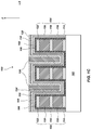
- FIGS. 1A through 1C are simplified cross-sectional views illustrating a method of forming a memory structure of a semiconductor device, in accordance with embodiments of the disclosure.
- FIG. 2 is a schematic block diagram illustrating an electronic system in accordance with embodiments of the disclosure.
- a memory structure includes memory cells on or over one or more conductive line structures, a first dielectric liner material (e.g., a first dielectric nitride material) on or over surfaces of the memory cells, a high-k dielectric material on or over surfaces of the first dielectric liner material, a second dielectric liner material (e.g., a second dielectric nitride material) on or over surfaces of the high-k dielectric material, and an additional dielectric material on or over surfaces of the second dielectric liner material.
- a first dielectric liner material e.g., a first dielectric nitride material
- a high-k dielectric material on or over surfaces of the first dielectric liner material
- a second dielectric liner material e.g., a second dielectric nitride material
- the second dielectric liner material may enhance the protection of the memory cells relative to the first dielectric liner material and the high-k dielectric material alone, and may prevent adverse interactions between the high-k dielectric material and one or more other materials (e.g., one or more precursor materials) during the formation of the additional dielectric material to ensure that the high-k dielectric material and the additional dielectric material exhibit desirable and predetermined properties.
- an oxide material e.g., a dielectric oxide material
- the oxide material may enhance adhesion between the second dielectric liner material and the additional dielectric material.
- the term “substrate” means and includes a base material or construction upon which additional materials are formed.
- the substrate may be a semiconductor substrate, a base semiconductor layer on a supporting structure, a metal electrode or a semiconductor substrate having one or more layers, structures or regions formed thereon.
- the substrate may be a conventional silicon substrate or other bulk substrate comprising a layer of semiconductive material.
- the term “bulk substrate” means and includes not only silicon wafers, but also silicon-on-insulator (SOI) substrates, such as silicon-on-sapphire (SOS) substrates and silicon-on-glass (SOG) substrates, epitaxial layers of silicon on a base semiconductor foundation, and other semiconductor or optoelectronic materials, such as silicon-germanium, germanium, gallium arsenide, gallium nitride, and indium phosphide.
- SOI silicon-on-insulator
- SOS silicon-on-sapphire
- SOOG silicon-on-glass
- epitaxial layers of silicon on a base semiconductor foundation and other semiconductor or optoelectronic materials, such as silicon-germanium, germanium, gallium arsenide, gallium nitride, and indium phosphide.
- the substrate may be doped or may be undoped.
- the term “configured” refers to a size, shape, material composition, and arrangement of one or more of at least one structure and at least one apparatus facilitating operation of one or more of the structure and the apparatus in a pre-determined way.
- spatially relative terms such as “beneath,” “below,” “lower,” “bottom,” “above,” “upper,” “top,” “front,” “rear,” “left,” “right,” and the like, may be used for ease of description to describe one element's or feature's relationship to another element(s) or feature(s) as illustrated in the figures.
- the spatially relative terms are intended to encompass different orientations of the materials in addition to the orientation depicted in the figures. For example, if materials in the figures are inverted, elements described as “below” or “beneath” or “under” or “on bottom of” other elements or features would then be oriented “above” or “on top of” the other elements or features.
- the term “below” can encompass both an orientation of above and below, depending on the context in which the term is used, which will be evident to one of ordinary skill in the art.
- the materials may be otherwise oriented (e.g., rotated 90 degrees, inverted, flipped, etc.) and the spatially relative descriptors used herein interpreted accordingly.
- the term “substantially” in reference to a given parameter, property, or condition means and includes to a degree that one of ordinary skill in the art would understand that the given parameter, property, or condition is met with a degree of variance, such as within acceptable manufacturing tolerances.
- the parameter, property, or condition may be at least 90.0% met, at least 95.0% met, at least 99.0% met, or even at least 99.9% met.
- the term “about” in reference to a given parameter is inclusive of the stated value and has the meaning dictated by the context (e.g., it includes the degree of error associated with measurement of the given parameter).
- FIGS. 1A through 1C are simplified perspective views illustrating embodiments of a method of forming a memory structure, such as a 3D cross-point memory structure of a semiconductor device (e.g., a memory device, such as a RRAM device, a conductive bridge RAM device, an MRAM device, a PCM memory device, a PCRAM device, an STTRAM device, an oxygen vacancy-based memory device, and/or a programmable conductor memory device).
- a memory device such as a RRAM device, a conductive bridge RAM device, an MRAM device, a PCM memory device, a PCRAM device, an STTRAM device, an oxygen vacancy-based memory device, and/or a programmable conductor memory device.
- a memory structure 100 may be formed to include at least one conductive line structure 102 , memory cells 104 , a first dielectric liner material 106 , a high-k dielectric material 108 , a second dielectric liner material 110 , and, optionally, an oxide material 124 .
- the memory cells 104 may be located on or over the at least one conductive line structure 102 , the first dielectric liner material 106 may be located on or over the memory cells 104 , the high-k dielectric material 108 may be located on or over the first dielectric liner material 106 , the second dielectric liner material 110 may be located on or over the high-k dielectric material 108 , and the oxide material 124 (if present) may be located on or over the second dielectric liner material 110 .
- the conductive line structure 102 may be formed of and include at least one conductive material, such as a metal, a metal alloy, a conductive metal oxide, a conductive metal nitride, a conductive metal silicide, a conductively doped semiconductor material, or combinations thereof.
- the conductive line structure 102 may be formed of and include one or more of tungsten (W), tungsten nitride (WN), nickel (Ni), tantalum (Ta), tantalum nitride (TaN), tantalum silicide (TaSi), platinum (Pt), copper (Cu), silver (Ag), gold (Au), aluminum (Al), molybdenum (Mo), titanium (Ti), titanium nitride (TiN), titanium silicide (TiSi), titanium silicon nitride (TiSiN), titanium aluminum nitride (TiAlN), molybdenum nitride (MoN), iridium (Ir), iridium oxide (IrO x ), ruthenium (Ru), ruthenium oxide (RuO x ), and conductively doped silicon.
- the conductive line structure 102 is formed of and includes W.
- the conductive line structure 102 is formed of and includes W.
- the conductive line structure 102 may be formed using conventional processes (e.g., conventional deposition processes, conventional material removal processes) and conventional processing equipment, which are not described in detail herein.
- a conductive material may be formed (e.g., through at least one of in situ growth, spin-on coating, blanket coating, chemical vapor deposition (CVD), plasma enhanced chemical vapor deposition (PECVD), atomic layer deposition (ALD), and physical vapor deposition (PVD)) and patterned (e.g., through at least one material removal process, such as at least one of a wet etching process and a dry etching process) to form the conductive line structure 102 .
- CVD chemical vapor deposition
- PECVD plasma enhanced chemical vapor deposition
- ALD atomic layer deposition
- PVD physical vapor deposition
- Each of the memory cells 104 may individually include a first electrode structure 114 on or over the conductive line structure 102 , a select device structure 116 on or over the first electrode structure 114 , an optional second electrode structure 118 on or over the select device structure 116 , a storage element structure 120 on or over the select device structure 116 (e.g., on or over the optional second electrode structure 118 ), and a third electrode structure 122 on or over the storage element structure 120 .
- the relative positions of the select device structure 116 and the storage element structure 120 may be switched.
- the storage element structure 120 may be located on or over the first electrode structure 114 , and the select device structure 116 may be located on or over the storage element structure 120 (e.g., on or over the optional second electrode structure 118 ).
- the select device structure 116 and the storage element structure 120 may comprise a single (e.g., only one) structure (e.g., a single resistance variable structure) able to perform the functions of the both the select device structure 116 and the storage element structure 120 (as described in further detail below).
- the first electrode structure 114 , the second electrode structure 118 (if present), and the third electrode structure 122 may serve as electrode contacts, and may each individually be formed of and include a conductive material, such as one or more of W, WN, Ni, Ta, TaN, TaSi, Pt, Cu, Ag, Au, Al, Mo, Ti, TiN, TiSi, TiSiN, TiAlN, MoN, Ir, IrO x , Ru, RuO x , conductively doped silicon, and a carbon material.
- a conductive material such as one or more of W, WN, Ni, Ta, TaN, TaSi, Pt, Cu, Ag, Au, Al, Mo, Ti, TiN, TiSi, TiSiN, TiAlN, MoN, Ir, IrO x , Ru, RuO x , conductively doped silicon, and a carbon material.
- the first electrode structure 114 , the second electrode structure 118 (if present), and the third electrode structure 122 may each be formed of and include substantially the same conductive material, or one or more of the first electrode structure 114 , the second electrode structure 118 (if present), and the third electrode structure 122 may be formed of and include a different conductive material than one or more other of the first electrode structure 114 , the second electrode structure 118 (if present), and the third electrode structure 122 .
- the first electrode structure 114 , the second electrode structure 118 (if present), and the third electrode structure 122 are each formed of and include a carbon material.
- carbon material means and includes material including carbon atoms.
- the carbon material may be substantially free of atoms other than carbon atoms, or may include carbon atoms and atoms of at least one additional element.
- one or more (e.g., each) of the first electrode structure 114 , the second electrode structure 118 (if present), and the third electrode structure 122 may be formed of and include a non-stoichiometric compound including carbon (C) atoms and nitrogen (N) atoms.
- non-stoichiometric compound means and includes a chemical compound with an elemental composition that cannot be represented by a ratio of well-defined natural numbers and is in violation of the law of definite and multiple proportions.
- One or more (e.g., each) of the first electrode structure 114 , the second electrode structure 118 (if present), and the third electrode structure 122 may, for example, include from about 80 atomic percent carbon to about 99.9 atomic percent carbon and from about 0.10 atomic percent nitrogen to about 20 atomic percent nitrogen.
- the select device structure 116 may be formed of and include at least one material configured and formulated relative to the material composition(s) of the other components (e.g., the conductive line structure 102 , the first electrode structure 114 , the second electrode structure 118 (if present)) of the memory structure 100 to form a switch for the storage element structure 120 .
- the select device structure 116 may be formed of and include one or more of at least one chalcogenide material, at least one semiconductor material, and at least one insulative material, which together with the other components of the memory structure 100 (e.g., the first electrode structure 114 and the second electrode structure 118 ) form a non-ohmic device (NOD) stack.
- NOD non-ohmic device
- the NOD stack may, for example, exhibit an ovonic threshold switch (OTS) configuration, a conductor-semiconductor-conductor (CSC) switch configuration, a metal-insulator-metal (MIM) switch configuration, a metal-semiconductor-metal (MSM) switch configuration, a metal-insulator-insulator-metal (MIIM) switch configuration, a metal-semiconductor-semiconductor-metal (MSSM) switch configuration, a metal-insulator-semiconductor-metal (MISM) switch configuration, a metal-semiconductor-insulator-metal (MSIM) switch configuration, a metal-insulator-semiconductor-insulator-metal (MISIM) switch configuration, a metal-insulator-semiconductor-insulator-metal (MISIM) switch configuration, a metal-semiconductor-insulator-semiconductor-metal (MSISM) switch
- the select device structure 116 is formed of and includes a chalcogenide compound.
- chalcogenide compound refers to a binary or multinary compound that includes at least one chalcogen atom and a more electropositive element or radical.
- chalcogen refers to an element of Group VI of the Periodic Table, such as oxygen (O), sulfur (S), selenium (Se), or tellurium (Te).
- the electropositive element may include, but is not limited to, nitrogen (N), silicon (Si), nickel (Ni), gallium (Ga), germanium (Ge), arsenic (As), silver (Ag), indium (In), tin (Sn), antimony (Sb), gold (Au), lead (Pb), bismuth (Bi), or combinations thereof.
- the chalcogenide compound may be a binary, ternary, or quaternary alloy.
- Non-limiting examples of suitable chalcogenide compounds for the select device structure 116 include As and Te compounds, such as As 2 Te 3 ; As and Se compounds, such as As 2 Se 3 ; As, Te, and Ge compounds, such as As 30 Te 45 Ge 25 ; As, Se, and Ge compounds, such as As 28 Se 42 Ge 30 ; As, S, Se, and Ge compounds, such as As 30 S 12 Se 33 Ge 25 ; and As, Te, Ge, Si, In compounds, such as As 37 Te 39 Ge 9 Si 14 In.
- the storage element structure 120 which may also be characterized as a programmable structure, may be formed of and include at least one resistance variable material.
- resistance variable material means and includes a material formulated to be switched from one resistance state to another resistance state upon application of at least one physical signal (e.g., at least one of heat, voltage, current, or other physical phenomena) thereto.
- Embodiments of the disclosure are not limited to a particular resistance variable material.
- the storage element structure 120 may, for example, be formed of and include a resistance variable material configured and formulated for one or more of RRAM, conductive bridge RAM, MRAM, PCM memory, PCRAM, STTRAM, oxygen vacancy-based memory, and programmable conductor memory.
- Suitable resistance variable materials include, but are not limited to, active switching materials (e.g., solid state electrolyte materials, such as transition metal oxide (TMO) materials, chalcogenide materials, dielectric metal oxide materials, mixed valence oxides including two or more metals and/or metalloids), metal ion source materials, oxygen-gettering materials, phase change materials, binary metal oxide materials, colossal magnetoresistive materials, and polymer-based resistance variable materials.
- active switching materials e.g., solid state electrolyte materials, such as transition metal oxide (TMO) materials, chalcogenide materials, dielectric metal oxide materials, mixed valence oxides including two or more metals and/or metalloids
- metal ion source materials e.g., oxygen-gettering materials, phase change materials, binary metal oxide materials, colossal magnetoresistive materials, and polymer-based resistance variable materials.
- the storage element structure 120 is formed of and includes a chalcogenide compound.
- the chalcogen may comprise one or more of O, S, Se, and Te.
- the electropositive element may include, but is not limited to, N, Si, Ni, Ga, Ge, As, Ag, In, Cd, Zn, Sn, Sb, Au, Pb, Bi, or combinations thereof.
- the chalcogenide compound may be a binary, ternary, or quaternary alloy.
- Non-limiting examples of suitable chalcogenide compounds for the storage element structure 120 include Sb and Te compounds, such as Sb 2 Te 3 ; Ge and Te compounds, such as GeTe; In and Se compounds, such as In 2 Se 3 ; Sn and Te compounds, such as SnTe; Bi and Te compounds, such as Bi 2 Te 3 ; Sb and Te compounds, such as SbTe, or Sb 2 Te 3 ; Sn and Se compounds, such as SnSe; Ge and Se compounds, such as GeSe; Ga, Se, and Te compounds, such as GaSeTe; Ge, Sb, and Te compounds, such as Ge 2 Sb 2 Te 5 ; Sn, Sb, and Te compounds, such as SnSb 2 Te 4 ; Au, Ge, Sn, and Te compounds, such as Au 25 Ge 4 Sn 11 Te 60 ; Au, In, Sb, and Te compounds, such as AuInSbTe; Ag and Se compounds, such as Ag 2 Se; In and Te compounds, such as InTe; and In
- the select device structure 116 and the storage element structure 120 may be formed of and include substantially the same material (e.g., substantially the same chalcogenide compound), or may be formed of and include different materials (e.g., different chalcogenide compounds). In some embodiments, the select device structure 116 and the storage element structure 120 are formed of and include different chalcogenide compounds than one another. In further embodiments, the select device structure 116 and the storage element structure 120 are formed of and include substantially the same chalcogenide compounds as one another.
- the select device structure 116 and the storage element structure 120 may comprise a single (e.g., only one) structure (e.g., a single self-selecting storage element structure) formed of and including a single material (e.g., a single chalcogenide compound), or may comprise a single (e.g., only one) structure formed of and including multiple (e.g., more than one) materials (e.g., multiple chalcogenide compounds).
- the memory structure 100 may include rows of the memory cells 104 extending in a first lateral direction (e.g., an X-direction) and columns of the memory cells 104 extending in a second lateral direction (e.g., a Y-direction) substantially perpendicular to the first lateral direction.
- the memory cells 104 within each row may be substantially aligned with one another, and the memory cells 104 within each column may also be substantially aligned with one another.
- adjacent (i.e., neighboring) memory cells 104 most proximate one another in the first lateral direction may be substantially aligned with one another in the second lateral direction (e.g., the Y-direction), and other adjacent memory cells 104 most proximate one another in the second lateral direction (e.g., the Y-direction) may be substantially aligned with one another in the first lateral direction (e.g., the X-direction).
- At least some adjacent memory cells 104 most proximate one another in the first lateral direction may be unaligned with (e.g., offset from) one another in the second lateral direction, and/or at least some adjacent memory cells 104 most proximate one another in the second lateral direction may be unaligned with (e.g., offset from) one another in the first lateral direction.
- the memory cells 104 may each individually exhibit any desired dimensions (e.g., length, width, diameter, height) and any desired shape. Each of the memory cells 104 may individually exhibit an aspect ratio (e.g., ratio of height to width or diameter) within a range of from about 1:1 to about 100:1, such as from about 5:1 to about 50:1, from about 10:1 to about 30:1; or from about 15:1 to about 25:1. In addition, in some embodiments, the memory cells 104 each individually exhibit a cylindrical column shape including a substantially circular lateral cross-sectional geometry.
- one or more of the memory cells 104 may exhibit a different shape, such as a rectangular column shape, a tube shape, a fin shape, a pillar shape, a stud shape, dome shape, a cone shape, a frusto cone shape, a pyramid shape, a frusto pyramid shape, or an irregular shape.
- Each of the memory cells 104 may exhibit substantially the same dimensions and substantially the same shape as each other of the memory cells 104 , or one or more of the memory cells 104 may exhibit at least one different dimension and/or a different shape than one or more other of the memory cells 104 .
- each of the memory cells 104 exhibits substantially the same dimensions and substantially the same shape as each other of the memory cells 104 .
- the memory cells 104 may exhibit any desired spacing relative to one another.
- Adjacent memory cells 104 within each row of the memory cells 104 may be substantially uniformly (e.g., substantially regularly) spaced apart from one another by a first distance
- adjacent memory cells 104 within each column of the memory cells 104 may be substantially uniformly (e.g., substantially regularly) spaced apart from one another by a second distance.
- the first distance may be substantially the same as the second distance, or the first distance may be different than the second distance.
- a pitch between centers of adjacent memory cells 104 within each of the rows may be substantially constant (e.g., non-variable)
- a pitch between centers of adjacent memory cells 104 within each of the columns may also be substantially constant (e.g., non-variable).
- At least some adjacent memory cells 104 within at least one row of the memory cells 104 are spaced apart from one another by a different distance than at least some other adjacent memory cells 104 within the row, and/or at least some adjacent memory cells 104 within at least one column of the memory cells 104 are spaced apart from one another by a different distance than at least some other adjacent memory cells 104 within the column. Accordingly, a pitch between centers of at least some adjacent memory cells 104 within at least one row may be different than a pitch between centers of at least some other adjacent memory cells 104 within the row, and/or a pitch between centers of at least some adjacent memory cells 104 within at least one column may be different than a pitch between centers of at least some other adjacent memory cells 104 within the column.
- the memory cells 104 including the various components thereof (e.g., the first electrode structure 114 , the select device structure 116 , the second electrode structure 118 (if any), the storage element structure 120 , the third electrode structure 122 ) may be formed using conventional processes (e.g., conventional deposition processes, conventional photolithography processes, conventional material removal processes) and conventional processing equipment, which are not described in detail herein.
- conventional processes e.g., conventional deposition processes, conventional photolithography processes, conventional material removal processes
- materials of the different components of the memory cells 104 may be formed (e.g., through one or more of in situ growth, spin-on coating, blanket coating, CVD, PECVD, ALD, and PVD) and patterned (e.g., through at least one material removal process, such as at least one of a wet etching process and a dry etching process) to form the memory cells 104 .
- the first dielectric liner material 106 may at least partially (e.g., substantially, completely) cover (e.g., surround, envelop) the memory cells 104 .
- the first dielectric liner material 106 adheres directly to the components (e.g., the first electrode structure 114 , the select device structure 116 , the second electrode structure 118 (if any), the storage element structure 120 , the third electrode structure 122 ) of the memory cells 104 , and may protect the memory cells 104 from damage (e.g., heat damage, chemical damage) that may otherwise occur to memory cells 104 during the formation of additional materials (e.g., the high-k dielectric material 108 ) over the memory cells 104 .
- damage e.g., heat damage, chemical damage
- the first dielectric liner material 106 may be configured (e.g., formulated, sized, shaped, positioned) to protect the memory cells 104 from a strong oxidizing environment that may be employed to form the high-k dielectric material 108 , as described in further detail below.
- the first dielectric liner material 106 may be conformally formed over the memory cells 104 .
- the first dielectric liner material 106 may comprise a dielectric material compatible with the materials of the memory cells 104 and the high-k dielectric material 108 .
- the term “compatible” means and includes that a material that does not react with, break down, or absorb another material in an unintended way, and that also does not impair the chemical and/or mechanical properties of the another material in an unintended way.
- the first dielectric liner material 106 may be formed of and include a dielectric nitride material, such as silicon nitride (SiN).
- the term “silicon nitride” means and includes a chemical compound including silicon atoms and nitrogen atoms, and includes stoichiometric and non-stoichiometric compounds of silicon and nitrogen, as well as a gradient of nitrogen atoms in the silicon.
- the first dielectric liner material 106 may be formed of and include a different dielectric material, such as one or more of silicon oxynitride (SiON), silicon carbonitride (SiCN), and silicon carboxynitride (SiOCN).
- silicon oxynitride means and includes a chemical compound including silicon atoms, nitrogen atoms, and oxygen atoms, and includes stoichiometric and non-stoichiometric compounds of silicon, nitrogen, and oxygen, as well as a gradient of nitrogen and oxygen atoms in the silicon.
- silicon carbonitride means and includes a chemical compound including silicon atoms, carbon atoms, and nitrogen atoms, and includes stoichiometric and non-stoichiometric compounds of silicon, carbon, and nitrogen, as well as a gradient of nitrogen and carbon atoms in the silicon.
- silicon carboxynitride means and includes a chemical compound including silicon atoms, carbon atoms, nitrogen atoms, and oxygen atoms, and includes stoichiometric and non-stoichiometric compounds of silicon, carbon, nitrogen, and oxygen, as well as a gradient of nitrogen, carbon, and oxygen atoms in the silicon.
- the first dielectric liner material 106 may be formed at any thickness sufficient to protect the memory cells 104 from damage during processing following the formation of the first dielectric liner material 106 , and facilitating desired dimensions and spacing of components of the memory structure 100 .
- an overall thickness of the first dielectric liner material 106 may be selected at least partially based on overall thicknesses of the high-k dielectric material 108 and the second dielectric liner material 110 to provide desired separation between adjacent memory cells 104 of the memory structure 100 .
- a thickness of the first dielectric liner material 106 may, for example, be less than or equal to about 100 Angstroms ( ⁇ ), such as within a range of from about 10 ⁇ to about 100 ⁇ , from about 25 ⁇ to about 100 ⁇ , from about 50 ⁇ to about 100 ⁇ , or from about 60 ⁇ to about 80 ⁇ . In some embodiments, a maximum thickness of the first dielectric liner material 106 is equal to about 66 ⁇ . In additional embodiments, a maximum thickness of the first dielectric liner material 106 is equal to about 100 ⁇ .
- the thickness of the first dielectric liner material 106 may be substantially uniform (e.g., non-variable, constant), or may be at least partially non-uniform (e.g., variable, non-constant).
- portions of the first dielectric liner material 106 overlying upper surfaces and side surfaces of the memory cells 104 may exhibit substantially the same thicknesses, or portions of the first dielectric liner material 106 overlying upper surfaces of the memory cells 104 may exhibit one or more different thicknesses (e.g., a larger thickness, a smaller thickness) than portions of the first dielectric liner material 106 overlying one or more side surfaces (e.g., side surfaces of one or more of the first electrode structure 114 , the select device structure 116 , the second electrode structure 118 (if any), the storage element structure 120 , and the third electrode structure 122 ) of the memory cells 104 .
- a different thicknesses e.g., a larger thickness, a smaller thickness
- side surfaces e.g., side surfaces of one or more of the first electrode structure 114 , the select device structure 116 , the second electrode structure 118 (if any), the storage element structure 120 , and the third electrode structure 122
- the first dielectric liner material 106 may be formed using conventional processes (e.g., conventional deposition processes, such as one or more of a CVD process, an ALD process, and a PVD process) and conventional processing equipment, which are not described in detail herein.
- the first dielectric liner material 106 may be formed by a low temperature (e.g., less than or equal to about 250° C.) CVD process, such as a capacitively coupled PECVD process, an inductively coupled plasma chemical vapor deposition (ICPCVD) process, a pulsed CVD process, or a remote plasma CVD process.
- a low temperature e.g., less than or equal to about 250° C.
- CVD process such as a capacitively coupled PECVD process, an inductively coupled plasma chemical vapor deposition (ICPCVD) process, a pulsed CVD process, or a remote plasma CVD process.
- the low temperature process for forming the first dielectric liner material 106 may be conducted with or without pulsing of the process power source.
- the first dielectric liner material 106 comprises SiN
- the first dielectric liner material 106 is formed by a pulsed PECVD process conducted at a temperature of less than about 250° C.
- the pulsed PECVD process may utilize conventional silicon reactant gases that do not contain carbon and conventional nitrogen reactant gases.
- the SiN may be formed using silane (SiH 4 ) and ammonia (NH 3 ) or silane and nitrogen gas (N 2 ) as the reactant gases.
- the pulsed PECVD process may also be free of chlorinated reagents or plasma treatments to mitigate damage (e.g., heat damage, chemical damage) to other components (e.g., the memory cells 104 , the conductive line structure 102 ) of the memory structure 100 .
- damage e.g., heat damage, chemical damage
- the high-k dielectric material 108 overlying the first dielectric liner material 106 may comprise a material having a dielectric constant greater than that of silicon dioxide (SiO 2 ).
- the term “dielectric constant” refers to the property of a particular bulk material, rather than the effective dielectric constant of a material as it is practically employed, which may be affected by material thickness or other factors.
- the high-k dielectric material 108 may reduce current leakage from and enhance the electrical performance of the memory cells 104 , and may be compatible with the materials of the first dielectric liner material 106 and the second dielectric liner material 110 .
- the high-k dielectric material 108 may be formed of and include one or more of hafnium oxide (HfO 2 ), nitrided hafnium oxide (HfON), hafnium silicate oxide, aluminum-doped hafnium oxide (HfAlO), aluminum oxide (Al 2 O 3 ), aluminum silicate oxide, zirconium oxide (ZrO 2 ), tantalum pentoxide (Ta 2 O 5 ), lanthanum oxide (La 2 O 3 ), titanium oxide (TiO 2 ), and yttrium oxide (Y 2 O 3 ).
- the high-k dielectric material 108 is formed of and includes Al 2 O 3 .
- the high-k dielectric material 108 may have any thickness able to provide the memory cells 104 with low current leakage and enhanced electrical performance, and facilitating desired dimensions and spacing of components of the memory structure 100 .
- An overall thickness of the high-k dielectric material 108 may be selected at least partially based on overall thicknesses of the first dielectric liner material 106 and the second dielectric liner material 110 to provide desired separation between adjacent memory cells 104 of the memory structure 100 .
- a thickness of the high-k dielectric material 108 may, for example, be less than or equal to about 25 ⁇ , such as within a range of from about 10 ⁇ to about 25 ⁇ , from about 15 ⁇ to about 25 ⁇ , from about 20 ⁇ to about 25 ⁇ .
- a maximum thickness of the first dielectric liner material 106 is equal to about 25 ⁇ . In additional embodiments, a maximum thickness of the high-k dielectric material 108 is equal to about 25 ⁇ .
- the thickness of the high-k dielectric material 108 may be substantially uniform (e.g., non-variable, constant), or may be at least partially non-uniform (e.g., variable, non-constant).
- portions of the high-k dielectric material 108 overlying upper surfaces and side surfaces of the memory cells 104 may exhibit substantially the same thickness, or portions of the first dielectric liner material 106 overlying one or more upper surfaces of the memory cells 104 may exhibit one or more different thicknesses (e.g., a larger thickness, a smaller thickness) than portions of the first dielectric liner material 106 overlying one or more side surfaces (e.g., side surfaces of one or more of the first electrode structure 114 , the select device structure 116 , the second electrode structure 118 (if any), the storage element structure 120 , and the third electrode structure 122 ) of the memory cells 104 .
- a larger thickness, a smaller thickness portions of the first dielectric liner material 106 overlying one or more side surfaces of the first electrode structure 114 , the select device structure 116 , the second electrode structure 118 (if any), the storage element structure 120 , and the third electrode structure 122
- the high-k dielectric material 108 may be formed using conventional processes (e.g., conventional deposition processes, such as one or more of a CVD process, a PECVD process, an ALD process, and a PVD process) and conventional processing equipment, which are not described in detail herein.
- conventional deposition processes such as one or more of a CVD process, a PECVD process, an ALD process, and a PVD process
- conventional processing equipment which are not described in detail herein.
- the high-k dielectric material 108 is formed of and includes Al 2 O 3
- the Al 2 O 3 may be formed by a low temperature ALD process by pulsing aluminum precursors and oxygen containing precursors sequentially.
- the second dielectric liner material 110 is formed on or over the high-k dielectric material 108 .
- the second dielectric liner material 110 may adhere directly to the high-k dielectric material 108 , and may facilitate the subsequent formation of one or more additional dielectric materials over the high-k dielectric material 108 without the formation of undesirable defects in the additional dielectric materials and/or the high-k dielectric material 108 , as described in further detail below.
- the second dielectric liner material 110 may be configured (e.g., formulated, sized, shaped, positioned) to circumvent negative effects on (e.g., impediments to) the polymerization of precursors employed to form the additional dielectric materials that may otherwise result from interactions (e.g., reactions) between the high-k dielectric material 108 and the precursors.
- the second dielectric liner material 110 may comprise a dielectric material compatible with the material compositions of the high-k dielectric material 108 and one or more materials (e.g., additional dielectric materials) to subsequently be formed on or over the second dielectric liner material 110 .
- the second dielectric liner material 110 may be formed of and include a dielectric nitride material, such as SiN.
- the first dielectric liner material 106 may be formed of and include a different dielectric material, such as one or more of SiON, SiCN, and SiOCN.
- the material composition of the second dielectric liner material 110 may be substantially the same as or may be different than the material composition of the first dielectric liner material 106 . In some embodiments, the material composition of the second dielectric liner material 110 is substantially the same as the material composition of the first dielectric liner material 106 . As a non-limiting example, the first dielectric liner material 106 and the second dielectric liner material 110 may be each formed of and include substantially the same formulation of SiN (e.g., substantially the same chemical compound including silicon atoms and nitrogen atoms, such as substantially the same stoichiometric compound of silicon and nitrogen, or substantially the same non-stoichiometric compound of silicon and nitrogen).
- SiN substantially the same chemical compound including silicon atoms and nitrogen atoms, such as substantially the same stoichiometric compound of silicon and nitrogen, or substantially the same non-stoichiometric compound of silicon and nitrogen.
- the first dielectric liner material 106 and the second dielectric liner material 110 may be each formed of and include substantially the same formulation of one or more of SiON, SiCN, and SiOCN.
- the material composition of the second dielectric liner material 110 is different than the material composition of the first dielectric liner material 106 .
- the first dielectric liner material 106 may be formed of and include one or more of SiN, SiON, SiCN, and SiOCN
- the second dielectric liner material 110 may be formed of and include one or more other of SiN, SiON, SiCN, and SiOCN.
- the first dielectric liner material 106 may be formed of and include a first formulation of SiN
- the second dielectric liner material 110 may be formed of and include a second, different formulation of SiN (e.g., a chemical compound including a different ratio of silicon atoms and nitrogen atoms).
- the first dielectric liner material 106 may be formed of and include a first formulation of one or more of SiON, SiCN, and SiOCN
- the second dielectric liner material 110 may be formed of and include a second, different formulation of one or more of SiON, SiCN, and SiOCN
- the first dielectric liner material 106 and the second dielectric liner material 110 may each be formed of SiON, but the second dielectric liner material 110 may comprise different amounts and/or distributions of silicon atoms, nitrogen atoms, and oxygen atoms than the first dielectric liner material 106
- the first dielectric liner material 106 and the second dielectric liner material 110 may each be formed of SiCN, but the second dielectric liner material 110 may comprise different amounts and/or distributions of silicon atoms, nitrogen atoms, and/or carbon atoms than the first dielectric liner material 106
- the first dielectric liner material 106 and the second dielectric liner material 110 may each be formed of
- the second dielectric liner material 110 may have any thickness facilitating the subsequent formation of one or more additional materials (e.g., additional dielectric materials) thereon or thereover, and facilitating desired dimensions and spacing of components of the memory structure 100 .
- an overall thickness of the second dielectric liner material 110 may be selected to substantially circumvent adverse interactions (e.g., adverse reactions, such as reactions impeding or preventing desired polymerization reactions) between the high-k dielectric material 108 thereunder and one or more materials (e.g., precursor materials) to be provided (e.g., deposited) thereover to form the additional materials.
- the overall thickness of the second dielectric liner material 110 may be selected at least partially based on overall thicknesses of the high-k dielectric material 108 and the first dielectric liner material 106 to provide desired separation between adjacent memory cells 104 of the memory structure 100 .
- a thickness of the second dielectric liner material 110 may, for example, be less than or equal to about 100 ⁇ , such as within a range of from about 10 ⁇ to about 100 ⁇ , from about 25 ⁇ to about 100 ⁇ , from about 50 ⁇ to about 100 ⁇ , or from about 60 ⁇ to about 80 ⁇ . In some embodiments, a maximum thickness of the second dielectric liner material 110 is equal to about 100 ⁇ .
- a maximum thickness of the second dielectric liner material 110 is equal to about 66 ⁇ .
- the thickness of the second dielectric liner material 110 may be substantially uniform (e.g., non-variable, constant), or may be at least partially non-uniform (e.g., variable, non-constant).
- portions of the second dielectric liner material 110 overlying upper surfaces and side surfaces of the memory cells 104 may exhibit substantially the same thicknesses, or portions of the second dielectric liner material 110 overlying upper surfaces of the memory cells 104 may exhibit one or more different thicknesses (e.g., a larger thickness, a smaller thickness) than portions of the second dielectric liner material 110 overlying one or more side surfaces of the memory cells 104 .
- the thickness (or thicknesses) of the second dielectric liner material 110 may be substantially the same as or may be different than (e.g., greater than, less than) the thickness (or thicknesses) of the first dielectric liner material 106 .
- the second dielectric liner material 110 and the first dielectric liner material 106 exhibit substantially the same thickness (or thicknesses) as one another.
- the second dielectric liner material 110 and the first dielectric liner material 106 may each exhibit a maximum thickness of about 83 ⁇ .
- the thickness (or thicknesses) of the second dielectric liner material 110 is less than the thickness (or thicknesses) of the first dielectric liner material 106 .
- the first dielectric liner material 106 may exhibit a maximum thickness of about 100 ⁇ and the second dielectric liner material 110 may exhibit a maximum thickness of about 66 ⁇ .
- the thickness (or thicknesses) of the second dielectric liner material 110 is greater than the thickness (or thicknesses) of the first dielectric liner material 106 .
- the first dielectric liner material 106 may exhibit a maximum thickness of about 66 ⁇ and the second dielectric liner material 110 may exhibit a maximum thickness of about 100 ⁇ .
- the second dielectric liner material 110 and the first dielectric liner material 106 may exhibit substantially the same thickness variability (or uniformity) as one another, or the second dielectric liner material 110 and the first dielectric liner material 106 may exhibit different thickness variabilities than one another.
- the thicknesses of the first dielectric liner material 106 and the second dielectric liner material 110 may each be substantially uniform (e.g., non-variable, constant).
- the first dielectric liner material 106 and the second dielectric liner material 110 may exhibit substantially the same variable (e.g., non-uniform, non-constant) thicknesses as one another.
- first dielectric liner material 106 and the second dielectric liner material 110 may each different variable (e.g., non-uniform, non-constant) thicknesses than one another.
- one of the first dielectric liner material 106 and the second dielectric liner material 110 may exhibit a substantially uniform thickness, and the other of the first dielectric liner material 106 and the second dielectric liner material 110 may exhibit a variable thickness.
- the second dielectric liner material 110 may be using conventional processes (e.g., conventional deposition processes, such as one or more of a CVD process, a PECVD process, an ALD process, and a PVD process) and conventional processing equipment, which are not described in detail herein.
- the second dielectric liner material 110 may be formed by a low temperature (e.g., less than or equal to about 250° C.), a CVD process, such as a capacitively coupled PECVD process, an ICPCVD process, a pulsed CVD process, or a remote plasma CVD process.
- the low temperature process for forming the second dielectric liner material 110 may be conducted with or without pulsing of the process power source.
- the second dielectric liner material 110 comprises SiN
- the second dielectric liner material 110 is formed by a pulsed PECVD process conducted at a temperature of less than about 250° C.
- the pulsed PECVD process may utilize conventional silicon reactant gases that do not contain carbon and conventional nitrogen reactant gases.
- the SiN may be formed using silane (SiH 4 ) and ammonia (NH 3 ) or silane and nitrogen gas (N 2 ) as the reactant gases.
- the pulsed PECVD process may also be free of chlorinated reagents or plasma treatments to mitigate damage (e.g., heat damage, chemical damage) to other components (e.g., the memory cells 104 , the first dielectric liner material 106 , the high-k dielectric material 108 , the conductive line structure 102 ) of the memory structure 100 .
- the processes employed to form the second dielectric liner material 110 may be substantially the same as or may be different than the processes employed to form the first dielectric liner material 106 .
- the oxide material 124 may be formed on or over the second dielectric liner material 110 . If present, the oxide material 124 may provide enhanced adhesion strength between the second dielectric liner material 110 and one or more additional materials (e.g., additional dielectric materials) to be formed thereover relative to forming the one or more additional dielectric materials directly on the second dielectric liner material 110 , thereby reducing a risk of delamination.
- additional materials e.g., additional dielectric materials
- the oxide material 124 may comprise an oxide material compatible with the material compositions of the second dielectric liner material 110 and one or more materials (e.g., additional dielectric materials) to subsequently be formed over the oxide material 124 .
- the oxide material 124 may be formed of and include a dielectric oxide material, such as a silicon oxide material (e.g., SiO 2 , phosphosilicate glass, borosilicate glass, borophosphosilicate glass, or combinations thereof).
- the oxide material 124 comprises SiO 2 .
- the oxide material 124 comprises one or more of phosphosilicate glass, borosilicate glass, and borophosphosilicate glass.
- the oxide material 124 is absent (e.g., omitted) from the memory structure 100 .
- the oxide material 124 may have any thickness facilitating the subsequent formation of one or more additional materials (e.g., additional dielectric materials) thereon or thereover, and facilitating desired dimensions and spacing of components of the memory structure 100 .
- an overall thickness of the oxide material 124 may be selected at least partially based on overall thicknesses of the first dielectric liner material 106 , the high-k dielectric material 108 , and the second dielectric liner material 110 to provide desired separation between adjacent memory cells 104 of the memory structure 100 .
- a thickness of the oxide material 124 may, for example, be less than or equal to about 10 ⁇ , such as less than or equal to about 5 ⁇ , or less than or equal to about 2 ⁇ .
- the oxide material 124 comprises a single (e.g., only one) atomic layer (e.g., a monolayer) of dielectric oxide material (e.g., silicon oxide material) on the second dielectric liner material 110 .
- the thickness of the oxide material 124 may be substantially uniform (e.g., non-variable, constant), or may be at least partially non-uniform (e.g., variable, non-constant). In some embodiments, the thickness of the oxide material 124 is substantially uniform.
- the oxide material 124 may be formed using conventional processes (e.g., conventional deposition processes, such as one or more of a CVD process, a PECVD process, an ALD process, and a PVD process) and conventional processing equipment, which are not described in detail herein.
- the oxide material 124 is formed using an ALD process.
- the SiO 2 may be formed by a low temperature ALD process by pulsing silicon precursors and oxygen containing precursors sequentially.
- At least one additional dielectric material 126 may be formed on or over the second dielectric liner material 110 (e.g., on the oxide material 124 , if present; on the second dielectric liner material 110 if the oxide material 124 is absent). As shown in FIG. 1B , the additional dielectric material 126 laterally intervenes between adjacent memory cells 104 of the memory structure 100 , and may substantially completely fill remaining spaces (e.g., spaces unoccupied by the first dielectric liner material 106 , the high-k dielectric material 108 , the second dielectric liner material 110 , and the oxide material 124 (if any)) between the adjacent memory cells 104 .
- the additional dielectric material 126 may electrically isolate adjacent memory cells 104 of the memory structure 100 from one another.
- the additional dielectric material 126 may also longitudinally overlie the memory cells 104 of the memory structure 100 .
- An upper surface of the additional dielectric material 126 may be substantially planar, and may be positioned longitudinally above upper surfaces of the memory cells 104 .
- the additional dielectric material 126 may comprise a dielectric material compatible with the material composition of the second dielectric liner material 110 (and the oxide material 124 , if present).
- the additional dielectric material 126 may be formed of and include a carbonated dielectric oxide material.
- the additional dielectric material 126 is a carbonated silicon oxide (SiOC).
- SiOC carbonated silicon oxide
- carbonated silicon oxide means and includes a chemical compound including silicon atoms, carbon atoms, and oxygen atoms, and includes stoichiometric and non-stoichiometric compounds of silicon, carbon, and oxygen, as well as a gradient of oxygen and carbon atoms in the silicon.
- the carbonated dielectric oxide material may include any suitable amount of carbon atoms.
- the carbonated dielectric oxide material may comprise from about five (5) atomic percent (atomic %) carbon to about sixty (60) atomic % carbon, such as from about ten (10) atomic % carbon to about fifty-five atomic % carbon, or from about fifteen (15) atomic % carbon to about fifty (50) atomic % carbon.
- the carbonated dielectric oxide material comprises about fifty (50) atomic % carbon.
- the carbonated dielectric oxide material comprises about fifteen (15) atomic % carbon.
- covering e.g., surrounding, encapsulating
- the high-k dielectric material 108 with the second dielectric liner material 110 prior to the formation of the additional dielectric material 126 over the high-k dielectric material 108 may prevent adverse interactions (e.g., adverse reactions) between the high-k dielectric material 108 and one or more of the additional dielectric material 126 and precursors to the additional dielectric material 126 that may otherwise impact desirable properties of the additional dielectric material 126 and/or the high-k dielectric material 108 .
- covering the high-k dielectric material 108 with the second dielectric liner material 110 may prevent changes (e.g., physical changes, chemical changes) to the additional dielectric material 126 resulting from interactions between the high-k dielectric material 108 and the additional dielectric material 126 that may undesirably soften the additional dielectric material 126 .
- Such a softened additional dielectric material 126 may be more susceptible to damage (e.g., gouging) and/or defects (e.g., embedded particles, such as embedded chemical-mechanical planarization slurry particles) during subsequent processing of the memory structure 100 .
- the additional dielectric material 126 may be formed using conventional processes (e.g., conventional deposition processes, such as one or more of spin-on coating, blanket coating, in situ growth, CVD, ALD, and PVD; conventional densification processes) and conventional processing equipment, which are not described in detail herein.
- the additional dielectric material 126 is formed over the second dielectric liner material 110 through a spin-on coating process.
- the memory structure 100 may be subjected to at least one material removal process to remove a portion of the additional dielectric material 126 .
- the memory structure 100 may be subjected to at least one chemical-mechanical planarization (CMP) process to reduce a height of the additional dielectric material 126 , and form a planar surface 128 for the memory structure 100 .
- CMP process may include polishing at least the additional dielectric material 126 using at least one CMP slurry and at least one polishing pad.
- the CMP slurry may, for example, include abrasive particles, at least one solvent (e.g., water), and at least one chemically reactive material formulated to remove the additional dielectric material 126 .
- Covering (e.g., surrounding, encapsulating) the high-k dielectric material 108 with the second dielectric liner material 110 may enhance CMP processing efficiency (e.g., may enhance one or more of material removal rates, material removal detectability, and CMP polishing pad longevity), may improve removal profile consistency (e.g., may enhance material removal uniformity across lateral dimensions of the memory structure 100 ), and may maintain the integrity of the high-k dielectric material 108 (e.g., may protect the high-k dielectric material 108 from adverse interactions with the solvent of the CMP slurry).
- the planar surface 128 of the memory structure 100 may be defined by upper surfaces of remaining portions of the additional dielectric material 126 , and upper surfaces of the second dielectric liner material 110 substantially coplanar with the upper surfaces of the remaining portions of the additional dielectric material 126 .
- the second dielectric liner material 110 may protect the high-k dielectric material 108 from removal during the material removal process (e.g. CMP process).
- the planar surface 128 of the memory structure 100 may only be defined by an upper surface of the additional dielectric material 126 .
- Upper surfaces of the second dielectric liner material 110 may, for example, be completely covered by remaining portions of the additional dielectric material 126 following the material removal process.
- the planar surface 128 of the memory structure 100 may be defined by upper surfaces of remaining portions of the additional dielectric material 126 , and upper surfaces of one or more components of the memory structure 100 other than the second dielectric liner material 110 .
- the planar surface 128 of the memory structure 100 may be defined by the upper surfaces of remaining portions of the additional dielectric material 126 and upper surfaces of the high-k dielectric material 108 , or may be defined by the upper surfaces of remaining portions of the additional dielectric material 126 and upper surfaces of the oxide material 124 .
- a method of forming a memory structure comprises forming a first dielectric liner material over memory cells.
- a high-k dielectric material is formed over the first dielectric liner material.
- a second dielectric liner material is formed over the high-k dielectric material.
- An additional dielectric material is formed over the second dielectric liner material.
- the memory structure 100 may be subjected to additional processing (e.g., additional material removal processes, additional material deposition processes).
- additional processing e.g., additional material removal processes, additional material deposition processes.
- the memory structure 100 may be subjected to at least one additional material removal process to at least partially expose (e.g., uncover) upper surfaces of the third electrode structures 122 of the memory cells 104 , and one or more materials (e.g., one or more conductive materials) may be formed on or over the exposed portions of the upper surfaces of the third electrode structures 122 .
- Side surfaces of the memory cells 104 may remain substantially covered (e.g., surrounded, encapsulated) by one or more (e.g., each) of the first dielectric liner material 106 , the high-k dielectric material 108 , the second dielectric liner material 110 , the oxide material 124 (if any), and the additional dielectric material 126 .
- side surfaces of the memory cells 104 may remain substantially covered by the first dielectric liner material 106
- side surfaces of the first dielectric liner material 106 may remain substantially covered by the high-k dielectric material 108
- side surfaces of the high-k dielectric material 108 may remain substantially covered by the second dielectric liner material 110
- side surfaces of the second dielectric liner material 110 may remain substantially covered by the additional dielectric material 126 .
- a semiconductor device comprises memory cells, a first dielectric liner material overlying the memory cells, a high-k dielectric material overlying the first dielectric liner material, a second dielectric liner material overlying the high-k dielectric material, and an additional dielectric material overlying the second dielectric liner material.
- the memory structure 100 may be used in a wide variety of semiconductor devices including, but not limited to memory devices (e.g., resistive memory devices, such as RRAM devices).
- Semiconductor devices that include the memory structure 100 in accordance with embodiments of the disclosure may be included in a variety of electronic systems.
- FIG. 2 is a block diagram of an electronic system 200 according to embodiments of disclosure.
- the electronic system 200 may comprise, for example, a computer or computer hardware component, a server or other networking hardware component, a cellular telephone, a digital camera, a personal digital assistant (PDA), portable media (e.g., music) player, etc.
- the electronic system 200 includes at least one semiconductor device 202 (e.g., at least one memory device).
- the electronic system 200 may further include at least one electronic signal processor device 204 (often referred to as a “microprocessor”).
- a microprocessor an electronic signal processor device 204
- One or more of the semiconductor device 202 and the electronic signal processor device 204 may include, for example, an embodiment of the memory structure 100 previously described with respect to FIGS. 1A-1C .
- the electronic system 200 may further include one or more input devices 206 for inputting information into the electronic system 200 by a user, such as, for example, a mouse or other pointing device, a keyboard, a touchpad, a button, or a control panel.
- the electronic system 200 may further include one or more output devices 208 for outputting information (e.g., visual or audio output) to a user such as, for example, a monitor, a display, a printer, an audio output jack, a speaker, etc.
- the input device 206 and the output device 208 may comprise a single touch screen device that can be used both to input information to the electronic system 200 and to output visual information to a user.
- the one or more input devices 206 and output devices 208 may communicate electrically with at least one of the semiconductor device 202 and the electronic signal processor device 204 .
- an electronic system comprises a memory device in communication with at least one of an electronic signal processor device, an input device, and an output device.
- the memory device includes a memory structure comprising memory cells, a first dielectric nitride material on side surfaces of the memory cells, a high-k dielectric material on side surfaces of the first dielectric nitride material, a second dielectric nitride material on side surfaces of the high-k dielectric material, and an additional dielectric material over side surfaces of the second dielectric nitride material.
Landscapes
- Engineering & Computer Science (AREA)
- Manufacturing & Machinery (AREA)
- Chemical & Material Sciences (AREA)
- Crystallography & Structural Chemistry (AREA)
- Semiconductor Memories (AREA)
Abstract
Description
Claims (19)
Priority Applications (1)
| Application Number | Priority Date | Filing Date | Title |
|---|---|---|---|
| US16/202,891 US10693063B2 (en) | 2017-08-31 | 2018-11-28 | Methods of forming a memory structure |
Applications Claiming Priority (2)
| Application Number | Priority Date | Filing Date | Title |
|---|---|---|---|
| US15/692,599 US10147875B1 (en) | 2017-08-31 | 2017-08-31 | Semiconductor devices and electronic systems having memory structures |
| US16/202,891 US10693063B2 (en) | 2017-08-31 | 2018-11-28 | Methods of forming a memory structure |
Related Parent Applications (1)
| Application Number | Title | Priority Date | Filing Date |
|---|---|---|---|
| US15/692,599 Division US10147875B1 (en) | 2017-08-31 | 2017-08-31 | Semiconductor devices and electronic systems having memory structures |
Publications (2)
| Publication Number | Publication Date |
|---|---|
| US20190165263A1 US20190165263A1 (en) | 2019-05-30 |
| US10693063B2 true US10693063B2 (en) | 2020-06-23 |
Family
ID=64451708
Family Applications (2)
| Application Number | Title | Priority Date | Filing Date |
|---|---|---|---|
| US15/692,599 Active US10147875B1 (en) | 2017-08-31 | 2017-08-31 | Semiconductor devices and electronic systems having memory structures |
| US16/202,891 Active US10693063B2 (en) | 2017-08-31 | 2018-11-28 | Methods of forming a memory structure |
Family Applications Before (1)
| Application Number | Title | Priority Date | Filing Date |
|---|---|---|---|
| US15/692,599 Active US10147875B1 (en) | 2017-08-31 | 2017-08-31 | Semiconductor devices and electronic systems having memory structures |
Country Status (2)
| Country | Link |
|---|---|
| US (2) | US10147875B1 (en) |
| CN (2) | CN118338679A (en) |
Cited By (1)
| Publication number | Priority date | Publication date | Assignee | Title |
|---|---|---|---|---|
| US12262641B2 (en) | 2021-02-05 | 2025-03-25 | Samsung Electronics Co., Ltd. | Magnetic memory device and method of fabricating the same |
Families Citing this family (20)
| Publication number | Priority date | Publication date | Assignee | Title |
|---|---|---|---|---|
| US10020363B2 (en) * | 2016-11-03 | 2018-07-10 | Sandisk Technologies Llc | Bulb-shaped memory stack structures for direct source contact in three-dimensional memory device |
| US10147875B1 (en) * | 2017-08-31 | 2018-12-04 | Micron Technology, Inc. | Semiconductor devices and electronic systems having memory structures |
| US11189662B2 (en) * | 2018-08-13 | 2021-11-30 | Micron Technology | Memory cell stack and via formation for a memory device |
| US10991425B2 (en) | 2018-08-13 | 2021-04-27 | Micron Technology, Inc. | Access line grain modulation in a memory device |
| US10777275B2 (en) * | 2018-09-26 | 2020-09-15 | Intel Corporation | Reset refresh techniques for self-selecting memory |
| KR102821718B1 (en) * | 2019-03-05 | 2025-06-18 | 에스케이하이닉스 주식회사 | Electronic device and method for fabricating the same |
| US11538988B2 (en) * | 2019-03-07 | 2022-12-27 | Intel Corporation | Memory device with multi-layer liner structure |
| US10770653B1 (en) | 2019-07-18 | 2020-09-08 | International Business Machines Corporation | Selective dielectric deposition to prevent gouging in MRAM |
| KR102763600B1 (en) | 2019-10-07 | 2025-02-10 | 삼성전자주식회사 | Variable resistance memory Device |
| US11444243B2 (en) * | 2019-10-28 | 2022-09-13 | Micron Technology, Inc. | Electronic devices comprising metal oxide materials and related methods and systems |
| US11373695B2 (en) | 2019-12-18 | 2022-06-28 | Micron Technology, Inc. | Memory accessing with auto-precharge |
| US11424118B2 (en) | 2020-01-23 | 2022-08-23 | Micron Technology, Inc. | Electronic devices comprising silicon carbide materials |
| US11393756B2 (en) | 2020-03-16 | 2022-07-19 | Micron Technology, Inc. | Methods of forming microelectronic devices, and related microelectronic devices, memory devices, and electronic systems |
| US11430950B2 (en) | 2020-03-27 | 2022-08-30 | Micron Technology, Inc. | Low resistance via contacts in a memory device |
| FR3112018A1 (en) * | 2020-06-30 | 2021-12-31 | Stmicroelectronics (Rousset) Sas | Phase change memory cell isolation |
| US11979171B2 (en) | 2020-10-13 | 2024-05-07 | Microchip Technology Incorporated | Reduced complexity encoders and related systems, methods, and devices |
| CN113611658A (en) * | 2020-12-30 | 2021-11-05 | 联芯集成电路制造(厦门)有限公司 | Semiconductor element |
| US11551926B2 (en) | 2021-01-22 | 2023-01-10 | Micron Technology, Inc. | Methods of forming a microelectronic device, and related systems and additional methods |
| CN116568043A (en) * | 2022-01-26 | 2023-08-08 | 联华电子股份有限公司 | Semiconductor memory element and manufacturing method thereof |
| US20240234482A9 (en) * | 2022-10-19 | 2024-07-11 | Micron Technology, Inc. | Microelectronic devices including capacitors, and related electronic systems and methods |
Citations (40)
| Publication number | Priority date | Publication date | Assignee | Title |
|---|---|---|---|---|
| US6753570B1 (en) * | 2002-08-20 | 2004-06-22 | Advanced Micro Devices, Inc. | Memory device and method of making |
| US6764966B1 (en) * | 2002-02-27 | 2004-07-20 | Advanced Micro Devices, Inc. | Spacers with a graded dielectric constant for semiconductor devices having a high-K dielectric |
| US20080265306A1 (en) * | 2005-12-15 | 2008-10-30 | Nxp B.V. | Non-Volatile Memory Device Having a Gap in the Tunnuel Insulating Layer and Method of Manufacturing the Same |
| US20090289306A1 (en) * | 2008-05-21 | 2009-11-26 | Kabushiki Kaisha Toshiba | Lateral oxidation with high-k dielectric liner |
| US7674698B2 (en) * | 2005-07-07 | 2010-03-09 | Micron Technology, Inc. | Metal-substituted transistor gates |
| US20100248465A1 (en) * | 2009-03-24 | 2010-09-30 | In-Sun Yi | Methods of fabricating silicon oxide layers using inorganic silicon precursors and methods of fabricating semiconductor devices including the same |
| US20110018047A1 (en) * | 2009-06-30 | 2011-01-27 | Kabushiki Kaisha Toshiba | Nonvolatile semiconductor memory device and method of manufacturing the same |
| US8053302B2 (en) | 2008-08-21 | 2011-11-08 | Samsung Electronics Co., Ltd. | Non-volatile memory device and method of manufacturing same |
| US20130092894A1 (en) * | 2011-10-17 | 2013-04-18 | Micron Technology, Inc. | Memory cells and memory cell arrays |
| US20130126812A1 (en) * | 2011-11-17 | 2013-05-23 | Micron Technology, Inc. | Memory Cells, Integrated Devices, and Methods of Forming Memory Cells |
| US20130313576A1 (en) * | 2011-02-02 | 2013-11-28 | Rohm Co., Ltd. | Semiconductor power device and method for producing same |
| US20140070304A1 (en) * | 2012-09-11 | 2014-03-13 | Kabushiki Kaisha Toshiba | Nonvolatile memory device and method for manufacturing same |
| US20150060992A1 (en) | 2013-09-02 | 2015-03-05 | Kim Taekyung | Semiconductor device, systems and methods of manufacture |
| US20150263018A1 (en) * | 2014-03-11 | 2015-09-17 | Kabushiki Kaisha Toshiba | Semiconductor device and method of manufacturing the same |
| US20150287916A1 (en) * | 2014-04-03 | 2015-10-08 | Micron Technology, Inc. | Semiconductor structures including multi-portion liners and related methods |
| US20150318038A1 (en) | 2014-04-30 | 2015-11-05 | Micron Technology, Inc. | Phase change memory stack with treated sidewalls |
| US9269718B1 (en) * | 2014-09-05 | 2016-02-23 | Kabushiki Kaisha Toshiba | Manufacturing method of semiconductor memory device |
| US9281471B2 (en) | 2014-04-30 | 2016-03-08 | Micron Technology, Inc. | Phase change memory stack with treated sidewalls |
| US20160071861A1 (en) | 2014-09-05 | 2016-03-10 | Sandisk Technologies Inc. | 3d semicircular vertical nand string with self aligned floating gate or charge trap cell memory cells and methods of fabricating and operating the same |
| US20160079434A1 (en) * | 2014-09-11 | 2016-03-17 | Kabushiki Kaisha Toshiba | Semiconductor device |
| US9305933B2 (en) | 2011-05-24 | 2016-04-05 | Samsung Electronics Co., Ltd. | Methods of forming semiconductor memory devices |
| US20160104719A1 (en) | 2014-10-14 | 2016-04-14 | Won-Seok Jung | Semiconductor Memory Devices and Methods of Fabricating the Same |
| US20160118391A1 (en) | 2014-10-22 | 2016-04-28 | SanDisk Technologies, Inc. | Deuterium anneal of semiconductor channels in a three-dimensional memory structure |
| US9397143B2 (en) | 2013-12-20 | 2016-07-19 | Intel Corporation | Liner for phase change memory (PCM) array and associated techniques and configurations |
| US9484358B2 (en) | 2010-06-30 | 2016-11-01 | Sandisk Technologies Llc | Ultrahigh density vertical NAND memory device and method of making thereof |
| US9484357B2 (en) | 2014-12-16 | 2016-11-01 | Sandisk Technologies Llc | Selective blocking dielectric formation in a three-dimensional memory structure |
| US20160358933A1 (en) | 2015-06-08 | 2016-12-08 | Sandisk Technologies Inc. | Method of making a three-dimensional memory device having a heterostructure quantum well channel |
| US9524984B1 (en) | 2015-08-24 | 2016-12-20 | SK Hynix Inc. | 3D semiconductor device with enhanced performance |
| US20170062456A1 (en) | 2015-08-31 | 2017-03-02 | Cypress Semiconductor Corporation | Vertical division of three-dimensional memory device |
| US20170117289A1 (en) | 2015-10-26 | 2017-04-27 | Sandisk Technologies Inc. | Methods and apparatus for three-dimensional nand non-volatile memory devices with side source line and mechanical support |
| US9666525B2 (en) | 2015-08-28 | 2017-05-30 | Samsung Electronics Co., Ltd. | Three-dimensional semiconductor memory device |
| US9748266B1 (en) | 2016-07-20 | 2017-08-29 | Sandisk Technologies Llc | Three-dimensional memory device with select transistor having charge trapping gate dielectric layer and methods of making and operating thereof |
| US9748267B2 (en) | 2014-06-27 | 2017-08-29 | Sandisk Technologies Llc | Three dimensional NAND device with channel contacting conductive source line and method of making thereof |
| US9876027B2 (en) | 2013-12-19 | 2018-01-23 | Sandisk Technologies Llc | Three dimensional NAND device with channel located on three sides of lower select gate and method of making thereof |
| US20180090313A1 (en) * | 2016-09-28 | 2018-03-29 | Samsung Electronics Co., Ltd. | Method for forming dielectric film and method for fabricating semiconductor device |
| US9985098B2 (en) | 2016-11-03 | 2018-05-29 | Sandisk Technologies Llc | Bulb-shaped memory stack structures for direct source contact in three-dimensional memory device |
| US9997535B2 (en) * | 2016-03-18 | 2018-06-12 | Toshiba Memory Corporation | Semiconductor memory device and method of manufacturing the same |
| US10147875B1 (en) * | 2017-08-31 | 2018-12-04 | Micron Technology, Inc. | Semiconductor devices and electronic systems having memory structures |
| US20190198630A1 (en) * | 2017-12-21 | 2019-06-27 | Macronix International Co., Ltd. | Managing Gate Coupling For Memory Devices |
| US10396125B2 (en) * | 2014-11-07 | 2019-08-27 | Micron Technology, Inc. | Cross-point memory and methods for fabrication of same |
Family Cites Families (1)
| Publication number | Priority date | Publication date | Assignee | Title |
|---|---|---|---|---|
| US9343317B2 (en) * | 2013-07-01 | 2016-05-17 | Micron Technology, Inc. | Methods of forming silicon-containing dielectric materials and semiconductor device structures |
-
2017
- 2017-08-31 US US15/692,599 patent/US10147875B1/en active Active
-
2018
- 2018-08-31 CN CN202410434472.1A patent/CN118338679A/en active Pending
- 2018-08-31 CN CN201811009405.6A patent/CN109427842A/en active Pending
- 2018-11-28 US US16/202,891 patent/US10693063B2/en active Active
Patent Citations (40)
| Publication number | Priority date | Publication date | Assignee | Title |
|---|---|---|---|---|
| US6764966B1 (en) * | 2002-02-27 | 2004-07-20 | Advanced Micro Devices, Inc. | Spacers with a graded dielectric constant for semiconductor devices having a high-K dielectric |
| US6753570B1 (en) * | 2002-08-20 | 2004-06-22 | Advanced Micro Devices, Inc. | Memory device and method of making |
| US7674698B2 (en) * | 2005-07-07 | 2010-03-09 | Micron Technology, Inc. | Metal-substituted transistor gates |
| US20080265306A1 (en) * | 2005-12-15 | 2008-10-30 | Nxp B.V. | Non-Volatile Memory Device Having a Gap in the Tunnuel Insulating Layer and Method of Manufacturing the Same |
| US20090289306A1 (en) * | 2008-05-21 | 2009-11-26 | Kabushiki Kaisha Toshiba | Lateral oxidation with high-k dielectric liner |
| US8053302B2 (en) | 2008-08-21 | 2011-11-08 | Samsung Electronics Co., Ltd. | Non-volatile memory device and method of manufacturing same |
| US20100248465A1 (en) * | 2009-03-24 | 2010-09-30 | In-Sun Yi | Methods of fabricating silicon oxide layers using inorganic silicon precursors and methods of fabricating semiconductor devices including the same |
| US20110018047A1 (en) * | 2009-06-30 | 2011-01-27 | Kabushiki Kaisha Toshiba | Nonvolatile semiconductor memory device and method of manufacturing the same |
| US9484358B2 (en) | 2010-06-30 | 2016-11-01 | Sandisk Technologies Llc | Ultrahigh density vertical NAND memory device and method of making thereof |
| US20130313576A1 (en) * | 2011-02-02 | 2013-11-28 | Rohm Co., Ltd. | Semiconductor power device and method for producing same |
| US9305933B2 (en) | 2011-05-24 | 2016-04-05 | Samsung Electronics Co., Ltd. | Methods of forming semiconductor memory devices |
| US20130092894A1 (en) * | 2011-10-17 | 2013-04-18 | Micron Technology, Inc. | Memory cells and memory cell arrays |
| US20130126812A1 (en) * | 2011-11-17 | 2013-05-23 | Micron Technology, Inc. | Memory Cells, Integrated Devices, and Methods of Forming Memory Cells |
| US20140070304A1 (en) * | 2012-09-11 | 2014-03-13 | Kabushiki Kaisha Toshiba | Nonvolatile memory device and method for manufacturing same |
| US20150060992A1 (en) | 2013-09-02 | 2015-03-05 | Kim Taekyung | Semiconductor device, systems and methods of manufacture |
| US9876027B2 (en) | 2013-12-19 | 2018-01-23 | Sandisk Technologies Llc | Three dimensional NAND device with channel located on three sides of lower select gate and method of making thereof |
| US9397143B2 (en) | 2013-12-20 | 2016-07-19 | Intel Corporation | Liner for phase change memory (PCM) array and associated techniques and configurations |
| US20150263018A1 (en) * | 2014-03-11 | 2015-09-17 | Kabushiki Kaisha Toshiba | Semiconductor device and method of manufacturing the same |
| US20150287916A1 (en) * | 2014-04-03 | 2015-10-08 | Micron Technology, Inc. | Semiconductor structures including multi-portion liners and related methods |
| US20150318038A1 (en) | 2014-04-30 | 2015-11-05 | Micron Technology, Inc. | Phase change memory stack with treated sidewalls |
| US9281471B2 (en) | 2014-04-30 | 2016-03-08 | Micron Technology, Inc. | Phase change memory stack with treated sidewalls |
| US9748267B2 (en) | 2014-06-27 | 2017-08-29 | Sandisk Technologies Llc | Three dimensional NAND device with channel contacting conductive source line and method of making thereof |
| US20160071861A1 (en) | 2014-09-05 | 2016-03-10 | Sandisk Technologies Inc. | 3d semicircular vertical nand string with self aligned floating gate or charge trap cell memory cells and methods of fabricating and operating the same |
| US9269718B1 (en) * | 2014-09-05 | 2016-02-23 | Kabushiki Kaisha Toshiba | Manufacturing method of semiconductor memory device |
| US20160079434A1 (en) * | 2014-09-11 | 2016-03-17 | Kabushiki Kaisha Toshiba | Semiconductor device |
| US20160104719A1 (en) | 2014-10-14 | 2016-04-14 | Won-Seok Jung | Semiconductor Memory Devices and Methods of Fabricating the Same |
| US20160118391A1 (en) | 2014-10-22 | 2016-04-28 | SanDisk Technologies, Inc. | Deuterium anneal of semiconductor channels in a three-dimensional memory structure |
| US10396125B2 (en) * | 2014-11-07 | 2019-08-27 | Micron Technology, Inc. | Cross-point memory and methods for fabrication of same |
| US9484357B2 (en) | 2014-12-16 | 2016-11-01 | Sandisk Technologies Llc | Selective blocking dielectric formation in a three-dimensional memory structure |
| US20160358933A1 (en) | 2015-06-08 | 2016-12-08 | Sandisk Technologies Inc. | Method of making a three-dimensional memory device having a heterostructure quantum well channel |
| US9524984B1 (en) | 2015-08-24 | 2016-12-20 | SK Hynix Inc. | 3D semiconductor device with enhanced performance |
| US9666525B2 (en) | 2015-08-28 | 2017-05-30 | Samsung Electronics Co., Ltd. | Three-dimensional semiconductor memory device |
| US20170062456A1 (en) | 2015-08-31 | 2017-03-02 | Cypress Semiconductor Corporation | Vertical division of three-dimensional memory device |
| US20170117289A1 (en) | 2015-10-26 | 2017-04-27 | Sandisk Technologies Inc. | Methods and apparatus for three-dimensional nand non-volatile memory devices with side source line and mechanical support |
| US9997535B2 (en) * | 2016-03-18 | 2018-06-12 | Toshiba Memory Corporation | Semiconductor memory device and method of manufacturing the same |
| US9748266B1 (en) | 2016-07-20 | 2017-08-29 | Sandisk Technologies Llc | Three-dimensional memory device with select transistor having charge trapping gate dielectric layer and methods of making and operating thereof |
| US20180090313A1 (en) * | 2016-09-28 | 2018-03-29 | Samsung Electronics Co., Ltd. | Method for forming dielectric film and method for fabricating semiconductor device |
| US9985098B2 (en) | 2016-11-03 | 2018-05-29 | Sandisk Technologies Llc | Bulb-shaped memory stack structures for direct source contact in three-dimensional memory device |
| US10147875B1 (en) * | 2017-08-31 | 2018-12-04 | Micron Technology, Inc. | Semiconductor devices and electronic systems having memory structures |
| US20190198630A1 (en) * | 2017-12-21 | 2019-06-27 | Macronix International Co., Ltd. | Managing Gate Coupling For Memory Devices |
Cited By (1)
| Publication number | Priority date | Publication date | Assignee | Title |
|---|---|---|---|---|
| US12262641B2 (en) | 2021-02-05 | 2025-03-25 | Samsung Electronics Co., Ltd. | Magnetic memory device and method of fabricating the same |
Also Published As
| Publication number | Publication date |
|---|---|
| CN109427842A (en) | 2019-03-05 |
| US20190165263A1 (en) | 2019-05-30 |
| CN118338679A (en) | 2024-07-12 |
| US10147875B1 (en) | 2018-12-04 |
Similar Documents
| Publication | Publication Date | Title |
|---|---|---|
| US10693063B2 (en) | Methods of forming a memory structure | |
| US11005038B2 (en) | Memory devices and electronic devices including memory materials substantially encapsulated with dielectric materials | |
| US10903276B2 (en) | Methods of forming metal on inhomogeneous surfaces and structures incorporating metal on inhomogeneous surfaces | |
| US10916586B2 (en) | Three dimensional memory array with select device | |
| CN101393964B (en) | Phase change memory device with different grain sizes and forming method thereof | |
| US8951832B2 (en) | Variable-resistance material memories and methods | |
| US12161057B2 (en) | Method for forming semiconductor structure | |
| US12402545B2 (en) | Stacked cross-point phase change memory | |
| CN116096221A (en) | Semiconductor device and manufacturing method thereof | |
| US20060035429A1 (en) | Methods of forming phase-change random access memories including a confined contact hole and integrated circuit devices including the same | |
| US20220376176A1 (en) | Methods of forming electronic devices comprising metal oxide materials | |
| TW202243298A (en) | Memory devices and methods of forming the same |
Legal Events
| Date | Code | Title | Description |
|---|---|---|---|
| FEPP | Fee payment procedure |
Free format text: ENTITY STATUS SET TO UNDISCOUNTED (ORIGINAL EVENT CODE: BIG.); ENTITY STATUS OF PATENT OWNER: LARGE ENTITY |
|
| AS | Assignment |
Owner name: JPMORGAN CHASE BANK, N.A., AS COLLATERAL AGENT, IL Free format text: SUPPLEMENT NO. 2 TO PATENT SECURITY AGREEMENT;ASSIGNOR:MICRON TECHNOLOGY, INC.;REEL/FRAME:048082/0889 Effective date: 20190115 Owner name: MORGAN STANLEY SENIOR FUNDING, INC., AS COLLATERAL Free format text: SUPPLEMENT NO. 11 TO PATENT SECURITY AGREEMENT;ASSIGNOR:MICRON TECHNOLOGY, INC.;REEL/FRAME:048082/0860 Effective date: 20190115 Owner name: JPMORGAN CHASE BANK, N.A., AS COLLATERAL AGENT, ILLINOIS Free format text: SUPPLEMENT NO. 2 TO PATENT SECURITY AGREEMENT;ASSIGNOR:MICRON TECHNOLOGY, INC.;REEL/FRAME:048082/0889 Effective date: 20190115 Owner name: MORGAN STANLEY SENIOR FUNDING, INC., AS COLLATERAL AGENT, MARYLAND Free format text: SUPPLEMENT NO. 11 TO PATENT SECURITY AGREEMENT;ASSIGNOR:MICRON TECHNOLOGY, INC.;REEL/FRAME:048082/0860 Effective date: 20190115 |
|
| STPP | Information on status: patent application and granting procedure in general |
Free format text: DOCKETED NEW CASE - READY FOR EXAMINATION |
|
| STPP | Information on status: patent application and granting procedure in general |
Free format text: NON FINAL ACTION MAILED |
|
| AS | Assignment |
Owner name: MICRON TECHNOLOGY, INC., IDAHO Free format text: RELEASE BY SECURED PARTY;ASSIGNOR:MORGAN STANLEY SENIOR FUNDING, INC., AS COLLATERAL AGENT;REEL/FRAME:050718/0764 Effective date: 20190731 |
|
| STPP | Information on status: patent application and granting procedure in general |
Free format text: NON FINAL ACTION MAILED |
|
| AS | Assignment |
Owner name: MICRON TECHNOLOGY, INC., IDAHO Free format text: RELEASE BY SECURED PARTY;ASSIGNOR:JPMORGAN CHASE BANK, N.A., AS COLLATERAL AGENT;REEL/FRAME:051026/0568 Effective date: 20190731 |
|
| STPP | Information on status: patent application and granting procedure in general |
Free format text: RESPONSE TO NON-FINAL OFFICE ACTION ENTERED AND FORWARDED TO EXAMINER |
|
| STPP | Information on status: patent application and granting procedure in general |
Free format text: NOTICE OF ALLOWANCE MAILED -- APPLICATION RECEIVED IN OFFICE OF PUBLICATIONS |
|
| STPP | Information on status: patent application and granting procedure in general |
Free format text: PUBLICATIONS -- ISSUE FEE PAYMENT VERIFIED |
|
| STCF | Information on status: patent grant |
Free format text: PATENTED CASE |
|
| CC | Certificate of correction | ||
| MAFP | Maintenance fee payment |
Free format text: PAYMENT OF MAINTENANCE FEE, 4TH YEAR, LARGE ENTITY (ORIGINAL EVENT CODE: M1551); ENTITY STATUS OF PATENT OWNER: LARGE ENTITY Year of fee payment: 4 |