US10068769B2 - Methods and apparatus for preventing counter-doping during high temperature processing - Google Patents
Methods and apparatus for preventing counter-doping during high temperature processing Download PDFInfo
- Publication number
- US10068769B2 US10068769B2 US15/379,251 US201615379251A US10068769B2 US 10068769 B2 US10068769 B2 US 10068769B2 US 201615379251 A US201615379251 A US 201615379251A US 10068769 B2 US10068769 B2 US 10068769B2
- Authority
- US
- United States
- Prior art keywords
- layer
- diffusion barrier
- silicon nitride
- semiconductor wafer
- nitride layer
- Prior art date
- Legal status (The legal status is an assumption and is not a legal conclusion. Google has not performed a legal analysis and makes no representation as to the accuracy of the status listed.)
- Active
Links
- 238000000034 method Methods 0.000 title claims abstract description 33
- 229910052581 Si3N4 Inorganic materials 0.000 claims abstract description 66
- HQVNEWCFYHHQES-UHFFFAOYSA-N silicon nitride Chemical compound N12[Si]34N5[Si]62N3[Si]51N64 HQVNEWCFYHHQES-UHFFFAOYSA-N 0.000 claims abstract description 65
- 238000009792 diffusion process Methods 0.000 claims abstract description 63
- 230000004888 barrier function Effects 0.000 claims abstract description 61
- 239000004065 semiconductor Substances 0.000 claims abstract description 51
- 238000000151 deposition Methods 0.000 claims description 31
- VYPSYNLAJGMNEJ-UHFFFAOYSA-N Silicium dioxide Chemical compound O=[Si]=O VYPSYNLAJGMNEJ-UHFFFAOYSA-N 0.000 claims description 22
- 230000008021 deposition Effects 0.000 claims description 21
- XUIMIQQOPSSXEZ-UHFFFAOYSA-N Silicon Chemical compound [Si] XUIMIQQOPSSXEZ-UHFFFAOYSA-N 0.000 claims description 13
- 229910052710 silicon Inorganic materials 0.000 claims description 13
- 239000010703 silicon Substances 0.000 claims description 13
- 235000012239 silicon dioxide Nutrition 0.000 claims description 11
- 239000000377 silicon dioxide Substances 0.000 claims description 11
- 238000004518 low pressure chemical vapour deposition Methods 0.000 claims description 8
- NBIIXXVUZAFLBC-UHFFFAOYSA-N Phosphoric acid Chemical compound OP(O)(O)=O NBIIXXVUZAFLBC-UHFFFAOYSA-N 0.000 claims description 6
- 238000000137 annealing Methods 0.000 claims description 6
- 229910003818 SiH2Cl2 Inorganic materials 0.000 claims description 5
- 229910000147 aluminium phosphate Inorganic materials 0.000 claims description 3
- KRHYYFGTRYWZRS-UHFFFAOYSA-N Fluorane Chemical compound F KRHYYFGTRYWZRS-UHFFFAOYSA-N 0.000 claims 2
- 239000010410 layer Substances 0.000 description 77
- 235000012431 wafers Nutrition 0.000 description 45
- 239000002019 doping agent Substances 0.000 description 12
- QGZKDVFQNNGYKY-UHFFFAOYSA-N Ammonia Chemical compound N QGZKDVFQNNGYKY-UHFFFAOYSA-N 0.000 description 6
- ZOXJGFHDIHLPTG-UHFFFAOYSA-N Boron Chemical compound [B] ZOXJGFHDIHLPTG-UHFFFAOYSA-N 0.000 description 6
- 230000008859 change Effects 0.000 description 6
- 150000004767 nitrides Chemical class 0.000 description 6
- 239000000758 substrate Substances 0.000 description 6
- 238000010586 diagram Methods 0.000 description 5
- 230000008569 process Effects 0.000 description 5
- OAICVXFJPJFONN-UHFFFAOYSA-N Phosphorus Chemical compound [P] OAICVXFJPJFONN-UHFFFAOYSA-N 0.000 description 4
- 229910052796 boron Inorganic materials 0.000 description 4
- 230000007547 defect Effects 0.000 description 4
- 229910000069 nitrogen hydride Inorganic materials 0.000 description 4
- 229910052698 phosphorus Inorganic materials 0.000 description 4
- 239000011574 phosphorus Substances 0.000 description 4
- 238000005538 encapsulation Methods 0.000 description 2
- 238000004519 manufacturing process Methods 0.000 description 2
- 238000000206 photolithography Methods 0.000 description 2
- JBRZTFJDHDCESZ-UHFFFAOYSA-N AsGa Chemical compound [As]#[Ga] JBRZTFJDHDCESZ-UHFFFAOYSA-N 0.000 description 1
- 229910001218 Gallium arsenide Inorganic materials 0.000 description 1
- 229910021529 ammonia Inorganic materials 0.000 description 1
- 229910052785 arsenic Inorganic materials 0.000 description 1
- RQNWIZPPADIBDY-UHFFFAOYSA-N arsenic atom Chemical compound [As] RQNWIZPPADIBDY-UHFFFAOYSA-N 0.000 description 1
- QVGXLLKOCUKJST-UHFFFAOYSA-N atomic oxygen Chemical compound [O] QVGXLLKOCUKJST-UHFFFAOYSA-N 0.000 description 1
- 230000008901 benefit Effects 0.000 description 1
- 230000015572 biosynthetic process Effects 0.000 description 1
- 230000002950 deficient Effects 0.000 description 1
- BUMGIEFFCMBQDG-UHFFFAOYSA-N dichlorosilicon Chemical compound Cl[Si]Cl BUMGIEFFCMBQDG-UHFFFAOYSA-N 0.000 description 1
- 239000000463 material Substances 0.000 description 1
- 238000012986 modification Methods 0.000 description 1
- 230000004048 modification Effects 0.000 description 1
- 230000003647 oxidation Effects 0.000 description 1
- 238000007254 oxidation reaction Methods 0.000 description 1
- 229910052760 oxygen Inorganic materials 0.000 description 1
- 239000001301 oxygen Substances 0.000 description 1
- 239000002245 particle Substances 0.000 description 1
- 230000002265 prevention Effects 0.000 description 1
- 239000002344 surface layer Substances 0.000 description 1
Images


Classifications
-
- H—ELECTRICITY
- H01—ELECTRIC ELEMENTS
- H01L—SEMICONDUCTOR DEVICES NOT COVERED BY CLASS H10
- H01L21/00—Processes or apparatus adapted for the manufacture or treatment of semiconductor or solid state devices or of parts thereof
- H01L21/02—Manufacture or treatment of semiconductor devices or of parts thereof
- H01L21/04—Manufacture or treatment of semiconductor devices or of parts thereof the devices having at least one potential-jump barrier or surface barrier, e.g. PN junction, depletion layer or carrier concentration layer
- H01L21/18—Manufacture or treatment of semiconductor devices or of parts thereof the devices having at least one potential-jump barrier or surface barrier, e.g. PN junction, depletion layer or carrier concentration layer the devices having semiconductor bodies comprising elements of Group IV of the Periodic System or AIIIBV compounds with or without impurities, e.g. doping materials
- H01L21/22—Diffusion of impurity materials, e.g. doping materials, electrode materials, into or out of a semiconductor body, or between semiconductor regions; Interactions between two or more impurities; Redistribution of impurities
- H01L21/225—Diffusion of impurity materials, e.g. doping materials, electrode materials, into or out of a semiconductor body, or between semiconductor regions; Interactions between two or more impurities; Redistribution of impurities using diffusion into or out of a solid from or into a solid phase, e.g. a doped oxide layer
- H01L21/2251—Diffusion into or out of group IV semiconductors
-
- H—ELECTRICITY
- H01—ELECTRIC ELEMENTS
- H01L—SEMICONDUCTOR DEVICES NOT COVERED BY CLASS H10
- H01L21/00—Processes or apparatus adapted for the manufacture or treatment of semiconductor or solid state devices or of parts thereof
- H01L21/02—Manufacture or treatment of semiconductor devices or of parts thereof
- H01L21/02104—Forming layers
- H01L21/02107—Forming insulating materials on a substrate
- H01L21/02109—Forming insulating materials on a substrate characterised by the type of layer, e.g. type of material, porous/non-porous, pre-cursors, mixtures or laminates
- H01L21/02112—Forming insulating materials on a substrate characterised by the type of layer, e.g. type of material, porous/non-porous, pre-cursors, mixtures or laminates characterised by the material of the layer
- H01L21/02123—Forming insulating materials on a substrate characterised by the type of layer, e.g. type of material, porous/non-porous, pre-cursors, mixtures or laminates characterised by the material of the layer the material containing silicon
- H01L21/0217—Forming insulating materials on a substrate characterised by the type of layer, e.g. type of material, porous/non-porous, pre-cursors, mixtures or laminates characterised by the material of the layer the material containing silicon the material being a silicon nitride not containing oxygen, e.g. SixNy or SixByNz
-
- H—ELECTRICITY
- H01—ELECTRIC ELEMENTS
- H01L—SEMICONDUCTOR DEVICES NOT COVERED BY CLASS H10
- H01L21/00—Processes or apparatus adapted for the manufacture or treatment of semiconductor or solid state devices or of parts thereof
- H01L21/02—Manufacture or treatment of semiconductor devices or of parts thereof
- H01L21/02104—Forming layers
- H01L21/02107—Forming insulating materials on a substrate
- H01L21/02109—Forming insulating materials on a substrate characterised by the type of layer, e.g. type of material, porous/non-porous, pre-cursors, mixtures or laminates
- H01L21/02205—Forming insulating materials on a substrate characterised by the type of layer, e.g. type of material, porous/non-porous, pre-cursors, mixtures or laminates the layer being characterised by the precursor material for deposition
- H01L21/02208—Forming insulating materials on a substrate characterised by the type of layer, e.g. type of material, porous/non-porous, pre-cursors, mixtures or laminates the layer being characterised by the precursor material for deposition the precursor containing a compound comprising Si
- H01L21/02211—Forming insulating materials on a substrate characterised by the type of layer, e.g. type of material, porous/non-porous, pre-cursors, mixtures or laminates the layer being characterised by the precursor material for deposition the precursor containing a compound comprising Si the compound being a silane, e.g. disilane, methylsilane or chlorosilane
-
- H—ELECTRICITY
- H01—ELECTRIC ELEMENTS
- H01L—SEMICONDUCTOR DEVICES NOT COVERED BY CLASS H10
- H01L21/00—Processes or apparatus adapted for the manufacture or treatment of semiconductor or solid state devices or of parts thereof
- H01L21/02—Manufacture or treatment of semiconductor devices or of parts thereof
- H01L21/02104—Forming layers
- H01L21/02107—Forming insulating materials on a substrate
- H01L21/02225—Forming insulating materials on a substrate characterised by the process for the formation of the insulating layer
- H01L21/0226—Forming insulating materials on a substrate characterised by the process for the formation of the insulating layer formation by a deposition process
- H01L21/02263—Forming insulating materials on a substrate characterised by the process for the formation of the insulating layer formation by a deposition process deposition from the gas or vapour phase
- H01L21/02271—Forming insulating materials on a substrate characterised by the process for the formation of the insulating layer formation by a deposition process deposition from the gas or vapour phase deposition by decomposition or reaction of gaseous or vapour phase compounds, i.e. chemical vapour deposition
-
- H—ELECTRICITY
- H01—ELECTRIC ELEMENTS
- H01L—SEMICONDUCTOR DEVICES NOT COVERED BY CLASS H10
- H01L21/00—Processes or apparatus adapted for the manufacture or treatment of semiconductor or solid state devices or of parts thereof
- H01L21/02—Manufacture or treatment of semiconductor devices or of parts thereof
- H01L21/04—Manufacture or treatment of semiconductor devices or of parts thereof the devices having at least one potential-jump barrier or surface barrier, e.g. PN junction, depletion layer or carrier concentration layer
- H01L21/18—Manufacture or treatment of semiconductor devices or of parts thereof the devices having at least one potential-jump barrier or surface barrier, e.g. PN junction, depletion layer or carrier concentration layer the devices having semiconductor bodies comprising elements of Group IV of the Periodic System or AIIIBV compounds with or without impurities, e.g. doping materials
- H01L21/26—Bombardment with radiation
- H01L21/263—Bombardment with radiation with high-energy radiation
- H01L21/265—Bombardment with radiation with high-energy radiation producing ion implantation
- H01L21/26506—Bombardment with radiation with high-energy radiation producing ion implantation in group IV semiconductors
- H01L21/26513—Bombardment with radiation with high-energy radiation producing ion implantation in group IV semiconductors of electrically active species
-
- H—ELECTRICITY
- H01—ELECTRIC ELEMENTS
- H01L—SEMICONDUCTOR DEVICES NOT COVERED BY CLASS H10
- H01L21/00—Processes or apparatus adapted for the manufacture or treatment of semiconductor or solid state devices or of parts thereof
- H01L21/02—Manufacture or treatment of semiconductor devices or of parts thereof
- H01L21/04—Manufacture or treatment of semiconductor devices or of parts thereof the devices having at least one potential-jump barrier or surface barrier, e.g. PN junction, depletion layer or carrier concentration layer
- H01L21/18—Manufacture or treatment of semiconductor devices or of parts thereof the devices having at least one potential-jump barrier or surface barrier, e.g. PN junction, depletion layer or carrier concentration layer the devices having semiconductor bodies comprising elements of Group IV of the Periodic System or AIIIBV compounds with or without impurities, e.g. doping materials
- H01L21/30—Treatment of semiconductor bodies using processes or apparatus not provided for in groups H01L21/20 - H01L21/26
- H01L21/302—Treatment of semiconductor bodies using processes or apparatus not provided for in groups H01L21/20 - H01L21/26 to change their surface-physical characteristics or shape, e.g. etching, polishing, cutting
- H01L21/306—Chemical or electrical treatment, e.g. electrolytic etching
- H01L21/3065—Plasma etching; Reactive-ion etching
- H01L21/30655—Plasma etching; Reactive-ion etching comprising alternated and repeated etching and passivation steps, e.g. Bosch process
-
- H—ELECTRICITY
- H01—ELECTRIC ELEMENTS
- H01L—SEMICONDUCTOR DEVICES NOT COVERED BY CLASS H10
- H01L21/00—Processes or apparatus adapted for the manufacture or treatment of semiconductor or solid state devices or of parts thereof
- H01L21/02—Manufacture or treatment of semiconductor devices or of parts thereof
- H01L21/04—Manufacture or treatment of semiconductor devices or of parts thereof the devices having at least one potential-jump barrier or surface barrier, e.g. PN junction, depletion layer or carrier concentration layer
- H01L21/18—Manufacture or treatment of semiconductor devices or of parts thereof the devices having at least one potential-jump barrier or surface barrier, e.g. PN junction, depletion layer or carrier concentration layer the devices having semiconductor bodies comprising elements of Group IV of the Periodic System or AIIIBV compounds with or without impurities, e.g. doping materials
- H01L21/30—Treatment of semiconductor bodies using processes or apparatus not provided for in groups H01L21/20 - H01L21/26
- H01L21/31—Treatment of semiconductor bodies using processes or apparatus not provided for in groups H01L21/20 - H01L21/26 to form insulating layers thereon, e.g. for masking or by using photolithographic techniques; After treatment of these layers; Selection of materials for these layers
- H01L21/3105—After-treatment
- H01L21/311—Etching the insulating layers by chemical or physical means
- H01L21/31105—Etching inorganic layers
- H01L21/31111—Etching inorganic layers by chemical means
-
- H—ELECTRICITY
- H01—ELECTRIC ELEMENTS
- H01L—SEMICONDUCTOR DEVICES NOT COVERED BY CLASS H10
- H01L21/00—Processes or apparatus adapted for the manufacture or treatment of semiconductor or solid state devices or of parts thereof
- H01L21/02—Manufacture or treatment of semiconductor devices or of parts thereof
- H01L21/04—Manufacture or treatment of semiconductor devices or of parts thereof the devices having at least one potential-jump barrier or surface barrier, e.g. PN junction, depletion layer or carrier concentration layer
- H01L21/18—Manufacture or treatment of semiconductor devices or of parts thereof the devices having at least one potential-jump barrier or surface barrier, e.g. PN junction, depletion layer or carrier concentration layer the devices having semiconductor bodies comprising elements of Group IV of the Periodic System or AIIIBV compounds with or without impurities, e.g. doping materials
- H01L21/30—Treatment of semiconductor bodies using processes or apparatus not provided for in groups H01L21/20 - H01L21/26
- H01L21/324—Thermal treatment for modifying the properties of semiconductor bodies, e.g. annealing, sintering
Landscapes
- Engineering & Computer Science (AREA)
- Physics & Mathematics (AREA)
- Power Engineering (AREA)
- Condensed Matter Physics & Semiconductors (AREA)
- General Physics & Mathematics (AREA)
- Manufacturing & Machinery (AREA)
- Computer Hardware Design (AREA)
- Microelectronics & Electronic Packaging (AREA)
- Chemical & Material Sciences (AREA)
- Chemical Kinetics & Catalysis (AREA)
- High Energy & Nuclear Physics (AREA)
- Health & Medical Sciences (AREA)
- Toxicology (AREA)
- General Chemical & Material Sciences (AREA)
- Inorganic Chemistry (AREA)
- Plasma & Fusion (AREA)
- Formation Of Insulating Films (AREA)
- Metal-Oxide And Bipolar Metal-Oxide Semiconductor Integrated Circuits (AREA)
Abstract
In a described example method, semiconductor wafer with a backside silicon nitride layer is encapsulated with a diffusion barrier layer prior to a high temperature anneal greater than about 1000 degrees Celsius. After the high temperature anneal the diffusion barrier layer and the backside silicon nitride layers are stripped.
Description
This relates generally to semiconductor wafer processing and more particularly to the prevention of counter-doping during high temperature processing.
Anneals of semiconductor wafers for extended times at temperatures greater than or equal to 1000° C. are frequently required to form high resistance buried diffusions or to form low doping concentration deep n-type diffused wells especially for semiconductor wafers used for high voltage integrated circuit (IC) chips. Semiconductor wafers used to form integrated circuits include silicon, gallium arsenide, and other III-V materials used for integrated circuit manufacture. Most semiconductor wafers are silicon. Epitaxial semiconductor layers can be formed over silicon wafers and over other wafer types. During a high temperature anneal, volatile dopant atoms such as boron or phosphorus may out-diffuse from the walls of the anneal furnace or dopant atoms may out-diffuse from highly doped regions on the semiconductor wafer and counter-dope low doped regions elsewhere on the same semiconductor wafer, or on an adjacent wafer. The counter-doping may change the resistance of the low doped regions sufficiently to cause circuits on the semiconductor wafer to fail.
A cross section of a partially processed semiconductor wafer for manufacturing integrated circuits (ICs) 100 is shown in FIG. 1A . A lightly doped p-type epitaxial layer (P-EPI) 104 overlies a heavily doped p-type substrate (P+SUBSTRATE) 102. The p-type dopant is typically boron.
An n-type well (N WELL) 108 is formed in an upper portion of the P-EPI layer 104. The n-type dopant may be phosphorus or arsenic.
A p-type well (P WELL) 109 may also be formed in the upper portion of the P-EPI layer 104. P WELL 109 may be lightly doped with a dopant concentration slightly greater than the P-EPI layer 104 or may be medium doped with a dopant concentrations substantially higher than the P-EPI layer 104.
A first oxide layer 110 overlies the P-EPI layer 104 and N WELL 108. A second oxide layer 106 underlies the P+SUBSTRATE 102.
In other examples, semiconductor wafers with lightly doped regions may become counter-doped by the out-diffusion of volatile dopant atoms from highly doped regions on the same wafer or from a nearby wafer. Improvements are therefore needed.
In a described example, a semiconductor wafer with a backside silicon nitride layer is encapsulated with a diffusion barrier layer prior to a high temperature anneal. After the high temperature anneal the diffusion barrier layer and the backside silicon nitride layers are stripped. In another described example, the thickness of an oxide layer on the topside of a semiconductor wafer is increased prior to encapsulation with a diffusion barrier silicon nitride layer or with a diffusion barrier silicon oxynitride layer. The use of the increased oxide thickness compensates for any oxide loss that may occur during the subsequent strip of the diffusion barrier layer. The increased oxide thickness is used when oxide thickness is critical to subsequent processing steps such as a photo-lithography process step. After a high temperature anneal the diffusion barrier silicon nitride layer or the diffusion barrier silicon oxynitride layer and a backside silicon nitride layer are stripped.
Corresponding numerals and symbols in the different figures generally refer to corresponding parts unless otherwise indicated. The figures are not necessarily drawn to scale.
If the backside silicon nitride layer 112 in FIG. 1A is scratched, the underlying silicon dioxide layer 106 may be exposed. During a high temperature anneal (e.g. >=1000° C.) boron atoms may out diffuse from the P+SUBSTRATE 102; diffuse through the silicon dioxide layer 106; diffuse through the scratch; and then counter-dope N WELL 108 or additionally dope the P WELL 109. The counter-doping of the N WELL 108 or the additional doping of the P WELL 109 may change the resistance sufficiently to cause the integrated circuits formed on the semiconductor wafer 100 to fail.
The backside silicon nitride layer 112 is deposited using low pressure chemical vapor deposition (LPCVD). A typical furnace recipe for depositing this LPCVD nitride is to flow about 600 sccms of ammonia (NH3) plus about 80 sccms of dichloro-silane (SiH2cl2) at a pressure of about 300 mTorr. The deposition temperature can be about 700° C. Other process conditions can also be used.
One solution for preventing counter-doping of an integrated circuit wafer during annealing at high temperatures (e.g., >=1000° C.) is illustrated in cross sections of semiconductor wafer 100 in FIGS. 1A through 1C and in the flow diagram in FIG. 2 .
If semiconductor wafer 100 shown in FIG. 1A is annealed at a high temperature in a furnace in which highly doped n-type wafers have previously been annealed, volatile n-type dopant atoms such as phosphorus may out-diffuse from the walls of the furnace and counter-dope the lightly doped P-EPI region 104 and the P WELL region 109. The change in resistance caused by the counter-doping may cause the integrated circuits formed on the wafer 100 to fail.
If semiconductor wafer 100 is annealed at a high temperature in a furnace in which highly doped p-type wafers have previously been annealed, volatile p-type dopant atoms such as boron may out-diffuse from the walls of the furnace and counter-dope the N WELL 108 region and may additionally dope the P WELL 109. The change in N WELL 108 resistance caused by the counter-doping may cause the integrated circuits formed on the semiconductor wafer 100 to fail. An example is a low threshold voltage PMOS transistor. The change in resistance of the P WELL 109 caused by the additional doping may cause the integrated circuits formed on semiconductor wafer 100 to fail. An example is a low threshold voltage NMOS transistor.
In the embodiments, a solution to prevent counter-doping is to encapsulate the semiconductor wafer with a diffusion barrier layer, such as a silicon nitride layer or a silicon oxynitride layer, prior to the high temperature anneal. The diffusion barrier layer is removed after the high temperature anneal is completed. A silicon nitride diffusion barrier layer is used to illustrate the embodiments. Other diffusion barriers can be used with the embodiments.
In step 202 of the flow diagram in FIG. 2 and in the cross section in FIG. 1B , a diffusion barrier layer 116 is deposited encapsulating semiconductor wafer 100. The diffusion barrier layer 116 may be Si3N4 deposited with a recipe optimized to improve thickness uniformity across the semiconductor wafer 100 and optimized to minimize or eliminate diffusion barrier layer 116 defects.
The diffusion barrier silicon nitride layer 116 may be deposited with a thickness in the range of about 30 nm to 80 nm. More preferably the diffusion barrier silicon nitride layer 116 may be deposited with a thickness in the range of about 40 nm to 60 nm. In an example embodiment the diffusion barrier silicon nitride layer 116 is deposited with a thickness of about 50 nm.
In a typical diffusion barrier silicon nitride layer deposition recipe the flow rates of NH3 and SiH2Cl2 are in a ratio of about 10:1. The NH3 flow rate may be in the range of about 600 sccm and 1200 sccm. The deposition pressure may be in the range of about 200 mTorr to about 300 mTorr. The deposition temperature may be in the range of about 695° C. to about 715° C. In an example diffusion barrier silicon nitride layer 116 recipe, the flow of NH3 is about 600 sccms and the flow of SiH2cl2 is about 60 sccms. The deposition pressure is about 300 mTorr. The deposition temperature is about 700° C. Useful deposition rates can be achieved from about 0.60 nm/min to about 0.75 nm/min. In an example process the deposition rate is about 0.67 nm/min.
In FIG. 2 , in step 204 the semiconductor wafer is annealed at a high temperature of greater than or equal to 1000° C.
In step 206 the diffusion barrier layer 116 (FIG. 1B ) and the backside nitride layer 112 (FIG. 1B ) that encapsulate the wafer are stripped. Dilute hot phosphoric acid (dilH3PO4) is typically used to strip the silicon nitride layers.
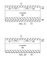
A surface layer of oxide 318 may grow on the backside nitride layer 312 prior to deposition of the encapsulating diffusion barrier silicon nitride layer 316 (FIG. 3B ). When this occurs, a short dilHF deglaze may be required after the diffusion barrier nitride layer 316 is stripped, to remove the surface oxide 318 and to ensure complete stripping of the backside silicon nitride layer 312. About 15 nm of the topside oxide layer 304 may be etched away by the short dilHF deglaze. The change in thickness of the topside oxide layer 304 may cause problems for subsequent process steps. For example, during a photolithography step, reflections may be sensitive to the thickness of the topside oxide layer 304.
In step 404 (illustrated in FIG. 3B ) a diffusion barrier silicon nitride layer 316 that is described hereinabove is deposited. Typically the diffusion barrier silicon nitride layer 316 is deposited using LPCVD with a recipe optimized to improve across wafer thickness uniformity and to reduce or eliminate diffusion barrier silicon nitride layer 316 defects.
The diffusion barrier silicon nitride layer 316 may be deposited with a thickness in the range of about 30 nm to 80 nm. More preferably the diffusion barrier silicon nitride layer 316 may be deposited with a thickness in the range of about 40 nm to 60 nm. In an example solution the diffusion barrier silicon nitride layer 316 is deposited with a thickness of about 50 nm.
In step 406 the encapsulated semiconductor wafer 300 is annealed at a high temperature equal to or greater than 1000° C.
In step 408 the encapsulating diffusion barrier silicon nitride layer 316 is stripped.
If needed, in step 410 a dilHF deglaze may be performed to remove surface oxide 318 from the backside silicon nitride layer 312. As is illustrated in the cross section in FIG. 3C , the compensation oxide layer 314 may also be etched away during this dilHF deglaze step.
In step 412 an additional dilH3PO4 strip is performed to remove the backside silicon nitride layer 312. The cross section in FIG. 3D shows semiconductor wafer 300 after completion of the backside silicon nitride layer 312 strip.
The semiconductor wafer is now ready for further processing in step 414.
An additional benefit of depositing and removing the diffusion barrier silicon nitride layer 316 is that the semiconductor wafer 300 has significantly fewer particles and defects than semiconductor wafers that go through the high temperature anneal without the diffusion barrier silicon nitride layer 316. This aspect of the embodiment methods results in higher integrated circuit yield.
Modifications are possible in the described embodiments, and other embodiments are possible within the scope of the claims.
Claims (20)
1. A method, comprising:
depositing a diffusion barrier layer that encapsulates a semiconductor wafer, the semiconductor wafer having a silicon nitride layer on a backside of the semiconductor wafer and with a silicon dioxide layer on a topside of the semiconductor wafer;
after depositing the diffusion barrier layer, annealing the semiconductor wafer at a temperature greater than or equal to about 1000° C.;
after the annealing, stripping the diffusion barrier layer; and
stripping the silicon nitride layer.
2. The method of claim 1 , in which the diffusion barrier layer is a silicon nitride layer with a thickness between about 30 nm and 80 nm.
3. The method of claim 1 , in which the diffusion barrier layer is a silicon nitride layer with a thickness between about 40 nm and 60 nm.
4. The method of claim 1 , in which the diffusion barrier layer is a silicon nitride layer with a thickness of about 50 nm.
5. The method of claim 1 , in which the diffusion barrier layer is a silicon nitride layer deposited using LPCVD with a NH3 to SiH2Cl2 flow rate ratio of about 10:1; with a NH3 flow rate of about 600 sccm; a deposition pressure of about 300 mTorr; a deposition temperature of about 700° C.; and a deposition rate of about 0.67 nm/min.
6. The method of claim 1 , further including performing a dilute HF deglaze prior to stripping the diffusion barrier layer.
7. The method of claim 1 , further including performing a dilute HF deglaze after stripping the diffusion barrier layer and before stripping the backside silicon nitride layer.
8. The method of claim 1 , in which the diffusion barrier layer is a silicon nitride layer or a silicon oxynitride layer.
9. The method of claim 8 in which the diffusion barrier silicon nitride layer and the backside silicon nitride layer are stripped with hot phosphoric acid.
10. The method of claim 1 , further comprising increasing a thickness of the silicon dioxide layer on the topside of the semiconductor wafer prior to depositing the diffusion barrier layer.
11. The method of claim 10 , in which the thickness of the silicon dioxide layer is increased by between about 10 nm to 20 nm.
12. The method of claim 10 , in which the thickness of the silicon dioxide layer is increased by about 15 nm.
13. A method, comprising:
depositing a diffusion barrier layer that encapsulates a semiconductor wafer with a silicon nitride layer on a backside of the semiconductor wafer and with a silicon dioxide layer on a topside of the semiconductor wafer;
annealing the semiconductor wafer at a temperature greater than or equal to about 1000° C.;
stripping the diffusion barrier layer; and
stripping the silicon nitride layer, in which the diffusion barrier layer is a silicon nitride layer deposited using LPCVD with a NH3 to SiH2Cl2 flow rate ratio of about 10:1; with a NH3 flow rate between about 600 sccm and 1200 sccm; a deposition pressure in a range of about 200 mTorr to about 300 mTorr; a deposition temperature between about 695° C. to about 715° C.; and a deposition rate between about 0.60 nm/min to about 0.75 nm/min.
14. A method, comprising:
increasing a thickness of a silicon dioxide layer on a topside of a semiconductor wafer;
depositing a silicon nitride or silicon oxynitride diffusion barrier layer that encapsulates the semiconductor wafer;
annealing the encapsulated semiconductor wafer at a temperature greater than or equal to 1000° C.;
after the annealing, deglazing the silicon nitride or silicon oxynitride diffusion barrier layer using dilute hydrofluoric acid;
stripping the diffusion barrier silicon nitride layer or the diffusion barrier silicon oxynitride layer; and
stripping the silicon nitride layer on a backside of the semiconductor wafer.
15. The method of claim 14 , in which the thickness of the silicon dioxide layer is increased by 10 nm to 20 nm prior to depositing the silicon nitride or silicon oxynitride diffusion barrier layer.
16. The method of claim 14 , in which the thickness of the silicon dioxide layer is increased by a thickness in a range of about 10 nm to about 20 nm prior to depositing the silicon nitride or silicon oxynitride diffusion barrier layer.
17. The method of claim 14 , further including a dilute HF deglaze prior to stripping the silicon nitride on the backside of the semiconductor wafer.
18. The method of claim 14 , in which the diffusion barrier is a silicon nitride layer deposited using LPCVD with a NH3 to SiH2Cl2 flow rate ratio of about 10:1; with a NH3 flow rate between about 600 sccm to about 1200 sccm; a deposition pressure in a range of about 200 mTorr to about 300 mTorr; a deposition temperature between about 695° C. and about 715° C.; and a deposition rate between about 0.60 nm/min to about 0.75 nm/min.
19. The method of claim 14 , in which the diffusion barrier is a silicon nitride layer deposited using LPCVD with a NH3 to SiH2Cl2 flow rate ratio of about 10:1; with a NH3 flow rate of about 600 sccm; a deposition pressure of about 300 mTorr; a deposition temperature of about 700° C.; and a deposition rate of about 0.67 nm/min.
20. The method of claim 14 , in which the silicon nitride layer and the diffusion barrier silicon nitride layer or diffusion barrier silicon oxynitride layer are subsequently stripped using hot phosphoric acid.
Priority Applications (1)
| Application Number | Priority Date | Filing Date | Title |
|---|---|---|---|
| US15/379,251 US10068769B2 (en) | 2016-12-14 | 2016-12-14 | Methods and apparatus for preventing counter-doping during high temperature processing |
Applications Claiming Priority (1)
| Application Number | Priority Date | Filing Date | Title |
|---|---|---|---|
| US15/379,251 US10068769B2 (en) | 2016-12-14 | 2016-12-14 | Methods and apparatus for preventing counter-doping during high temperature processing |
Publications (2)
| Publication Number | Publication Date |
|---|---|
| US20180166280A1 US20180166280A1 (en) | 2018-06-14 |
| US10068769B2 true US10068769B2 (en) | 2018-09-04 |
Family
ID=62490288
Family Applications (1)
| Application Number | Title | Priority Date | Filing Date |
|---|---|---|---|
| US15/379,251 Active US10068769B2 (en) | 2016-12-14 | 2016-12-14 | Methods and apparatus for preventing counter-doping during high temperature processing |
Country Status (1)
| Country | Link |
|---|---|
| US (1) | US10068769B2 (en) |
Families Citing this family (1)
| Publication number | Priority date | Publication date | Assignee | Title |
|---|---|---|---|---|
| US11205575B2 (en) * | 2019-04-24 | 2021-12-21 | Texas Instruments Incorporated | Method for stripping one or more layers from a semiconductor wafer |
Citations (4)
| Publication number | Priority date | Publication date | Assignee | Title |
|---|---|---|---|---|
| US20070259528A1 (en) * | 2004-10-06 | 2007-11-08 | Commissariat A L'energie Atomique | Method for Providing Mixed Stacked Structures, with Various Insulating Zones and/or Electrically Conductiong Zones Vertically Localized |
| US20110201172A1 (en) * | 2010-02-17 | 2011-08-18 | Taiwan Semiconductor Manufacturing Company, Ltd. | Method for fabricating a semiconductor device |
| US20140213016A1 (en) * | 2013-01-30 | 2014-07-31 | Applied Materials, Inc. | In situ silicon surface pre-clean for high performance passivation of silicon solar cells |
| US20150279941A1 (en) * | 2010-09-30 | 2015-10-01 | Infineon Technologies Ag | Composite Wafer Having a Graphite Core |
-
2016
- 2016-12-14 US US15/379,251 patent/US10068769B2/en active Active
Patent Citations (4)
| Publication number | Priority date | Publication date | Assignee | Title |
|---|---|---|---|---|
| US20070259528A1 (en) * | 2004-10-06 | 2007-11-08 | Commissariat A L'energie Atomique | Method for Providing Mixed Stacked Structures, with Various Insulating Zones and/or Electrically Conductiong Zones Vertically Localized |
| US20110201172A1 (en) * | 2010-02-17 | 2011-08-18 | Taiwan Semiconductor Manufacturing Company, Ltd. | Method for fabricating a semiconductor device |
| US20150279941A1 (en) * | 2010-09-30 | 2015-10-01 | Infineon Technologies Ag | Composite Wafer Having a Graphite Core |
| US20140213016A1 (en) * | 2013-01-30 | 2014-07-31 | Applied Materials, Inc. | In situ silicon surface pre-clean for high performance passivation of silicon solar cells |
Also Published As
| Publication number | Publication date |
|---|---|
| US20180166280A1 (en) | 2018-06-14 |
Similar Documents
| Publication | Publication Date | Title |
|---|---|---|
| US20060237766A1 (en) | Semiconductor device using solid phase epitaxy and method for fabricating the same | |
| US20090001418A1 (en) | Semiconductor device and method for fabricating the same | |
| US7514337B2 (en) | Semiconductor device using EPI-layer and method of forming the same | |
| US7972922B2 (en) | Method of forming a semiconductor layer | |
| CN108022841B (en) | Method for manufacturing semiconductor device | |
| US5789308A (en) | Manufacturing method for wafer slice starting material to optimize extrinsic gettering during semiconductor fabrication | |
| US9287264B1 (en) | Epitaxially grown silicon germanium channel FinFET with silicon underlayer | |
| US8883033B2 (en) | Method for removing nitride material | |
| US6432786B2 (en) | Method of forming a gate oxide layer with an improved ability to resist the process damage | |
| US20160372463A1 (en) | High quality deep trench oxide | |
| US20190214254A1 (en) | SiGe FINS FORMED ON A SUBSTRATE | |
| US10068769B2 (en) | Methods and apparatus for preventing counter-doping during high temperature processing | |
| US7470961B2 (en) | Semiconductor device and method of manufacturing the same | |
| KR100966002B1 (en) | Methods of etching nickel silicide and cobalt silicide and methods of forming conductive lines | |
| US20120142159A1 (en) | Method for fabricating semiconductor device | |
| US8928047B2 (en) | MOSFET with source side only stress | |
| US9741818B2 (en) | Manufacturing method of semiconductor structure for improving quality of epitaxial layers | |
| US10192791B1 (en) | Semiconductor devices with robust low-k sidewall spacers and method for producing the same | |
| US6503814B2 (en) | Method for forming trench isolation | |
| US20140220756A1 (en) | Methods of forming semiconductor devices by forming a semiconductor layer above source/drain regions prior to removing a gate cap layer | |
| JP2014140025A (en) | Semiconductor device manufacturing method | |
| US9722045B2 (en) | Buffer layer for modulating Vt across devices | |
| TW201717281A (en) | Semiconductor device and method for fabricating the same | |
| US20060024938A1 (en) | Method for reducing metal silicide excessive encroachment defects in the manufacture of a semiconductor device having silicided source/drain regions | |
| KR100607799B1 (en) | Method for forming the gate oxide of semiconductor device |
Legal Events
| Date | Code | Title | Description |
|---|---|---|---|
| AS | Assignment |
Owner name: TEXAS INSTRUMENTS INCORPORATED, TEXAS Free format text: ASSIGNMENT OF ASSIGNORS INTEREST;ASSIGNORS:DEV, PRAKASH DALPATBHAI;WANG, FUCHAO;KUSEK, NICHOLAS ANDREW;REEL/FRAME:040737/0907 Effective date: 20161207 |
|
| STCF | Information on status: patent grant |
Free format text: PATENTED CASE |
|
| MAFP | Maintenance fee payment |
Free format text: PAYMENT OF MAINTENANCE FEE, 4TH YEAR, LARGE ENTITY (ORIGINAL EVENT CODE: M1551); ENTITY STATUS OF PATENT OWNER: LARGE ENTITY Year of fee payment: 4 |