US10042226B2 - Display device - Google Patents
Display device Download PDFInfo
- Publication number
- US10042226B2 US10042226B2 US15/422,986 US201715422986A US10042226B2 US 10042226 B2 US10042226 B2 US 10042226B2 US 201715422986 A US201715422986 A US 201715422986A US 10042226 B2 US10042226 B2 US 10042226B2
- Authority
- US
- United States
- Prior art keywords
- source line
- connection portion
- display device
- semiconductor layer
- region
- Prior art date
- Legal status (The legal status is an assumption and is not a legal conclusion. Google has not performed a legal analysis and makes no representation as to the accuracy of the status listed.)
- Active
Links
Images


Classifications
-
- G—PHYSICS
- G02—OPTICS
- G02F—OPTICAL DEVICES OR ARRANGEMENTS FOR THE CONTROL OF LIGHT BY MODIFICATION OF THE OPTICAL PROPERTIES OF THE MEDIA OF THE ELEMENTS INVOLVED THEREIN; NON-LINEAR OPTICS; FREQUENCY-CHANGING OF LIGHT; OPTICAL LOGIC ELEMENTS; OPTICAL ANALOGUE/DIGITAL CONVERTERS
- G02F1/00—Devices or arrangements for the control of the intensity, colour, phase, polarisation or direction of light arriving from an independent light source, e.g. switching, gating or modulating; Non-linear optics
- G02F1/01—Devices or arrangements for the control of the intensity, colour, phase, polarisation or direction of light arriving from an independent light source, e.g. switching, gating or modulating; Non-linear optics for the control of the intensity, phase, polarisation or colour
- G02F1/13—Devices or arrangements for the control of the intensity, colour, phase, polarisation or direction of light arriving from an independent light source, e.g. switching, gating or modulating; Non-linear optics for the control of the intensity, phase, polarisation or colour based on liquid crystals, e.g. single liquid crystal display cells
- G02F1/133—Constructional arrangements; Operation of liquid crystal cells; Circuit arrangements
- G02F1/136—Liquid crystal cells structurally associated with a semi-conducting layer or substrate, e.g. cells forming part of an integrated circuit
- G02F1/1362—Active matrix addressed cells
- G02F1/1368—Active matrix addressed cells in which the switching element is a three-electrode device
-
- G—PHYSICS
- G02—OPTICS
- G02F—OPTICAL DEVICES OR ARRANGEMENTS FOR THE CONTROL OF LIGHT BY MODIFICATION OF THE OPTICAL PROPERTIES OF THE MEDIA OF THE ELEMENTS INVOLVED THEREIN; NON-LINEAR OPTICS; FREQUENCY-CHANGING OF LIGHT; OPTICAL LOGIC ELEMENTS; OPTICAL ANALOGUE/DIGITAL CONVERTERS
- G02F1/00—Devices or arrangements for the control of the intensity, colour, phase, polarisation or direction of light arriving from an independent light source, e.g. switching, gating or modulating; Non-linear optics
- G02F1/01—Devices or arrangements for the control of the intensity, colour, phase, polarisation or direction of light arriving from an independent light source, e.g. switching, gating or modulating; Non-linear optics for the control of the intensity, phase, polarisation or colour
- G02F1/13—Devices or arrangements for the control of the intensity, colour, phase, polarisation or direction of light arriving from an independent light source, e.g. switching, gating or modulating; Non-linear optics for the control of the intensity, phase, polarisation or colour based on liquid crystals, e.g. single liquid crystal display cells
- G02F1/133—Constructional arrangements; Operation of liquid crystal cells; Circuit arrangements
- G02F1/136—Liquid crystal cells structurally associated with a semi-conducting layer or substrate, e.g. cells forming part of an integrated circuit
- G02F1/1362—Active matrix addressed cells
- G02F1/136209—Light shielding layers, e.g. black matrix, incorporated in the active matrix substrate, e.g. structurally associated with the switching element
-
- G—PHYSICS
- G02—OPTICS
- G02F—OPTICAL DEVICES OR ARRANGEMENTS FOR THE CONTROL OF LIGHT BY MODIFICATION OF THE OPTICAL PROPERTIES OF THE MEDIA OF THE ELEMENTS INVOLVED THEREIN; NON-LINEAR OPTICS; FREQUENCY-CHANGING OF LIGHT; OPTICAL LOGIC ELEMENTS; OPTICAL ANALOGUE/DIGITAL CONVERTERS
- G02F1/00—Devices or arrangements for the control of the intensity, colour, phase, polarisation or direction of light arriving from an independent light source, e.g. switching, gating or modulating; Non-linear optics
- G02F1/01—Devices or arrangements for the control of the intensity, colour, phase, polarisation or direction of light arriving from an independent light source, e.g. switching, gating or modulating; Non-linear optics for the control of the intensity, phase, polarisation or colour
- G02F1/13—Devices or arrangements for the control of the intensity, colour, phase, polarisation or direction of light arriving from an independent light source, e.g. switching, gating or modulating; Non-linear optics for the control of the intensity, phase, polarisation or colour based on liquid crystals, e.g. single liquid crystal display cells
- G02F1/133—Constructional arrangements; Operation of liquid crystal cells; Circuit arrangements
- G02F1/136—Liquid crystal cells structurally associated with a semi-conducting layer or substrate, e.g. cells forming part of an integrated circuit
- G02F1/1362—Active matrix addressed cells
- G02F1/136227—Through-hole connection of the pixel electrode to the active element through an insulation layer
-
- G—PHYSICS
- G02—OPTICS
- G02F—OPTICAL DEVICES OR ARRANGEMENTS FOR THE CONTROL OF LIGHT BY MODIFICATION OF THE OPTICAL PROPERTIES OF THE MEDIA OF THE ELEMENTS INVOLVED THEREIN; NON-LINEAR OPTICS; FREQUENCY-CHANGING OF LIGHT; OPTICAL LOGIC ELEMENTS; OPTICAL ANALOGUE/DIGITAL CONVERTERS
- G02F1/00—Devices or arrangements for the control of the intensity, colour, phase, polarisation or direction of light arriving from an independent light source, e.g. switching, gating or modulating; Non-linear optics
- G02F1/01—Devices or arrangements for the control of the intensity, colour, phase, polarisation or direction of light arriving from an independent light source, e.g. switching, gating or modulating; Non-linear optics for the control of the intensity, phase, polarisation or colour
- G02F1/13—Devices or arrangements for the control of the intensity, colour, phase, polarisation or direction of light arriving from an independent light source, e.g. switching, gating or modulating; Non-linear optics for the control of the intensity, phase, polarisation or colour based on liquid crystals, e.g. single liquid crystal display cells
- G02F1/133—Constructional arrangements; Operation of liquid crystal cells; Circuit arrangements
- G02F1/136—Liquid crystal cells structurally associated with a semi-conducting layer or substrate, e.g. cells forming part of an integrated circuit
- G02F1/1362—Active matrix addressed cells
- G02F1/136286—Wiring, e.g. gate line, drain line
-
- H01L29/42384—
-
- H—ELECTRICITY
- H10—SEMICONDUCTOR DEVICES; ELECTRIC SOLID-STATE DEVICES NOT OTHERWISE PROVIDED FOR
- H10D—INORGANIC ELECTRIC SEMICONDUCTOR DEVICES
- H10D30/00—Field-effect transistors [FET]
- H10D30/60—Insulated-gate field-effect transistors [IGFET]
- H10D30/67—Thin-film transistors [TFT]
- H10D30/6729—Thin-film transistors [TFT] characterised by the electrodes
- H10D30/673—Thin-film transistors [TFT] characterised by the electrodes characterised by the shapes, relative sizes or dispositions of the gate electrodes
- H10D30/6733—Multi-gate TFTs
-
- H—ELECTRICITY
- H10—SEMICONDUCTOR DEVICES; ELECTRIC SOLID-STATE DEVICES NOT OTHERWISE PROVIDED FOR
- H10D—INORGANIC ELECTRIC SEMICONDUCTOR DEVICES
- H10D30/00—Field-effect transistors [FET]
- H10D30/60—Insulated-gate field-effect transistors [IGFET]
- H10D30/67—Thin-film transistors [TFT]
- H10D30/674—Thin-film transistors [TFT] characterised by the active materials
-
- H—ELECTRICITY
- H10—SEMICONDUCTOR DEVICES; ELECTRIC SOLID-STATE DEVICES NOT OTHERWISE PROVIDED FOR
- H10D—INORGANIC ELECTRIC SEMICONDUCTOR DEVICES
- H10D30/00—Field-effect transistors [FET]
- H10D30/60—Insulated-gate field-effect transistors [IGFET]
- H10D30/67—Thin-film transistors [TFT]
- H10D30/6757—Thin-film transistors [TFT] characterised by the structure of the channel, e.g. transverse or longitudinal shape or doping profile
-
- H—ELECTRICITY
- H10—SEMICONDUCTOR DEVICES; ELECTRIC SOLID-STATE DEVICES NOT OTHERWISE PROVIDED FOR
- H10D—INORGANIC ELECTRIC SEMICONDUCTOR DEVICES
- H10D86/00—Integrated devices formed in or on insulating or conducting substrates, e.g. formed in silicon-on-insulator [SOI] substrates or on stainless steel or glass substrates
- H10D86/40—Integrated devices formed in or on insulating or conducting substrates, e.g. formed in silicon-on-insulator [SOI] substrates or on stainless steel or glass substrates characterised by multiple TFTs
- H10D86/441—Interconnections, e.g. scanning lines
-
- H—ELECTRICITY
- H10—SEMICONDUCTOR DEVICES; ELECTRIC SOLID-STATE DEVICES NOT OTHERWISE PROVIDED FOR
- H10D—INORGANIC ELECTRIC SEMICONDUCTOR DEVICES
- H10D86/00—Integrated devices formed in or on insulating or conducting substrates, e.g. formed in silicon-on-insulator [SOI] substrates or on stainless steel or glass substrates
- H10D86/40—Integrated devices formed in or on insulating or conducting substrates, e.g. formed in silicon-on-insulator [SOI] substrates or on stainless steel or glass substrates characterised by multiple TFTs
- H10D86/60—Integrated devices formed in or on insulating or conducting substrates, e.g. formed in silicon-on-insulator [SOI] substrates or on stainless steel or glass substrates characterised by multiple TFTs wherein the TFTs are in active matrices
-
- G—PHYSICS
- G02—OPTICS
- G02F—OPTICAL DEVICES OR ARRANGEMENTS FOR THE CONTROL OF LIGHT BY MODIFICATION OF THE OPTICAL PROPERTIES OF THE MEDIA OF THE ELEMENTS INVOLVED THEREIN; NON-LINEAR OPTICS; FREQUENCY-CHANGING OF LIGHT; OPTICAL LOGIC ELEMENTS; OPTICAL ANALOGUE/DIGITAL CONVERTERS
- G02F1/00—Devices or arrangements for the control of the intensity, colour, phase, polarisation or direction of light arriving from an independent light source, e.g. switching, gating or modulating; Non-linear optics
- G02F1/01—Devices or arrangements for the control of the intensity, colour, phase, polarisation or direction of light arriving from an independent light source, e.g. switching, gating or modulating; Non-linear optics for the control of the intensity, phase, polarisation or colour
- G02F1/13—Devices or arrangements for the control of the intensity, colour, phase, polarisation or direction of light arriving from an independent light source, e.g. switching, gating or modulating; Non-linear optics for the control of the intensity, phase, polarisation or colour based on liquid crystals, e.g. single liquid crystal display cells
- G02F1/133—Constructional arrangements; Operation of liquid crystal cells; Circuit arrangements
- G02F1/136—Liquid crystal cells structurally associated with a semi-conducting layer or substrate, e.g. cells forming part of an integrated circuit
- G02F1/1362—Active matrix addressed cells
- G02F1/1368—Active matrix addressed cells in which the switching element is a three-electrode device
- G02F1/13685—Top gates
-
- G02F2001/13685—
-
- H—ELECTRICITY
- H10—SEMICONDUCTOR DEVICES; ELECTRIC SOLID-STATE DEVICES NOT OTHERWISE PROVIDED FOR
- H10D—INORGANIC ELECTRIC SEMICONDUCTOR DEVICES
- H10D30/00—Field-effect transistors [FET]
- H10D30/60—Insulated-gate field-effect transistors [IGFET]
- H10D30/67—Thin-film transistors [TFT]
- H10D30/6704—Thin-film transistors [TFT] having supplementary regions or layers in the thin films or in the insulated bulk substrates for controlling properties of the device
- H10D30/6723—Thin-film transistors [TFT] having supplementary regions or layers in the thin films or in the insulated bulk substrates for controlling properties of the device having light shields
Definitions
- Embodiments described herein relate generally to a display device.
- Display devices such as liquid crystal displays and organic electroluminescence (EL) display devices comprise various wiring lines including gate lines, source lines, etc. which are connected to switching elements and the like, which drive pixels.
- EL organic electroluminescence
- the width of the lines is reduced, which also creates a tendency of increasing the electric resistance of the wiring lines.
- FIG. 1 is a circuit diagram schematically showing an example of a display device according to the first embodiment.
- FIG. 2 is a plan view showing an example of a wiring pattern of the display device according to the first embodiment.
- FIG. 3 is a plan view showing a pattern of a light-shielding film of the display device according to the first embodiment.
- FIG. 4 is a cross section taken along line IV-IV in FIG. 2 .
- FIG. 5 is an enlarged view of a connection section of a gate line and a gate driver in the display device according to the first embodiment.
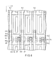
- FIG. 6 is a plan view showing an example of a wiring pattern of a display device according to the second embodiment.
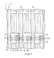
- FIG. 7 is a plan view showing an example of a wiring pattern of a display device according to the third embodiment.
- a display device comprises first and second source lines arranged along a first direction, a gate line including first and second portions arranged along a second direction intersecting the first direction and a connection portion which connects the first portion and the second portion to each other, and a semiconductor layer which intersects at least one of the first portion and the connection portion, each of the first portion and the second portion intersects the first and second source lines, and the connection portion is located between the first source line and the second source line.
- a display device comprises first, second and third source lines arranged along a first direction, and a gate line including first and second portions arranged along a second direction intersecting the first direction and a first connection portion and a second connection portion which connect the first portion and the second portion to each other, the first connection portion is located between the first source line and the second source line, and the second connection portion is located between the second source line and the third source line.
- FIG. 1 is a circuit diagram schematically showing an example of a display device DSP 1 according to the first embodiment.
- the display device is a liquid crystal display device comprising a liquid crystal layer.
- the display device DSP 1 may be any type of display device including a self-luminous display device such as an organic electroluminescence (EL) display device, or an electronic paper display device comprising an electrophoretic element.
- EL organic electroluminescence
- the display device DSP 1 comprises an active-matrix-type display panel PNL and a driving unit which supplies signals for displaying images on the display panel PNL.
- the display panel PNL is, for example, a liquid crystal display panel which holds a liquid crystal layer between a pair of substrates.
- the display panel PNL includes a display area DA where images are displayed.
- the display area DA comprises a plurality of pixels PX arrayed in a matrix.
- the display panel PNL comprises, in the display area DA, a plurality of gate lines GL (GL 1 to GLm) for selecting respective pixels PX, a plurality of source line SL (SL 1 to SLn) for supplying image signals to the respective pixels PX, a common line CL which supplies a common potential (VCOM) to a common electrode CE, which will be described later.
- m and n represent positive integers.
- the driving unit comprises gate drivers GD, a source driver SD and a control circuit CNT.
- the gate drivers GD and the source driver SD are at least partially formed in the display panel PNL.
- the control circuit CNT is provided in a drive IC chip, a flexible printed circuit board (not shown) or the like, which are mounted in the display panel PNL.
- Each of the gate lines G is drawn to the outside of the display area DA and is electrically connected to a respective gate driver GD.
- Each of the source lines SL is drawn to the outside of the display area DA and is electrically connected to the source driver SD.
- Peripheral circuits such as the gate drivers GD and source driver SD each comprise an N-type thin-film transistor, a P-type thin-film transistor, a complementary-type thin-film transistor in which an N type and a P type are combined, or the like, though will not be described in detail.
- Each pixel PX comprises a switching element SW, a pixel electrode PE, a common electrode CE, etc.
- the switching element SW is formed from, for example, an N-type thin-film transistor.
- the switching element SW comprises a gate electrode GE, a source electrode SE and a drain electrode DE.
- the gate electrode GE is connected to the respective gate line GL.
- the source electrode SE is connected to the respective source line SL.
- the drain electrode DE is connected to the respective pixel electrode PE.
- a capacitance is formed between each of the pixel electrode PE and the common electrode CE, and thus an image signal (voltage) necessary for display on each respective pixel PX is retained therein.
- the common electrode CE is connected to the control circuit CNT via the common line CL. Note that the example illustrated is described in connection with the case where a common potential is supplied from the control circuit CNT to the common electrode CE, but the embodiment is not limited to this example. Besides the control circuit CNT, there may be a drive circuit which supplies the common potential.
- the control circuit CNT generates various signals necessary to display images in the display area DA based on an external signal supplied from an external signal source, and outputs them to each of the gate driver GD and the source driver. Further, the control circuit CNT applies a common potential (VCOM) to the common electrode CE.
- VCOM common potential
- the gate driver GD supplies a scanning signal to each of the gate lines GL.
- the source driver SD supplies an image signal to each of the source lines SL.
- the switching elements SW connected to the same gate line GL are switched over between the connection and non-connection states based on the scanning signal supplied to the respective gate line GL.
- the image signal supplied to a source line SL when the switching element SW is in the connection state is supplied to the respective pixel electrode PE through the respective switching element SW.
- an electric field is produced according to the potential difference between the pixel electrode PE and the common electrode CE. Alignment of the liquid crystal molecules contained in the liquid crystal layer is controlled by the electric field produced between the pixel electrode PE and the common electrode CE.
- An image signal written in a pixel PX is held by the capacitance between the respective pixel electrode PE and common electrode CE until the following image signal is written therein.
- the display panel PNL of this embodiment may be of a transmissive type having a transmissive display function, displays images by selectively transmitting light from its rear side, a reflective type having a reflective display function, which displays images by selectively reflecting light from the front side, or a trans-reflective type having both the transmissive display function and the reflective display function.
- the display panel PNL may have such a structure that corresponds to a display mode using a lateral electric field along a main surface of the substrate, a display mode which uses a vertical electric field perpendicular to the main surface of the substrate, a display mode using an oblique electric field inclined to the main surface of the substrate, or a display mode using a combination of these.
- a display mode using a lateral electric field such a structure is applicable, that both the pixel electrode PE and the common electrode CE are provided on one substrate which constitutes the display panel PNL.
- the display mode using a vertical electric field or an oblique electric field such a structure is applicable, that the pixel electrode PE is provided on one substrate constitutes the display panel PNL, and the common electrode CE is provided on the other substrate.
- FIG. 2 is a plan view partially showing an example of the pixel pattern of the display panel PNL shown in FIG. 1 .
- a plan view of an array substrate AR which is one substrate which constitutes the display panel PNL, is shown.
- the first direction X and the Y second direction intersect each other.
- the first direction X and the second direction Y intersect at right angles in this example, but they may intersect at an angle other than 90 degrees.
- the main surface of the substrate is a surface parallel to an X-Y plane defined by the first direction X and the second direction Y.
- FIG. 2 shows only the principal part of three pixels PX arranged along the first direction X, and illustration of the insulating film, common electrode, light-shielding film, etc. is omitted.
- the pixel PX illustrated here has a rectangular shape with short sides along the first direction X and long sides along the second direction Y.
- the shape of the pixel PX is not limited to rectangular, but may be changed as needed.
- the array substrate AR comprises a gate line GL, source lines SL 1 to SL 3 , switching elements SW, pixel electrodes PE, etc.
- the gate line GL is formed into a ladder shape. More specifically, the gate line GL includes a first portion GLa, a second portion GLb and a connection portion GLc.
- the first portion GLa and the second portion GLb each have substantially a fixed width therealong, and are extended in the first direction X.
- the first portion GLa and the second portion GLb are arranged along the second direction Y.
- the first portion GLa is located on a side more close to the pixel electrode PE than to the second portion GLb.
- the first portion GLa includes the first gate electrode WG 1 and the second gate electrode WG 2 of the respective switching element SW.
- the connection portion GLc is extended along the second direction Y in each pixel PX and connects the first portion GLa and the second portion GLb to each other.
- the source lines SL 1 to SL 3 are each extended along the second direction Y and arranged along the first direction X.
- the source lines SL 1 to SL 3 each intersect the first portion GLa and the second portion GLb.
- the connection portion GLc is located between an adjacent pair of source lines SL. In other words, the connection portions GLc and the source lines SL are arranged alternately along the first direction X.
- the source lines SL and the gate lines GL are each extended linearly, but they may be bent.
- the pixel electrodes PE are arranged in a matrix along the first direction X and the second direction Y.
- the first portion GLa and the second portion GLb are located between two adjacent pixel electrodes PE along the second direction Y.
- An interval L 1 between the first portion GLa and the second portion GLb along the second direction Y is less than a length L 2 of the pixel electrode PE along the second direction Y.
- no pixel electrode PE intervenes between the first portion GLa and the second portion GLb.
- the connection portion GLc is located between two adjacent pixel electrodes PE along the second direction Y.
- the gate line GL includes an opening OP elongated along in the first direction X between two adjacent connection portions GLc.
- the opening OP has a rectangular shape.
- a pitch PGLc of the connection portions GLc is equal to a pitch PSL of the source lines SL.
- the pitch PGLc of the connection portions GLc is equivalent to a distance between the centers of two adjacent connection portions GLc along the first direction X.
- the pitch PSL of the source lines SL is equivalent to a distance between the centers of two adjacent source lines SL along the first direction X.
- the three pixels PX illustrated are identical to each other in configuration, and therefore, the configuration thereof will be described in detail by focusing the pixel PX located between the source lines SL 1 and SL 2 .
- the switching element SW is arranged near the intersection of the first portion GLa of the gate line GL and the source line SL 1 .
- the switching element SW is a double-gate thin film transistor including the first gate electrode WG 1 and the second gate electrode WG 2 . That is, the semiconductor layer SC which constitutes the switching element SW includes two regions which overlap the first portion GLa of the gate line GL.
- the semiconductor layer SC is formed into, approximately, a U-letter shape, and includes a first region SC 1 , a second region SC 2 and a third region SC 3 .
- the first region SC 1 is extended along the second direction Y under the source line SL 1 and intersects the first portion GLa, but does not intersect the second portion GLb.
- the first region SC 1 is electrically connected to source line SL 1 by its one end side through a contact hole CH 1 , and the other end side is located between the first portion GLa and the second portion GLb.
- the first gate electrode WG 1 is equivalent to the region of the first portion GLa, which intersects the first region SC 1 .
- the second region SC 2 is extended along the second direction Y from between source line SL 1 and the connection portion GLc toward the pixel electrode PE and intersects the first portion GLa, but does not intersect the second portion GLb.
- One end side of the second region SC 2 is expanded and electrically connected to the pixel electrode PE through a contact hole CH 2 and a relay electrode RE, and the other end side is located between the first portion GLa and the second portion GLb.
- the second gate electrode WG 2 is equivalent to the region of the first portion GLa, which intersects the second region SC 2 .
- the connection portion GLc is located between the second region SC 2 and the source line SL 2 .
- the third region SC 3 is located between the first portion GLa and the second portion GLb, and extended along the first direction X to connect the first region SC 1 and the second region SC 2 to each other.
- the third region SC 3 overlaps the opening OP.
- the pixel electrode PE includes a contact portion PEa and an electrode portion PEb.
- the contact portion PEa overlaps the relay electrode RE and is electrically connected to the relay electrode RE through openings 15 a and 16 a and CEa, which will be explained in detail later.
- the electrode portion PEb is extended from the contact portion PEa along the second direction Y.
- the electrode portion PEb includes a slit opening PEc along the second direction Y.
- the electrode portion PEb may include a plurality of openings PEc, but which may be omitted.
- the width of the first portion GLa is determined by the channel length of the switching element SW.
- the width of the second portion GLb can be determined as needed according to the width of the region which does not overlap the semiconductor layer SC or pixel electrode PE, and can be made greater than that of the first portion GLa.
- expansion of the width of the second portion GLb leads to expansion of the pitch between adjacent pixels PX along the second direction Y, or reduction of the length of the pixel PX along the second direction Y. Under these circumstances, it is preferable to determine the width of the second portion GLb within such an extent to be able to achieve the resistance required as the gate line GL.
- connection portion GLc is provided in one pixel PX, but a plurality of connection portions may be provided as well.
- FIG. 3 is a plan view showing an example of the region in which a light-shielding film BM which partitions into pixels PX is formed.
- a plan view of a counter-substrate CT which is another substrate which constitutes the display panel PNL, is shown. Note that the main part of the array substrate AR shown in FIG. 2 is illustrated with the dotted line.
- the light-shielding film BM is arranged so as to overlap the source line SL, the gate line GL and the switching element SW. Further, the light-shielding film BM is arranged to overlap the contact portion PEa of the pixel electrode PE and partition into the pixels PX. That is, the light-shielding film BM includes an opening AP which exposes the electrode portion PEb of the pixel electrode PE. The opening AP corresponds to the region which substantially contributes to display.
- FIG. 4 is a cross section of the display panel PNL taken along line IV-IV shown in FIG. 2 .
- the display panel PNL comprises the array substrate AR, the counter-substrate CT and the liquid crystal layer LQ.
- the counter-substrate CT opposes the array substrate AR.
- the liquid crystal layer LQ is held between the array substrate AR and the counter-substrate CT.
- the array substrate AR comprises a first insulating substrate 10 , a light-shielding layer 11 , first to fifth insulating films 12 to 16 , a switching element SW, a common electrode CE, a pixel electrode PE, a first alignment film AL 1 , and the like.
- the first insulating substrate 10 is formed from, for example, an insulating material such as glass or resin.
- the light-shielding layer 11 is formed on the first insulating substrate 10 .
- the light-shielding layer 11 shields light towards the semiconductor layer SC from the backlight unit (not shown).
- the first insulating film 12 is formed to cover the light-shielding layer 11 and also on the first insulating substrate 10 .
- the semiconductor layer SC which constitutes the switching element SW, is formed on the first insulating film 12 .
- the semiconductor layer SC is formed from, for example, polycrystalline silicon.
- the semiconductor layer SC may be formed from, for example, some other silicon-based material such as amorphous silicon, or an oxide semiconductor containing an oxide of at least one of indium (In), gallium (Ga), zinc (Zn) and tin (Sn), for example.
- the semiconductor layer SC is formed of an oxide semiconductor, the light-shielding layer 11 may be omitted.
- the second insulating film 13 is formed to cover the semiconductor layer SC and also on the first insulating film 12 .
- the first gate electrode WG 1 and the second gate electrode WG 2 are formed on the second insulating film 13 .
- the light-shielding layer 11 should preferably be located in a region directly under the semiconductor layer SC, which opposes the first gate electrode WG 1 and the second gate electrode WG 2 .
- the third insulating film 14 is formed to cover the first gate electrode WG 1 and the second gate electrode WG 2 and also on the second insulating film 13 .
- the first to third insulating films 12 to 14 are formed from, for example, an inorganic insulating material such as silicon oxide or silicon nitride.
- the source line SL 1 and the relay electrode RE are formed on the third insulating film 14 .
- the source line SL 1 is connected to one end portion of the semiconductor layer SC via the contact hole CH 1 made through the third insulating film 14 and the second insulating film 13 .
- the relay electrode RE is connected to the other end portion of the semiconductor layer SC via the contact hole CH 2 made through the third insulating film 14 and the second insulating film 13 .
- the fourth insulating film 15 is formed to cover the source line SL 1 and the relay electrode RE and also on the third insulating film 14 .
- An opening 15 a is formed in a region of the fourth insulating film 15 , which overlaps the relay electrode RE.
- the fourth insulating film 15 is formed of, for example, an organic insulating material such as a transmissive resin.
- the common electrode CE is formed on the fourth insulating film 15 .
- the common electrode CE includes an opening CEa.
- the opening CEa is formed above the opening 15 a and has a size slightly greater than that of the opening 15 a.
- the fifth insulating film 16 is formed to cover the common electrode CE and also on the fourth insulating film 15 .
- the fifth insulating film 16 is formed of, for example, silicon nitride.
- an opening 16 a is formed in the fifth insulating film 16 , so as to expose the relay electrode RE.
- the pixel electrode PE is formed on the fifth insulating film 16 , a portion of the pixel electrode PE which is formed in the opening 16 a is connected with the relay electrode RE.
- the fifth insulating film 16 and the pixel electrode PE are covered by the first alignment film AL 1 .
- the counter-substrate CT comprises a second insulating substrate 20 , a light-shielding film BM, a color filter 21 , an overcoat layer 22 , a second alignment film AL 2 and the like.
- the second insulating substrate 20 is formed from, for example, an insulating material such as glass or resin.
- the light-shielding layer BM is formed on an inner surface 20 A of the second insulating substrate 20 , which opposes the array substrate AR, and partitions into pixels PX as described with reference to FIG. 3 .
- the color filter 21 is formed on the inner surface 20 A and partially overlaps the light-shielding layer BM.
- the color filter 21 is disposed on the opening OP of each pixel PX shown in FIG. 3 .
- the color filter 21 is formed of a resin material colored in red, green, blue or the like.
- the overcoat layer 22 covers the color filter 21 .
- the overcoat layer 22 is formed of a transparent resin material.
- the overcoat layer 22 is covered by the second alignment film AL 2 .
- the array substrate AR and the counter-substrate CT configured as described above are arranged so that the first alignment film AL 1 and the second alignment film AL 2 oppose each other and attached each other with a sealing material (not shown).
- a liquid crystal composition containing liquid crystal molecules is sealed between the first alignment film AL 1 of the array substrate AR and the second alignment film AL 2 of the counter-substrate CT, thus forming a liquid crystal layer LQ.
- the first alignment film AL 1 and the second alignment film AL 2 are subjected to an alignment treatment to be aligned in the same direction in a plane parallel to the main surfaces of the first insulating substrate 10 and the second insulating substrate 20 . Therefore, in a state where an electric field is not formed between the pixel electrode PE and the common electrode CE, the liquid crystal molecules contained in the liquid crystal layer LQ are set in an initial alignment in an alignment direction of the first alignment film AL 1 and the second alignment film AL 2 . On the other hand, in a state where an electric field is formed between the pixel electrode PE and the common electrode CE, the liquid crystal molecules are aligned in a direction different from that of the initial alignment.
- FIG. 5 is an enlarged view of the region where the gate driver GD and the gate line GL are connected to each other.
- the gate lines GL are formed into a ladder shape including a first portion GLa, a second portion GLb and a connection portion GLc, in the display area DA.
- the gate lines GL each include an end GLE connected to the gate driver GD in a non-display area NDA on an outer side of the display area DA.
- the end GLE may not necessarily be of the same shape as that of the display area DA, but may be formed into a belt-like shape as in the example illustrated.
- a width W 3 of the end GLE along the second direction Y should be greater than at least the width W 1 of the first portion GLa and also should have a width greater than or equal to a sum of the width W 1 of the first portion GLa and the width W 2 of the second portion GLb.
- the width W 2 is greater than the width W 1 .
- the width W 2 is twice the width W 1 or more.
- a width WOP the opening OP along the second direction Y is greater than the width W 1 .
- the gate lines GL each comprises the first portion GLa, which constitutes the first gate electrode WG 1 and the second gate electrode WG 2 of the switching element SW, and the second portion GLb arranged along side the first portion GLa, and in each pixel PX, the first portion GLa and the second portion GLb are connected to each other with the connection portion GLc.
- the width of the transmission path in the gate line GL which substantially transmits a scanning signal, can be increased and the resistance of the gate line GL can be reduced as compared to the case where the gate line GL is formed linearly only of the first portion GLa. Therefore, even if the signal write time assigned to each gate line GL is shortened, the degradation of the signal, which may be caused by the wiring resistance of the gate lines GL can be suppressed, thereby making it possible to suppress the degradation of display quality.
- the gate lines GL each comprise the first portion GLa and the second portion GLb, the resistance of the gate lines GL can be decreased without increasing the width of the first portion GLa. Therefore, the resistance of the gate lines GL can be decreased without increasing the channel length of the thin film transistor which constitutes the switching element SW.
- the first portion GLa and the second portion GLb of one gate line GL are continuously formed with respect to a plurality of pixels PX arranged along the first direction X. More specifically, the resistance of the gate lines GL as a whole can be lowered as compared to the structure in which the first portion GLa is not continuously formed in a plurality of pixels, for example, that is, the first portion GLa is divided for each pixel, and the second portion GLb is continuously formed with respect to the pixels PX so that the second portion GLb and the first portion GLa are connected with the connection portion GLc in each pixel PX.
- the area of the second portion GLb, required to lower the resistance of the gate lines GL can be decreased.
- the resistance of the gate lines GL can be lowered while fully maintaining the area of the region which contributes to display.
- FIG. 6 is a plan view showing an example of the wiring pattern of a display device DSP 2 according to the second embodiment.
- the second embodiment is different from the first embodiment in that semiconductor layer SC of the switching element SW is formed into substantially an L-letter shape. That is, the semiconductor layer SC intersects each of the first portion GLa of the gate line GL and the connection portion GLc.
- the main differences will be described.
- the semiconductor layer SC includes a first region SC 1 and a fourth region SC 4 .
- the first region SC 1 is extended along the second direction Y under the source line SL 1 , and intersects the first portion GLa as in the first embodiment.
- One end of the first region SC 1 is electrically connected to the source line SL 1 via the contact hole CH 1 .
- the other end of the first region SC 1 is located between the first portion GLa and the second portion GLb.
- the first gate electrode WG 1 of the switching element SW is equivalent to the region of the first portion GLa, which intersects the first region SC 1 .
- the fourth region SC 4 is extended along the first direction X and intersects the connection portion GLc.
- An end of the fourth region SC 4 is connected to the first region SC 1 .
- the other end of the fourth region SC 4 is located between the connection portion GLc and the source line SL 2 and is electrically connected to the pixel electrode PE via the contact hole CH 2 and the relay electrode RE. That is, the relay electrode RE is located in the opening OP.
- the second gate electrode WG 2 of the switching element SW is equivalent to the region of the connection portion GLc, which intersects the fourth region SC 4 .
- the first portion GLa, the second portion GLb and the connection portion GLc are formed to have substantially the same width, but the width of the second portion GLb may be greater than that of the first portion GLa or of the connection portion GLc.
- connection portion CP of the pixel electrode PE and the switching element SW is formed between the connection portion GLc and the source line SL and also between the first portion GLa and the second portion GLb.
- the connection portion CP is provided in the region where the respective gate line GL is formed.
- FIG. 7 is a plan view schematically showing an example of the wiring pattern of a display device DSP 3 according to the third embodiment.
- the third embodiment is different from the above-described first or second embodiment in that the switching element SW is a thin film transistor of a single gate structure.
- the switching element SW is a thin film transistor of a single gate structure.
- the semiconductor layer SC is located between the first portion GLa and the second portion GLb and is extended along the first direction X.
- the semiconductor layer SC intersects only the connection portion GLc between the source lines SL 1 and SL 2 .
- An end of the semiconductor layer SC is located under the source line SL 1 and is electrically connected to the source line SL 1 through the contact hole CH 1 .
- the other end of the semiconductor layer SC is located between the connection portion GLc and source line SL 2 and is electrically connected to the pixel electrode PE via the contact hole CH 2 and the relay electrode RE.
- the gate electrode G of the switching element SW is equivalent to the region of the connection portion GLc, which intersects the semiconductor layer SC.
- the contact hole CH 2 formed in the switching element SW 1 and the contact hole CH 1 formed in the switching element SW 2 adjacent to the switching element SW 1 along the first direction X are located in the opening OP.
Landscapes
- Physics & Mathematics (AREA)
- Nonlinear Science (AREA)
- Engineering & Computer Science (AREA)
- Microelectronics & Electronic Packaging (AREA)
- Mathematical Physics (AREA)
- Chemical & Material Sciences (AREA)
- Crystallography & Structural Chemistry (AREA)
- General Physics & Mathematics (AREA)
- Optics & Photonics (AREA)
- Liquid Crystal (AREA)
- Devices For Indicating Variable Information By Combining Individual Elements (AREA)
- Electroluminescent Light Sources (AREA)
Abstract
Description
Claims (17)
Applications Claiming Priority (2)
| Application Number | Priority Date | Filing Date | Title |
|---|---|---|---|
| JP2016018185A JP2017138403A (en) | 2016-02-02 | 2016-02-02 | Display |
| JP2016-018185 | 2016-02-02 |
Publications (2)
| Publication Number | Publication Date |
|---|---|
| US20170219862A1 US20170219862A1 (en) | 2017-08-03 |
| US10042226B2 true US10042226B2 (en) | 2018-08-07 |
Family
ID=59386600
Family Applications (1)
| Application Number | Title | Priority Date | Filing Date |
|---|---|---|---|
| US15/422,986 Active US10042226B2 (en) | 2016-02-02 | 2017-02-02 | Display device |
Country Status (2)
| Country | Link |
|---|---|
| US (1) | US10042226B2 (en) |
| JP (1) | JP2017138403A (en) |
Families Citing this family (1)
| Publication number | Priority date | Publication date | Assignee | Title |
|---|---|---|---|---|
| CN113471225B (en) * | 2021-09-03 | 2021-11-19 | 北京京东方技术开发有限公司 | Display substrate and display panel |
Citations (7)
| Publication number | Priority date | Publication date | Assignee | Title |
|---|---|---|---|---|
| JPH1184421A (en) | 1997-09-10 | 1999-03-26 | Sharp Corp | Active matrix substrate and liquid crystal panel using the same |
| US20100128192A1 (en) * | 2008-11-25 | 2010-05-27 | Hee-Joon Kim | Liquid crystal display and method of manufacturing the same |
| US20140312351A1 (en) * | 2011-04-28 | 2014-10-23 | Sharp Kabushiki Kaisha | Tft substrate and method for correcting wiring fault on tft substrate |
| US20150198850A1 (en) * | 2012-07-19 | 2015-07-16 | Sharp Kabushiki Kaisha | Liquid crystal display device |
| US20150248030A1 (en) * | 1999-03-26 | 2015-09-03 | Semiconductor Energy Laboratory Co., Ltd. | Method for manufacturing an electrooptical device |
| US9310658B2 (en) * | 2012-12-31 | 2016-04-12 | Lg Display Co., Ltd. | Ultra high resolution liquid crystal display having a compensating thin film transistor at each pixel |
| US20160377918A1 (en) * | 2002-03-01 | 2016-12-29 | Semiconductor Energy Laboratory Co., Ltd. | Liquid Crystal Display Device |
-
2016
- 2016-02-02 JP JP2016018185A patent/JP2017138403A/en active Pending
-
2017
- 2017-02-02 US US15/422,986 patent/US10042226B2/en active Active
Patent Citations (7)
| Publication number | Priority date | Publication date | Assignee | Title |
|---|---|---|---|---|
| JPH1184421A (en) | 1997-09-10 | 1999-03-26 | Sharp Corp | Active matrix substrate and liquid crystal panel using the same |
| US20150248030A1 (en) * | 1999-03-26 | 2015-09-03 | Semiconductor Energy Laboratory Co., Ltd. | Method for manufacturing an electrooptical device |
| US20160377918A1 (en) * | 2002-03-01 | 2016-12-29 | Semiconductor Energy Laboratory Co., Ltd. | Liquid Crystal Display Device |
| US20100128192A1 (en) * | 2008-11-25 | 2010-05-27 | Hee-Joon Kim | Liquid crystal display and method of manufacturing the same |
| US20140312351A1 (en) * | 2011-04-28 | 2014-10-23 | Sharp Kabushiki Kaisha | Tft substrate and method for correcting wiring fault on tft substrate |
| US20150198850A1 (en) * | 2012-07-19 | 2015-07-16 | Sharp Kabushiki Kaisha | Liquid crystal display device |
| US9310658B2 (en) * | 2012-12-31 | 2016-04-12 | Lg Display Co., Ltd. | Ultra high resolution liquid crystal display having a compensating thin film transistor at each pixel |
Also Published As
| Publication number | Publication date |
|---|---|
| JP2017138403A (en) | 2017-08-10 |
| US20170219862A1 (en) | 2017-08-03 |
Similar Documents
| Publication | Publication Date | Title |
|---|---|---|
| US11675241B2 (en) | Display device | |
| KR101906248B1 (en) | Liquid crystal display device | |
| KR102034112B1 (en) | Liquid crystal display device and method of driving the same | |
| KR101204365B1 (en) | Liquid crystal display panel and method of manufacturing the same | |
| US9875699B2 (en) | Display device | |
| US9501960B2 (en) | Display panel | |
| US10209574B2 (en) | Liquid crystal display | |
| US12125855B2 (en) | Display device | |
| US10529293B2 (en) | Display device | |
| KR20140013902A (en) | Display device | |
| US10409127B2 (en) | Display device | |
| US20190392762A1 (en) | Display Device | |
| KR101944363B1 (en) | Liquid crystal display device | |
| KR20180031898A (en) | Display device having common voltage line | |
| US10042226B2 (en) | Display device | |
| KR102878854B1 (en) | Display Panel with Touch Sensing element therein | |
| US20210333651A1 (en) | Display device | |
| US20260026104A1 (en) | Display device | |
| US20250251636A1 (en) | Display substrate and display device | |
| US11221526B2 (en) | Display device and substrate comprising organic insulating layer | |
| US11694647B2 (en) | Display device | |
| KR102921528B1 (en) | Display Panel with Touch Sensing element therein | |
| JP2015004910A (en) | Electro-optical panel and electronic equipment |
Legal Events
| Date | Code | Title | Description |
|---|---|---|---|
| AS | Assignment |
Owner name: JAPAN DISPLAY INC., JAPAN Free format text: ASSIGNMENT OF ASSIGNORS INTEREST;ASSIGNOR:MOCHIZUKI, KAZUHIDE;REEL/FRAME:041159/0669 Effective date: 20170116 |
|
| STCF | Information on status: patent grant |
Free format text: PATENTED CASE |
|
| MAFP | Maintenance fee payment |
Free format text: PAYMENT OF MAINTENANCE FEE, 4TH YEAR, LARGE ENTITY (ORIGINAL EVENT CODE: M1551); ENTITY STATUS OF PATENT OWNER: LARGE ENTITY Year of fee payment: 4 |
|
| AS | Assignment |
Owner name: MAGNOLIA WHITE CORPORATION, JAPAN Free format text: ASSIGNMENT OF ASSIGNORS INTEREST;ASSIGNOR:JAPAN DISPLAY INC.;REEL/FRAME:072130/0313 Effective date: 20250625 Owner name: MAGNOLIA WHITE CORPORATION, JAPAN Free format text: ASSIGNMENT OF ASSIGNOR'S INTEREST;ASSIGNOR:JAPAN DISPLAY INC.;REEL/FRAME:072130/0313 Effective date: 20250625 |
|
| MAFP | Maintenance fee payment |
Free format text: PAYMENT OF MAINTENANCE FEE, 8TH YEAR, LARGE ENTITY (ORIGINAL EVENT CODE: M1552); ENTITY STATUS OF PATENT OWNER: LARGE ENTITY Year of fee payment: 8 |