US10037936B2 - Semiconductor package with coated bonding wires and fabrication method thereof - Google Patents
Semiconductor package with coated bonding wires and fabrication method thereof Download PDFInfo
- Publication number
- US10037936B2 US10037936B2 US15/176,163 US201615176163A US10037936B2 US 10037936 B2 US10037936 B2 US 10037936B2 US 201615176163 A US201615176163 A US 201615176163A US 10037936 B2 US10037936 B2 US 10037936B2
- Authority
- US
- United States
- Prior art keywords
- insulating material
- bonding wires
- semiconductor package
- top surface
- package according
- Prior art date
- Legal status (The legal status is an assumption and is not a legal conclusion. Google has not performed a legal analysis and makes no representation as to the accuracy of the status listed.)
- Active
Links
Images




Classifications
-
- H01L23/49586—
-
- H—ELECTRICITY
- H10—SEMICONDUCTOR DEVICES; ELECTRIC SOLID-STATE DEVICES NOT OTHERWISE PROVIDED FOR
- H10W—GENERIC PACKAGES, INTERCONNECTIONS, CONNECTORS OR OTHER CONSTRUCTIONAL DETAILS OF DEVICES COVERED BY CLASS H10
- H10W70/00—Package substrates; Interposers; Redistribution layers [RDL]
- H10W70/40—Leadframes
- H10W70/456—Materials
- H10W70/458—Materials of insulating layers on leadframes
-
- H—ELECTRICITY
- H10—SEMICONDUCTOR DEVICES; ELECTRIC SOLID-STATE DEVICES NOT OTHERWISE PROVIDED FOR
- H10W—GENERIC PACKAGES, INTERCONNECTIONS, CONNECTORS OR OTHER CONSTRUCTIONAL DETAILS OF DEVICES COVERED BY CLASS H10
- H10W72/00—Interconnections or connectors in packages
- H10W72/50—Bond wires
-
- H01L21/4825—
-
- H01L21/4853—
-
- H01L21/565—
-
- H01L23/3157—
-
- H01L23/4952—
-
- H01L23/49811—
-
- H01L23/49838—
-
- H01L23/49894—
-
- H01L24/48—
-
- H—ELECTRICITY
- H10—SEMICONDUCTOR DEVICES; ELECTRIC SOLID-STATE DEVICES NOT OTHERWISE PROVIDED FOR
- H10W—GENERIC PACKAGES, INTERCONNECTIONS, CONNECTORS OR OTHER CONSTRUCTIONAL DETAILS OF DEVICES COVERED BY CLASS H10
- H10W70/00—Package substrates; Interposers; Redistribution layers [RDL]
- H10W70/01—Manufacture or treatment
- H10W70/04—Manufacture or treatment of leadframes
- H10W70/041—Connecting or disconnecting interconnections to or from leadframes, e.g. connecting bond wires or bumps
-
- H—ELECTRICITY
- H10—SEMICONDUCTOR DEVICES; ELECTRIC SOLID-STATE DEVICES NOT OTHERWISE PROVIDED FOR
- H10W—GENERIC PACKAGES, INTERCONNECTIONS, CONNECTORS OR OTHER CONSTRUCTIONAL DETAILS OF DEVICES COVERED BY CLASS H10
- H10W70/00—Package substrates; Interposers; Redistribution layers [RDL]
- H10W70/01—Manufacture or treatment
- H10W70/05—Manufacture or treatment of insulating or insulated package substrates, or of interposers, or of redistribution layers
- H10W70/093—Connecting or disconnecting other interconnections thereto or therefrom, e.g. connecting bond wires or bumps
-
- H—ELECTRICITY
- H10—SEMICONDUCTOR DEVICES; ELECTRIC SOLID-STATE DEVICES NOT OTHERWISE PROVIDED FOR
- H10W—GENERIC PACKAGES, INTERCONNECTIONS, CONNECTORS OR OTHER CONSTRUCTIONAL DETAILS OF DEVICES COVERED BY CLASS H10
- H10W70/00—Package substrates; Interposers; Redistribution layers [RDL]
- H10W70/40—Leadframes
- H10W70/464—Additional interconnections in combination with leadframes
- H10W70/465—Bumps or wires
-
- H—ELECTRICITY
- H10—SEMICONDUCTOR DEVICES; ELECTRIC SOLID-STATE DEVICES NOT OTHERWISE PROVIDED FOR
- H10W—GENERIC PACKAGES, INTERCONNECTIONS, CONNECTORS OR OTHER CONSTRUCTIONAL DETAILS OF DEVICES COVERED BY CLASS H10
- H10W70/00—Package substrates; Interposers; Redistribution layers [RDL]
- H10W70/60—Insulating or insulated package substrates; Interposers; Redistribution layers
- H10W70/62—Insulating or insulated package substrates; Interposers; Redistribution layers characterised by their interconnections
- H10W70/65—Shapes or dispositions of interconnections
-
- H—ELECTRICITY
- H10—SEMICONDUCTOR DEVICES; ELECTRIC SOLID-STATE DEVICES NOT OTHERWISE PROVIDED FOR
- H10W—GENERIC PACKAGES, INTERCONNECTIONS, CONNECTORS OR OTHER CONSTRUCTIONAL DETAILS OF DEVICES COVERED BY CLASS H10
- H10W70/00—Package substrates; Interposers; Redistribution layers [RDL]
- H10W70/60—Insulating or insulated package substrates; Interposers; Redistribution layers
- H10W70/67—Insulating or insulated package substrates; Interposers; Redistribution layers characterised by their insulating layers or insulating parts
- H10W70/69—Insulating materials thereof
-
- H—ELECTRICITY
- H10—SEMICONDUCTOR DEVICES; ELECTRIC SOLID-STATE DEVICES NOT OTHERWISE PROVIDED FOR
- H10W—GENERIC PACKAGES, INTERCONNECTIONS, CONNECTORS OR OTHER CONSTRUCTIONAL DETAILS OF DEVICES COVERED BY CLASS H10
- H10W74/00—Encapsulations, e.g. protective coatings
- H10W74/01—Manufacture or treatment
-
- H—ELECTRICITY
- H10—SEMICONDUCTOR DEVICES; ELECTRIC SOLID-STATE DEVICES NOT OTHERWISE PROVIDED FOR
- H10W—GENERIC PACKAGES, INTERCONNECTIONS, CONNECTORS OR OTHER CONSTRUCTIONAL DETAILS OF DEVICES COVERED BY CLASS H10
- H10W74/00—Encapsulations, e.g. protective coatings
- H10W74/01—Manufacture or treatment
- H10W74/016—Manufacture or treatment using moulds
-
- H—ELECTRICITY
- H10—SEMICONDUCTOR DEVICES; ELECTRIC SOLID-STATE DEVICES NOT OTHERWISE PROVIDED FOR
- H10W—GENERIC PACKAGES, INTERCONNECTIONS, CONNECTORS OR OTHER CONSTRUCTIONAL DETAILS OF DEVICES COVERED BY CLASS H10
- H10W74/00—Encapsulations, e.g. protective coatings
- H10W74/10—Encapsulations, e.g. protective coatings characterised by their shape or disposition
- H10W74/111—Encapsulations, e.g. protective coatings characterised by their shape or disposition the semiconductor body being completely enclosed
- H10W74/121—Encapsulations, e.g. protective coatings characterised by their shape or disposition the semiconductor body being completely enclosed by multiple encapsulations, e.g. by a thin protective coating and a thick encapsulation
-
- H—ELECTRICITY
- H10—SEMICONDUCTOR DEVICES; ELECTRIC SOLID-STATE DEVICES NOT OTHERWISE PROVIDED FOR
- H10W—GENERIC PACKAGES, INTERCONNECTIONS, CONNECTORS OR OTHER CONSTRUCTIONAL DETAILS OF DEVICES COVERED BY CLASS H10
- H10W74/00—Encapsulations, e.g. protective coatings
- H10W74/10—Encapsulations, e.g. protective coatings characterised by their shape or disposition
- H10W74/131—Encapsulations, e.g. protective coatings characterised by their shape or disposition the semiconductor body being only partially enclosed
-
- H—ELECTRICITY
- H10—SEMICONDUCTOR DEVICES; ELECTRIC SOLID-STATE DEVICES NOT OTHERWISE PROVIDED FOR
- H10W—GENERIC PACKAGES, INTERCONNECTIONS, CONNECTORS OR OTHER CONSTRUCTIONAL DETAILS OF DEVICES COVERED BY CLASS H10
- H10W74/00—Encapsulations, e.g. protective coatings
- H10W74/40—Encapsulations, e.g. protective coatings characterised by their materials
- H10W74/47—Encapsulations, e.g. protective coatings characterised by their materials comprising organic materials, e.g. plastics or resins
-
- H—ELECTRICITY
- H10—SEMICONDUCTOR DEVICES; ELECTRIC SOLID-STATE DEVICES NOT OTHERWISE PROVIDED FOR
- H10W—GENERIC PACKAGES, INTERCONNECTIONS, CONNECTORS OR OTHER CONSTRUCTIONAL DETAILS OF DEVICES COVERED BY CLASS H10
- H10W90/00—Package configurations
- H10W90/701—Package configurations characterised by the relative positions of pads or connectors relative to package parts
-
- H01L2224/04042—
-
- H01L2224/05599—
-
- H01L2224/2919—
-
- H01L2224/32225—
-
- H01L2224/32245—
-
- H01L2224/45139—
-
- H01L2224/45144—
-
- H01L2224/45147—
-
- H01L2224/48091—
-
- H01L2224/48227—
-
- H01L2224/48247—
-
- H01L2224/49052—
-
- H01L2224/49171—
-
- H01L2224/49175—
-
- H01L2224/73265—
-
- H01L2224/85399—
-
- H01L2224/8592—
-
- H01L23/295—
-
- H01L23/3121—
-
- H01L24/29—
-
- H01L24/32—
-
- H01L24/45—
-
- H01L24/49—
-
- H01L24/73—
-
- H01L24/85—
-
- H01L2924/00012—
-
- H01L2924/00014—
-
- H01L2924/181—
-
- H01L2924/3862—
-
- H—ELECTRICITY
- H10—SEMICONDUCTOR DEVICES; ELECTRIC SOLID-STATE DEVICES NOT OTHERWISE PROVIDED FOR
- H10W—GENERIC PACKAGES, INTERCONNECTIONS, CONNECTORS OR OTHER CONSTRUCTIONAL DETAILS OF DEVICES COVERED BY CLASS H10
- H10W72/00—Interconnections or connectors in packages
- H10W72/01—Manufacture or treatment
- H10W72/015—Manufacture or treatment of bond wires
- H10W72/01515—Forming coatings
-
- H—ELECTRICITY
- H10—SEMICONDUCTOR DEVICES; ELECTRIC SOLID-STATE DEVICES NOT OTHERWISE PROVIDED FOR
- H10W—GENERIC PACKAGES, INTERCONNECTIONS, CONNECTORS OR OTHER CONSTRUCTIONAL DETAILS OF DEVICES COVERED BY CLASS H10
- H10W72/00—Interconnections or connectors in packages
- H10W72/071—Connecting or disconnecting
- H10W72/075—Connecting or disconnecting of bond wires
-
- H—ELECTRICITY
- H10—SEMICONDUCTOR DEVICES; ELECTRIC SOLID-STATE DEVICES NOT OTHERWISE PROVIDED FOR
- H10W—GENERIC PACKAGES, INTERCONNECTIONS, CONNECTORS OR OTHER CONSTRUCTIONAL DETAILS OF DEVICES COVERED BY CLASS H10
- H10W72/00—Interconnections or connectors in packages
- H10W72/071—Connecting or disconnecting
- H10W72/075—Connecting or disconnecting of bond wires
- H10W72/07551—Connecting or disconnecting of bond wires characterised by changes in properties of the bond wires during the connecting
- H10W72/07553—Connecting or disconnecting of bond wires characterised by changes in properties of the bond wires during the connecting changes in shapes
-
- H—ELECTRICITY
- H10—SEMICONDUCTOR DEVICES; ELECTRIC SOLID-STATE DEVICES NOT OTHERWISE PROVIDED FOR
- H10W—GENERIC PACKAGES, INTERCONNECTIONS, CONNECTORS OR OTHER CONSTRUCTIONAL DETAILS OF DEVICES COVERED BY CLASS H10
- H10W72/00—Interconnections or connectors in packages
- H10W72/30—Die-attach connectors
- H10W72/351—Materials of die-attach connectors
- H10W72/353—Materials of die-attach connectors not comprising solid metals or solid metalloids, e.g. ceramics
- H10W72/354—Materials of die-attach connectors not comprising solid metals or solid metalloids, e.g. ceramics comprising polymers
-
- H—ELECTRICITY
- H10—SEMICONDUCTOR DEVICES; ELECTRIC SOLID-STATE DEVICES NOT OTHERWISE PROVIDED FOR
- H10W—GENERIC PACKAGES, INTERCONNECTIONS, CONNECTORS OR OTHER CONSTRUCTIONAL DETAILS OF DEVICES COVERED BY CLASS H10
- H10W72/00—Interconnections or connectors in packages
- H10W72/50—Bond wires
- H10W72/531—Shapes of wire connectors
- H10W72/537—Multiple bond wires having different shapes
-
- H—ELECTRICITY
- H10—SEMICONDUCTOR DEVICES; ELECTRIC SOLID-STATE DEVICES NOT OTHERWISE PROVIDED FOR
- H10W—GENERIC PACKAGES, INTERCONNECTIONS, CONNECTORS OR OTHER CONSTRUCTIONAL DETAILS OF DEVICES COVERED BY CLASS H10
- H10W72/00—Interconnections or connectors in packages
- H10W72/50—Bond wires
- H10W72/541—Dispositions of bond wires
- H10W72/5445—Dispositions of bond wires being orthogonal to a side surface of the chip, e.g. parallel arrangements
-
- H—ELECTRICITY
- H10—SEMICONDUCTOR DEVICES; ELECTRIC SOLID-STATE DEVICES NOT OTHERWISE PROVIDED FOR
- H10W—GENERIC PACKAGES, INTERCONNECTIONS, CONNECTORS OR OTHER CONSTRUCTIONAL DETAILS OF DEVICES COVERED BY CLASS H10
- H10W72/00—Interconnections or connectors in packages
- H10W72/50—Bond wires
- H10W72/541—Dispositions of bond wires
- H10W72/5449—Dispositions of bond wires not being orthogonal to a side surface of the chip, e.g. fan-out arrangements
-
- H—ELECTRICITY
- H10—SEMICONDUCTOR DEVICES; ELECTRIC SOLID-STATE DEVICES NOT OTHERWISE PROVIDED FOR
- H10W—GENERIC PACKAGES, INTERCONNECTIONS, CONNECTORS OR OTHER CONSTRUCTIONAL DETAILS OF DEVICES COVERED BY CLASS H10
- H10W72/00—Interconnections or connectors in packages
- H10W72/50—Bond wires
- H10W72/551—Materials of bond wires
- H10W72/552—Materials of bond wires comprising metals or metalloids, e.g. silver
-
- H—ELECTRICITY
- H10—SEMICONDUCTOR DEVICES; ELECTRIC SOLID-STATE DEVICES NOT OTHERWISE PROVIDED FOR
- H10W—GENERIC PACKAGES, INTERCONNECTIONS, CONNECTORS OR OTHER CONSTRUCTIONAL DETAILS OF DEVICES COVERED BY CLASS H10
- H10W72/00—Interconnections or connectors in packages
- H10W72/50—Bond wires
- H10W72/551—Materials of bond wires
- H10W72/552—Materials of bond wires comprising metals or metalloids, e.g. silver
- H10W72/5522—Materials of bond wires comprising metals or metalloids, e.g. silver comprising gold [Au]
-
- H—ELECTRICITY
- H10—SEMICONDUCTOR DEVICES; ELECTRIC SOLID-STATE DEVICES NOT OTHERWISE PROVIDED FOR
- H10W—GENERIC PACKAGES, INTERCONNECTIONS, CONNECTORS OR OTHER CONSTRUCTIONAL DETAILS OF DEVICES COVERED BY CLASS H10
- H10W72/00—Interconnections or connectors in packages
- H10W72/50—Bond wires
- H10W72/551—Materials of bond wires
- H10W72/552—Materials of bond wires comprising metals or metalloids, e.g. silver
- H10W72/5525—Materials of bond wires comprising metals or metalloids, e.g. silver comprising copper [Cu]
-
- H—ELECTRICITY
- H10—SEMICONDUCTOR DEVICES; ELECTRIC SOLID-STATE DEVICES NOT OTHERWISE PROVIDED FOR
- H10W—GENERIC PACKAGES, INTERCONNECTIONS, CONNECTORS OR OTHER CONSTRUCTIONAL DETAILS OF DEVICES COVERED BY CLASS H10
- H10W72/00—Interconnections or connectors in packages
- H10W72/50—Bond wires
- H10W72/59—Bond pads specially adapted therefor
-
- H—ELECTRICITY
- H10—SEMICONDUCTOR DEVICES; ELECTRIC SOLID-STATE DEVICES NOT OTHERWISE PROVIDED FOR
- H10W—GENERIC PACKAGES, INTERCONNECTIONS, CONNECTORS OR OTHER CONSTRUCTIONAL DETAILS OF DEVICES COVERED BY CLASS H10
- H10W72/00—Interconnections or connectors in packages
- H10W72/851—Dispositions of multiple connectors or interconnections
- H10W72/874—On different surfaces
- H10W72/884—Die-attach connectors and bond wires
-
- H—ELECTRICITY
- H10—SEMICONDUCTOR DEVICES; ELECTRIC SOLID-STATE DEVICES NOT OTHERWISE PROVIDED FOR
- H10W—GENERIC PACKAGES, INTERCONNECTIONS, CONNECTORS OR OTHER CONSTRUCTIONAL DETAILS OF DEVICES COVERED BY CLASS H10
- H10W74/00—Encapsulations, e.g. protective coatings
-
- H—ELECTRICITY
- H10—SEMICONDUCTOR DEVICES; ELECTRIC SOLID-STATE DEVICES NOT OTHERWISE PROVIDED FOR
- H10W—GENERIC PACKAGES, INTERCONNECTIONS, CONNECTORS OR OTHER CONSTRUCTIONAL DETAILS OF DEVICES COVERED BY CLASS H10
- H10W74/00—Encapsulations, e.g. protective coatings
- H10W74/10—Encapsulations, e.g. protective coatings characterised by their shape or disposition
- H10W74/111—Encapsulations, e.g. protective coatings characterised by their shape or disposition the semiconductor body being completely enclosed
- H10W74/114—Encapsulations, e.g. protective coatings characterised by their shape or disposition the semiconductor body being completely enclosed by a substrate and the encapsulations
-
- H—ELECTRICITY
- H10—SEMICONDUCTOR DEVICES; ELECTRIC SOLID-STATE DEVICES NOT OTHERWISE PROVIDED FOR
- H10W—GENERIC PACKAGES, INTERCONNECTIONS, CONNECTORS OR OTHER CONSTRUCTIONAL DETAILS OF DEVICES COVERED BY CLASS H10
- H10W74/00—Encapsulations, e.g. protective coatings
- H10W74/40—Encapsulations, e.g. protective coatings characterised by their materials
- H10W74/47—Encapsulations, e.g. protective coatings characterised by their materials comprising organic materials, e.g. plastics or resins
- H10W74/473—Encapsulations, e.g. protective coatings characterised by their materials comprising organic materials, e.g. plastics or resins containing a filler
-
- H—ELECTRICITY
- H10—SEMICONDUCTOR DEVICES; ELECTRIC SOLID-STATE DEVICES NOT OTHERWISE PROVIDED FOR
- H10W—GENERIC PACKAGES, INTERCONNECTIONS, CONNECTORS OR OTHER CONSTRUCTIONAL DETAILS OF DEVICES COVERED BY CLASS H10
- H10W90/00—Package configurations
- H10W90/701—Package configurations characterised by the relative positions of pads or connectors relative to package parts
- H10W90/731—Package configurations characterised by the relative positions of pads or connectors relative to package parts of die-attach connectors
- H10W90/734—Package configurations characterised by the relative positions of pads or connectors relative to package parts of die-attach connectors between a chip and a stacked insulating package substrate, interposer or RDL
-
- H—ELECTRICITY
- H10—SEMICONDUCTOR DEVICES; ELECTRIC SOLID-STATE DEVICES NOT OTHERWISE PROVIDED FOR
- H10W—GENERIC PACKAGES, INTERCONNECTIONS, CONNECTORS OR OTHER CONSTRUCTIONAL DETAILS OF DEVICES COVERED BY CLASS H10
- H10W90/00—Package configurations
- H10W90/701—Package configurations characterised by the relative positions of pads or connectors relative to package parts
- H10W90/731—Package configurations characterised by the relative positions of pads or connectors relative to package parts of die-attach connectors
- H10W90/736—Package configurations characterised by the relative positions of pads or connectors relative to package parts of die-attach connectors between a chip and a stacked lead frame, conducting package substrate or heat sink
-
- H—ELECTRICITY
- H10—SEMICONDUCTOR DEVICES; ELECTRIC SOLID-STATE DEVICES NOT OTHERWISE PROVIDED FOR
- H10W—GENERIC PACKAGES, INTERCONNECTIONS, CONNECTORS OR OTHER CONSTRUCTIONAL DETAILS OF DEVICES COVERED BY CLASS H10
- H10W90/00—Package configurations
- H10W90/701—Package configurations characterised by the relative positions of pads or connectors relative to package parts
- H10W90/751—Package configurations characterised by the relative positions of pads or connectors relative to package parts of bond wires
- H10W90/754—Package configurations characterised by the relative positions of pads or connectors relative to package parts of bond wires between a chip and a stacked insulating package substrate, interposer or RDL
-
- H—ELECTRICITY
- H10—SEMICONDUCTOR DEVICES; ELECTRIC SOLID-STATE DEVICES NOT OTHERWISE PROVIDED FOR
- H10W—GENERIC PACKAGES, INTERCONNECTIONS, CONNECTORS OR OTHER CONSTRUCTIONAL DETAILS OF DEVICES COVERED BY CLASS H10
- H10W90/00—Package configurations
- H10W90/701—Package configurations characterised by the relative positions of pads or connectors relative to package parts
- H10W90/751—Package configurations characterised by the relative positions of pads or connectors relative to package parts of bond wires
- H10W90/756—Package configurations characterised by the relative positions of pads or connectors relative to package parts of bond wires between a chip and a stacked lead frame, conducting package substrate or heat sink
Definitions
- the present disclosure relates generally to the field of semiconductor packaging. More particularly, the present disclosure relates to a semiconductor integrated circuit (IC) package with coated bonding wires and a method for making the same.
- IC semiconductor integrated circuit
- a semiconductor package includes a carrier substrate having a top surface, a semiconductor die mounted on the top surface, a plurality of bonding wires connecting the semiconductor die to the carrier substrate, an insulating material coated on the bonding wires, and a molding compound covering the top surface and encapsulating the semiconductor die, the plurality of bonding wires, and the insulating material.
- the insulating material only covers at least a partial portion of each of the bonding wires.
- the top surface of the carrier substrate is also coated with the insulating material.
- the molding compound comprises an epoxy resin and a filler material
- the insulating material comprises the epoxy resin but without the filler material.
- the insulating material comprises the epoxy resin with a lower content of the filler material.
- a method for forming a semiconductor package is disclosed.
- a carrier substrate having a top surface is provided.
- a semiconductor die is mounted on the top surface.
- a plurality of bonding wires is formed to connect the semiconductor die to the carrier substrate.
- An insulating material is then coated on the bonding wires.
- a molding compound is then formed to encapsulating the semiconductor die, the plurality of bonding wires, and the insulating material.
- a curing process is performed to cure the insulating material.
- the curing process is carried out in an oven or under actinic radiation conditions.
- FIG. 1 is a schematic, cross-sectional diagram showing an exemplary semiconductor package with coated bonding wires according to one embodiment of the invention
- FIG. 2 is a schematic, perspective view of two adjacent bonding wires in FIG. 1 without the molding compound for clarity;
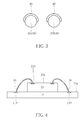
- FIG. 3 is a schematic, cross-sectional diagram showing the two adjacent bonding wires and the coated insulating material
- FIG. 4 to FIG. 7 are schematic, cross-sectional diagrams showing an exemplary method for forming the semiconductor package with coated bonding wires according to one embodiment of the invention
- FIG. 8 is a schematic top view of the semiconductor package showing an exemplary region around the semiconductor die, in which the insulating material is sprayed.
- FIG. 9 is a schematic, cross-sectional diagram showing a dipping process for coating an insulating material onto the bonding wires according to another embodiment of the invention.
- FIG. 1 is a schematic, cross-sectional diagram showing an exemplary semiconductor package with coated bonding wires according to one embodiment of the invention.
- FIG. 2 is a schematic, perspective view of two adjacent bonding wires in FIG. 1 without the molding compound for clarity.
- the semiconductor package 1 comprises a carrier substrate 10 having a top surface 10 a .
- a semiconductor die 20 is mounted on the top surface 10 a .
- the semiconductor die 20 has an active surface 20 a , on which a plurality of input/output (I/O) pads 210 is distributed.
- the semiconductor die 20 is electrically connected to the bond fingers 110 on the top surface 10 a of the carrier substrate 10 through a plurality of bonding wires 30 .
- the bonding wires 30 may comprise copper, gold, silver, or any suitable conductive materials.
- the carrier substrate 10 may comprise a packaging substrate, an interposer substrate, or a leadframe substrate, but is not limited thereto.
- the bonding wires 30 are partially coated with an insulating material 40 .
- the insulating material 40 may comprise polymers, epoxy, or resins, but is not limited thereto.
- the insulating material 40 coated on the bonding wires 30 may be cured to provide the bonding wires 30 with extra mechanical support.
- the insulating material 40 secures the bonding wires 30 and is able to resist the mold wire sweep during the encapsulation process of the semiconductor package 1 .
- the insulating material 40 has low permittivity or low dielectric constant (low-k) that can prevent shorting and alleviate crosstalk between adjacent wires.
- the bonding wires 30 may be fully coated with the insulating material 40 to provide a more desirable isolation effect.
- the semiconductor package 1 further comprises a molding compound 50 on the top surface 10 a of the carrier substrate 10 .
- the molding compound 50 encapsulates the bonding wires 30 , the insulating material 40 , and the semiconductor die 20 .
- the molding compound 50 may comprise an epoxy resin and a filler material, but is not limited thereto.
- the insulating material 40 may have the same epoxy composition as that of the molding compound 50 , but without the filler material or with lower content of the filler material.
- the insulating material 40 contains less than 50 ppm halogen content in order to prevent corrosion of the bonding wires 30 .
- the insulating material 40 may have a composition that is different from that of the molding compound 50 .
- the insulating material 40 is partially coated on the portions of the two adjacent bonding wires 30 a and 30 b that are most likely to short to the adjacent wires during the wire sweep that occurs during the encapsulation process of the semiconductor package 1 .
- the insulating material 40 may be also formed on the top surface 10 a of the carrier substrate 10 or elsewhere in the semiconductor package 1 .
- the insulating material 40 formed on the top surface 10 a of the carrier substrate 10 may enhance the interface adhesive strength between the molding compound 50 and the carrier substrate 10 .
- the two adjacent bonding wires 30 a and 30 b may have different loop heights. It is advantageous to use the present invention because the insulating material 40 coated on the bonding wires 30 a and 30 b can avoid abnormal wire sweep during encapsulation process and provide significant isolation effect. Furthermore, the loop heights of the two adjacent bonding wires 30 a and 30 b may be reduced such that more wires can be arranged in the same space.
- FIG. 3 is a schematic, cross-sectional diagram showing the two adjacent bonding wires and the coated insulating material.
- the insulating material 40 may only cover at least a partial portion, for example upper half portion, of each of the bonding wires 30 when viewed in cross-sections of the bonding wires 30 .
- the lower half portion of each of the bonding wires 30 is not covered by the insulating material 40 .
- each of the bonding wires 30 may be wrapped around by the insulating material 40 .
- FIG. 4 to FIG. 7 are schematic, cross-sectional diagrams showing an exemplary method for forming the semiconductor package with coated bonding wires according to one embodiment of the invention, wherein like numeral numbers designate like layers, regions, or elements.
- a semiconductor die 20 is mounted on a top surface 10 a of a carrier substrate 10 .
- the carrier substrate 10 may comprise a packaging substrate, an interposer substrate, or a leadframe substrate, but is not limited thereto.
- the semiconductor die 20 may be adhered to the top surface 10 a by using an adhesive (not explicitly shown), but is not limited thereto.
- the semiconductor die 20 is electrically connected to the bond fingers 110 on the top surface 10 a of the carrier substrate 10 through a plurality of bonding wires 30 .
- an insulating material 40 is sprayed onto the bonding wires 30 within predetermined regions.
- a region 140 is demonstrated around the semiconductor die 20 .
- the insulating material 40 may be sprayed onto the bonding wires 30 within the region 140 that would be most likely to short to the adjacent wires during the encapsulation process.
- the insulating material 40 may be sprayed onto the top surface 10 a of the carrier substrate 10 or onto the active surface 20 a of the semiconductor die 20 , which may enhance the interface adhesive strength between the molding compound and the substrate surface/die surface. It is understood the region 140 shown in FIG. 8 is for illustration purposes only.
- the insulating material 40 may be sprayed onto the bonding wires 30 by using a jet sprayer 400 or the like.
- the insulating material 40 may be coated onto the bonding wires 30 by using a dipping process.
- a container 500 contains the insulating material 40 in liquid phase.
- the package 1 is flipped and the bonding wires 30 may be partially dipped into the insulating material 40 to coat the bonding wires 30 .
- a drying process or baking process may be performed to remove the solvent.
- an optional curing process 600 may be carried out to cure the insulating material 40 .
- the curing process 600 may be carried out in an oven or under actinic radiation conditions, but is not limited thereto.
- the curing process 600 may be a fast curing process under ultraviolet (UV) or infrared (IR) irradiation. It is understood that the curing process 600 may be skipped in some embodiments, and the insulating material 40 may be cured at a later stage, together with the molding compound.
- UV ultraviolet
- IR infrared
- a molding compound 50 is formed on the top surface 10 a of the carrier substrate 10 to encapsulate the bonding wires 30 , the insulating material 40 , and the semiconductor die 20 .
- the molding compound 50 may comprise an epoxy resin and a filler material, but is not limited thereto.
- the insulating material 40 may have the same epoxy composition as that of the molding compound 50 , but without the filler material or with lower content of the filler material.
- the insulating material 40 contains less than 50 ppm halogen content in order to prevent corrosion of the bonding wires 30 .
Landscapes
- Structures Or Materials For Encapsulating Or Coating Semiconductor Devices Or Solid State Devices (AREA)
- Physics & Mathematics (AREA)
- Geometry (AREA)
- Wire Bonding (AREA)
- Encapsulation Of And Coatings For Semiconductor Or Solid State Devices (AREA)
Abstract
Description
Claims (9)
Priority Applications (6)
| Application Number | Priority Date | Filing Date | Title |
|---|---|---|---|
| US15/176,163 US10037936B2 (en) | 2015-11-02 | 2016-06-08 | Semiconductor package with coated bonding wires and fabrication method thereof |
| EP16177470.8A EP3163610A1 (en) | 2015-11-02 | 2016-07-01 | Semiconductor package with coated bonding wires |
| TW105129202A TW201717345A (en) | 2015-11-02 | 2016-09-09 | Semiconductor package and method of manufacturing same |
| CN201610834235.XA CN106941098A (en) | 2015-11-02 | 2016-09-20 | Semiconductor package and method of manufacturing the same |
| US15/894,874 US10847488B2 (en) | 2015-11-02 | 2018-02-12 | Semiconductor package having multi-tier bonding wires and components directly mounted on the multi-tier bonding wires |
| US16/836,665 US11257780B2 (en) | 2015-11-02 | 2020-03-31 | Semiconductor package having multi-tier bonding wires and components directly mounted on the multi-tier bonding wires |
Applications Claiming Priority (3)
| Application Number | Priority Date | Filing Date | Title |
|---|---|---|---|
| US201562249671P | 2015-11-02 | 2015-11-02 | |
| US201562251775P | 2015-11-06 | 2015-11-06 | |
| US15/176,163 US10037936B2 (en) | 2015-11-02 | 2016-06-08 | Semiconductor package with coated bonding wires and fabrication method thereof |
Related Child Applications (1)
| Application Number | Title | Priority Date | Filing Date |
|---|---|---|---|
| US15/894,874 Continuation-In-Part US10847488B2 (en) | 2015-11-02 | 2018-02-12 | Semiconductor package having multi-tier bonding wires and components directly mounted on the multi-tier bonding wires |
Publications (2)
| Publication Number | Publication Date |
|---|---|
| US20170125327A1 US20170125327A1 (en) | 2017-05-04 |
| US10037936B2 true US10037936B2 (en) | 2018-07-31 |
Family
ID=56296726
Family Applications (1)
| Application Number | Title | Priority Date | Filing Date |
|---|---|---|---|
| US15/176,163 Active US10037936B2 (en) | 2015-11-02 | 2016-06-08 | Semiconductor package with coated bonding wires and fabrication method thereof |
Country Status (4)
| Country | Link |
|---|---|
| US (1) | US10037936B2 (en) |
| EP (1) | EP3163610A1 (en) |
| CN (1) | CN106941098A (en) |
| TW (1) | TW201717345A (en) |
Cited By (1)
| Publication number | Priority date | Publication date | Assignee | Title |
|---|---|---|---|---|
| US10847488B2 (en) | 2015-11-02 | 2020-11-24 | Mediatek Inc. | Semiconductor package having multi-tier bonding wires and components directly mounted on the multi-tier bonding wires |
Families Citing this family (3)
| Publication number | Priority date | Publication date | Assignee | Title |
|---|---|---|---|---|
| US10217726B1 (en) | 2017-08-31 | 2019-02-26 | Micron Technology, Inc. | Stacked semiconductor dies including inductors and associated methods |
| US11264309B2 (en) * | 2019-06-24 | 2022-03-01 | Mediatek Inc. | Multi-row QFN semiconductor package |
| CN113013135A (en) * | 2021-02-09 | 2021-06-22 | 日月光半导体制造股份有限公司 | Routing, routing packaging structure, routing system and routing method |
Citations (12)
| Publication number | Priority date | Publication date | Assignee | Title |
|---|---|---|---|---|
| JP2000031195A (en) | 1998-07-16 | 2000-01-28 | Citizen Watch Co Ltd | Semiconductor device and method of manufacturing the same |
| US6531760B1 (en) * | 1988-09-20 | 2003-03-11 | Gen Murakami | Semiconductor device |
| DE102005025465A1 (en) | 2005-05-31 | 2006-12-14 | Infineon Technologies Ag | Semiconductor unit comprises a circuit carrier with interior contact areas, a semiconductor chip with an active surface and flipside and bonding wire connections between chip contact areas and interior contact areas of the circuit carrier |
| JP2006351737A (en) | 2005-06-15 | 2006-12-28 | Hitachi Ltd | Semiconductor power module |
| TW200712089A (en) | 2005-07-05 | 2007-04-01 | San Apro Ltd | Epoxy resin composition for sealing up optical semiconductor |
| US7202109B1 (en) * | 2004-11-17 | 2007-04-10 | National Semiconductor Corporation | Insulation and reinforcement of individual bonding wires in integrated circuit packages |
| WO2009079122A1 (en) | 2007-12-18 | 2009-06-25 | 3M Innovative Properties Company | Method of coating fine wires and curable composition therefor |
| US20100164083A1 (en) | 2008-12-29 | 2010-07-01 | Numonyx B.V. | Protective thin film coating in chip packaging |
| US20130175709A1 (en) * | 2012-01-10 | 2013-07-11 | Xilinx, Inc. | Integrated circuit package and method of assembling an integrated circuit package |
| JP2013197531A (en) | 2012-03-22 | 2013-09-30 | Sharp Corp | Semiconductor device and manufacturing method of the same |
| TW201443975A (en) | 2012-11-30 | 2014-11-16 | 山田尖端科技股份有限公司 | Photoresist film forming apparatus and method thereof, conductive film forming and circuit forming apparatus and method thereof, electromagnetic wave mask forming apparatus and method thereof, film forming apparatus for short-wavelength high transmittance insulating film, method thereof, and film formation of phosphor Device and method thereof, micro material synthesis device and method thereof, resin molding device, resin molding method, film forming device, organic EL element, bump forming device and method thereof, wiring forming device and method thereof, and wiring structure |
| TW201528450A (en) | 2013-11-29 | 2015-07-16 | 青井電子股份有限公司 | Semiconductor device and method of manufacturing the same |
Family Cites Families (5)
| Publication number | Priority date | Publication date | Assignee | Title |
|---|---|---|---|---|
| JPS61258436A (en) * | 1985-05-13 | 1986-11-15 | Nec Corp | Manufacture of semiconductor device |
| TWI249797B (en) * | 2004-12-06 | 2006-02-21 | Advanced Semiconductor Eng | Method for packaging a chip |
| KR20070030519A (en) * | 2005-09-13 | 2007-03-16 | 삼성전자주식회사 | Semiconductor package with bonding wire fixing means |
| KR20140055448A (en) * | 2012-10-31 | 2014-05-09 | 하나 마이크론(주) | Semiconductor package enabled to protect bonding wire |
| JP6164895B2 (en) * | 2013-04-02 | 2017-07-19 | ルネサスエレクトロニクス株式会社 | Manufacturing method of semiconductor device |
-
2016
- 2016-06-08 US US15/176,163 patent/US10037936B2/en active Active
- 2016-07-01 EP EP16177470.8A patent/EP3163610A1/en not_active Ceased
- 2016-09-09 TW TW105129202A patent/TW201717345A/en unknown
- 2016-09-20 CN CN201610834235.XA patent/CN106941098A/en not_active Withdrawn
Patent Citations (15)
| Publication number | Priority date | Publication date | Assignee | Title |
|---|---|---|---|---|
| US6531760B1 (en) * | 1988-09-20 | 2003-03-11 | Gen Murakami | Semiconductor device |
| JP2000031195A (en) | 1998-07-16 | 2000-01-28 | Citizen Watch Co Ltd | Semiconductor device and method of manufacturing the same |
| US7202109B1 (en) * | 2004-11-17 | 2007-04-10 | National Semiconductor Corporation | Insulation and reinforcement of individual bonding wires in integrated circuit packages |
| DE102005025465A1 (en) | 2005-05-31 | 2006-12-14 | Infineon Technologies Ag | Semiconductor unit comprises a circuit carrier with interior contact areas, a semiconductor chip with an active surface and flipside and bonding wire connections between chip contact areas and interior contact areas of the circuit carrier |
| US20070090539A1 (en) | 2005-05-31 | 2007-04-26 | Khalil Hosseini | Semiconductor device and method for producing the same |
| JP2006351737A (en) | 2005-06-15 | 2006-12-28 | Hitachi Ltd | Semiconductor power module |
| TW200712089A (en) | 2005-07-05 | 2007-04-01 | San Apro Ltd | Epoxy resin composition for sealing up optical semiconductor |
| WO2009079122A1 (en) | 2007-12-18 | 2009-06-25 | 3M Innovative Properties Company | Method of coating fine wires and curable composition therefor |
| US20100164083A1 (en) | 2008-12-29 | 2010-07-01 | Numonyx B.V. | Protective thin film coating in chip packaging |
| US20130175709A1 (en) * | 2012-01-10 | 2013-07-11 | Xilinx, Inc. | Integrated circuit package and method of assembling an integrated circuit package |
| JP2013197531A (en) | 2012-03-22 | 2013-09-30 | Sharp Corp | Semiconductor device and manufacturing method of the same |
| TW201443975A (en) | 2012-11-30 | 2014-11-16 | 山田尖端科技股份有限公司 | Photoresist film forming apparatus and method thereof, conductive film forming and circuit forming apparatus and method thereof, electromagnetic wave mask forming apparatus and method thereof, film forming apparatus for short-wavelength high transmittance insulating film, method thereof, and film formation of phosphor Device and method thereof, micro material synthesis device and method thereof, resin molding device, resin molding method, film forming device, organic EL element, bump forming device and method thereof, wiring forming device and method thereof, and wiring structure |
| US20150303151A1 (en) | 2012-11-30 | 2015-10-22 | Apic Yamada Corporation | Resist film forming device and method, conductive film forming and circuit forming device and method, electromagnetic wave shield forming device and method, shortwave high-transmissibility insulation film forming device and method, fluorescent light body film forming device and method, trace material combining device and method, resin molding device, resin molding method, thin film forming device, organic electroluminescence element, bump forming device and method, wiring forming device and method, and wiring structure body |
| TW201528450A (en) | 2013-11-29 | 2015-07-16 | 青井電子股份有限公司 | Semiconductor device and method of manufacturing the same |
| US20170053893A1 (en) | 2013-11-29 | 2017-02-23 | Aoi Electronics Co., Ltd. | Semiconductor Device and Method for Producing Semiconductor Device |
Non-Patent Citations (2)
| Title |
|---|
| PENG SU ; HIDETOSHI SEKI ; CHEN PING ; SHIN-ICHI ZENBUTSU ; SHINGO ITOH ; LOUIE HUANG ; NICHOLAS LIAO ; BILL LIU ; CURTIS CHEN ; W: "An evaluation of effects of molding compound properties on reliability of Cu wire components", ELECTRONIC COMPONENTS AND TECHNOLOGY CONFERENCE (ECTC), 2011 IEEE 61ST, IEEE, 31 May 2011 (2011-05-31), pages 363 - 369, XP031996564, ISBN: 978-1-61284-497-8, DOI: 10.1109/ECTC.2011.5898539 |
| Peng Su et al., An Evaluation of Effects of Molding Compound Properties on Reliability of Cu Wire Components, 2011 Electronic Components and Technology Conference, 2011, pp. 363-369, XP031996564, IEEE. |
Cited By (2)
| Publication number | Priority date | Publication date | Assignee | Title |
|---|---|---|---|---|
| US10847488B2 (en) | 2015-11-02 | 2020-11-24 | Mediatek Inc. | Semiconductor package having multi-tier bonding wires and components directly mounted on the multi-tier bonding wires |
| US11257780B2 (en) | 2015-11-02 | 2022-02-22 | Mediatek Inc. | Semiconductor package having multi-tier bonding wires and components directly mounted on the multi-tier bonding wires |
Also Published As
| Publication number | Publication date |
|---|---|
| TW201717345A (en) | 2017-05-16 |
| US20170125327A1 (en) | 2017-05-04 |
| EP3163610A1 (en) | 2017-05-03 |
| CN106941098A (en) | 2017-07-11 |
Similar Documents
| Publication | Publication Date | Title |
|---|---|---|
| US11257780B2 (en) | Semiconductor package having multi-tier bonding wires and components directly mounted on the multi-tier bonding wires | |
| TWI601247B (en) | Semiconductor package structure | |
| US20180076185A1 (en) | Method for fabricating a semiconductor package | |
| US6781222B2 (en) | Semiconductor package having vertically mounted passive devices under a chip and a fabricating method thereof | |
| US8420437B1 (en) | Method for forming an EMI shielding layer on all surfaces of a semiconductor package | |
| US5310702A (en) | Method of preventing short-circuiting of bonding wires | |
| US11810839B2 (en) | Semiconductor package with die stacked on surface mounted devices | |
| US20170125327A1 (en) | Semiconductor package with coated bonding wires and fabrication method thereof | |
| CN105977220B (en) | Semiconductor package assembly | |
| US11869849B2 (en) | Semiconductor package with EMI shielding structure | |
| US10685943B2 (en) | Semiconductor chip package with resilient conductive paste post and fabrication method thereof | |
| US11923319B2 (en) | Semiconductor package including sheilding cover that covers molded body | |
| KR100874925B1 (en) | Semiconductor package, manufacturing method thereof, card comprising same and system comprising same | |
| KR200489288Y1 (en) | Lead frame device and lead frame device assembly including the same | |
| EP3422404A1 (en) | Semiconductor package having multi-tier bonding wires and components directly mounted on the multi-tier bonding wires | |
| US9474162B2 (en) | Circuit substrate and method of manufacturing same | |
| JP2003124401A (en) | Module and manufacturing method thereof | |
| US7932131B2 (en) | Reduction of package height in a stacked die configuration | |
| JP2007534153A (en) | Semiconductor device packaging method including a plurality of elements, and semiconductor device | |
| US20160163629A1 (en) | Semiconductor package and method of fabricating the same | |
| KR20170016551A (en) | Semiconductor package | |
| JP2006032955A5 (en) | ||
| KR20150074786A (en) | Dispenser for coating Semiconductor Package and Method for Manufacturing Semiconductor Package using the same |
Legal Events
| Date | Code | Title | Description |
|---|---|---|---|
| AS | Assignment |
Owner name: MEDIATEK INC., TAIWAN Free format text: ASSIGNMENT OF ASSIGNORS INTEREST;ASSIGNORS:TSAI, SHIANN-TSONG;WANG, HSUEH-TE;CHANG, CHIN-CHIANG;REEL/FRAME:038837/0867 Effective date: 20160607 |
|
| STCF | Information on status: patent grant |
Free format text: PATENTED CASE |
|
| MAFP | Maintenance fee payment |
Free format text: PAYMENT OF MAINTENANCE FEE, 4TH YEAR, LARGE ENTITY (ORIGINAL EVENT CODE: M1551); ENTITY STATUS OF PATENT OWNER: LARGE ENTITY Year of fee payment: 4 |
|
| MAFP | Maintenance fee payment |
Free format text: PAYMENT OF MAINTENANCE FEE, 8TH YEAR, LARGE ENTITY (ORIGINAL EVENT CODE: M1552); ENTITY STATUS OF PATENT OWNER: LARGE ENTITY Year of fee payment: 8 |