US10014357B2 - Organic light-emitting device and organic light-emitting display device using the same - Google Patents
Organic light-emitting device and organic light-emitting display device using the same Download PDFInfo
- Publication number
- US10014357B2 US10014357B2 US15/718,158 US201715718158A US10014357B2 US 10014357 B2 US10014357 B2 US 10014357B2 US 201715718158 A US201715718158 A US 201715718158A US 10014357 B2 US10014357 B2 US 10014357B2
- Authority
- US
- United States
- Prior art keywords
- region
- charge generation
- generation layer
- type
- dopant
- Prior art date
- Legal status (The legal status is an assumption and is not a legal conclusion. Google has not performed a legal analysis and makes no representation as to the accuracy of the status listed.)
- Active
Links
- 239000002019 doping agent Substances 0.000 claims abstract description 199
- 239000011368 organic material Substances 0.000 claims abstract description 67
- 239000000758 substrate Substances 0.000 claims description 10
- 239000010409 thin film Substances 0.000 claims description 9
- 239000010410 layer Substances 0.000 description 365
- 238000004768 lowest unoccupied molecular orbital Methods 0.000 description 35
- 239000000463 material Substances 0.000 description 34
- 230000000052 comparative effect Effects 0.000 description 24
- 238000002347 injection Methods 0.000 description 15
- 239000007924 injection Substances 0.000 description 15
- 230000008859 change Effects 0.000 description 12
- 238000004770 highest occupied molecular orbital Methods 0.000 description 12
- 230000005525 hole transport Effects 0.000 description 12
- 230000004888 barrier function Effects 0.000 description 10
- 230000004048 modification Effects 0.000 description 9
- 238000012986 modification Methods 0.000 description 9
- 230000000694 effects Effects 0.000 description 8
- 235000019557 luminance Nutrition 0.000 description 7
- 230000005641 tunneling Effects 0.000 description 7
- 238000010586 diagram Methods 0.000 description 6
- 239000012044 organic layer Substances 0.000 description 6
- 239000004065 semiconductor Substances 0.000 description 6
- XFXPMWWXUTWYJX-UHFFFAOYSA-N Cyanide Chemical compound N#[C-] XFXPMWWXUTWYJX-UHFFFAOYSA-N 0.000 description 4
- -1 allyl compound Chemical class 0.000 description 4
- 125000003118 aryl group Chemical group 0.000 description 4
- 239000003086 colorant Substances 0.000 description 4
- 239000000470 constituent Substances 0.000 description 4
- 238000002474 experimental method Methods 0.000 description 4
- 239000010408 film Substances 0.000 description 4
- 150000002391 heterocyclic compounds Chemical class 0.000 description 4
- 238000000034 method Methods 0.000 description 4
- 229910052751 metal Inorganic materials 0.000 description 3
- 239000002184 metal Substances 0.000 description 3
- PXHVJJICTQNCMI-UHFFFAOYSA-N nickel Substances [Ni] PXHVJJICTQNCMI-UHFFFAOYSA-N 0.000 description 3
- 230000027756 respiratory electron transport chain Effects 0.000 description 3
- QENGPZGAWFQWCZ-UHFFFAOYSA-N 3-Methylthiophene Chemical compound CC=1C=CSC=1 QENGPZGAWFQWCZ-UHFFFAOYSA-N 0.000 description 2
- KRHYYFGTRYWZRS-UHFFFAOYSA-M Fluoride anion Chemical compound [F-] KRHYYFGTRYWZRS-UHFFFAOYSA-M 0.000 description 2
- KDLHZDBZIXYQEI-UHFFFAOYSA-N Palladium Chemical compound [Pd] KDLHZDBZIXYQEI-UHFFFAOYSA-N 0.000 description 2
- UFVXQDWNSAGPHN-UHFFFAOYSA-K bis[(2-methylquinolin-8-yl)oxy]-(4-phenylphenoxy)alumane Chemical compound [Al+3].C1=CC=C([O-])C2=NC(C)=CC=C21.C1=CC=C([O-])C2=NC(C)=CC=C21.C1=CC([O-])=CC=C1C1=CC=CC=C1 UFVXQDWNSAGPHN-UHFFFAOYSA-K 0.000 description 2
- 230000000903 blocking effect Effects 0.000 description 2
- 238000005401 electroluminescence Methods 0.000 description 2
- RAXXELZNTBOGNW-UHFFFAOYSA-N imidazole Natural products C1=CNC=N1 RAXXELZNTBOGNW-UHFFFAOYSA-N 0.000 description 2
- 229910010272 inorganic material Inorganic materials 0.000 description 2
- 239000011147 inorganic material Substances 0.000 description 2
- 229910044991 metal oxide Inorganic materials 0.000 description 2
- 150000004706 metal oxides Chemical class 0.000 description 2
- 150000002739 metals Chemical class 0.000 description 2
- 238000005424 photoluminescence Methods 0.000 description 2
- BASFCYQUMIYNBI-UHFFFAOYSA-N platinum Chemical compound [Pt] BASFCYQUMIYNBI-UHFFFAOYSA-N 0.000 description 2
- 229920000767 polyaniline Polymers 0.000 description 2
- 229920000128 polypyrrole Polymers 0.000 description 2
- 230000001681 protective effect Effects 0.000 description 2
- 238000001228 spectrum Methods 0.000 description 2
- 238000005011 time of flight secondary ion mass spectroscopy Methods 0.000 description 2
- 238000002042 time-of-flight secondary ion mass spectrometry Methods 0.000 description 2
- TVIVIEFSHFOWTE-UHFFFAOYSA-K tri(quinolin-8-yloxy)alumane Chemical compound [Al+3].C1=CN=C2C([O-])=CC=CC2=C1.C1=CN=C2C([O-])=CC=CC2=C1.C1=CN=C2C([O-])=CC=CC2=C1 TVIVIEFSHFOWTE-UHFFFAOYSA-K 0.000 description 2
- GEQBRULPNIVQPP-UHFFFAOYSA-N 2-[3,5-bis(1-phenylbenzimidazol-2-yl)phenyl]-1-phenylbenzimidazole Chemical compound C1=CC=CC=C1N1C2=CC=CC=C2N=C1C1=CC(C=2N(C3=CC=CC=C3N=2)C=2C=CC=CC=2)=CC(C=2N(C3=CC=CC=C3N=2)C=2C=CC=CC=2)=C1 GEQBRULPNIVQPP-UHFFFAOYSA-N 0.000 description 1
- BZXCOGNMFSSETH-UHFFFAOYSA-N 2-[4,5-bis(2-methoxyphenyl)-1,3-dimethyl-2-propan-2-ylimidazol-2-yl]-4,5-bis(3-methoxyphenyl)-1,3-dimethyl-2-propan-2-ylimidazole Chemical compound COC1=CC=CC(C=2N(C(C(C)C)(N(C)C=2C=2C=C(OC)C=CC=2)C2(C(C)C)N(C(=C(N2C)C=2C(=CC=CC=2)OC)C=2C(=CC=CC=2)OC)C)C)=C1 BZXCOGNMFSSETH-UHFFFAOYSA-N 0.000 description 1
- AOUOXXCMWHQDIH-UHFFFAOYSA-N 2-[4,5-bis(2-methoxyphenyl)-1,3-dimethyl-2-propan-2-ylimidazol-2-yl]-4,5-bis(4-methoxyphenyl)-1,3-dimethyl-2-propan-2-ylimidazole Chemical compound C1=CC(OC)=CC=C1C1=C(C=2C=CC(OC)=CC=2)N(C)C(C(C)C)(C2(C(C)C)N(C(=C(N2C)C=2C(=CC=CC=2)OC)C=2C(=CC=CC=2)OC)C)N1C AOUOXXCMWHQDIH-UHFFFAOYSA-N 0.000 description 1
- WMAXWOOEPJQXEB-UHFFFAOYSA-N 2-phenyl-5-(4-phenylphenyl)-1,3,4-oxadiazole Chemical compound C1=CC=CC=C1C1=NN=C(C=2C=CC(=CC=2)C=2C=CC=CC=2)O1 WMAXWOOEPJQXEB-UHFFFAOYSA-N 0.000 description 1
- ZVFQEOPUXVPSLB-UHFFFAOYSA-N 3-(4-tert-butylphenyl)-4-phenyl-5-(4-phenylphenyl)-1,2,4-triazole Chemical compound C1=CC(C(C)(C)C)=CC=C1C(N1C=2C=CC=CC=2)=NN=C1C1=CC=C(C=2C=CC=CC=2)C=C1 ZVFQEOPUXVPSLB-UHFFFAOYSA-N 0.000 description 1
- 101500028161 Homo sapiens Tumor necrosis factor-binding protein 1 Proteins 0.000 description 1
- 229920000292 Polyquinoline Polymers 0.000 description 1
- NRCMAYZCPIVABH-UHFFFAOYSA-N Quinacridone Chemical class N1C2=CC=CC=C2C(=O)C2=C1C=C1C(=O)C3=CC=CC=C3NC1=C2 NRCMAYZCPIVABH-UHFFFAOYSA-N 0.000 description 1
- BQCADISMDOOEFD-UHFFFAOYSA-N Silver Chemical compound [Ag] BQCADISMDOOEFD-UHFFFAOYSA-N 0.000 description 1
- 102400000089 Tumor necrosis factor-binding protein 1 Human genes 0.000 description 1
- 229910052783 alkali metal Inorganic materials 0.000 description 1
- 150000001340 alkali metals Chemical class 0.000 description 1
- 229910052784 alkaline earth metal Inorganic materials 0.000 description 1
- 229910052782 aluminium Inorganic materials 0.000 description 1
- XAGFODPZIPBFFR-UHFFFAOYSA-N aluminium Chemical compound [Al] XAGFODPZIPBFFR-UHFFFAOYSA-N 0.000 description 1
- 229910021417 amorphous silicon Inorganic materials 0.000 description 1
- MWPLVEDNUUSJAV-UHFFFAOYSA-N anthracene Chemical class C1=CC=CC2=CC3=CC=CC=C3C=C21 MWPLVEDNUUSJAV-UHFFFAOYSA-N 0.000 description 1
- 150000004982 aromatic amines Chemical class 0.000 description 1
- HRQXKKFGTIWTCA-UHFFFAOYSA-L beryllium;2-pyridin-2-ylphenolate Chemical compound [Be+2].[O-]C1=CC=CC=C1C1=CC=CC=N1.[O-]C1=CC=CC=C1C1=CC=CC=N1 HRQXKKFGTIWTCA-UHFFFAOYSA-L 0.000 description 1
- 239000006229 carbon black Substances 0.000 description 1
- 239000012876 carrier material Substances 0.000 description 1
- 230000002860 competitive effect Effects 0.000 description 1
- 230000000295 complement effect Effects 0.000 description 1
- 150000001875 compounds Chemical class 0.000 description 1
- 229920001940 conductive polymer Polymers 0.000 description 1
- 150000004696 coordination complex Chemical class 0.000 description 1
- 239000010949 copper Substances 0.000 description 1
- GBRBMTNGQBKBQE-UHFFFAOYSA-L copper;diiodide Chemical compound I[Cu]I GBRBMTNGQBKBQE-UHFFFAOYSA-L 0.000 description 1
- 238000002484 cyclic voltammetry Methods 0.000 description 1
- 230000003247 decreasing effect Effects 0.000 description 1
- 238000013461 design Methods 0.000 description 1
- CZZYITDELCSZES-UHFFFAOYSA-N diphenylmethane Chemical class C=1C=CC=CC=1CC1=CC=CC=C1 CZZYITDELCSZES-UHFFFAOYSA-N 0.000 description 1
- 230000008020 evaporation Effects 0.000 description 1
- 238000001704 evaporation Methods 0.000 description 1
- 230000005281 excited state Effects 0.000 description 1
- KTWOOEGAPBSYNW-UHFFFAOYSA-N ferrocene Chemical compound [Fe+2].C=1C=C[CH-]C=1.C=1C=C[CH-]C=1 KTWOOEGAPBSYNW-UHFFFAOYSA-N 0.000 description 1
- 125000003983 fluorenyl group Chemical group C1(=CC=CC=2C3=CC=CC=C3CC12)* 0.000 description 1
- PCHJSUWPFVWCPO-UHFFFAOYSA-N gold Chemical compound [Au] PCHJSUWPFVWCPO-UHFFFAOYSA-N 0.000 description 1
- 229910052737 gold Inorganic materials 0.000 description 1
- 239000010931 gold Substances 0.000 description 1
- 230000005283 ground state Effects 0.000 description 1
- 150000002429 hydrazines Chemical class 0.000 description 1
- 150000002460 imidazoles Chemical class 0.000 description 1
- 230000006872 improvement Effects 0.000 description 1
- APFVFJFRJDLVQX-UHFFFAOYSA-N indium atom Chemical compound [In] APFVFJFRJDLVQX-UHFFFAOYSA-N 0.000 description 1
- 229910003437 indium oxide Inorganic materials 0.000 description 1
- 239000004973 liquid crystal related substance Substances 0.000 description 1
- 238000004519 manufacturing process Methods 0.000 description 1
- 239000011159 matrix material Substances 0.000 description 1
- 239000000203 mixture Substances 0.000 description 1
- 229910052759 nickel Inorganic materials 0.000 description 1
- 230000003287 optical effect Effects 0.000 description 1
- 150000004866 oxadiazoles Chemical class 0.000 description 1
- 230000003647 oxidation Effects 0.000 description 1
- 238000007254 oxidation reaction Methods 0.000 description 1
- 229910052763 palladium Inorganic materials 0.000 description 1
- IEQIEDJGQAUEQZ-UHFFFAOYSA-N phthalocyanine Chemical class N1C(N=C2C3=CC=CC=C3C(N=C3C4=CC=CC=C4C(=N4)N3)=N2)=C(C=CC=C2)C2=C1N=C1C2=CC=CC=C2C4=N1 IEQIEDJGQAUEQZ-UHFFFAOYSA-N 0.000 description 1
- 230000000704 physical effect Effects 0.000 description 1
- 229910052697 platinum Inorganic materials 0.000 description 1
- 229920000553 poly(phenylenevinylene) Polymers 0.000 description 1
- 229910021420 polycrystalline silicon Inorganic materials 0.000 description 1
- 229920005591 polysilicon Polymers 0.000 description 1
- 229920000123 polythiophene Polymers 0.000 description 1
- 150000004033 porphyrin derivatives Chemical class 0.000 description 1
- 230000008569 process Effects 0.000 description 1
- 238000012545 processing Methods 0.000 description 1
- 230000009467 reduction Effects 0.000 description 1
- 238000002310 reflectometry Methods 0.000 description 1
- FZHAPNGMFPVSLP-UHFFFAOYSA-N silanamine Chemical class [SiH3]N FZHAPNGMFPVSLP-UHFFFAOYSA-N 0.000 description 1
- 229910052709 silver Inorganic materials 0.000 description 1
- 239000004332 silver Substances 0.000 description 1
- 230000003595 spectral effect Effects 0.000 description 1
- PFBLRDXPNUJYJM-UHFFFAOYSA-N tert-butyl 2-methylpropaneperoxoate Chemical compound CC(C)C(=O)OOC(C)(C)C PFBLRDXPNUJYJM-UHFFFAOYSA-N 0.000 description 1
- 150000003512 tertiary amines Chemical class 0.000 description 1
- 229910001887 tin oxide Inorganic materials 0.000 description 1
- QHGNHLZPVBIIPX-UHFFFAOYSA-N tin(ii) oxide Chemical class [Sn]=O QHGNHLZPVBIIPX-UHFFFAOYSA-N 0.000 description 1
- 238000012546 transfer Methods 0.000 description 1
- 238000007740 vapor deposition Methods 0.000 description 1
Images


Classifications
-
- H—ELECTRICITY
- H10—SEMICONDUCTOR DEVICES; ELECTRIC SOLID-STATE DEVICES NOT OTHERWISE PROVIDED FOR
- H10K—ORGANIC ELECTRIC SOLID-STATE DEVICES
- H10K50/00—Organic light-emitting devices
- H10K50/10—OLEDs or polymer light-emitting diodes [PLED]
- H10K50/11—OLEDs or polymer light-emitting diodes [PLED] characterised by the electroluminescent [EL] layers
- H10K50/125—OLEDs or polymer light-emitting diodes [PLED] characterised by the electroluminescent [EL] layers specially adapted for multicolour light emission, e.g. for emitting white light
- H10K50/13—OLEDs or polymer light-emitting diodes [PLED] characterised by the electroluminescent [EL] layers specially adapted for multicolour light emission, e.g. for emitting white light comprising stacked EL layers within one EL unit
- H10K50/131—OLEDs or polymer light-emitting diodes [PLED] characterised by the electroluminescent [EL] layers specially adapted for multicolour light emission, e.g. for emitting white light comprising stacked EL layers within one EL unit with spacer layers between the electroluminescent layers
-
- H—ELECTRICITY
- H10—SEMICONDUCTOR DEVICES; ELECTRIC SOLID-STATE DEVICES NOT OTHERWISE PROVIDED FOR
- H10K—ORGANIC ELECTRIC SOLID-STATE DEVICES
- H10K59/00—Integrated devices, or assemblies of multiple devices, comprising at least one organic light-emitting element covered by group H10K50/00
- H10K59/10—OLED displays
- H10K59/12—Active-matrix OLED [AMOLED] displays
- H10K59/123—Connection of the pixel electrodes to the thin film transistors [TFT]
-
- H01L27/3248—
-
- H01L27/322—
-
- H01L51/5004—
-
- H01L51/5203—
-
- H—ELECTRICITY
- H10—SEMICONDUCTOR DEVICES; ELECTRIC SOLID-STATE DEVICES NOT OTHERWISE PROVIDED FOR
- H10K—ORGANIC ELECTRIC SOLID-STATE DEVICES
- H10K50/00—Organic light-emitting devices
- H10K50/10—OLEDs or polymer light-emitting diodes [PLED]
- H10K50/11—OLEDs or polymer light-emitting diodes [PLED] characterised by the electroluminescent [EL] layers
-
- H—ELECTRICITY
- H10—SEMICONDUCTOR DEVICES; ELECTRIC SOLID-STATE DEVICES NOT OTHERWISE PROVIDED FOR
- H10K—ORGANIC ELECTRIC SOLID-STATE DEVICES
- H10K50/00—Organic light-emitting devices
- H10K50/10—OLEDs or polymer light-emitting diodes [PLED]
- H10K50/17—Carrier injection layers
-
- H—ELECTRICITY
- H10—SEMICONDUCTOR DEVICES; ELECTRIC SOLID-STATE DEVICES NOT OTHERWISE PROVIDED FOR
- H10K—ORGANIC ELECTRIC SOLID-STATE DEVICES
- H10K50/00—Organic light-emitting devices
- H10K50/10—OLEDs or polymer light-emitting diodes [PLED]
- H10K50/17—Carrier injection layers
- H10K50/171—Electron injection layers
-
- H—ELECTRICITY
- H10—SEMICONDUCTOR DEVICES; ELECTRIC SOLID-STATE DEVICES NOT OTHERWISE PROVIDED FOR
- H10K—ORGANIC ELECTRIC SOLID-STATE DEVICES
- H10K50/00—Organic light-emitting devices
- H10K50/10—OLEDs or polymer light-emitting diodes [PLED]
- H10K50/19—Tandem OLEDs
-
- H—ELECTRICITY
- H10—SEMICONDUCTOR DEVICES; ELECTRIC SOLID-STATE DEVICES NOT OTHERWISE PROVIDED FOR
- H10K—ORGANIC ELECTRIC SOLID-STATE DEVICES
- H10K50/00—Organic light-emitting devices
- H10K50/80—Constructional details
- H10K50/805—Electrodes
-
- H—ELECTRICITY
- H10—SEMICONDUCTOR DEVICES; ELECTRIC SOLID-STATE DEVICES NOT OTHERWISE PROVIDED FOR
- H10K—ORGANIC ELECTRIC SOLID-STATE DEVICES
- H10K59/00—Integrated devices, or assemblies of multiple devices, comprising at least one organic light-emitting element covered by group H10K50/00
- H10K59/10—OLED displays
- H10K59/12—Active-matrix OLED [AMOLED] displays
- H10K59/121—Active-matrix OLED [AMOLED] displays characterised by the geometry or disposition of pixel elements
- H10K59/1213—Active-matrix OLED [AMOLED] displays characterised by the geometry or disposition of pixel elements the pixel elements being TFTs
-
- H—ELECTRICITY
- H10—SEMICONDUCTOR DEVICES; ELECTRIC SOLID-STATE DEVICES NOT OTHERWISE PROVIDED FOR
- H10K—ORGANIC ELECTRIC SOLID-STATE DEVICES
- H10K59/00—Integrated devices, or assemblies of multiple devices, comprising at least one organic light-emitting element covered by group H10K50/00
- H10K59/30—Devices specially adapted for multicolour light emission
- H10K59/32—Stacked devices having two or more layers, each emitting at different wavelengths
-
- H—ELECTRICITY
- H10—SEMICONDUCTOR DEVICES; ELECTRIC SOLID-STATE DEVICES NOT OTHERWISE PROVIDED FOR
- H10K—ORGANIC ELECTRIC SOLID-STATE DEVICES
- H10K59/00—Integrated devices, or assemblies of multiple devices, comprising at least one organic light-emitting element covered by group H10K50/00
- H10K59/30—Devices specially adapted for multicolour light emission
- H10K59/35—Devices specially adapted for multicolour light emission comprising red-green-blue [RGB] subpixels
-
- H—ELECTRICITY
- H10—SEMICONDUCTOR DEVICES; ELECTRIC SOLID-STATE DEVICES NOT OTHERWISE PROVIDED FOR
- H10K—ORGANIC ELECTRIC SOLID-STATE DEVICES
- H10K59/00—Integrated devices, or assemblies of multiple devices, comprising at least one organic light-emitting element covered by group H10K50/00
- H10K59/30—Devices specially adapted for multicolour light emission
- H10K59/38—Devices specially adapted for multicolour light emission comprising colour filters or colour changing media [CCM]
-
- H—ELECTRICITY
- H10—SEMICONDUCTOR DEVICES; ELECTRIC SOLID-STATE DEVICES NOT OTHERWISE PROVIDED FOR
- H10K—ORGANIC ELECTRIC SOLID-STATE DEVICES
- H10K59/00—Integrated devices, or assemblies of multiple devices, comprising at least one organic light-emitting element covered by group H10K50/00
- H10K59/80—Constructional details
- H10K59/805—Electrodes
-
- H—ELECTRICITY
- H10—SEMICONDUCTOR DEVICES; ELECTRIC SOLID-STATE DEVICES NOT OTHERWISE PROVIDED FOR
- H10K—ORGANIC ELECTRIC SOLID-STATE DEVICES
- H10K71/00—Manufacture or treatment specially adapted for the organic devices covered by this subclass
- H10K71/30—Doping active layers, e.g. electron transporting layers
-
- H01L27/3246—
-
- H01L51/5056—
-
- H01L51/5072—
-
- H—ELECTRICITY
- H10—SEMICONDUCTOR DEVICES; ELECTRIC SOLID-STATE DEVICES NOT OTHERWISE PROVIDED FOR
- H10K—ORGANIC ELECTRIC SOLID-STATE DEVICES
- H10K2101/00—Properties of the organic materials covered by group H10K85/00
- H10K2101/40—Interrelation of parameters between multiple constituent active layers or sublayers, e.g. HOMO values in adjacent layers
-
- H—ELECTRICITY
- H10—SEMICONDUCTOR DEVICES; ELECTRIC SOLID-STATE DEVICES NOT OTHERWISE PROVIDED FOR
- H10K—ORGANIC ELECTRIC SOLID-STATE DEVICES
- H10K2101/00—Properties of the organic materials covered by group H10K85/00
- H10K2101/80—Composition varying spatially, e.g. having a spatial gradient
-
- H—ELECTRICITY
- H10—SEMICONDUCTOR DEVICES; ELECTRIC SOLID-STATE DEVICES NOT OTHERWISE PROVIDED FOR
- H10K—ORGANIC ELECTRIC SOLID-STATE DEVICES
- H10K2102/00—Constructional details relating to the organic devices covered by this subclass
- H10K2102/301—Details of OLEDs
- H10K2102/351—Thickness
-
- H—ELECTRICITY
- H10—SEMICONDUCTOR DEVICES; ELECTRIC SOLID-STATE DEVICES NOT OTHERWISE PROVIDED FOR
- H10K—ORGANIC ELECTRIC SOLID-STATE DEVICES
- H10K50/00—Organic light-emitting devices
- H10K50/10—OLEDs or polymer light-emitting diodes [PLED]
- H10K50/14—Carrier transporting layers
- H10K50/15—Hole transporting layers
-
- H—ELECTRICITY
- H10—SEMICONDUCTOR DEVICES; ELECTRIC SOLID-STATE DEVICES NOT OTHERWISE PROVIDED FOR
- H10K—ORGANIC ELECTRIC SOLID-STATE DEVICES
- H10K50/00—Organic light-emitting devices
- H10K50/10—OLEDs or polymer light-emitting diodes [PLED]
- H10K50/14—Carrier transporting layers
- H10K50/16—Electron transporting layers
-
- H—ELECTRICITY
- H10—SEMICONDUCTOR DEVICES; ELECTRIC SOLID-STATE DEVICES NOT OTHERWISE PROVIDED FOR
- H10K—ORGANIC ELECTRIC SOLID-STATE DEVICES
- H10K59/00—Integrated devices, or assemblies of multiple devices, comprising at least one organic light-emitting element covered by group H10K50/00
- H10K59/10—OLED displays
- H10K59/12—Active-matrix OLED [AMOLED] displays
- H10K59/122—Pixel-defining structures or layers, e.g. banks
Definitions
- the present disclosure relates to an organic light-emitting device, and more particularly, to an organic light-emitting device that provides a charge generation layer between a plurality stacks and an organic light-emitting display device using the same.
- LCDs liquid crystal displays
- PDPs plasma display panels
- FEDs field emission displays
- OLED organic light-emitting device
- the organic light-emitting display includes a plurality of sub-pixels, and each sub-pixel includes an organic light-emitting device (OLED).
- OLED organic light-emitting device
- the term “OLED” may also be used to refer to an “organic light-emitting diode.”
- OLEDs are independently driven on a sub-pixel basis, including an anode and a cathode, and a plurality of organic layers between the anode and the cathode.
- the organic light-emitting device is used for a lighting and a display, including a flexible display device and a transparent display device, because the organic light-emitting device does not require an additional light source.
- At least one layer of the organic layers between the anode and the cathode is an organic light-emitting layer. Holes and electrons from the anode and cathode are injected into the organic light-emitting layer, and are combined with each other in the organic light-emitting layer, thus generating excitons. When the generated excitons are changed from an excited state to a ground state, the organic light-emitting diode emits light.
- tandem-type organic light-emitting device having a plurality of stacks between an anode and a cathode and a charge generation layer between two stacks, has been introduced to improve efficiency of an organic light-emitting device having a single stack between an anode and a cathode.
- tandem-type organic light-emitting device transportability of electrons is relatively slower than transportability of holes in an emitting layer of the stack, which is far from the cathode.
- transportability of electrons is relatively slower than transportability of holes in an emitting layer of the stack, which is far from the cathode.
- an emission efficiency is lowered and differences of transportability between holes and electrons in the emitting layers becomes greater as time passes. Therefore, a balance between holes and electrons in the emitting layer collapses, and then, it is difficult to have a long lifespan of the device.
- the present disclosure is directed to an organic light-emitting device and an organic light-emitting display device using the same that substantially obviate one or more of the issues due to limitations and disadvantages of the related art.
- embodiments of the present disclosure may provide an organic light-emitting device that provides a charge generation layer between a plurality stacks, including an n-type dopant whose content is changed within the charge generation layer to increase transportability of electrons, and an organic light-emitting display device using the same.
- an organic light-emitting device including: an anode and a cathode opposite each other, a first stack and a second stack between the anode and the cathode, and a charge generation layer between the first stack and the second stack, the charge generation layer including an n-type charge generation layer and a p-type charge generation layer, wherein the p-type charge generation layer includes one first organic material, wherein the n-type charge generation layer includes a second organic material and an n-type dopant, wherein the n-type charge generation layer is divided into a first region contacting the first stack, a second region contacting the p-type charge generation layer, and a third region between the first region and the second region, and wherein a dopant content of the n-type dopant is stepwise increased in an order of: the first region, the third region, and the second region.
- an organic light-emitting device including: an anode and a cathode opposing each other, a first stack and a second stack between the anode and the cathode, and a charge generation layer between the first stack and the second stack, the charge generation layer including an n-type charge generation layer and a p-type charge generation layer, wherein the p-type charge generation layer includes one first organic material, wherein the n-type charge generation layer includes a second organic material and an n type dopant, wherein the n-type charge generation layer is divided into a first region contacting the first stack, a second region contacting the p-type charge generation layer, and a third region between the first region and the second region, wherein the n-type dopant is only in the second region and the third region, and wherein a dopant content of the n-type dopant in the second region is greatest within the n-type charge generation layer.
- an organic light-emitting display device including: a substrate including a plurality of subpixels, a thin-film transistor in each subpixel on the substrate, and an organic light-emitting device at each sub-pixel, the organic light-emitting device including: an anode and a cathode opposing each other, a first stack and a second stack between the anode and the cathode, and a charge generation layer between the first stack and the second stack, wherein the thin-film transistor contacts the anode or the cathode, wherein the charge generation layer includes: an n-type charge generation layer, and a p-type charge generation layer, wherein the p-type charge generation layer includes one first organic material, wherein the n-type charge generation layer includes a second organic material and an n-type dopant, wherein the n-type charge generation layer is divided into a first region contacting the first stack, a second region contacting the p-type charge generation layer, and a third region
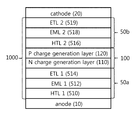
- FIG. 1 is a cross-sectional view illustrating an organic light-emitting device in accordance with a first example embodiment of the present disclosure.
- FIG. 2 shows a structure and content of the n-type charge generation layer in FIG. 1 .
- FIG. 3A is a band diagram for a charge generation layer and other layers adjacent to the charge generation layer in accordance with a first comparative example.
- FIG. 3B is a graph illustrating a change of an energy band for a charge generation layer and other layers adjacent to the charge generation layer when a current is applied in accordance with a first comparative example.
- FIG. 4A is a band diagram for a charge generation layer and other layers adjacent to the charge generation layer in accordance with an example embodiment of the present disclosure.
- FIG. 4B is a graph illustrating a change of an energy band for a charge generation layer and other layers adjacent to the charge generation layer when a current is applied in accordance with an experimental example.
- FIG. 5 is an enlarged view illustrating the change of the energy band between the n-type charge generation layer and the p-type charge generation layer in FIG. 4B .
- FIG. 6 is a graph showing content of the n-type charge generation layer in accordance with a modification of the first example embodiment of the present disclosure.
- FIG. 7 is a graph showing content of the n-type charge generation layer in accordance with a different modification of the first example embodiment of the present disclosure.
- FIG. 8 is a cross-sectional view illustrating an organic light-emitting device in accordance with a second example embodiment of the present disclosure.
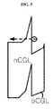
- FIGS. 9A-9D are energy diagrams showing the charge generation layer and adjacent layers to the charge generation layer in accordance with example embodiments of the present disclosure.
- FIG. 10 is a graph illustrating luminance in accordance with a second comparative example and the examples of FIGS. 9A-9D .
- FIG. 11 is a graph illustrating a change in voltage ( ⁇ V) in accordance with the second comparative example and the examples of FIGS. 9A-9D .
- FIG. 12 is a cross-sectional view illustrating an organic light-emitting display device in accordance with an example embodiment of the present disclosure.
- the “lowest unoccupied molecular orbital (LUMO) energy level” and the “highest occupied molecular orbital (HOMO) energy level” of any layer indicate the LUMO energy level and the HOMO energy level of a material that occupies the greatest weight percentage of the corresponding layer, for example, a host material, and do not refer to the LUMO energy level and the HOMO energy level of a dopant material doped on the corresponding layer unless otherwise mentioned.
- the “HOMO energy level” may be the energy level measured by cyclic voltammetry (CV) that determines the energy level from a potential value relative to a reference electrode, the potential value of which is known.
- CV cyclic voltammetry
- the HOMO energy level of any material may be measured using ferrocene, the oxidation potential value and the reduction potential value of which are known, as a reference electrode.
- the term “doped” indicates that the material that occupies the greatest weight percentage of any layer is added with a material that has a different physical property (for example, an N-type or P-type or an organic material or an inorganic material) from that of the material that occupies the greatest weight percentage in an amount corresponding to a weight percentage less than 10%.
- a “doped” layer indicates a layer, the host material and the dopant material of which may be distinguished from each other based on the weight percentages thereof.
- the term “undoped” refers to all cases excluding the case corresponding to the term “doped.”
- the layer belongs to the “undoped” layer.
- the layer belongs to the “undoped” layer.
- the layer belongs to the “undoped” layer.
- the layer belongs to the “undoped” layer.
- the layer belongs to the “undoped” layer.
- any layer is mainly formed of organic materials
- at least one material of the layer is of an N-type and at least one other material of the layer is of a P-type
- the layer belongs to the “doped” layer when the weight percentage of the N-type material is less than 10% or the weight percentage of the P-type material is less than 10%.
- an electroluminescence (EL) spectrum is calculated by multiplying (1) a photoluminescence (PL) spectrum that reflects the unique properties of a luminescent material, such as a dopant material or a host material included in an organic light-emitting layer, by (2) an outcoupling spectral emittance curve that is determined based on the structure of an organic light-emitting element including the thicknesses of organic layers such as, for example, an electron transport layer, and optical properties thereof.
- PL photoluminescence
- the term “stack” refers to a unit structure that includes organic layers such as a hole transport layer and an electron transport layer and an organic light-emitting layer interposed between the hole transport layer and the electron transport layer.
- the organic layers may further include a hole injection layer, an electron blocking layer, a hole blocking layer, and an electron injection layer, and may further include other organic layers according to the structure or design of the organic light-emitting element.
- FIG. 1 is a cross-sectional view illustrating an organic light-emitting device in accordance with a first example embodiment of the present disclosure.
- FIG. 2 shows a structure and content of the n-type charge generation layer in FIG. 1 .
- an organic light-emitting device may include an anode 10 and a cathode 20 facing each other, a first stack 50 a and a second stack 50 b between the anode 10 and the cathode 20 , and a charge generation layer 100 between the first stack 50 a and the second stack 50 b .
- the charge generation layer 100 may include an n-type charge generation layer 110 and a p-type charge generation layer 120 .
- the charge generation layer 100 may consist of the n-type charge generation layer 110 and the p-type charge generation layer 120 .
- the p-type charge generation layer 120 may include one first organic material, and the n-type charge generation layer 110 may include a second organic material and an n-type dopant. Also, the p-type charge generation layer 120 may consist of the one first organic material.
- the n-type charge generation layer 110 may be divided into a first region 110 a contacting the first stack 50 a , a second region 100 c contacting the p-type charge generation layer 120 , and a third region 110 b between the first region 110 a and the second region 110 c .
- a content of the n-type dopant according to the first embodiment of the organic light-emitting device may exist in the third region 110 b and the second region 110 c , and the dopant content of the n-type dopant may be highest in the second region 110 c of the n-type charge generation layer 110 .
- the charge generation layer (CGL) 100 may be referred to as an “intermediate connector layer” because the charge generation layer 100 may control a balance of holes and electrons between the first stack 50 a and the second stack 50 b .
- the n-type charge generation layer 110 may help an injection of electrons into the first stack 50 a
- the p-type charge generation layer 120 may help an injection of holes into the second stack 50 b.
- the p-type charge generation layer 120 may include a single first organic material.
- the single first organic material may be the same as a material of a second hole transport layer (HTL2) 516 in the second stack 50 b .
- the single first organic material of the p-type charge generation layer 120 may be any one among a fused aromatic group of a heterocyclic compound having at least one of Cyanide (CN) and Fluoride (F), or an allyl compound.
- the p-type charge generation layer 120 may consist of the single first organic material.
- the second organic material included in the n-type charge generation layer 110 may be an organic material having electron transportability.
- the second organic material may include a fused aromatic group of a heterocyclic compound.
- the second organic material may be an oxadiazole derivative, an antracene derivative, or may be one of: Alq 3 , PBD, TAZ, Spiro-PBD, BAlq, SAlq, PF-6P, BMB-3T, CO, and TBPI.
- the n-type dopant included in the n-type charge generation layer 110 may be an alkali metal or an alkali earth metal or an n-type organic dopant.
- the n-type organic dopant may be any one of: Cr2hpp 4 (hpp: 1,3,4,6,7,8-hexahydro-2H-pyrimido[1,2-a]pyrimidine anion), Fe 2 hpp 4 , Mn 2 hpp 4 , Co 2 hpp 4 , Mo 2 hpp 4 , W 2 hpp 4 , Ni 2 hpp 4 , Cu 2 hpp 4 , Zn 2 hpp 4 , W(hpp) 4 , 4,4′,5,5′-tetracyclohexyl-1,1′,2,2′,3,3′-hexamethyl-2,2′,3,3-tetrahydro-1H,1′H-2,2′-biimidazole or 2,2′-diisopropy
- the dopant content of the n-dopant may be stepwise ratcheted up in an order of: the first region 110 a , the third region 110 b , and the second region 110 c . That is, the n-type charge generation layer 110 may be divided into a plurality of regions having different contents of the n-type dopant. In each region, a same content may remain.
- the organic light-emitting device may include the first region 110 a having no n-type dopant.
- the first region 110 a may contact the first stack 50 a . That is, the second organic material may be provided only for a certain thickness to form the first region 110 a , and then n-dopant may be further provided with the second organic material to form the third region 110 b and the second region 110 c by applying different contents of the n-type dopant to increase contents of the n-dopant when forming the n-type charge generation layer 110 .
- the dopant content of the n-type dopant may be stepwise ratcheted up in an order of: the first region 110 a , the third region 110 b , and the second region 110 c.
- the dopant content “d1” of the n-type dopant between the first region 110 a and the third region 110 b may be smaller than the dopant content difference “d2 ⁇ d1” of the n-type dopant between the third region 110 b and the second region 110 c so that the n-type dopant in the n-type charge generation layer 110 may be relatively concentrated at an interface of the n-type charge generation layer 110 and the p-type charge generation layer 120 .
- the electrons from the p-type charge generation layer 120 may quickly enter the n-type charge generation layer 110 by causing a quantum tunneling effect through a sharp change of a conduction band energy at an interface between the p-type charge generation layer 120 and the n-type charge generation layer 110 .
- the n-type dopant may be locally concentrated at the second region 110 c , which may contact the p-type charge generation layer 120 , which may provide a short tunnel in which the electrons may pass, regardless of an energy barrier in the second region 110 c .
- the p-type charge generation layer 120 may include a single first organic material
- HOMO and LUMO energies may be respectively maintained in the p-type charge generation layer 120 .
- the HOMO and LUMO energies of the second organic material included in the n-type charge generation layer 110 may be pre-determined according to the material of the second organic material.
- the second organic material may be a main material in the n-type organic generation layer 110 to help to generate electrons and transport electrons.
- the HOMO and LUMO energies of the second organic material may be the same as or similar to that of the electron transport layer of the first stack 50 a . Further, the second organic material may be different from the first organic material due to their respective transportability.
- the HOMO and LUMO energies of the second organic material may be respectively different from those of the first organic material.
- the HOMO and the LUMO energies of the second organic material in the n-type charge generation layer 110 may be respectively in a higher state than the HOMO and the LUMO energies of the first organic material of the p-type charge generation layer 120 .
- the LUMO energy may be changed within the n-type charge generation layer 110 .
- the changed LUMO energy may be differently changed according to the first, third, and second regions 110 a , 110 b , 110 c .
- the LUMO energy may be more differently changed in the n-type charge generation layer 110 when a current is applied between the anode 10 and the cathode 20 , and then electrons and holes may be moved between the first stack 50 a and the second stack 50 b .
- the LUMO energy of the n-type charge generation layer may also be referred to as a “conduction band energy.”
- a thickness “a” of the first region 110 a may occupy 5% to 25% of a total thickness of the n-type charge generation layer 110 .
- This means the single second organic material without n-type dopant may be 5% to 25% of the thickness of the region that may contact the first stack 50 a in the n-type charge generation layer 110 .
- the first region 110 a may have the same or similar LUMO energy as the LUMO energy of the electron transport layer 514 of the first stack 50 a , electrons in the n-type charge generation layer 110 may easily move to the electron transport layer 514 of the first stack 50 a .
- the thickness “a” of the first region 110 a of the n-type charge generation layer 110 may occupy at least 5% of the total thickness of the n-type charge generation layer 110 to have a limitedly-doped region within the n-type charge generation layer 110 . Further, the thickness “a” of the first region 110 a of the n-type charge generation layer 110 may occupy less than or equal to 25% of the total thickness of the n-type charge generation layer 110 because it may be difficult to make a charge balance in the doped region(s) when the thickness “a” of the first region 110 a is greater than 25% of the total thickness of the n-type charge generation layer 110 .
- the second region 110 c may have the greatest content of the n-type dopant in the n-type charge generation layer 110 .
- the dopant content of the second region 110 c may be about 3 wt % to 10 wt %.
- a thickness “c” of the second region 110 c may occupy 5% to 30% of a total thickness of the n-type charge generation layer 110 . This means even the biggest doped region may have a certain thickness contacting the p-type charge generation layer 120 .
- the quantum tunneling effect may be generated when the electrons passes from the p-type charge generation layer 120 into the n-type charge generation layer 110 .
- the third region 110 b may be thicker than the first region 110 a and the second region 110 c , respectively.
- the thickness “b” of the third region 110 b may be thicker than the thicknesses “a” and “c” of the first and second regions 110 a and 110 c . That is, the third region may have a greater volume than those of the first and second regions 110 a and 110 c . This is for decreasing interfaces with adjacent layers and for gaining a sufficiently stable region in the n-type charge generation layer 110 .
- the third region 110 b may also be thicker than the first region 110 a and the second region 110 c combined.
- the dopant content of the third region 110 b may be less than that of the second region 110 c .
- the dopant content “d1” of the n-type dopant between the first region 110 a and the third region 110 b may be smaller than the dopant content difference “d2 ⁇ d1” of the n-type dopant between the third region 110 b and the second region 110 c .
- the third region 110 b may provide stability in the n-type charge generation layer 110 having the n-type dopants, for example, because a tunneling region through which electrons can pass without an energy barrier may be substantially generated in the second region 110 c adjacent to the p-type charge generation layer 120 .
- the dopant content of the third region 110 b of the n-type dopant is illustrated as “d1,” and the dopant content of the second region 110 c of n-type dopant is illustrated as “d2.”
- the dopant content ratio of the n-type dopant of the third region 110 b and the second region 110 c in the n-type charge generation layer 110 may be respectively expressed as (b*d1)/(a+b+c) and (c*d2)/(a+b+c).
- the dopant content ratio of the n-type charge generation layer 110 may be expressed as (b*d1+c*d2)/(a+b+c).
- an average content of the n-type dopant in the n-type charge generation layer is less than that of an example in which the dopant content of the n-type dopant is uniformly contained as “d2” in the entire thickness of the n-type charge generation layer 110 .
- This may be expressed as: ((b*d1+c*d2)/(a+b+c) ⁇ d2(a+b+c)/(a+b+c)).
- the first stack 50 a may include a single structure of a hole transport layer 510 , a light-emitting layer 512 , and an electron transport layer 514 .
- the second stack 50 b may include a single structure of a hole transport layer 516 , a light-emitting layer 518 , and an electron transport layer 519 .
- a hole injection layer may be added between the anode 10 and the hole transport layer 510
- an electron injection layer may be added between the cathode 20 and the electron transport layer 519 .
- Each layer 510 , 512 , 514 , 516 , 518 , 519 may be a plurality of layers, as desired.
- the anode 10 and the cathode 20 may have transparency or reflectivity, and the materials for the anode 10 and the cathode 20 can be selected, e.g., depending on the light-emitting direction.
- the materials of these may be selected from metals, such as aluminum, gold, silver, nickel, palladium, and platinum, and from transparent metal oxides, such as indium and/or tin oxides or non-transparent metal oxide.
- the anode 10 and the cathode 20 may be stacked in layers with these metals.
- One of the stacked layers of the anode 10 and the cathode 20 may be, e.g., a halogenated metal, such as copper iodide, or include a conductive polymer, such as carbon black or poly (3-methylthiophene), polypyrrole, polyaniline, and the like.
- a halogenated metal such as copper iodide
- a conductive polymer such as carbon black or poly (3-methylthiophene), polypyrrole, polyaniline, and the like.
- Examples of the material for the hole transporting layers 510 and 516 may include aromatic amine derivatives, phthalocyanine derivatives, porphyrin derivatives, oligothiophene derivatives, polythiophene derivatives, benzylphenyl derivatives, compounds in which a tertiary amine is linked with a fluorene group, hydrazine derivatives, silazane derivatives, silanamine derivatives, phosphamine derivatives, quinacridone derivatives, polyaniline derivative, polypyrrole derivatives, polyphenylene vinylene derivatives, poly (thienylenevinylene) derivatives, polyquinoline derivatives, polyquinoxaline derivatives, and the like.
- the organic light-emitting device of the present disclosure may include the light-emitting layers 512 and 518 between the first and second stacks 50 a and 50 b as a light-emitting layer that emits light of the same color, or the light-emitting layers 512 and 518 between the first and second stacks may be provided as light-emitting layers that emit complementary colors.
- a light-emitting layer may contain a carrier material as a main material, and a dopant of a metal complex as a guest.
- Materials for the electron transport layers 514 and 519 may include PBD, TAZ, Alq 3 , BAlq, TPBI, and Bepp 2 .
- the above examples of the material for the first stack 50 a and the second stack 50 b are only examples, and embodiments are not limited to these materials.
- a color filter may be omitted in a multi-stack structure having light-emitting layers emitting the same color on one sub-pixel.
- light-emitting layers of different color may be provided for different sub-pixels.
- color filters may be provided on or under the multi-stack for a color display.
- the color filters can be, e.g., a red color filter, a green color filter, and a blue color filter, and a white color filter may be further added, as desired.
- at least one color filter can be replaced with a different color filter from the red, green, and blue color filters.
- reference numeral 1000 in FIG. 1 refers to an organic stack between the anode 10 and the cathode 20 .
- Materials included in the organic stack 1000 may be organic materials.
- Each layer in the organic stack 100 may be formed, e.g., with a vapor evaporation or a soluble process.
- FIG. 3A is a band diagram for a charge generation layer and other layers adjacent to the charge generation layer in accordance with a first comparative example.
- FIG. 3B is a graph illustrating a change of an energy band for a charge generation layer and other layers adjacent to the charge generation layer when a current is applied in accordance with a first comparative example.
- FIG. 4A is a band diagram for a charge generation layer and other layers adjacent to the charge generation layer in accordance with an example embodiment of the present disclosure.
- FIG. 4B is a graph illustrating a change of an energy band for a charge generation layer and other layers adjacent to the charge generation layer when a current is applied in accordance with an experimental example.
- FIG. 5 is an enlarged view illustrating the change of the energy band between the n-type charge generation layer and the p-type charge generation layer in FIG. 4B .
- each stack is simplified to be one layer (e.g., an electron transport layer ETL or a hole transport layer) without any light-emitting layer.
- the experiments are processed to particularly observe movement of electrons in the comparative example and experimental examples of embodiments of the present disclosure.
- the layers are applied in the same manner in the comparative example and the experimental examples.
- the organic light-emitting device has an electron transport layer ETL, an n-type charge generation layer nCGL doped with an n-type dopant at a uniform content in the entire region having a second organic material, a p-type charge generation layer pCGL and a hole transport layer HTL between an anode and a cathode.
- the second organic material of the n-type charge generation layer nCGL is the same as the electron transport layer ETL adjacent to the n-type charge generation layer nCGL.
- the lowered difference “L1 ⁇ L2” is less than the LUMO energy difference between the second organic material of the n-type charge generation layer nCGL and a first organic material of the p-type charge generation layer pCGL.
- the second organic material is dominant in the n-type charge generation layer nCGL, and the dopant content of the n-dopant may be under a certain value for a main function of the n-type charge generation layer. As shown in FIG.
- a change of the LUMO energy shows a gentle curve in the n-type charge generation layer when a current is applied between the anode and the cathode.
- the LUMO energy of the n-type charge generation layer nCGL is higher than the LUMO energy of the p-type charge generation layer pCGL.
- a wide band gap acts on the electrons positioned in the p-type charge generation layer pCGL when the electrons enter the n-type charge generation layer nCGL from the p-type charge generation layer pCGL. Therefore, an efficiency of electron transfer is low and a transfer rate of electrons is low.
- the dopant content of the n-type dopant is changed within the n-type charge generation layer 110 to divide into three regions 110 a , 110 b and 110 c in an example embodiment.
- a single second organic material is provided without the n-type dopant.
- the first region 110 a of the n-type charge generation layer 120 has the same material as the electron transport layer (ETL1) 514 .
- electrons in the first region 110 a may easily move into the electron transport layer (ETL1) 514 because electrons positioned in the first region 110 a are in a similar state as the LUMO energy of the electron transport layer (ETL1) 514 .
- the LUMO energy (conduction band energy) rapidly rises in the second region 110 c adjacent to the p-type charge generation layer 120 .
- electrons in the p-type charge generation layer 120 substantially enter the n-type charge generation layer 110
- electrons at the interface between the p-type charge generation layer 120 and the n-type charge generation layer 110 can easily pass an area having a sharp gradient of the LUMO energy through a quantum tunneling effect.
- a high tunneling effect is obtained so that electrons can move from the p-type charge generation layer 120 to the n-type charge generation layer 110 with high efficiency in a short time.
- This is because even if there is an energy barrier in the second region 110 c of the n-type charge generation layer 110 , in the n-type charge generation layer 110 , the region which has a large difference of the LUMO energy from the LUMO energy of the p-type charge generation layer 110 is extremely narrow. Therefore, the electrons can easily and quickly pass the energy band, regardless of the large difference of the LUMO energy between the p-type charge generation layer 110 and the LUMO energy of the second region 110 c . Accordingly, the electron transfer rate is increased, and the injection efficiency from the p-type charge generation layer into the n-type charge generation layer is also increased.
- an organic light-emitting device has a plurality of stacks, and if each stack has a light-emitting layer, an injection efficiency of electrons is lowered into the light-emitting layer in the stack that is relatively far from the cathode.
- a driving voltage may be increased due to lack of electrons in the stack having the light-emitting layer that is relatively far from the cathode.
- FIG. 6 is a graph showing content of the n-type charge generation layer in accordance with a modification of the first example embodiment of the present disclosure.
- the n-type charge generation layer in accordance with a modification of the first example embodiment may include the first region 110 a having a very small (minute) dopant content, e.g., under 0.5 wt %, of the n-type dopant.
- a greatest dopant content “d2” of the n-type may be doped in the in the second region 110 c , which may contact the p-type charge generation layer 120 .
- the dopant content of the n-type dopant of the first region 110 a , the third region 110 b , and the second region 110 c may be stepwise increased (d0 ⁇ d1 ⁇ d2).
- the dopant content of the third region 110 b may be less than that of the second region 110 c .
- the dopant content difference “d1 ⁇ d0” of the n-type dopant between the first region 110 a and the third region 110 b may be less than the dopant content difference “d2 ⁇ d1” of the n-type dopant between the third region 110 b and the second region 110 c .
- the third region 110 b may provide stability in the n-type charge generation layer 110 having the n-type dopants, and a tunneling region through which electrons can pass without an energy barrier may be substantially generated in the second region 110 c that is adjacent to the p-type charge generation layer 120 .
- the modification of the first embodiment differs from the first embodiment in that a very small content “d0” of the n-type dopant is added in the first region 110 a .
- the dopant content of the n-type dopant added to the first region 110 a is to a level that does not prevent electrons in the n-type charge generating layer 110 from being transferred to the electron transporting layer 514 of the first stack 50 a.
- FIG. 7 is a graph showing content of the n-type charge generation layer in accordance with a different modification of the first example embodiment of the present disclosure.
- the third region 110 b between the first region 110 a and the second region 110 c may be thicker than the first region 110 a and the second region 110 c . Further, as shown in the FIG. 7 example, the third region 110 b may be divided into a plurality of sub-regions that may have stepwise increased contents d1′ and d1′′ of the n-type dopant therein.
- FIG. 8 is a cross-sectional view illustrating an organic light-emitting device in accordance with a second example embodiment of the present disclosure.
- an organic light-emitting device in accordance with the second example embodiment of the present disclosure may have at least one stack more than the first embodiment. Therefore, there may be three or more stacks (e.g., a 1st stack to n th stack) in the organic light-emitting device in accordance with the second example embodiment.
- each charge generation layer may include the n-type charge generation layer n-CGL having a dopant content gradient characteristic into the second organic material and the p-type charge generation layer p-CGL having the single first organic material as described above.
- the n-type charge generation layer may have same function and effect as the first embodiment described above.
- a charge generation layer may include an n-type charge generation layer (n-CGL) and p-type charge generation layer (p-CGL) between the second stack and an adjacent sub-stack or between the sub-stacks.
- the p-type charge generation layer may include a single first organic material
- the n-type charge generation layer may include a second organic material and an n-type dopant.
- the n-type charge generation layer may have a first region, a second region in contact with the n-type charge generation layer, and a third region between the first region and the second region.
- the n-type dopant may be doped only in the second and third regions.
- the dopant content of the n-type dopant may be the highest in the second region.
- the p-type charge generation layer may consist of the single first organic material.
- the n-type dopant may be sequentially increased in the order of the first region, the third region, and the second region.
- a n-type dopant may be included in a very small amount.
- the difference in the dopant content of the n-type dopant between the first region and the third region may be smaller than the difference in the dopant content of the n-type dopant between the third region and the second region.
- the light-emitting layers in the plurality of stacks may be all the same, some structures may be the same and the remainder may be different, or all the light-emitting layers may have different structures, e.g., may be light-emitting layers of different colors.
- FIGS. 9A-9D are energy diagrams showing the charge generation layer and adjacent layers to the charge generation layer in accordance with example embodiments of the present disclosure.
- FIG. 10 is a graph illustrating luminance in accordance with a second comparative example and the examples of FIGS. 9A-9D .
- FIG. 11 is a graph illustrating a change in voltage ( ⁇ V) in accordance with the second comparative example and the examples of FIGS. 9A-9D .
- each of the second comparative example and the first to fourth experimental examples has a substantially similar structure, except for the dopant content variation of the n-type dopant in the n-type charge generation layer. That is, each of the second comparative example and the first to fourth experimental examples has a first stack and a second stack between an anode and a cathode, and a charge generation layer including an n-type charge generation layer and a p-type charge generation layer as shown in FIG. 1 . Each stack has a hole transport layer, a light-emitting layer, and an electron transport layer.
- the p-type charge generation layer consists of a first organic material in the second comparative example and the first to fourth experimental examples.
- any one of a fused aromatic group of a heterocyclic compound having at least one of Cyanide (CN) and Fluoride (F), or an allyl compound is used for the first organic material. Further, one side of the n-type charge generation layer contacts the electron transport layer of the first stack, and the other side of the n-type charge generation layer contacts the p-type charge generation layer.
- the n-type charge generation layer uses a second organic material of a fused aromatic group of a heterocyclic compound having an electron transport characteristic and an n-type dopant of Li.
- the thickness of the n-type charge generation layer is 120 ⁇ .
- the dopant content of the n-type dopant is 1 wt % in the n-type charge generation layer, and is uniformly applied in the total thickness of the n-type charge generation layer.
- each n-type charge generation layer is divided into at least three regions, as shown in the FIG. 2 example.
- the thickness of the first region is 10 ⁇ and the thickness of the second region is 30 ⁇ and the dopant contents of the n-type dopant in the first and second regions are 0 wt % and 5 wt %, respectively.
- the thickness of the third region between the first and the second regions is 80 ⁇ , and the third region is further divided into two sub-regions, each having a 40 ⁇ thickness.
- the dopant contents of the n-type dopant in the two sub-regions of the third region are 1 wt % and 2 wt %, respectively.
- the thickness of the first region is 30 ⁇ , and the thickness of the second region is 20 ⁇ .
- the dopant content of the n-type dopant in the first and second regions is 0.5 wt % and 3 wt %, respectively.
- the thickness of the third region between the first and the second regions is 70 ⁇ .
- the third region is further divided into two sub-regions respectively having a 50 ⁇ thickness and a 20 ⁇ thickness.
- the dopant content of the n-type dopant in the two sub-regions of the third region is respectively 1 wt % and 2 wt %.
- the thickness of the first region is 20 ⁇
- the thickness of the second region is 20 ⁇
- the dopant content of the n-type dopant in the first and second regions is 0 wt % and 5 wt %, respectively.
- the thickness of the third region between the first and the second regions is 80 ⁇ , and the dopant content of the n-type dopant in the third region is 1 wt %.
- the thickness of the first region is 30 ⁇ and the thickness of the second region is 30 ⁇ .
- the dopant content of the n-type dopant in the first and second regions is 0 wt % and 3 wt %, respectively.
- the thickness of the third region between the first and the second regions is 60 ⁇ .
- the third region is further divided into two sub-regions, each having a 30 ⁇ thickness.
- the dopant content of the n-type dopant in the two sub-regions of the third region is 1 wt % and 2 wt %, respectively.
- the values indicated in the parentheses “( )” in the luminances are re-calculated values in the condition of CIE_y 0.068 in a display. These mean the luminance value of each of the examples when the same color in an image is adjusted, and the values in parentheses are significant in the display.
- the first experimental example shows a superior lifespan over the comparative example, a lowest driving voltage, and a lowest variation of driving voltage ( ⁇ V).
- the first region of the n-type charge generation layer is a non-doped region
- the dopant content of the second region that contacts the p-type charge generation layer is 3 wt %.
- the dopant content difference of the n-type dopant between the first region and the third region of 1 wt % is smaller than the dopant content difference of the n-type dopant between the third region and the second region of 2 wt %.
- the low driving voltage, improvement of efficiencies, and enhanced lifespan is observed.
- a low variation of the driving voltage ( ⁇ V) is observed.
- the low variation of the driving voltage shows that the device having the first experimental example is stable as times passes.
- the first experimental example, in which the dopant content change between the third region and the second region is large is superior to the second experimental example and the fourth experimental example, in which the dopant content changes are the same between adjacent regions.
- the first to fourth experimental examples are superior to the second comparative example in view of their low variation ( ⁇ V) of the driving voltage. That is, a device having one of the first to fourth experimental examples, in which the n-dopant of the n-type charge generation layer is stepwise increased, can be continuously stable, even though a certain time passes. Therefore, the experiments show that the device having the organic light-emitting device according to an embodiment of the present disclosure may stably have a superior hole-electron balance after a long time.
- the third experimental example shows a lowered lifespan in comparison with the other experimental examples.
- the dopant content difference between the third region and the second region is very large. It may be presumed that the large difference of dopant content between the third region and the second region causes an energy potential difference among the third region and the second region and lower the injection efficiency of electrons, even though there is no physical division between the third region and the second region. It appears that the energy potential difference among the third region and the second region is caused when the dopant content difference between the third region and the second region is greater than, e.g., about 4 wt %. However, the luminance and efficiency in the third experimental example are still better than the second comparative example.
- the dopant content of the n-type dopant in the third region may be the same as or less than an average content of the n-type dopant in the n-type charge generation layer, as shown in the third experimental example.
- the average content of the n-type dopant in the third region may be the same as or less than the average content of the n-type dopant in the n-type charge generation layer, as shown in the first, second, and fourth examples.
- the dopant content of the n-type dopant is stepwise increased from the first region, that contacts the first stack, to the second region, that contacts the p-type charge generation layer, and the first region of the n-type charge generation layer has no n-type dopants or a very small content of the n-type dopant.
- the second region that contacts the p-type charge generation layer is a very narrow region, but has the largest content of the n-type dopant in the n-type charge generation layer. Such a structure may effectively make a quantum tunneling effect in the second region.
- a barrier of electron injection in the n-type charge generation layer to the adjacent first stack may be minimized, and hole-electron balance may be stable as time passes in the light-emitting layer in the stack that is spaced apart from the cathode.
- Such a structure may also allow for stable driving of the device having the organic light-emitting device over a long time, and may improve the lifespan of the device.
- the dopant content of the n-type dopant in the n-type charge generation layer has been measured using a Time-of-Flight Secondary Ion Mass Spectrometry (ToF-SIMS) instrument. Through this, it has been confirmed that the distribution of stepwise increment of the n-type dopant in the n-type charge generation layer is effective in view of efficiency, luminance, and a driving voltage.
- TOF-SIMS Time-of-Flight Secondary Ion Mass Spectrometry
- embodiments of the present disclosure may provide an n-type charge generation layer having stepwise increased n-type dopants in at least three regions.
- a first region of no or minimal (very small or minute) n-type dopant that contacts an electron transport layer of the first stack may lower an energy barrier of electron to transport into the first stack.
- the second region that contacts the p-type charge generation layer may occupy a narrow region in the n-type charge generation layer to have a relatively large dopant content of n-type dopant.
- a region in which difference of the LUMO energies between the p-type charge generation layer and the n-type charge generation layer is large may be limited within the second region, and the electrons may quickly and easily pass from the p-type charge generation layer into the n-type charge generation layer.
- the difference of LUMO energies between the p-type charge generation layer and the n-type charge generation layer may closely act on the electrons that move into the n-type charge generation layer due to a short band barrier region.
- injection efficiency of electrons may be increased, and charge balance may be stably maintained, even in a stack that is spaced from the cathode. Therefore, the variation of the driving voltage may be reduced or prevented as times passes, and the organic light-emitting device may function stably. As a result, the organic light-emitting device and the display using the same has an improved lifespan.
- the organic light-emitting display device of the present disclosure may provide the organic light-emitting device (OLED) of the present disclosure at each sub-pixel.
- FIG. 12 is a cross-sectional view illustrating an organic light-emitting display device in accordance with an example embodiment of the present disclosure.
- an organic light-emitting display device in accordance with an example embodiment of the present disclosure may include a substrate 200 , which may include a plurality of sub-pixels, thin film transistors (TFTs) of the respective sub-pixels being provided on the substrate 200 , and respective organic light-emitting devices (OLEDs), each having an anode 10 and a cathode 20 .
- TFTs thin film transistors
- OLEDs organic light-emitting devices
- the anode 10 or the cathode 20 of each organic light-emitting device may be connected to a respective TFT.
- FIG. 12 illustrates one sub-pixel, sub-pixels having a similar structure may be arranged in a matrix on the substrate 200 .
- the thin film transistor TFT may include a gate electrode 201 provided in a designated region on the substrate 200 , a gate insulating film 202 formed on the substrate 200 to cover the gate electrode 201 , a semiconductor layer 203 formed on the gate insulating film 202 to correspond to the gate electrode 201 , and a source electrode 204 a and a drain electrode 204 b formed at respective sides of the semiconductor layer 203 .
- a protective film 205 may be provided to cover the source electrode 204 a and the drain electrode 204 b .
- the anode 210 or the cathode 220 may be connected to the drain electrode 204 b via a contact hole 205 a formed through the protective film 205 to expose at least a part of the drain electrode 204 b.
- the semiconductor layer may include an amorphous silicon layer, a polysilicon layer, and/or an oxide semiconductor. Alternatively, the semiconductor layer may include two or more layers of different semiconductor layers. Embodiments are not limited to these examples.
- the organic stack 1000 may be formed on the anode 10 to include the first stack, the n-type charge generation layer, the p-type charge generation layer, and the second stack, in this order, from the bottom.
- the organic stack 1000 may include three or more stacks, as in the example of FIG. 6 .
- the organic stack 1000 may be reversely formed as described above. That is, the second stack, the p-type charge generation layer, the n-type charge generation layer, and the first stack may be formed in this order on the anode 10 .
- Each stack may have a hole transport layer, an light-emitting layer, and an electron transport layer.
- a hole injection layer between the anode and the hole transport layer may be further included.
- a hole injection layer between the electron transport layer and the cathode may be further optionally included.
- a bank may be further included to define an emission region, e.g., by partially overlapping the anode.
- the bank is optionally and may be omitted as desired.
- the emission region may be defined through one or more other layers.
- the organic stack 1000 and the cathode 20 may be commonly formed over all sub-pixels, and then color filters may be patterned at each sub-pixel.
- FIG. 12 illustrates the organic light-emitting device in accordance with the example embodiment shown in FIG. 1
- embodiments are not limited thereto.
- the organic light-emitting device may be provided in accordance with the example embodiment shown in FIG. 8 , in which three or more stacks are provided.
- the above-described organic light-emitting display may achieve color expression by emitting different colors of light through the organic emitting layers of the respective sub-pixels, or may achieve color expression by adding a color filter layer to a light-emitting portion of a common organic emitting layer.
- Such an organic light-emitting display including the above-described organic light-emitting device may have the same effects as the above-described organic light-emitting device.
- a substrate having a plurality of sub-pixels may be prepared.
- a thin film transistor TFT and an anode 10 connected to the thin film transistor may be formed at each sub-pixel.
- the first stack 50 a may be formed on the anode 10 .
- the first stack 50 a may be formed in an order of: the hole transport layer, the light-emitting layer, and the electron transport layer.
- a first source including the second organic material having an electron transport property and a second source including the n-type dopant may be placed over the first stack 50 a .
- the second organic material from only the first source may be provided on the first stack 50 a with a discontinuous supply from the second source to form the first region 110 a.
- the n-type dopant with a first dopant content “d1” from the second source and the second organic material from the first source may be provided on the first region 110 a so that the third region 110 b may be formed on the first region 110 a .
- the n-type dopant with a second dopant content “d2” that is greater than first content d1 from the second source and the second organic material from the first source may be provided on the third region 110 b so that the second region 110 c may be formed on the third region 110 a .
- Each region may have a uniform dopant content of the n-type dopant. As desired, as shown in FIGS.
- the third region may be divided into two sub-regions to have different dopant contents of n-type dopant.
- the distance from the first region 110 a to the second region 110 c may constitute the n-type charge generation layer.
- a p-type charge generation may be formed with a single first organic material on the n-type charge generation layer. And then, as in the first stack 50 a , the second stack 50 b may be formed on the p-type charge generation layer. Next, a cathode 20 may be formed on the second stack 50 b.
- the n-type charge generation layer can be formed by using a general vapor deposition device, e.g., by differentiating the dopant content distribution of the same source.
- a general vapor deposition device e.g., by differentiating the dopant content distribution of the same source.
- embodiments may provide an n-type charge generation layer having stepwise increased n-type dopants.
- a first region of little to no n-type dopant which is in contact with an electron transport layer of the first stack, may lower an energy barrier of electron to transport into the first stack.
- the second region which is in contact with the p-type charge generation layer, may occupy a narrow region in the n-type charge generation layer to have a relatively large content of the n-type dopant. That is, the region, in which a difference of the LUMO energies between the p-type charge generation layer and the n-type charge generation layer is large, may be limited within the second region, and the electrons quickly and easily pass from the p-type charge generation layer into the n-type charge generation layer.
- the difference of LUMO energies between the p-type charge generation layer and the n-type charge generation layer may closely act on the electrons that move into the n-type charge generation layer due to a short band barrier region.
- injection efficiency of electrons may be increased, and charge balance may be stably maintained, even in a stack spaced from the cathode. Therefore, the variation of the driving voltage may be reduced or prevented as times passes, and the organic light-emitting device may function stably. As a result, the organic light-emitting device and the display using the same may improve a lifespan of the device.
Landscapes
- Physics & Mathematics (AREA)
- Optics & Photonics (AREA)
- Engineering & Computer Science (AREA)
- Microelectronics & Electronic Packaging (AREA)
- Manufacturing & Machinery (AREA)
- Geometry (AREA)
- Electroluminescent Light Sources (AREA)
Applications Claiming Priority (2)
| Application Number | Priority Date | Filing Date | Title |
|---|---|---|---|
| KR10-2016-0127086 | 2016-09-30 | ||
| KR1020160127086A KR20180036437A (ko) | 2016-09-30 | 2016-09-30 | 유기 발광 소자 및 이를 이용한 유기 발광 표시 장치 |
Publications (2)
| Publication Number | Publication Date |
|---|---|
| US20180097052A1 US20180097052A1 (en) | 2018-04-05 |
| US10014357B2 true US10014357B2 (en) | 2018-07-03 |
Family
ID=59974221
Family Applications (1)
| Application Number | Title | Priority Date | Filing Date |
|---|---|---|---|
| US15/718,158 Active US10014357B2 (en) | 2016-09-30 | 2017-09-28 | Organic light-emitting device and organic light-emitting display device using the same |
Country Status (4)
| Country | Link |
|---|---|
| US (1) | US10014357B2 (fr) |
| EP (1) | EP3301734B1 (fr) |
| KR (1) | KR20180036437A (fr) |
| CN (1) | CN107887518B (fr) |
Families Citing this family (4)
| Publication number | Priority date | Publication date | Assignee | Title |
|---|---|---|---|---|
| CN107958961A (zh) * | 2017-11-20 | 2018-04-24 | 深圳市华星光电半导体显示技术有限公司 | 串联量子点发光器件、面板即显示器 |
| KR102527664B1 (ko) | 2018-04-24 | 2023-05-04 | 삼성디스플레이 주식회사 | 유기 전계 발광 표시 장치 |
| CN109585665A (zh) * | 2018-11-30 | 2019-04-05 | 云谷(固安)科技有限公司 | 一种发光元件以及显示装置 |
| CN110518136B (zh) * | 2019-08-30 | 2021-12-14 | 京东方科技集团股份有限公司 | 一种有机电致发光器件、显示面板及显示装置 |
Citations (5)
| Publication number | Priority date | Publication date | Assignee | Title |
|---|---|---|---|---|
| US20120032155A1 (en) | 2010-08-05 | 2012-02-09 | Seiko Epson Corporation | Light-emitting element, light-emitting device, display device, and electronic apparatus |
| US20140117338A1 (en) * | 2012-10-31 | 2014-05-01 | Lg Display Co., Ltd. | Organic light emitting display device |
| US20150188076A1 (en) * | 2013-12-31 | 2015-07-02 | Lg Display Co., Ltd. | White organic light emitting device |
| WO2016082357A1 (fr) | 2014-11-25 | 2016-06-02 | 京东方科技集团股份有限公司 | Dispositif électroluminescent organique (oled) stratifié, son procédé de fabrication et dispositif d'affichage |
| US9722001B2 (en) * | 2014-12-09 | 2017-08-01 | Samsung Display Co., Ltd. | Organic light emitting display and manufacturing method thereof |
Family Cites Families (1)
| Publication number | Priority date | Publication date | Assignee | Title |
|---|---|---|---|---|
| KR101777123B1 (ko) * | 2010-12-22 | 2017-09-11 | 엘지디스플레이 주식회사 | 백색 유기 발광 소자 |
-
2016
- 2016-09-30 KR KR1020160127086A patent/KR20180036437A/ko active IP Right Grant
-
2017
- 2017-09-27 EP EP17193441.7A patent/EP3301734B1/fr active Active
- 2017-09-28 US US15/718,158 patent/US10014357B2/en active Active
- 2017-09-30 CN CN201710924308.9A patent/CN107887518B/zh active Active
Patent Citations (6)
| Publication number | Priority date | Publication date | Assignee | Title |
|---|---|---|---|---|
| US20120032155A1 (en) | 2010-08-05 | 2012-02-09 | Seiko Epson Corporation | Light-emitting element, light-emitting device, display device, and electronic apparatus |
| US20140117338A1 (en) * | 2012-10-31 | 2014-05-01 | Lg Display Co., Ltd. | Organic light emitting display device |
| US20150188076A1 (en) * | 2013-12-31 | 2015-07-02 | Lg Display Co., Ltd. | White organic light emitting device |
| WO2016082357A1 (fr) | 2014-11-25 | 2016-06-02 | 京东方科技集团股份有限公司 | Dispositif électroluminescent organique (oled) stratifié, son procédé de fabrication et dispositif d'affichage |
| US20160372695A1 (en) | 2014-11-25 | 2016-12-22 | Boe Technology Group Co., Ltd. | Laminated organic electroluminescent device and method of manufacturing the same, and display device |
| US9722001B2 (en) * | 2014-12-09 | 2017-08-01 | Samsung Display Co., Ltd. | Organic light emitting display and manufacturing method thereof |
Non-Patent Citations (1)
| Title |
|---|
| Extended European Search Report dated Feb. 28, 2018, for corresponding European Application No. 17 19 3441.7. |
Also Published As
| Publication number | Publication date |
|---|---|
| CN107887518B (zh) | 2019-08-06 |
| KR20180036437A (ko) | 2018-04-09 |
| EP3301734A1 (fr) | 2018-04-04 |
| US20180097052A1 (en) | 2018-04-05 |
| CN107887518A (zh) | 2018-04-06 |
| EP3301734B1 (fr) | 2021-02-17 |
Similar Documents
| Publication | Publication Date | Title |
|---|---|---|
| CN108023023B (zh) | 有机发光装置及使用该有机发光装置的有机发光显示装置 | |
| US9088001B2 (en) | Organic light emitting display and method for fabricating the same | |
| CN108134010B (zh) | 有机发光器件及使用该有机发光器件的有机发光显示装置 | |
| US10950812B2 (en) | Organic light emitting display device (OLED) having p-type charge generation layer (CGL) formed between emissions stack | |
| US8735873B2 (en) | Organic light emitting diode | |
| US9118032B2 (en) | Organic light emitting device | |
| US20120098012A1 (en) | Organic light emitting diode device | |
| US10014357B2 (en) | Organic light-emitting device and organic light-emitting display device using the same | |
| KR102291896B1 (ko) | 전하생성 화합물 및 이를 포함하는 유기전계발광소자 | |
| US20140183475A1 (en) | Organic light emitting display device | |
| KR102422769B1 (ko) | 유기 발광 표시 장치 | |
| US10566562B2 (en) | Organic light-emitting device and organic light-emitting display using the same | |
| US20160104854A1 (en) | Organic light emitting display device | |
| US10665807B2 (en) | Organic light emitting display device having layer to control charge transfer | |
| CN113555510B (zh) | 有机电致发光器件、显示面板及显示装置 | |
| KR20090031144A (ko) | 유기전계발광소자 | |
| CN115377311A (zh) | 发光器件及其制作方法和显示面板 | |
| KR20180047546A (ko) | 유기 발광 소자 및 이를 이용한 유기 발광 표시 장치 | |
| KR20160090780A (ko) | 유기전계발광표시장치 | |
| KR20110053568A (ko) | 유기전계발광표시장치 |
Legal Events
| Date | Code | Title | Description |
|---|---|---|---|
| AS | Assignment |
Owner name: LG DISPLAY CO., LTD., KOREA, REPUBLIC OF Free format text: ASSIGNMENT OF ASSIGNORS INTEREST;ASSIGNORS:SEOK, HAN-BYEOL;PARK, EUN-JUNG;KIM, SEOK-HYUN;REEL/FRAME:043724/0201 Effective date: 20170918 |
|
| FEPP | Fee payment procedure |
Free format text: ENTITY STATUS SET TO UNDISCOUNTED (ORIGINAL EVENT CODE: BIG.); ENTITY STATUS OF PATENT OWNER: LARGE ENTITY |
|
| STCF | Information on status: patent grant |
Free format text: PATENTED CASE |
|
| MAFP | Maintenance fee payment |
Free format text: PAYMENT OF MAINTENANCE FEE, 4TH YEAR, LARGE ENTITY (ORIGINAL EVENT CODE: M1551); ENTITY STATUS OF PATENT OWNER: LARGE ENTITY Year of fee payment: 4 |