TWI856497B - Electronic device - Google Patents
Electronic device Download PDFInfo
- Publication number
- TWI856497B TWI856497B TW112102963A TW112102963A TWI856497B TW I856497 B TWI856497 B TW I856497B TW 112102963 A TW112102963 A TW 112102963A TW 112102963 A TW112102963 A TW 112102963A TW I856497 B TWI856497 B TW I856497B
- Authority
- TW
- Taiwan
- Prior art keywords
- electronic device
- traces
- electrodes
- driving electrodes
- sensing electrodes
- Prior art date
Links
Images


Classifications
-
- G—PHYSICS
- G06—COMPUTING OR CALCULATING; COUNTING
- G06F—ELECTRIC DIGITAL DATA PROCESSING
- G06F3/00—Input arrangements for transferring data to be processed into a form capable of being handled by the computer; Output arrangements for transferring data from processing unit to output unit, e.g. interface arrangements
- G06F3/01—Input arrangements or combined input and output arrangements for interaction between user and computer
- G06F3/03—Arrangements for converting the position or the displacement of a member into a coded form
- G06F3/041—Digitisers, e.g. for touch screens or touch pads, characterised by the transducing means
- G06F3/0416—Control or interface arrangements specially adapted for digitisers
- G06F3/04164—Connections between sensors and controllers, e.g. routing lines between electrodes and connection pads
-
- G—PHYSICS
- G06—COMPUTING OR CALCULATING; COUNTING
- G06F—ELECTRIC DIGITAL DATA PROCESSING
- G06F3/00—Input arrangements for transferring data to be processed into a form capable of being handled by the computer; Output arrangements for transferring data from processing unit to output unit, e.g. interface arrangements
- G06F3/01—Input arrangements or combined input and output arrangements for interaction between user and computer
- G06F3/03—Arrangements for converting the position or the displacement of a member into a coded form
- G06F3/041—Digitisers, e.g. for touch screens or touch pads, characterised by the transducing means
- G06F3/044—Digitisers, e.g. for touch screens or touch pads, characterised by the transducing means by capacitive means
- G06F3/0443—Digitisers, e.g. for touch screens or touch pads, characterised by the transducing means by capacitive means using a single layer of sensing electrodes
-
- G—PHYSICS
- G06—COMPUTING OR CALCULATING; COUNTING
- G06F—ELECTRIC DIGITAL DATA PROCESSING
- G06F3/00—Input arrangements for transferring data to be processed into a form capable of being handled by the computer; Output arrangements for transferring data from processing unit to output unit, e.g. interface arrangements
- G06F3/01—Input arrangements or combined input and output arrangements for interaction between user and computer
- G06F3/03—Arrangements for converting the position or the displacement of a member into a coded form
- G06F3/041—Digitisers, e.g. for touch screens or touch pads, characterised by the transducing means
- G06F3/044—Digitisers, e.g. for touch screens or touch pads, characterised by the transducing means by capacitive means
- G06F3/0445—Digitisers, e.g. for touch screens or touch pads, characterised by the transducing means by capacitive means using two or more layers of sensing electrodes, e.g. using two layers of electrodes separated by a dielectric layer
-
- G—PHYSICS
- G06—COMPUTING OR CALCULATING; COUNTING
- G06F—ELECTRIC DIGITAL DATA PROCESSING
- G06F3/00—Input arrangements for transferring data to be processed into a form capable of being handled by the computer; Output arrangements for transferring data from processing unit to output unit, e.g. interface arrangements
- G06F3/01—Input arrangements or combined input and output arrangements for interaction between user and computer
- G06F3/03—Arrangements for converting the position or the displacement of a member into a coded form
- G06F3/041—Digitisers, e.g. for touch screens or touch pads, characterised by the transducing means
- G06F3/044—Digitisers, e.g. for touch screens or touch pads, characterised by the transducing means by capacitive means
- G06F3/0446—Digitisers, e.g. for touch screens or touch pads, characterised by the transducing means by capacitive means using a grid-like structure of electrodes in at least two directions, e.g. using row and column electrodes
-
- G—PHYSICS
- G06—COMPUTING OR CALCULATING; COUNTING
- G06F—ELECTRIC DIGITAL DATA PROCESSING
- G06F2203/00—Indexing scheme relating to G06F3/00 - G06F3/048
- G06F2203/041—Indexing scheme relating to G06F3/041 - G06F3/045
- G06F2203/04107—Shielding in digitiser, i.e. guard or shielding arrangements, mostly for capacitive touchscreens, e.g. driven shields, driven grounds
Landscapes
- Engineering & Computer Science (AREA)
- General Engineering & Computer Science (AREA)
- Theoretical Computer Science (AREA)
- Human Computer Interaction (AREA)
- Physics & Mathematics (AREA)
- General Physics & Mathematics (AREA)
- Computer Networks & Wireless Communication (AREA)
- Position Input By Displaying (AREA)
Abstract
Description
本發明是有關於一種電子裝置,且特別是有關於一種包括觸控面板的電子裝置。 The present invention relates to an electronic device, and in particular to an electronic device including a touch panel.
具有觸控功能的電子裝置可以將觸控電路配置在單面或雙面的印刷電路板上(即,雙面觸控面板)。一般而言,由於雙面觸控面板的頂層與底層可以分別配置部分的觸控電路,因此雙面板能夠減少走線的面積。然而,此部分的觸控電路容易受到電子裝置中的其他電路元件(例如是顯示面板)的影響,而造成觸控電路獲取大量雜訊,並且降低信號處理的穩定性以及觸控效果。 Electronic devices with touch functions can configure touch circuits on single-sided or double-sided printed circuit boards (i.e., double-sided touch panels). Generally speaking, since the top and bottom layers of a double-sided touch panel can be configured with part of the touch circuit respectively, the double panel can reduce the wiring area. However, this part of the touch circuit is easily affected by other circuit components in the electronic device (such as the display panel), causing the touch circuit to acquire a lot of noise and reduce the stability of signal processing and the touch effect.
本發明實施例提供一種電子裝置,能夠降低感應到的雜訊,以增加電子裝置的穩定性以及觸控效果。 The embodiment of the present invention provides an electronic device that can reduce the sensed noise to increase the stability and touch effect of the electronic device.
本發明實施例的電子裝置包括觸控面板。觸控面板包括基板、多個感應電極、多個驅動電極、多個第一走線、多個第二走線以及非透明導電層。這些感應電極設置於基板的第一表面上的 第一主動區域中。這些驅動電極設置在基板的第二表面上的第二主動區域中。第一表面相對於第二表面。這些第一走線耦接這些感應電極。這些第一走線設置在第一表面上的第一周邊區域中。這些第二走線耦接這些驅動電極。這些第二走線設置在第二表面上的第二周邊區域中。非透明導電層設置在第二表面上的第二周邊區域中。非透明導電層在第一表面的投影範圍涵蓋這些第一走線。 The electronic device of the embodiment of the present invention includes a touch panel. The touch panel includes a substrate, a plurality of sensing electrodes, a plurality of driving electrodes, a plurality of first wirings, a plurality of second wirings and a non-transparent conductive layer. The sensing electrodes are arranged in a first active area on a first surface of the substrate. The driving electrodes are arranged in a second active area on a second surface of the substrate. The first surface is opposite to the second surface. The first wirings couple the sensing electrodes. The first wirings are arranged in a first peripheral area on the first surface. The second wirings couple the driving electrodes. The second wirings are arranged in a second peripheral area on the second surface. The non-transparent conductive layer is arranged in a second peripheral area on the second surface. The projection range of the non-transparent conductive layer on the first surface covers the first wirings.
基於上述,本發明實施例的電子裝置透過與多個第一走線相對設置的非透明導電層,能夠屏蔽其他電路元件(例如是顯示面板)對這些第一走線的信號干擾,據以降低雜訊。因此,觸控面板可以根據這些走線所分別傳輸的信號來進行操作,而能夠增加電子裝置執行觸控功能時的穩定性以及觸控效果。 Based on the above, the electronic device of the embodiment of the present invention can shield the signal interference of other circuit components (such as display panels) to these first wirings through the non-transparent conductive layer arranged opposite to the first wirings, thereby reducing noise. Therefore, the touch panel can operate according to the signals transmitted by these wirings respectively, and can increase the stability and touch effect of the electronic device when performing the touch function.
為讓本發明的上述特徵和優點能更明顯易懂,下文特舉實施例,並配合所附圖式作詳細說明如下。 In order to make the above features and advantages of the present invention more clearly understood, the following is a detailed description of the embodiments with the accompanying drawings.
10、30、40:電子裝置 10, 30, 40: Electronic devices
100、300、400:觸控面板 100, 300, 400: Touch panel
101、102、402:部分結構 101, 102, 402: Partial structure
110:基板 110: Substrate
111:第一表面 111: First surface
112:第二表面 112: Second surface
120:非透明導電層 120: Non-transparent conductive layer
130、430:連接器 130, 430: Connector
131~13k:金屬接墊 131~13k: Metal pad
140:控制器 140: Controller
200:顯示面板 200: Display panel
211:顯示面 211: Display surface
220:接合層 220:Joint layer
341:感應電路 341: Inductive circuit
342:驅動電路 342:Drive circuit
520:非透明導電層 520: Non-transparent conductive layer
A11、A21:周邊區域 A11, A21: surrounding areas
A12、A22:主動區域 A12, A22: Active area
CL1、CL2:線段 CL1, CL2: Line segment
G1、G2:間隙 G1, G2: Gap
LR1~LR3、LR11~LR42:第一走線 LR1~LR3, LR11~LR42: First routing
LT1~LT4、LT11~LT61:第二走線 LT1~LT4, LT11~LT61: Second routing
RX1~RXn:感應電極 RX1~RXn: Sensing electrode
SA11~SA34:子觸控區域 SA11~SA34: Sub-touch area
TX1~TXm:驅動電極 TX1~TXm: driving electrode
W1、W2:寬度 W1, W2: Width
W3:間距 W3: Spacing
X、Y、Z:方向 X, Y, Z: direction
圖1是根據本發明實施例所繪示的電子裝置的示意圖。 FIG1 is a schematic diagram of an electronic device according to an embodiment of the present invention.
圖2A是根據本發明圖1實施例所繪示的電子裝置局部剖面示意圖。 FIG2A is a schematic diagram of a partial cross-section of an electronic device according to the embodiment of FIG1 of the present invention.
圖2B是根據本發明圖1實施例所繪示的電子裝置的局部剖面示意圖。 FIG2B is a partial cross-sectional schematic diagram of the electronic device shown in the embodiment of FIG1 of the present invention.
圖2C是根據本發明圖1實施例所繪示的電子裝置的局部俯 視示意圖。 FIG2C is a partial top view schematic diagram of the electronic device shown in the embodiment of FIG1 of the present invention.
圖3是根據本發明另一實施例所繪示的電子裝置的示意圖。 FIG3 is a schematic diagram of an electronic device according to another embodiment of the present invention.
圖4是根據本發明另一實施例所繪示的電子裝置的示意圖。 FIG4 is a schematic diagram of an electronic device according to another embodiment of the present invention.
圖5A至圖5B是根據本發明圖4實施例所繪示的電子裝置的局部剖面示意圖。 Figures 5A to 5B are partial cross-sectional schematic diagrams of the electronic device shown in the embodiment of Figure 4 of the present invention.
本發明的部份實施例接下來將會配合附圖來詳細描述,以下的描述所引用的元件符號,當不同附圖出現相同的元件符號將視為相同或相似的元件。這些實施例只是本發明的一部份,並未揭示所有本發明的可實施方式。更確切的說,這些實施例只是本發明的專利申請範圍中的範例。 Some embodiments of the present invention will be described in detail with reference to the accompanying drawings. The component symbols cited in the following description will be regarded as the same or similar components when the same component symbols appear in different drawings. These embodiments are only part of the present invention and do not disclose all possible implementation methods of the present invention. More precisely, these embodiments are only examples within the scope of the patent application of the present invention.
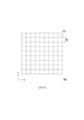
圖1是根據本發明實施例所繪示的電子裝置的示意圖。參考圖1,電子裝置10包括觸控面板100。觸控面板100可例如是投射電容式(Projected capacitive)觸控面板。圖2A是根據本發明圖1實施例所繪示的電子裝置的局部剖面示意圖。一併參考圖2A,圖2A示例性說明在周邊區域A11(A21)中,以線段CL1為剖面線的電子裝置10的部分結構101。
FIG. 1 is a schematic diagram of an electronic device according to an embodiment of the present invention. Referring to FIG. 1 , the electronic device 10 includes a touch panel 100. The touch panel 100 may be, for example, a projected capacitive touch panel. FIG. 2A is a partial cross-sectional schematic diagram of the electronic device according to the embodiment of FIG. 1 of the present invention. Referring to FIG. 2A , FIG. 2A exemplarily illustrates a
在本實施例中,如圖2A所示,電子裝置10還包括顯示面板200。在方向Z上,觸控面板100與顯示面板200相對設置。觸控面板100與顯示面板200之間可透過接合層220互相疊合。接合層220可例如是黏著層或其他功能層。也就是說,在方向Z
上,顯示面板200設置在觸控面板100下方。顯示面板200的顯示面211朝向接合層220以及觸控面板100的第二表面112。顯示面板200可例如是液晶顯示器(liquid crystal display,LCD)、發光二極體(light-emitting diode,LED)、有機發光二極體(Organic Light-Emitting Diode,OLED)、電子紙(EPD)等提供顯示功能的顯示面板。
In this embodiment, as shown in FIG. 2A , the electronic device 10 further includes a
在本實施例中,觸控面板100包括基板110、多個感應電極RX1~RXn、多個驅動電極TX1~TXm、多個第一走線LR1~LR3、多個第二走線LT1~LT4、非透明導電層120、連接器130以及控制器140,其中m、n分別為大於1之正整數。本實施例的感應電極RX1~RXn、驅動電極TX1~TXm、第一走線LR1~LR3以及第二走線LT1~LT4分別的數量僅為範例。
In this embodiment, the touch panel 100 includes a
在本實施例中,基板110包括第一表面111以及第二表面112。在方向Z上,第一表面111相對於第二表面112。在方向X、Y所形成的平面(以下稱為X-Y平面)上,第一表面111包括第一周邊區域A11以及第一主動區域A12,並且第二表面112包括第二周邊區域A21以及第二主動區域A22。在X-Y平面上,第一周邊區域A11環繞第一主動區域A12,並且第二周邊區域A21環繞第二主動區域A22。在方向Z上,第一周邊區域A11相對於第二周邊區域A21,並且第一主動區域A12相對於第二主動區域A22。
In this embodiment, the
在本實施例中,感應電極RX1~RXn以及驅動電極
TX1~TXm分別設置在基板110的不同表面111、112上。詳細而言,感應電極RX1~RXn分別設置於第一表面111上的第一主動區域A12中。驅動電極TX1~TXm分別設置於第二表面112上的第二主動區域A22中。這些感應電極RX1~RXn以及這些驅動電極TX1~TXm可分別例如是氧化銦錫(ITO)電極或其他透明導電材料。
In this embodiment, the sensing electrodes RX1-RXn and the driving electrodes TX1-TXm are respectively disposed on
在本實施例中,感應電極RX1~RXn以及驅動電極TX1~TXm分別在不同的方向上延伸,以形成多條條狀或多條波浪狀的電極。詳細而言,感應電極RX1~RXn分別在Y方向上延伸。驅動電極TX1~TXm分別在X方向上延伸。也就是說,如圖1的X-Y平面所示,驅動電極TX1~TXm在第一表面111上的投影範圍與感應電極RX1~RXn交錯排列,並且感應電極RX1~RXn在第二表面112上的投影範圍與驅動電極TX1~TXm交錯排列。
In this embodiment, the sensing electrodes RX1~RXn and the driving electrodes TX1~TXm extend in different directions to form multiple strip-shaped or multiple wavy electrodes. Specifically, the sensing electrodes RX1~RXn extend in the Y direction. The driving electrodes TX1~TXm extend in the X direction. That is, as shown in the X-Y plane of FIG. 1, the projection range of the driving electrodes TX1~TXm on the
在本實施例中,第一走線LR1~LR3以及第二走線LT1~LT4分別設置在基板110的不同表面111、112上。詳細而言,第一走線LR1~LR3分別設置在第一表面111上的第一周邊區域A11中。第一走線LR1~LR3耦接感應電極RX1~RXn以及連接器130,以傳輸對應的感應信號及/或控制信號。第二走線LT1~LT4分別設置在第二表面112上的第二周邊區域A21中。第二走線LT1~LT4耦接驅動電極TX1~TXm以及連接器130,以傳輸對應的驅動信號及/或控制信號。
In this embodiment, the first traces LR1-LR3 and the second traces LT1-LT4 are respectively arranged on
接續上述的說明,如圖1的X-Y平面所示,第一走線
LR1~LR3以及第二走線LT1~LT4未相互重疊。也就是說,第一走線LR1~LR3在第二表面112上的投影範圍未與第二走線LT1~LT4重疊,並且第二走線LT1~LT4在第一表面111上的投影範圍未與第一走線LR1~LR3重疊。第一走線LR1~LR3以及第二走線LT1~LT4可分別例如是金屬導線。
Continuing with the above description, as shown in the X-Y plane of FIG. 1, the first traces LR1~LR3 and the second traces LT1~LT4 do not overlap with each other. That is, the projection range of the first traces LR1~LR3 on the
在本實施例中,連接器130設置在基板110中及/或基板的表面111、112上。連接器130包括多個金屬接墊131~13k,其中k為大於1之正整數。本實施例的金屬接墊131~13k的數量僅為範例。金屬接墊131~13k分別透過第一走線LR1~LR3以及第二走線LT1~LT4耦接感應電極RX1~RXn以及驅動電極TX1~TXm。金屬接墊131~13k還耦接控制器140。連接器130可例如是軟性印刷電路板(Flexible printed circuit,FPC)。
In this embodiment, the connector 130 is disposed in the
在本實施例中,控制器140設置在基板110中及/或基板的表面111、112上。控制器140包括多個電路(例如是圖3的感應電路341以及驅動電路342)以分別控制感應電極RX1~RXn以及驅動電極TX1~TXm。控制器140可例如是訊號轉換器、現場可程式化邏輯閘陣列(Field Programmable Gate Array,FPGA)、中央處理單元(Central Processing Unit,CPU),或是其他可程式化之一般用途或特殊用途的微處理器(Microprocessor)、數位訊號處理器(Digital Signal Processor,DSP)、可程式化控制器、特殊應用積體電路(Application Specific Integrated Circuits,ASIC)、可程式化邏輯裝置(Programmable Logic Device,PLD)或其他類似裝
置或這些裝置的組合,其可載入並執行電腦程式相關韌體或軟體,以實現控制以及觸控報點等功能。
In this embodiment, the controller 140 is disposed in the
在本實施例中,如圖2A所示,非透明導電層120設置在第二表面112上的第二周邊區域A21中。非透明導電層120可例如是鉬鋁合金結構、鉬鋁鉬結構或其他金屬結構。應注意的是,非透明導電層120在第一表面111的投影範圍涵蓋第一走線LR1~LR3。也就是說,在Z方向上,非透明導電層120與任一個第一走線LR1~LR3重疊。此外,在Z方向上,非透明導電層120位於第一走線LR1~LR3與顯示面板200之間。
In this embodiment, as shown in FIG. 2A , the non-transparent
在此值得一提的是,由於非透明導電層120為導電材料且相對設置在第一走線LR1~LR3與顯示面板200之間,因此非透明導電層120能夠屏蔽顯示面板200或其他鄰近電路所產生的電磁干擾,據以隔絕或降低第一走線LR1~LR3中的雜訊。如此一來,控制器140能夠根據低雜訊的感應信號以及驅動信號來進行觸控報點操作,以增加觸控面板100在操作時的穩定性以及觸控效果。
It is worth mentioning that since the non-transparent
在圖1實施例中,基板110包括陣列排列的多個子觸控區域SA11~SA14、SA21~SA24以及SA31~SA34。本實施例的子觸控區域SA11~SA34的數量僅為範例。也就是說,基板110的主動區域A12(A22)以矩陣的方式被畫分為多個(例如是3 x 4個)子觸控區域SA11~SA34。每一個子觸控區域SA11~SA34可以作為觸控面板300的單元觸控電路(或通道)以進行觸控操作。
In the embodiment of FIG. 1 , the
詳細來說,在方向Y上,子觸控區域SA11、SA12、SA13、 SA14共用相同的感應電極RX1~RX3以及第一走線LR1。也就是說,第一走線LR1耦接在方向Y上排列的多個子觸控區域SA11、SA12、SA13、SA14,其中第一走線LR1耦接感應電極RX1~RXn的一部分(即,前述區域SA11~SA14中的感應電極RX1~RX3)。第一走線LR2、LR3與子觸控區域SA11~SA34的相對關係可以參照前述關於第一走線LR1的相關說明並且加以類推。在本實施例中,第一走線LR1~LR3的數量(例如是3)等於所有子觸控區域SA11~SA34在方向X上的數量(例如是3個子觸控區域SA14、SA24及SA34)。 Specifically, in direction Y, the sub-touch areas SA11, SA12, SA13, and SA14 share the same sensing electrodes RX1-RX3 and the first trace LR1. That is, the first trace LR1 couples the multiple sub-touch areas SA11, SA12, SA13, and SA14 arranged in direction Y, wherein the first trace LR1 couples a portion of the sensing electrodes RX1-RXn (i.e., the sensing electrodes RX1-RX3 in the aforementioned areas SA11-SA14). The relative relationship between the first traces LR2 and LR3 and the sub-touch areas SA11-SA34 can refer to the aforementioned description of the first trace LR1 and be deduced by analogy. In this embodiment, the number of first traces LR1-LR3 (e.g., 3) is equal to the number of all sub-touch areas SA11-SA34 in direction X (e.g., 3 sub-touch areas SA14, SA24, and SA34).
在方向X上,子觸控區域SA11、SA21、SA31共用相同的驅動電極TX1~TX5以及第二走線LT1。也就是說,第二走線LT1耦接在方向X上排列的多個子觸控區域SA11、SA21、SA31,其中第二走線LT1耦接驅動電極TX1~TXm的一部分(即,前述區域SA11~SA31中的驅動電極TX1~TX5)。第二走線LT2~LT4與子觸控區域SA11~SA34的相對關係可以參照前述關於第二走線LT1的相關說明並且加以類推。在本實施例中,第二走線LT1~LT4的數量(例如是4)等於所有子觸控區域SA11~SA34在方向Y上的數量(例如是4個子觸控區域SA11、SA12、SA13及SA14)。 In the direction X, the sub-touch areas SA11, SA21, and SA31 share the same driving electrodes TX1-TX5 and the second trace LT1. In other words, the second trace LT1 couples the multiple sub-touch areas SA11, SA21, and SA31 arranged in the direction X, wherein the second trace LT1 couples a portion of the driving electrodes TX1-TXm (i.e., the driving electrodes TX1-TX5 in the aforementioned areas SA11-SA31). The relative relationship between the second traces LT2-LT4 and the sub-touch areas SA11-SA34 can refer to the aforementioned description of the second trace LT1 and be deduced by analogy. In this embodiment, the number of second traces LT1-LT4 (e.g., 4) is equal to the number of all sub-touch areas SA11-SA34 in direction Y (e.g., 4 sub-touch areas SA11, SA12, SA13, and SA14).
應注意的是,單一個通道(例如是子觸控區域SA11)是多個感應電極RX1~RX3以及多個驅動電極TX1~TX5的組合,據以提高觸控面板100的解析度。此外,由於感應電極RX1~RXn沒有彼此串聯,並且驅動電極TX1~TXm沒有彼此串聯,因此這些通 道(即,子觸控區域SA11~SA34)之間能夠彼此獨立操作。 It should be noted that a single channel (e.g., sub-touch area SA11) is a combination of multiple sensing electrodes RX1~RX3 and multiple driving electrodes TX1~TX5, thereby improving the resolution of the touch panel 100. In addition, since the sensing electrodes RX1~RXn are not connected in series with each other, and the driving electrodes TX1~TXm are not connected in series with each other, these channels (i.e., sub-touch areas SA11~SA34) can operate independently of each other.
圖2B是根據本發明圖1實施例所繪示的電子裝置的局部剖面示意圖。參考圖1以及圖2B,圖2B示例性說明在主動區域A12(A22)中,以線段CL2為剖面線的電子裝置10的部分結構102(即,子觸控區域SA11的剖面結構)。
FIG. 2B is a partial cross-sectional schematic diagram of the electronic device according to the embodiment of FIG. 1 of the present invention. Referring to FIG. 1 and FIG. 2B , FIG. 2B exemplarily illustrates a
在本實施例中,在方向Z上,驅動電極TX3在第一表面111的投影範圍涵蓋感應電極RX1~RX3分別的一部分。也就是說,驅動電極TX3與感應電極RX1~RX3分別的一部分重疊。此外,在Z方向上,驅動電極TX3位於感應電極RX1~RX3與顯示面板200之間。其他的驅動電極TX1~TX2、TX4~TXm與感應電極RX1~RXn的相對結構可以參照驅動電極TX3的相關說明並且加以類推。
In this embodiment, in the direction Z, the projection range of the driving electrode TX3 on the
在本實施例中,如圖2A以及圖2B所示,非透明導電層120以及驅動電極TX3分別設置在第二表面112上的不同區域A21、A22中。也就是說,非透明導電層120與驅動電極TX1~TXm位在相同的平面上(即,相同金屬層中)。
In this embodiment, as shown in FIG. 2A and FIG. 2B , the non-transparent
圖2C是根據本發明圖1實施例所繪示的電子裝置的局部俯視示意圖。參考圖1以及圖2C,圖2C示例性說明在主動區域A12(A22)中電子裝置10的部分結構102。
FIG2C is a partial top view schematic diagram of the electronic device according to the embodiment of FIG1 of the present invention. Referring to FIG1 and FIG2C, FIG2C exemplarily illustrates a
在本實施例中,在X-Y平面上,感應電極RX1在X方向上具有第一寬度W1,並且驅動電極TX1在Y方向上具有第二寬度W2。感應電極RX2~RXn以及驅動電極TX2~TXm可以分別參 照感應電極RX1以及驅動電極TX1的相關說明並且加以類推。 In this embodiment, on the X-Y plane, the sensing electrode RX1 has a first width W1 in the X direction, and the driving electrode TX1 has a second width W2 in the Y direction. The sensing electrodes RX2~RXn and the driving electrodes TX2~TXm can refer to the relevant descriptions of the sensing electrode RX1 and the driving electrode TX1 respectively and by analogy.
應注意的是,第一寬度W1等於第二寬度W2。前述的等於可例如是完全相等,或者是在電極的量測誤差範圍內相等。由於各個感應電極RX1~RXn以及各個驅動電極TX1~TXm具有大致上相同的寬度W1(或W2),因此任意的觸控點與各個感應電極RX1~RXn之間的距離大致上相同,以使這些電極RX1~RXn、TX1~TXm分別能夠獲取大致上相同強度的信號。 It should be noted that the first width W1 is equal to the second width W2. The aforementioned equality can be, for example, completely equal, or equal within the measurement error range of the electrode. Since each sensing electrode RX1~RXn and each driving electrode TX1~TXm has substantially the same width W1 (or W2), the distance between any touch point and each sensing electrode RX1~RXn is substantially the same, so that these electrodes RX1~RXn, TX1~TXm can respectively obtain signals of substantially the same strength.
也就是說,當手指或觸控筆在不同位置進行觸控操作時,這些電極RX1~RXn、TX1~TXm在這些位置上所獲取的多個信號之間的強度變化量不大。如此一來,觸控面板100能夠降低在不同位置上所獲取的多個信號之間的強度變化量,以改善當手指或觸控筆在觸控面板100上移動時這些信號的穩定性以及畫斜線的線性度。 That is, when a finger or a stylus performs a touch operation at different positions, the intensity variation between the multiple signals obtained by these electrodes RX1~RXn, TX1~TXm at these positions is not large. In this way, the touch panel 100 can reduce the intensity variation between the multiple signals obtained at different positions to improve the stability of these signals and the linearity of the diagonal lines when the finger or stylus moves on the touch panel 100.
圖3是根據本發明另一實施例所繪示的電子裝置的示意圖。參考圖3,電子裝置30包括觸控面板300、感應電路341以及驅動電路342。感應電路341以及驅動電路342分別耦接觸控面板300。觸控面板300包括基板(未繪示)、多個感應電極RX1~RX3、多個驅動電極TX1~TX5、多個第一走線(未繪示)、多個第二走線(未繪示)以及非透明導電層(未繪示)。本實施例的電極RX1~RX3、TX1~TX5分別的數量僅為範例。觸控面板300以及觸控面板300所包括的元件可以參照觸控面板100的相關說明並且加以類推。
FIG3 is a schematic diagram of an electronic device according to another embodiment of the present invention. Referring to FIG3 , the
在本實施例中,在X-Y平面上,相鄰的任二個感應電極 (例如是RX2、RX3)之間在X方向上具有第一間隙G1。也就是說,在X方向上,感應電極RX1~RX3以相同的第一間隙G1依序間隔排列。此外,各個感應電極(例如是RX3)在X方向上具有第一寬度W1。在本實施例中,第一間隙G1小於第一寬度W1。 In this embodiment, on the X-Y plane, there is a first gap G1 between any two adjacent sensing electrodes (e.g., RX2 and RX3) in the X direction. That is, in the X direction, the sensing electrodes RX1 to RX3 are arranged in sequence with the same first gap G1. In addition, each sensing electrode (e.g., RX3) has a first width W1 in the X direction. In this embodiment, the first gap G1 is smaller than the first width W1.
在本實施例中,在X-Y平面上,相鄰的任二個驅動電極(例如是TX1、TX2)之間在Y方向上具有第二間隙G2。也就是說,在Y方向上,驅動電極TX1~TX5以相同的第二間隙G2依序間隔排列。此外,各個驅動電極(例如是TX1)在Y方向上具有第二寬度W2。在本實施例中,第二間隙G2小於第二寬度W2。 In this embodiment, on the X-Y plane, there is a second gap G2 between any two adjacent drive electrodes (e.g., TX1, TX2) in the Y direction. That is, in the Y direction, the drive electrodes TX1 to TX5 are arranged in sequence with the same second gap G2. In addition, each drive electrode (e.g., TX1) has a second width W2 in the Y direction. In this embodiment, the second gap G2 is smaller than the second width W2.
在本實施例中,第一間隙G1大於第二間隙G2。這些間隙G1、G2分別可例如在15微米(μm)至30微米的範圍內。此外,第一寬度W1大致上等於第二寬度W2。也就是說,在X-Y平面上,感應電極RX1~RX3以及驅動電極TX1~TX5分別以不同的密度排列。在本實施例中,感應電極RX1~RX3的數量小於驅動電極TX1~TX5的數量。在一些實施例中,感應電極RX1~RX3以及驅動電極TX1~TX5分別的數量取決於觸控面板300的主動區域(例如是圖1的主動區域A12(A22)的尺寸。 In this embodiment, the first gap G1 is larger than the second gap G2. These gaps G1 and G2 may be, for example, in the range of 15 micrometers (μm) to 30 micrometers. In addition, the first width W1 is substantially equal to the second width W2. That is, on the X-Y plane, the sensing electrodes RX1~RX3 and the driving electrodes TX1~TX5 are arranged at different densities. In this embodiment, the number of sensing electrodes RX1~RX3 is less than the number of driving electrodes TX1~TX5. In some embodiments, the number of sensing electrodes RX1~RX3 and the number of driving electrodes TX1~TX5 depends on the size of the active area of the touch panel 300 (for example, the active area A12 (A22) of Figure 1).
在本實施例中,感應電路341透過多個第一走線分別耦接感應電極RX1~RX3。感應電路341輸出多個控制信號至感應電極RX1~RX3。感應電路341接收並處理感應電極RX1~RX3所獲取的多個感應信號。在本實施例中,驅動電路342透過多個第二走線分別耦接驅動電極TX1~TX5。驅動電路342輸出多個控制信
號至驅動電極TX1~TX5。驅動電路342接收並處理驅動電極TX1~TX5所獲取的多個驅動信號。
In this embodiment, the
在本實施例中,感應電路341與驅動電路342配置在不同的晶片中。在一些實施例中,感應電路341與驅動電路342整合在相同的晶片中(例如是圖1的控制器140)。
In this embodiment, the
圖4是根據本發明另一實施例所繪示的電子裝置的示意圖。參考圖4,電子裝置40包括觸控面板400以及顯示面板(未繪示)。觸控面板400包括基板(未繪示)、多個感應電極RX1~RXn、多個驅動電極TX1~TXm、多個第一走線LR11~LR41、LR12~LR42、多個第二走線LT11~LT61、非透明導電層(未繪示)、連接器430以及控制器(未繪示)。本實施例的感應電極RX1~RXn、驅動電極TX1~TXm、第一走線LR11~LR41、LR12~LR42以及第二走線LT1~LT6分別的數量僅為範例。觸控面板400以及觸控面板400所包括的元件可以參照觸控面板100的相關說明並且加以類推。
FIG. 4 is a schematic diagram of an electronic device according to another embodiment of the present invention. Referring to FIG. 4 , the
在本實施例中,第一走線LR11~LR42的一部分(例如是第一走線LR11、LR21、LR31、LR41)以及另一部分(例如是第一走線LR12、LR22、LR32、LR42)分別耦接感應電極RX1~RXn的多個起始端以及多個末端。前述的起始端以及末端可例如是在方向Y上相對的二端。也就是說,在方向Y上,感應電極RX1~RX3在周邊區域A11(A21)中兩側的起始端以及末端分別搭接第一走線LR11以及LR12。前述的這些走線LR11、LR12進一步被集中以搭接至連接器430。其他第一走線LR21~LR42與感應電極
RX1~RXn的相對關係可以參照前述關於第一走線LR11、LR12的相關說明並且加以類推。
In this embodiment, a portion of the first traces LR11-LR42 (e.g., the first traces LR11, LR21, LR31, LR41) and another portion (e.g., the first traces LR12, LR22, LR32, LR42) are coupled to multiple starting ends and multiple endings of the sensing electrodes RX1-RXn, respectively. The aforementioned starting ends and endings may be, for example, two ends opposite to each other in the direction Y. That is, in the direction Y, the starting ends and endings of the sensing electrodes RX1-RX3 on both sides of the peripheral area A11 (A21) are respectively connected to the first traces LR11 and LR12. The aforementioned traces LR11 and LR12 are further concentrated to be connected to the
應注意的是,由於第一走線LR11、LR12並聯於感應電極RX1~RX3,因此感應電極RX1~RX3所對應的通道(可例如是圖1的各個子觸控區域SA11~SA14)的阻抗能夠被降低。如此一來,透過感應電極RX1~RXn為雙邊走線的設計,能夠降低各個通道的阻抗,以減少觸控面板400操作時的電阻電容負載(RC loading)。
It should be noted that since the first traces LR11 and LR12 are connected in parallel to the sensing electrodes RX1 to RX3, the impedance of the channels corresponding to the sensing electrodes RX1 to RX3 (such as the sub-touch areas SA11 to SA14 in FIG. 1 ) can be reduced. In this way, by designing the sensing electrodes RX1 to RXn as double-sided traces, the impedance of each channel can be reduced to reduce the RC loading when the
在一些實施例中,第二走線的一部分(例如是圖4所示的第二走線LT11~LT61)以及另一部分(未繪示)分別耦接驅動電極TX1~TXm的多個起始端以及多個末端。前述的起始端以及末端可例如是在方向X上相對的二端。也就是說,在方向X上,驅動電極TX1~TX4在周邊區域A11(A21)中兩側的起始端以及末端分別搭接第二走線LT11以及另一條第二走線(未繪示)。前述的這些第二走線LT11進一步被集中以搭接至連接器430。其他第二走線LT11~LT61與驅動電極TX1~TXm的相對關係可以參照前述關於第二走線LT11的相關說明並且加以類推。
In some embodiments, a portion of the second trace (e.g., the second traces LT11 to LT61 shown in FIG. 4 ) and another portion (not shown) are respectively coupled to multiple starting ends and multiple endings of the driving electrodes TX1 to TXm. The aforementioned starting end and ending may be, for example, two opposite ends in direction X. That is, in direction X, the starting ends and endings of the driving electrodes TX1 to TX4 on both sides of the peripheral area A11 (A21) are respectively connected to the second trace LT11 and another second trace (not shown). The aforementioned second traces LT11 are further concentrated to be connected to the
應注意的是,由於第二走線LT11以及另一條未繪示的第二走線並聯於驅動電極TX1~TX4,因此驅動電極TX1~TX4所對應的通道(可例如是圖1的各個子觸控區域SA11~SA31)的阻抗能夠被降低,並據以減少觸控面板400操作時的電阻電容負載。
It should be noted that since the second trace LT11 and another second trace not shown are connected in parallel to the driving electrodes TX1-TX4, the impedance of the channel corresponding to the driving electrodes TX1-TX4 (such as the sub-touch areas SA11-SA31 in FIG. 1) can be reduced, thereby reducing the resistance and capacitance load of the
在另一方面,在觸控面板400的組裝過程中,假使任意個感應電極RX1~RXn及/或驅動電極TX1~TXm被刮傷時,透過
並聯的其他電極RX1~RXn及/或TX1~TXm能夠使觸控面板400正常操作,據以提高電子裝置40的穩定性。
On the other hand, during the assembly process of the
在本實施例中,在X-Y平面上,感應電極RX1~RXn在X方向上具有相同的寬度(未標示)。在X-Y平面上,驅動電極TX1~TXm在Y方向上具有不同的寬度(未標示)。感應電極RX1~RXn的寬度大於或(大致上)等於驅動電極TX1~TXm的多個寬度。 In this embodiment, on the X-Y plane, the sensing electrodes RX1-RXn have the same width in the X direction (not marked). On the X-Y plane, the driving electrodes TX1-TXm have different widths in the Y direction (not marked). The width of the sensing electrodes RX1-RXn is greater than or (substantially) equal to the multiple widths of the driving electrodes TX1-TXm.
圖5A至圖5B是根據本發明圖4實施例所繪示的電子裝置的局部剖面示意圖。參考圖4至圖5B,圖5A以及圖2B分別示例性說明在主動區域A12(A22)中電子裝置40在不同金屬層(或剖面層)的部分結構402。
Figures 5A to 5B are partial cross-sectional schematic diagrams of the electronic device according to the embodiment of Figure 4 of the present invention. Referring to Figures 4 to 5B, Figures 5A and 2B respectively illustrate the
圖5A實施例示例性說明設置在基板400的第二表面上的第一層的部分結構402。圖5B實施例示例性說明設置在基板400的第二表面上的第二層的部分結構402。前述的第一層與第二層可以是在Z方向上相鄰的不同金屬層(或剖面層)。也就是說,在Z方向上,圖5A所示的部分結構402以及圖5B所示的部分結構402互相重合。
FIG5A exemplarily illustrates a
在本實施例中,觸控面板400還包括設置在主動區域A12(A22)中的非透明導電層520。如圖5B所示,非透明導電層520設置在第二表面上的第二主動區域A22中。非透明導電層520可例如是鉬鋁合金結構、鉬鋁鉬結構或其他金屬結構。應注意的是,非透明導電層520是經過圖形化而形成網狀格結構或波浪狀結構。
考量人眼視覺效果,非透明導電層520的線寬可例如在1.5微米至3微米的範圍內,並且非透明導電層520在X方向或Y方向的間距W3可例如在200微米至1500微米的範圍內。
In this embodiment, the
在本實施例中,如圖5A至圖5B的X-Y平面所示,多個驅動電極TXm以及非透明導電層520相互重疊。也就是說,非透明導電層520在第二表面上的投影範圍涵蓋多個驅動電極TXm。由於非透明導電層520在Z方向上與多個驅動電極TXm重疊以相互耦接,因此觸控面板400的阻抗能夠被降低。
In this embodiment, as shown in the X-Y plane of FIG. 5A to FIG. 5B, a plurality of driving electrodes TXm and a non-transparent
綜上所述,本發明實施例的電子裝置是將非透明導電層設置在耦接感應電極的多個走線的相對面上,非透明導電層能夠屏蔽顯示面板對這些走線造成的電磁干擾,以降低雜訊並提高觸控面板操作時的穩定度。在部分實施例中,多個感應電極以及多個驅動電極可以構成單一個子觸控區域(即,通道),此通道能夠獨立操作並提高觸控面板的解析度。在部分實施例中,透過感應電極與驅動電極具有相同的寬度,能夠降低不同位置上信號之間的強度變化量,以提高觸控面板操作時的穩定度。在部分實施例中,感應電極及/或驅動電極的二端分別搭接走線,據以降低各個通道的阻抗並減少觸控面板操作時的電阻電容負載。 In summary, the electronic device of the embodiment of the present invention is to set a non-transparent conductive layer on the opposite surface of multiple wirings coupled to the sensing electrode. The non-transparent conductive layer can shield the electromagnetic interference caused by the display panel to these wirings to reduce noise and improve the stability of the touch panel during operation. In some embodiments, multiple sensing electrodes and multiple driving electrodes can constitute a single sub-touch area (i.e., channel), which can operate independently and improve the resolution of the touch panel. In some embodiments, by having the sensing electrode and the driving electrode have the same width, the intensity variation between signals at different positions can be reduced to improve the stability of the touch panel during operation. In some embodiments, the two ends of the sensing electrode and/or the driving electrode are respectively connected to the wiring to reduce the impedance of each channel and reduce the resistance and capacitance load when the touch panel is operated.
雖然本發明已以實施例揭露如上,然其並非用以限定本發明,任何所屬技術領域中具有通常知識者,在不脫離本發明的精神和範圍內,當可作些許的更動與潤飾,故本發明的保護範圍當視後附的申請專利範圍所界定者為準。 Although the present invention has been disclosed as above by the embodiments, it is not intended to limit the present invention. Anyone with ordinary knowledge in the relevant technical field can make some changes and modifications without departing from the spirit and scope of the present invention. Therefore, the protection scope of the present invention shall be subject to the scope defined by the attached patent application.
10:電子裝置
100:觸控面板
101、102:部分結構
130:連接器
131~13k:金屬接墊
140:控制器
A11、A21:周邊區域
A12、A22:主動區域
CL1、CL2:線段
LR1~LR3:第一走線
LT1~LT4:第二走線
RX1~RXn:感應電極
SA11~SA34:子觸控區域
TX1~TXm:驅動電極
X、Y:方向
10: Electronic device
100:
Claims (21)
Priority Applications (2)
| Application Number | Priority Date | Filing Date | Title |
|---|---|---|---|
| TW112102963A TWI856497B (en) | 2023-01-30 | 2023-01-30 | Electronic device |
| US18/303,554 US12079418B2 (en) | 2023-01-30 | 2023-04-19 | Electronic device enhancing stability and touch sensing effects |
Applications Claiming Priority (1)
| Application Number | Priority Date | Filing Date | Title |
|---|---|---|---|
| TW112102963A TWI856497B (en) | 2023-01-30 | 2023-01-30 | Electronic device |
Publications (2)
| Publication Number | Publication Date |
|---|---|
| TW202431083A TW202431083A (en) | 2024-08-01 |
| TWI856497B true TWI856497B (en) | 2024-09-21 |
Family
ID=91964483
Family Applications (1)
| Application Number | Title | Priority Date | Filing Date |
|---|---|---|---|
| TW112102963A TWI856497B (en) | 2023-01-30 | 2023-01-30 | Electronic device |
Country Status (2)
| Country | Link |
|---|---|
| US (1) | US12079418B2 (en) |
| TW (1) | TWI856497B (en) |
Citations (3)
| Publication number | Priority date | Publication date | Assignee | Title |
|---|---|---|---|---|
| CN103744568A (en) * | 2014-01-13 | 2014-04-23 | 深圳莱宝高科技股份有限公司 | Touch panel and manufacturing method thereof |
| TWM515149U (en) * | 2014-07-30 | 2016-01-01 | Lg伊諾特股份有限公司 | Touch panel |
| TW201610796A (en) * | 2014-09-05 | 2016-03-16 | 勝華科技股份有限公司 | Touch panel and touch display device |
Family Cites Families (7)
| Publication number | Priority date | Publication date | Assignee | Title |
|---|---|---|---|---|
| US7920129B2 (en) | 2007-01-03 | 2011-04-05 | Apple Inc. | Double-sided touch-sensitive panel with shield and drive combined layer |
| TWI408451B (en) | 2010-01-21 | 2013-09-11 | Wintek Corp | Touch display panel |
| US9529479B2 (en) | 2011-10-14 | 2016-12-27 | Hung-Ta LIU | Touch sensing method, module, and display |
| JP6396478B2 (en) | 2013-09-27 | 2018-09-26 | センセル インコーポレイテッドSensel,Inc. | Touch sensor detection system and method |
| TWI562042B (en) | 2015-10-21 | 2016-12-11 | Focaltech Systems Co Ltd | Touch display device and drivinig method thereof |
| JP6815173B2 (en) | 2016-11-17 | 2021-01-20 | 株式会社ジャパンディスプレイ | Touch sensor and display device |
| JP6463877B1 (en) * | 2017-08-01 | 2019-02-06 | 株式会社ワコム | Sensor for detecting the pen signal sent by the pen |
-
2023
- 2023-01-30 TW TW112102963A patent/TWI856497B/en active
- 2023-04-19 US US18/303,554 patent/US12079418B2/en active Active
Patent Citations (3)
| Publication number | Priority date | Publication date | Assignee | Title |
|---|---|---|---|---|
| CN103744568A (en) * | 2014-01-13 | 2014-04-23 | 深圳莱宝高科技股份有限公司 | Touch panel and manufacturing method thereof |
| TWM515149U (en) * | 2014-07-30 | 2016-01-01 | Lg伊諾特股份有限公司 | Touch panel |
| TW201610796A (en) * | 2014-09-05 | 2016-03-16 | 勝華科技股份有限公司 | Touch panel and touch display device |
Also Published As
| Publication number | Publication date |
|---|---|
| US20240256076A1 (en) | 2024-08-01 |
| TW202431083A (en) | 2024-08-01 |
| US12079418B2 (en) | 2024-09-03 |
Similar Documents
| Publication | Publication Date | Title |
|---|---|---|
| US8497430B2 (en) | Display device | |
| KR101447738B1 (en) | Touch window | |
| TWI422907B (en) | Touch panel | |
| TWI480775B (en) | Touch panel and manufacturing method thereof | |
| TW201508568A (en) | Touch display device | |
| TWM461834U (en) | Touch panel | |
| US11579737B2 (en) | Touch substrate and touch display device | |
| CN103135831B (en) | touch panel | |
| TW201512914A (en) | Touch control panel and touch display device | |
| TWI620103B (en) | Touch panel | |
| TWI489335B (en) | Conductive substrate and touch panel | |
| WO2020156234A1 (en) | Touch screen for narrow-bezel electronic apparatus, and electronic apparatus | |
| TWI570617B (en) | Capacitive Touch Apparatus | |
| TW201510811A (en) | Touch panel and manufacturing process thereof | |
| KR101357591B1 (en) | Touch window having reinforcing pad | |
| TWI856497B (en) | Electronic device | |
| KR101926622B1 (en) | Touch window | |
| TWI485605B (en) | Touch panel | |
| TWI699680B (en) | Touch panel and touch display device using same | |
| KR20150066860A (en) | Touch sensor integrated type flat panel display | |
| KR20150057323A (en) | Touch sensor integrated type display device with narrow bezel area | |
| KR20140079994A (en) | Touch sensor integrated type display device | |
| TWI549574B (en) | Substrate structure | |
| CN118409669A (en) | Electronic device | |
| KR101259843B1 (en) | Touch window having duoble ruoting circuit |