TWI788570B - Reflection-mode electron-beam inspection using ptychographic imaging - Google Patents

Reflection-mode electron-beam inspection using ptychographic imaging Download PDF

Info

Publication number
TWI788570B
TWI788570B TW108117595A TW108117595A TWI788570B TW I788570 B TWI788570 B TW I788570B TW 108117595 A TW108117595 A TW 108117595A TW 108117595 A TW108117595 A TW 108117595A TW I788570 B TWI788570 B TW I788570B
Authority
TW
Taiwan
Prior art keywords
sample
particle beam
selected portions
images
plane images
Prior art date
Application number
TW108117595A
Other languages
Chinese (zh)
Other versions
TW202012922A (en
Inventor
黃偉杰
Original Assignee
美商克萊譚克公司
Priority date (The priority date is an assumption and is not a legal conclusion. Google has not performed a legal analysis and makes no representation as to the accuracy of the date listed.)
Filing date
Publication date
Application filed by 美商克萊譚克公司 filed Critical 美商克萊譚克公司
Publication of TW202012922A publication Critical patent/TW202012922A/en
Application granted granted Critical
Publication of TWI788570B publication Critical patent/TWI788570B/en

Links

Images

Classifications

    • HELECTRICITY
    • H01ELECTRIC ELEMENTS
    • H01JELECTRIC DISCHARGE TUBES OR DISCHARGE LAMPS
    • H01J37/00Discharge tubes with provision for introducing objects or material to be exposed to the discharge, e.g. for the purpose of examination or processing thereof
    • H01J37/26Electron or ion microscopes; Electron or ion diffraction tubes
    • H01J37/29Reflection microscopes
    • HELECTRICITY
    • H01ELECTRIC ELEMENTS
    • H01JELECTRIC DISCHARGE TUBES OR DISCHARGE LAMPS
    • H01J37/00Discharge tubes with provision for introducing objects or material to be exposed to the discharge, e.g. for the purpose of examination or processing thereof
    • H01J37/26Electron or ion microscopes; Electron or ion diffraction tubes
    • H01J37/29Reflection microscopes
    • H01J37/292Reflection microscopes using scanning ray
    • GPHYSICS
    • G06COMPUTING OR CALCULATING; COUNTING
    • G06TIMAGE DATA PROCESSING OR GENERATION, IN GENERAL
    • G06T12/00Tomographic reconstruction from projections
    • G06T12/20Inverse problem, i.e. transformations from projection space into object space
    • GPHYSICS
    • G06COMPUTING OR CALCULATING; COUNTING
    • G06TIMAGE DATA PROCESSING OR GENERATION, IN GENERAL
    • G06T3/00Geometric image transformations in the plane of the image
    • G06T3/40Scaling of whole images or parts thereof, e.g. expanding or contracting
    • G06T3/4053Scaling of whole images or parts thereof, e.g. expanding or contracting based on super-resolution, i.e. the output image resolution being higher than the sensor resolution
    • HELECTRICITY
    • H01ELECTRIC ELEMENTS
    • H01JELECTRIC DISCHARGE TUBES OR DISCHARGE LAMPS
    • H01J37/00Discharge tubes with provision for introducing objects or material to be exposed to the discharge, e.g. for the purpose of examination or processing thereof
    • H01J37/02Details
    • H01J37/04Arrangements of electrodes and associated parts for generating or controlling the discharge, e.g. electron-optical arrangement or ion-optical arrangement
    • H01J37/147Arrangements for directing or deflecting the discharge along a desired path
    • H01J37/1472Deflecting along given lines
    • H01J37/1474Scanning means
    • H01J37/1475Scanning means magnetic
    • HELECTRICITY
    • H01ELECTRIC ELEMENTS
    • H01JELECTRIC DISCHARGE TUBES OR DISCHARGE LAMPS
    • H01J37/00Discharge tubes with provision for introducing objects or material to be exposed to the discharge, e.g. for the purpose of examination or processing thereof
    • H01J37/02Details
    • H01J37/22Optical, image processing or photographic arrangements associated with the tube
    • H01J37/222Image processing arrangements associated with the tube
    • HELECTRICITY
    • H01ELECTRIC ELEMENTS
    • H01JELECTRIC DISCHARGE TUBES OR DISCHARGE LAMPS
    • H01J37/00Discharge tubes with provision for introducing objects or material to be exposed to the discharge, e.g. for the purpose of examination or processing thereof
    • H01J37/26Electron or ion microscopes; Electron or ion diffraction tubes
    • H01J37/261Details
    • GPHYSICS
    • G06COMPUTING OR CALCULATING; COUNTING
    • G06TIMAGE DATA PROCESSING OR GENERATION, IN GENERAL
    • G06T2211/00Image generation
    • G06T2211/40Computed tomography
    • G06T2211/424Iterative
    • HELECTRICITY
    • H01ELECTRIC ELEMENTS
    • H01JELECTRIC DISCHARGE TUBES OR DISCHARGE LAMPS
    • H01J2237/00Discharge tubes exposing object to beam, e.g. for analysis treatment, etching, imaging
    • H01J2237/22Treatment of data
    • H01J2237/226Image reconstruction
    • HELECTRICITY
    • H01ELECTRIC ELEMENTS
    • H01JELECTRIC DISCHARGE TUBES OR DISCHARGE LAMPS
    • H01J2237/00Discharge tubes exposing object to beam, e.g. for analysis treatment, etching, imaging
    • H01J2237/26Electron or ion microscopes
    • H01J2237/2614Holography or phase contrast, phase related imaging in general, e.g. phase plates

Landscapes

  • Chemical & Material Sciences (AREA)
  • Analytical Chemistry (AREA)
  • Engineering & Computer Science (AREA)
  • Physics & Mathematics (AREA)
  • General Physics & Mathematics (AREA)
  • Theoretical Computer Science (AREA)
  • Computer Vision & Pattern Recognition (AREA)
  • Analysing Materials By The Use Of Radiation (AREA)
  • Algebra (AREA)
  • Mathematical Analysis (AREA)
  • Mathematical Optimization (AREA)
  • Mathematical Physics (AREA)
  • Pure & Applied Mathematics (AREA)

Abstract

A particle-beam inspection system may include a reflective particle-beam imaging system providing an image of a selected portion of a sample and a diffraction pattern of the selected portion of the sample and a controller communicatively coupled to the reflective particle-beam imaging system. The controller may receive two or more sample-plane images from the reflective particle-beam imaging system associated with two or more selected portions of the sample, where at least some of the two or more selected portions of the sample overlap. The controller may further receive two or more diffraction-plane images from the reflective particle-beam imaging system associated with the two or more selected portions of the sample. The controller may further construct one or more output images of the two or more selected portions of the sample from the two or more diffraction-plane images using phase information obtained from the two or more sample-plane images.

Description

使用疊層成像之反射模式電子束檢測Reflection Mode Electron Beam Inspection Using Stack Imaging

本發明大體上係關於半導體檢測,且更特定而言,本發明係關於使用電子束之半導體檢測。The present invention relates generally to semiconductor inspection, and more particularly, the present invention relates to semiconductor inspection using electron beams.

檢測度量常用於評估及/或控制整個半導體製程中之各個程序步驟。通常期望依一高通量提供高解析度檢測以提供足以用於可接受通量要求內之評估及/或控制之資料。各種檢測技術提供解析度與通量之間的不同權衡且因此可戰略性用於一檢測程序內。然而,提供更小及更複雜裝置之先進製造技術需要同等先進之檢測技術來維持一所要通量。因此,期望提供用於精確及高效率檢測之系統及方法。Inspection metrics are commonly used to evaluate and/or control various process steps throughout the semiconductor manufacturing process. It is generally desirable to provide high resolution detection at a high throughput to provide sufficient data for evaluation and/or control within acceptable throughput requirements. Various detection technologies offer different trade-offs between resolution and throughput and thus can be used strategically within a detection program. However, advanced manufacturing techniques that provide smaller and more complex devices require equally advanced detection techniques to maintain a desired throughput. Therefore, it is desirable to provide systems and methods for accurate and efficient detection.

根據本發明之一或多個說明性實施例,揭示一種粒子束檢測系統。在一說明性實施例中,該系統包含提供一樣本之一選定部分之一影像及該樣本之該選定部分之一繞射圖案的一反射粒子束成像系統。在另一說明性實施例中,該系統包含通信耦合至該反射粒子束成像系統之一控制器。在另一說明性實施例中,該控制器自該反射粒子束成像系統接收與該樣本之兩個或兩個以上選定部分相關聯之兩個或兩個以上樣本平面影像,其中該樣本之該兩個或兩個以上選定部分之至少若干者重疊。在另一說明性實施例中,該控制器自該反射粒子束成像系統接收與該樣本之該兩個或兩個以上選定部分相關聯之兩個或兩個以上繞射平面影像。在另一說明性實施例中,該控制器使用自該兩個或兩個以上樣本平面影像獲得之相位資訊來使該樣本之該兩個或兩個以上選定部分之一或多個輸出影像由該兩個或兩個以上繞射平面影像建構。In accordance with one or more illustrative embodiments of the invention, a particle beam detection system is disclosed. In an illustrative embodiment, the system includes a reflective particle beam imaging system that provides an image of a selected portion of a sample and a diffraction pattern of the selected portion of the sample. In another illustrative embodiment, the system includes a controller communicatively coupled to the reflective particle beam imaging system. In another illustrative embodiment, the controller receives two or more sample plane images associated with two or more selected portions of the sample from the reflective particle beam imaging system, wherein the At least some of two or more selected portions overlap. In another illustrative embodiment, the controller receives two or more diffraction plane images associated with the two or more selected portions of the sample from the reflective particle beam imaging system. In another illustrative embodiment, the controller uses phase information obtained from the two or more sample plane images to cause one or more output images of the two or more selected portions of the sample to be generated by The two or more diffraction plane images are constructed.

根據本發明之一或多個說明性實施例,揭示一種粒子束檢測系統。在一說明性實施例中,該系統包含通信耦合至一反射粒子束成像系統之一控制器,該反射粒子束成像系統提供一樣本之一選定部分之一影像及該樣本之該選定部分之一繞射圖案。在另一說明性實施例中,該控制器自該反射粒子束成像系統接收與該樣本之兩個或兩個以上選定部分相關聯之兩個或兩個以上樣本平面影像,其中該樣本之該兩個或兩個以上選定部分之至少若干者重疊。在另一說明性實施例中,該控制器自該反射粒子束成像系統接收與該樣本之該兩個或兩個以上選定部分相關聯之兩個或兩個以上繞射平面影像。在另一說明性實施例中,該控制器使用自該兩個或兩個以上樣本平面影像獲得之相位資訊來使該樣本之該兩個或兩個以上選定部分之一或多個輸出影像由該兩個或兩個以上繞射平面影像建構。In accordance with one or more illustrative embodiments of the invention, a particle beam detection system is disclosed. In an illustrative embodiment, the system includes a controller communicatively coupled to a reflective particle beam imaging system that provides an image of a selected portion of a sample and one of the selected portions of the sample Diffraction pattern. In another illustrative embodiment, the controller receives two or more sample plane images associated with two or more selected portions of the sample from the reflective particle beam imaging system, wherein the At least some of two or more selected portions overlap. In another illustrative embodiment, the controller receives two or more diffraction plane images associated with the two or more selected portions of the sample from the reflective particle beam imaging system. In another illustrative embodiment, the controller uses phase information obtained from the two or more sample plane images to cause one or more output images of the two or more selected portions of the sample to be generated by The two or more diffraction plane images are constructed.

根據本發明之一或多個說明性實施例,揭示一種檢測方法。在一說明性實施例中,該方法包含自反射粒子束成像系統接收與樣本之兩個或兩個以上選定部分相關聯之兩個或兩個以上樣本平面影像,其中該樣本之該兩個或兩個以上選定部分之至少若干者重疊。在另一說明性實施例中,該方法包含自該反射粒子束成像系統接收與該樣本之該兩個或兩個以上選定部分相關聯之兩個或兩個以上繞射平面影像。在另一說明性實施例中,該方法包含使用自該兩個或兩個以上樣本平面影像獲得之相位資訊來使該樣本之該兩個或兩個以上選定部分之一或多個輸出影像由該兩個或兩個以上繞射平面影像建構。According to one or more illustrative embodiments of the invention, a method of detection is disclosed. In an illustrative embodiment, the method includes receiving two or more sample plane images associated with two or more selected portions of a sample from a reflective particle beam imaging system, wherein the two or more selected portions of the sample are At least some of the two or more selected parts overlap. In another illustrative embodiment, the method includes receiving two or more diffraction plane images associated with the two or more selected portions of the sample from the reflective particle beam imaging system. In another illustrative embodiment, the method includes using phase information obtained from the two or more sample plane images to cause one or more output images of the two or more selected portions of the sample to be generated by The two or more diffraction plane images are constructed.

應瞭解,以上一般描述及以下詳細描述兩者僅供例示及說明且未必限制本發明。併入本說明書中且構成本說明書之一部分之附圖繪示本發明之實施例且與一般描述一起用於解釋本發明之原理。It is to be understood that both the foregoing general description and the following detailed description are illustrative and explanatory only and are not necessarily restrictive of the invention. The accompanying drawings, which are incorporated in and constitute a part of this specification, illustrate the embodiments of the invention and together with the general description serve to explain the principles of the invention.

相關申請案之交叉參考 本申請案根據35 U.S.C. § 119(e)主張名叫Weijie (Jason) Huang之發明者在2018年5月23日以名稱「HIGH SPEED ELECTRON INSPECTION APPARATUS USING PTYCHOGRAPHIC IMAGING」申請之美國臨時申請案第62/675,645號之權利,該案之全文以引用的方式併入本文中。Cross References to Related Applications This application claims under 35 U.S.C. § 119(e) U.S. Provisional Application No. 62/ filed on May 23, 2018 under the title "HIGH SPEED ELECTRON INSPECTION APPARATUS USING PTYCHOGRAPHIC IMAGING" by an inventor named Weijie (Jason) Huang 675,645, which is hereby incorporated by reference in its entirety.

現將詳細參考附圖中所繪示之揭示標的。已相對於特定實施例及其特定特徵來特別展示及描述本發明。本文中所闡釋之實施例應被視為說明而非限制。一般技術者應易於明白,可在不背離本發明之精神及範疇之情況下對形式及細節進行各種改變及修改。Reference will now be made in detail to the disclosed subject matter illustrated in the accompanying drawings. The invention has been particularly shown and described with respect to certain embodiments and certain features thereof. The embodiments set forth herein are to be considered illustrative rather than limiting. It will be readily apparent to those skilled in the art that various changes and modifications in form and detail can be made without departing from the spirit and scope of the invention.

本發明之實施例係針對在適合於檢測半導體裝置之一反射模式組態中使用高效率高解析度檢測之粒子束來疊層成像之系統及方法。在一些實施例中,反射疊層成像藉由基於疊層技術使用來自樣本平面影像之相位資訊變換包含樣本之繞射圖案之繞射平面影像來產生樣本之高解析度輸出影像。就此而言,繞射成像及疊層成像之組合可提供具有比直接產生之樣本平面影像高之解析度之輸出影像。Embodiments of the present invention are directed to systems and methods for stack imaging using particle beams for high-efficiency high-resolution detection in a reflection-mode configuration suitable for inspection of semiconductor devices. In some embodiments, reflection stack imaging produces a high resolution output image of a sample by transforming a diffraction plane image containing a diffraction pattern of the sample using phase information from the sample plane image based on stacking techniques. In this regard, the combination of diffractive imaging and lamination imaging can provide an output image with higher resolution than directly produced sample plane images.

基於成像之檢測系統通常藉由產生一樣本之一影像且比較該影像與一參考(其可包含一參考樣本之一影像、一模擬影像、設計資料或其類似者)來特徵化該樣本。可透過各種技術來產生一樣本影像。例如,一掃描成像系統可藉由使一緊聚焦檢測束(例如一粒子束、一光束或其類似者)掃描樣本且使用一單像素偵測器對自樣本發出之捕獲輻射(例如電子、光子或其類似者)取樣以逐像素構建影像來產生一影像。舉另一實例而言,一投影成像系統可照射樣本上之一相對較大區域(例如一視域)且在一多像素偵測器上產生整個視域之一影像。Imaging-based inspection systems typically characterize a sample by generating an image of the sample and comparing the image to a reference (which may include an image of a reference sample, a simulated image, design data, or the like). A sample image can be generated by various techniques. For example, a scanning imaging system can scan a sample by scanning a tightly focused detection beam (e.g., a particle beam, a light beam, or the like) and using a single-pixel detector to capture radiation (e.g., electrons, photons, etc.) emanating from the sample. or the like) to construct an image pixel by pixel to generate an image. As another example, a projection imaging system can illuminate a relatively large area on a sample (eg, a field of view) and produce an image of the entire field of view on a multi-pixel detector.

在此應認識到,投影成像歸因於在一既定時間特徵化相對較大樣本區域而提供相對高於掃描成像之通量,但可提供較低解析度。一掃描成像系統之解析度通常受限於照明束之聚焦光點大小。因此,高解析度掃描系統通常使用適合於緊聚焦之粒子束(例如電子束、離子束、中性粒子束或其類似者)。相比而言,成像元件之像差(例如球面像差、色像差及其類似者)通常限制投影成像系統之解析度及/或視域。It should be appreciated here that projection imaging provides relatively higher throughput than scanning imaging due to characterizing a relatively larger sample area at a given time, but may provide lower resolution. The resolution of a scanning imaging system is usually limited by the focused spot size of the illumination beam. Accordingly, high-resolution scanning systems typically use particle beams (eg, electron beams, ion beams, neutral particle beams, or the like) that are suitable for tight focusing. In contrast, aberrations of imaging elements, such as spherical aberration, chromatic aberration, and the like, typically limit the resolution and/or field of view of projection imaging systems.

應進一步認識到,歸因於材料及存在於樣本上之圖案,檢測半導體裝置通常需要一反射模式系統。然而,反射粒子束投影成像檢測技術(諸如(但不限於)低能電子顯微術(LEEM))對由反射成像光學器件誘發之像差特別敏感。作為一說明性實例,未校正LEED顯微術通常會受限於約數十奈米之解析度,而透射模式電子成像可提供亞奈米解析度。此外,用於反射投影模式粒子成像之像差校正技術可提供略有提高之解析度,但會帶來非期望系統成本及/或複雜性。美國專利第7,348,566號中大體上描述像差校正陰極透鏡顯微術,該專利之全文以引用的方式併入本文中。It should further be appreciated that inspection of semiconductor devices generally requires a reflectance mode system due to the material and the pattern present on the sample. However, reflective particle beam projection imaging detection techniques such as, but not limited to, low energy electron microscopy (LEEM) are particularly sensitive to aberrations induced by reflective imaging optics. As an illustrative example, uncorrected LEED microscopy is typically limited to resolutions on the order of tens of nanometers, whereas transmission mode electron imaging can provide sub-nanometer resolution. Additionally, aberration correction techniques for reflectance projection mode particle imaging may provide slightly improved resolution, but at the expense of undesired system cost and/or complexity. Aberration-corrected cathodic lens microscopy is generally described in US Patent No. 7,348,566, which is incorporated herein by reference in its entirety.

在本發明之一些實施例中,反射粒子束投影成像檢測利用基於一樣本平面及一繞射平面兩者處之一樣本之影像之繞射成像來產生樣本之一高解析度影像,即使存在由成像光學器件誘發之像差。一樣本平面(例如一影像平面或其類似者)與樣本共軛且指示樣本上之特徵之空間佈局。相比而言,一繞射平面(例如與一物鏡之一後焦平面共軛之一平面)指示自樣本發射輻射之角度。因此,一樣本平面及一繞射平面之分佈可藉由一傅立葉(Fourier)變換關係來關聯。例如,可透過一傅立葉逆變換運算來將一繞射平面影像轉換成一樣本平面影像。In some embodiments of the invention, reflected particle beam projection imaging detection utilizes diffraction imaging based on images of a sample at both a sample plane and a diffraction plane to produce a high-resolution image of the sample even in the presence of Aberrations induced by imaging optics. A sample plane (eg, an image plane or the like) is conjugate to the sample and indicates the spatial arrangement of features on the sample. In contrast, a diffraction plane (eg a plane conjugate to a back focal plane of an objective) indicates the angle at which radiation is emitted from the sample. Therefore, the distributions of a sample plane and a diffraction plane can be related by a Fourier transform relationship. For example, a diffraction plane image can be converted into a sample plane image through an inverse Fourier transform operation.

此外,一繞射平面影像可含有具有一高空間解析度(例如亞奈米解析度)之振幅資訊(即使存在由成像光學器件誘發之像差),但可能缺少足以透過一傅立葉逆變換運算來直接提供一對應高解析度樣本平面影像之相位資訊。在一些實施例中,藉由對由來自一樣本平面影像之相位資訊補充之一繞射平面影像執行一傅立葉逆變換運算來建構樣本之一輸出影像。就此而言,在存在像差之情況下,所得輸出影像可具有高於樣本平面影像之一解析度。美國專利公開案第2017/0031246號中大體上描述繞射成像,該案之全文以引用的方式併入本文中。Furthermore, a diffractive plane image may contain amplitude information with a high spatial resolution (e.g. sub-nanometer resolution) (even in the presence of aberrations induced by imaging optics), but may lack sufficient Directly provide phase information corresponding to a high-resolution sample plane image. In some embodiments, an output image of the sample is constructed by performing an inverse Fourier transform operation on a diffraction plane image supplemented by phase information from a sample plane image. In this regard, the resulting output image may have a higher resolution than the sample plane image in the presence of aberrations. Diffraction imaging is generally described in US Patent Publication No. 2017/0031246, which is incorporated herein by reference in its entirety.

在本發明之一些實施例中,反射粒子束投影成像檢測利用疊層繞射成像。在此應認識到,由來自一樣本平面影像之相位資訊補充一繞射平面影像需要關注目標具有一有限邊界(例如其中僅存在關注目標之真實空間之一面積或體積)。然而,大部分樣本在兩個或三個維度上擴展超過成像區域以無法滿足有限邊界要求。在一些實施例中,藉由對樣本上之重疊區域取樣來克服有限邊界約束。例如,可在多個重疊位置處產生樣本平面及繞射平面影像。就此而言,可使用一疊層成像技術來使重疊繞射平面影像由來自重疊樣本平面影像之相位資訊補充以在一反射模式組態中產生一擴展樣本之一高解析度輸出影像。In some embodiments of the present invention, reflected particle beam projection imaging detection utilizes stack diffraction imaging. It should be appreciated here that supplementing a diffraction plane image with phase information from a sample plane image requires the object of interest to have a finite boundary (eg, an area or volume of real space in which only the object of interest exists). However, most samples extend beyond the imaging area in two or three dimensions to meet the finite boundary requirement. In some embodiments, the finite boundary constraint is overcome by sampling overlapping regions on the samples. For example, sample plane and diffraction plane images can be generated at multiple overlapping locations. In this regard, a stacked imaging technique can be used to have overlapping diffraction plane images supplemented with phase information from overlapping sample plane images to produce a high resolution output image of an extended sample in a reflectance mode configuration.

應注意,為清楚起見,本發明聚焦於電子束(e束)檢測。然而,併入電子束之描述及實例不應被解譯為限制,而是可應用於任何類型之粒子束,諸如(但不限於)離子束或中性粒子束。It should be noted that for clarity, the present invention focuses on electron beam (e-beam) detection. However, the description and examples incorporating electron beams should not be construed as limiting, but are applicable to any type of particle beam, such as, but not limited to, ion beams or neutral particle beams.

圖1A係根據本發明之一或多個實施例之適合於使用粒子束之反射模式成像之一疊層檢測系統100之一方塊圖。FIG. 1A is a block diagram of a stack inspection system 100 suitable for reflection-mode imaging using a particle beam, according to one or more embodiments of the present invention.

在另一實施例中,疊層檢測系統100包含一投影成像子系統102以依一反射模式使用粒子束照明來產生一樣本之影像。投影成像子系統102可包含用於產生一影像之任何數目或類型之粒子束,其包含(但不限於)一或多個電子束、一或多個離子束或一或多個中性粒子束。此外,投影成像子系統102可包含此項技術中已知之任何類型之反射投影模式成像系統,諸如(但不限於)一LEEM系統。In another embodiment, stack inspection system 100 includes a projection imaging subsystem 102 to generate an image of a sample using particle beam illumination in a reflection mode. Projection imaging subsystem 102 may include any number or type of particle beams for producing an image including, but not limited to, one or more electron beams, one or more ion beams, or one or more neutral particle beams . Additionally, projection imaging subsystem 102 may comprise any type of reflective projection mode imaging system known in the art, such as, but not limited to, a LEEM system.

在另一實施例中,投影成像子系統102經組態以在樣本上之任何一或若干選定區域處產生至少一樣本平面影像及一繞射平面影像。在另一實施例中,儘管圖中未展示,但疊層檢測系統100包含用於產生一或多個樣本平面影像之一光學成像子系統(例如一光學顯微鏡)。此外,光學成像子系統可與一基於粒子之成像子系統(例如投影成像子系統102)整合或分離。In another embodiment, projection imaging subsystem 102 is configured to generate at least one sample plane image and one diffraction plane image at any one or several selected regions on the sample. In another embodiment, although not shown, stack inspection system 100 includes an optical imaging subsystem (eg, an optical microscope) for generating one or more sample plane images. Additionally, the optical imaging subsystem may be integrated or separate from a particle-based imaging subsystem (eg, projection imaging subsystem 102).

在另一實施例中,疊層檢測系統100包含通信耦合至投影成像子系統102之一控制器104。在另一實施例中,控制器104包含經組態以執行保存於一記憶體媒體108上之程式指令之一或多個處理器106。就此而言,控制器104之一或多個處理器106可執行本發明中所描述之各種程序步驟之任何者。例如,一或多個處理器106可自投影成像子系統102接收樣本平面及繞射平面影像。舉另一實例而言,處理器106可對樣本平面及繞射平面影像執行一或多個處理步驟。在一些實施例中,使用繞射成像或疊層技術之任何組合,處理器106使用來自投影成像子系統102之樣本平面及繞射平面影像來建構一樣本之一輸出影像。In another embodiment, stack inspection system 100 includes a controller 104 communicatively coupled to projection imaging subsystem 102 . In another embodiment, the controller 104 includes one or more processors 106 configured to execute programmed instructions stored on a memory medium 108 . In this regard, one or more processors 106 of controller 104 may execute any of the various program steps described in this disclosure. For example, one or more processors 106 may receive sample plane and diffraction plane images from projection imaging subsystem 102 . As another example, the processor 106 may perform one or more processing steps on the sample plane and diffraction plane images. In some embodiments, processor 106 uses the sample plane and diffraction plane images from projection imaging subsystem 102 to construct an output image of a sample using any combination of diffractive imaging or stacking techniques.

一控制器104之一或多個處理器106可包含此項技術中已知之任何處理元件。就此而言,一或多個處理器106可包含經組態以執行演算法及/或指令之任何微處理器型裝置。在一實施例中,一或多個處理器106可包含一桌上型電腦、主機電腦系統、工作站、影像電腦、平行處理器或經組態以執行一程式(其經組態以操作疊層檢測系統100)之任何其他電腦系統(例如網路電腦),如本發明中所描述。應進一步認識到,術語「處理器」可經廣義界定以涵蓋具有一或多個處理元件之任何裝置,其執行來自一非暫時性記憶體媒體108之程式指令。此外,可由一單一控制器104或替代地,多個控制器實施本發明中所描述之步驟。另外,控制器104可包含收容於一共同外殼中或多個外殼內之一或多個控制器。依此方式,任何控制器或控制器組合可單獨封裝為適合於整合至疊層檢測系統100中之一模組。One or more processors 106 of a controller 104 may include any processing element known in the art. In this regard, one or more processors 106 may include any microprocessor-type device configured to execute algorithms and/or instructions. In one embodiment, the one or more processors 106 may comprise a desktop computer, mainframe computer system, workstation, video computer, parallel processor, or be configured to execute a program configured to operate stack detection system 100) any other computer system (such as a network computer), as described in the present invention. It should further be appreciated that the term "processor" may be broadly defined to encompass any device having one or more processing elements that execute programmed instructions from a non-transitory memory medium 108 . Furthermore, the steps described in this disclosure may be performed by a single controller 104 or, alternatively, by multiple controllers. Additionally, controller 104 may include one or more controllers housed in a common housing or within multiple housings. In this manner, any controller or combination of controllers can be individually packaged as a module suitable for integration into stack inspection system 100 .

記憶體媒體108可包含此項技術中已知之任何儲存媒體,其適合於儲存可由相關聯之一或多個處理器106執行之程式指令。例如,記憶體媒體108可包含一非暫時性記憶體媒體。舉另一實例而言,記憶體媒體108可包含(但不限於)一唯讀記憶體、一隨機存取記憶體、一磁性或光學記憶體裝置(例如磁碟)、一磁帶、一固態硬碟及其類似者。應進一步注意,記憶體媒體108可與一或多個處理器106一起收容於一共同控制器外殼中。在一實施例中,可相對於一或多個處理器106及控制器104之實體位置遠端定位記憶體媒體108。例如,控制器104之一或多個處理器106可存取可透過一網路(例如網際網路、內部網路及其類似者)來存取之一遠端記憶體(例如伺服器)。因此,以上描述不應被解譯為限制本發明,而是僅為一說明。Memory medium 108 may include any storage medium known in the art suitable for storing program instructions executable by the associated one or more processors 106 . For example, memory medium 108 may include a non-transitory memory medium. As another example, memory medium 108 may include, but is not limited to, a read only memory, a random access memory, a magnetic or optical memory device (such as a magnetic disk), a magnetic tape, a solid state drive discs and the like. It should be further noted that the memory medium 108 may be housed with one or more processors 106 in a common controller housing. In one embodiment, memory medium 108 may be located remotely relative to the physical location of one or more processors 106 and controller 104 . For example, one or more processors 106 of controller 104 may access a remote memory (eg, a server) accessible through a network (eg, the Internet, intranet, and the like). Therefore, the above description should not be construed as limiting the invention, but as an illustration only.

圖1B係根據本發明之一或多個實施例之一投影成像子系統102之一概念圖。FIG. 1B is a conceptual diagram of a projection imaging subsystem 102 according to one or more embodiments of the present invention.

在一實施例中,投影成像子系統102包含用於產生一粒子照明束112 (例如一電子束、一粒子束或其類似者)之一粒子源110 (例如一電子束源、一離子束源或其類似者)。粒子源110可包含適合於產生一照明束112之此項技術中已知之任何粒子源。例如,粒子源110可包含此項技術中已知之任何類型之粒子源,其包含(但不限於)一電子源、一離子源或一中性粒子源。就此而言,照明束112可包含一電子束(e束)、一離子束或一中性粒子束。In one embodiment, the projection imaging subsystem 102 includes a particle source 110 (e.g., an electron beam source, an ion beam source) for generating a particle illumination beam 112 (e.g., an electron beam, a particle beam, or the like). or its equivalent). Particle source 110 may comprise any particle source known in the art suitable for generating an illumination beam 112 . For example, particle source 110 may comprise any type of particle source known in the art including, but not limited to, an electron source, an ion source, or a neutral particle source. In this regard, the illumination beam 112 may comprise an electron beam (e-beam), an ion beam, or a neutral particle beam.

此外,粒子源110可使用此項技術中已知之任何技術來產生照明束112。在一實施例中,粒子源110係一槍源(例如一電子槍、一離子槍或其類似者)。就此而言,粒子源110可操作為一點源且產生一發散照明束112。舉另一實例而言,粒子源110可包含一光陰極源(例如一電子光陰極)。就此而言,粒子源110回應於一電極上之入射照明(例如一雷射)而產生粒子。例如,一電子光陰極源可基於使用一雷射源照射一電極來產生一電子束。在此應認識到,光陰極源可適合於產生高度平行粒子束。Additionally, particle source 110 may generate illumination beam 112 using any technique known in the art. In one embodiment, the particle source 110 is a gun source (eg, an electron gun, an ion gun, or the like). In this regard, the particle source 110 is operable as a point source and produces a divergent illumination beam 112 . As another example, the particle source 110 may include a photocathode source (eg, an electron photocathode). In this regard, particle source 110 generates particles in response to incident illumination (eg, a laser) on an electrode. For example, an electron photocathode source may be based on illuminating an electrode with a laser source to generate an electron beam. It should be appreciated here that a photocathode source may be adapted to generate a highly parallel particle beam.

在另一實施例中,投影成像子系統102包含經組態以使用用於成像之照明束112來照射一樣本114之一擴展區域(例如一目標區域)之一或多個光學元件。應瞭解,為了本發明,術語「光學」、「光學元件」、「透鏡」及其類似者用於描述適合於任何類型之照明束112 (其包含(但不限於)粒子束或光束)之元件。In another embodiment, projection imaging subsystem 102 includes one or more optical elements configured to illuminate an extended region of a sample 114 (eg, a target region) with illumination beam 112 for imaging. It should be understood that for the purposes of this invention, the terms "optics," "optical element," "lens," and the like are used to describe elements suitable for any type of illumination beam 112 including, but not limited to, a particle beam or a beam of light. .

在一實施例中,投影成像子系統102包含經組態以定位於樣本114附近之一物鏡116。在另一實施例中,投影成像子系統102可包含經組態以控制、整形及/或修改來自粒子源110之照明束112之一或多個照明光學器件118。例如,照明光學器件118可包含控制、修改、整形或過濾照明束112之任何數目個組件,諸如(但不限於)一或多個透鏡、一或多個孔隙、一或多個光闌、一或多個光瞳、一或多個濾波器(例如一或多個能量濾波器)或用於整形照明束112之一或多個光束校正器。In one embodiment, projection imaging subsystem 102 includes an objective lens 116 configured to be positioned adjacent to sample 114 . In another embodiment, projection imaging subsystem 102 may include one or more illumination optics 118 configured to control, shape, and/or modify illumination beam 112 from particle source 110 . For example, illumination optics 118 may include any number of components that control, modify, shape, or filter illumination beam 112, such as, but not limited to, one or more lenses, one or more apertures, one or more stops, a or multiple pupils, one or more filters (eg, one or more energy filters), or one or more beam correctors for shaping the illumination beam 112 .

在另一實施例中,投影成像子系統102包含用於將輻射(例如樣本輻射122)自樣本114導引至至少一偵測器124之投影光學器件120。例如,投影光學器件120可包含用於控制、修改、整形或過濾樣本輻射122之任何數目個組件,諸如(但不限於)一或多個透鏡、一或多個孔隙、一或多個光闌、一或多個光瞳或一或多個濾波器。In another embodiment, projection imaging subsystem 102 includes projection optics 120 for directing radiation (eg, sample radiation 122 ) from sample 114 to at least one detector 124 . For example, projection optics 120 may include any number of components for controlling, modifying, shaping, or filtering sample radiation 122, such as, but not limited to, one or more lenses, one or more apertures, one or more stops , one or more pupils, or one or more filters.

此外,投影成像子系統102內之光學元件(例如物鏡116、照明光學器件118、投影光學器件120或其類似者)可包含適合於粒子束之此項技術中已知之任何類型之透鏡,其包含(但不限於)靜電、磁性、單電位或雙電位透鏡。Additionally, optical elements within projection imaging subsystem 102 (e.g., objective lens 116, illumination optics 118, projection optics 120, or the like) may comprise any type of lens known in the art suitable for a particle beam, including (but not limited to) electrostatic, magnetic, monopotential or bipotential lenses.

偵測器124可包含此項技術中已知之任何類型之偵測器。在一實施例中,偵測器124包含適合於回應於入射照明束112而偵測自樣本114發出之電子之一或多個電子偵測器(例如二次電子偵測器、回散射電子偵測器或其類似者)。在另一實施例中,偵測器124包含用於回應於入射照明束112而偵測自樣本114發出之光子之一或多個光子偵測器(例如一光偵測器、一X射線偵測器、耦合至光倍增管(PMT)偵測器之一閃爍元件或其類似者)。此外,偵測器124可包含適合於產生與樣本114之目標區域相關聯之一選定平面(例如一樣本平面或一繞射平面)之一影像之一偵測元件陣列(例如電子偵測器、光子偵測器或其類似者)。Detector 124 may comprise any type of detector known in the art. In one embodiment, detector 124 comprises one or more electron detectors (e.g., secondary electron detectors, backscattered electron detectors) adapted to detect electrons emitted from sample 114 in response to incident illumination beam 112. detector or the like). In another embodiment, detector 124 includes one or more photon detectors (eg, a light detector, an X-ray detector) for detecting photons emitted from sample 114 in response to incident illumination beam 112 . detector, a scintillation element coupled to a photomultiplier tube (PMT) detector, or the like). In addition, detector 124 may comprise an array of detection elements (e.g., electron detectors, photon detector or the like).

在此應認識到,偵測器124之一動態範圍可嚴重影響疊層檢測系統100之效能。特定而言,可期望提供繞射平面影像之一高動態範圍。例如,一繞射平面影像之低頻信號(例如與照射束112之非散射或反射部分相關聯)可實質上強於(有時大幾個數量級)高頻信號(例如與照射束112之散射或繞射部分、二次發射、回散射發射或其類似者相關聯)。在一實施例中,偵測器124提供高於雜訊底限之至少16至20有效位元解析度。然而,應瞭解,偵測器124可提供適合於提供一選定效能位準之任何選定動態範圍及/或位元解析度。It should be appreciated here that the dynamic range of the detector 124 can significantly affect the performance of the stack inspection system 100 . In particular, it may be desirable to provide a high dynamic range of diffraction plane images. For example, the low frequency signal of a diffraction planar image (e.g., associated with the non-scattered or reflected portion of the illumination beam 112) may be substantially stronger (sometimes orders of magnitude greater) than the high frequency signal (e.g., associated with the scattered or reflected portion of the illumination beam 112). diffracted fraction, secondary emission, backscattered emission, or the like). In one embodiment, the detector 124 provides at least 16 to 20 effective bit resolution above the noise floor. However, it should be appreciated that detector 124 may provide any selected dynamic range and/or bit resolution suitable for providing a selected performance level.

在另一實施例中,物鏡116同時導引照明束112至樣本114且自樣本114收集樣本輻射122。例如,投影成像子系統102可包含用於同時導引照射束112至物鏡116且使樣本輻射122與照明束112分離使得偵測器124可接收樣本輻射122之一或多個元件。例如,投影成像子系統102可包含(但不限於)磁性元件、靜電元件或其等之組合(例如一維恩(Wien)濾波器或其類似者)。在一實施例中,如圖1B中所繪示,投影成像子系統102可包含用於同時導引照明束112至物鏡116且使樣本輻射122與照明束112分離之一磁稜鏡126。In another embodiment, objective lens 116 simultaneously directs illumination beam 112 to sample 114 and collects sample radiation 122 from sample 114 . For example, projection imaging subsystem 102 may include one or more elements for simultaneously directing illumination beam 112 to objective lens 116 and separating sample radiation 122 from illumination beam 112 so that detector 124 may receive sample radiation 122 . For example, projection imaging subsystem 102 may include, but is not limited to, magnetic elements, electrostatic elements, or combinations thereof (eg, a Wien filter or the like). In one embodiment, as shown in FIG. 1B , projection imaging subsystem 102 may include a magnet 126 for simultaneously directing illumination beam 112 to objective lens 116 and separating sample radiation 122 from illumination beam 112 .

投影成像子系統102可使用此項技術中已知之任何技術來產生樣本114之樣本平面影像及繞射平面影像。例如,投影成像子系統102可提供(但不限於提供)明場或暗場影像。在一實施例中,投影成像子系統102包含一或多個孔隙128。例如,投影成像子系統102可在物鏡116之一後焦平面處包含用於限制導引至偵測器124之樣本輻射122之角度之一孔隙128。此外,一孔隙128可用於在明場與暗場成像之間選擇。Projection imaging subsystem 102 may generate sample plane images and diffraction plane images of sample 114 using any technique known in the art. For example, projection imaging subsystem 102 may provide, but is not limited to providing, brightfield or darkfield images. In one embodiment, projection imaging subsystem 102 includes one or more apertures 128 . For example, projection imaging subsystem 102 may include an aperture 128 at a back focal plane of objective lens 116 for limiting the angle of sample radiation 122 directed to detector 124 . Additionally, an aperture 128 may be used to select between brightfield and darkfield imaging.

在另一實施例中,粒子源110經組態以提供具有一可調諧能量之一粒子束。例如,包含一電子源之一粒子源110可(但不限於)提供約0.01 eV至約50 kV之範圍內之一加速電壓。例如,包含一電子源之一粒子源110可(但不限於)提供約0.1 eV至約30 kV之範圍內之一加速電壓。作為另一實例,包含一離子源之一粒子源110可(但未必)提供具有約1 keV至約50 keV之範圍內之一能量之一離子束。In another embodiment, the particle source 110 is configured to provide a particle beam with a tunable energy. For example, a particle source 110 including a source of electrons may, but is not limited to, provide an accelerating voltage in the range of about 0.01 eV to about 50 kV. For example, a particle source 110 including a source of electrons may, but is not limited to, provide an accelerating voltage in the range of about 0.1 eV to about 30 kV. As another example, a particle source 110 comprising an ion source may, but need not, provide an ion beam having an energy in the range of about 1 keV to about 50 keV.

在另一實施例中,樣本114上粒子之著陸能可調。例如,可藉由控制粒子源110與樣本114之間的電位差來調整樣本114上粒子之著陸能,其中降低粒子源110與樣本114之間的電位差降低著陸能。在此應認識到,照明束112之穿透深度可取決於樣本114上粒子之著陸能,使得較高能量束通常更深穿透至樣本114中。此外,依據粒子能而變化之穿透深度可隨不同材料變動,使得一特定層之粒子能之選擇可隨不同材料變動。In another embodiment, the landing energy of the particles on the sample 114 is adjustable. For example, the landing energy of particles on the sample 114 can be adjusted by controlling the potential difference between the particle source 110 and the sample 114, wherein decreasing the potential difference between the particle source 110 and the sample 114 reduces the landing energy. It should be appreciated here that the penetration depth of the illumination beam 112 may depend on the landing energy of the particles on the sample 114 such that higher energy beams generally penetrate deeper into the sample 114 . Furthermore, the depth of penetration that varies as a function of particle energy can vary from material to material, so that the choice of particle energy for a particular layer can vary from material to material.

在此應進一步認識到,提供樣本114之多像素成像之疊層檢測系統100之解析度不受限於照明束112之真實光點大小。可將照明束112之一束流大體上增大至任何選定位準以提供信號(例如樣本輻射122)之一所要位準且不損及系統解析度。It should further be appreciated here that the resolution of the stack inspection system 100 providing multi-pixel imaging of the sample 114 is not limited by the actual spot size of the illumination beam 112 . The beam current of illumination beam 112 can be increased substantially to any selected level to provide a desired level of signal (eg, sample radiation 122 ) without compromising system resolution.

在一實施例中,投影成像子系統102組態為一低能電子成像系統。就此而言,樣本平面影像可對應於LEEM影像且繞射平面影像可對應於低能電子繞射(LEED)影像。就此而言,低著陸能電子可受限於表面互動且因此可適合於複合表面之高解析度成像。此外,在此應認識到,低著陸能電子可產生低能樣本輻射122,其通常無法穿透樣本輻射122。因此,依反射模式操作之投影成像子系統102可捕獲包含(但不限於)自樣本表面發出之二次及/或繞射電子之樣本輻射122。In one embodiment, projection imaging subsystem 102 is configured as a low energy electron imaging system. In this regard, the sample plane image may correspond to a LEEM image and the diffraction plane image may correspond to a low energy electron diffraction (LEED) image. In this regard, low landing energy electrons may be limited to surface interactions and thus may be suitable for high-resolution imaging of complex surfaces. Furthermore, it should be appreciated here that low landing energy electrons can generate low energy sample radiation 122 which is generally impenetrable to sample radiation 122 . Thus, projection imaging subsystem 102 operating in reflection mode can capture sample radiation 122 including, but not limited to, secondary and/or diffracted electrons emanating from the sample surface.

組態為一低能電子成像系統之投影成像子系統102可提供具有任何選定著陸能之電子。在一實施例中,來自照明束112之電子具有小於約1 keV之一著陸能。在另一實施例中,來自照明束112之電子具有約500 eV之一著陸能。在一實施例中,來自照明束112之電子具有小於約100 eV之一著陸能。然而,應瞭解,上述實例僅供說明且不應被解譯為限制。投影成像子系統102可提供具有任何選定著陸能之一照明束112。Projection imaging subsystem 102 configured as a low energy electron imaging system can provide electrons with any selected landing energy. In one embodiment, electrons from illumination beam 112 have a landing energy of less than about 1 keV. In another embodiment, electrons from illumination beam 112 have a landing energy of about 500 eV. In one embodiment, electrons from illumination beam 112 have a landing energy of less than about 100 eV. However, it should be understood that the above examples are for illustration only and should not be construed as limiting. The projection imaging subsystem 102 may provide an illumination beam 112 having any selected landing energy.

應認識到,疊層檢測系統100之有效視域可受限於樣本114上照明束112之時間及橫向同調性。此外,照明束112之視域與影像大小(例如樣本平面影像及/或繞射平面影像之大小)及通量相關,其中增大視域增加系統通量。因此,投影成像子系統102使用此項技術中已知之任何技術來提供一同調照明束112,諸如(但不限於)提供一相對較小虛擬源大小、提供一相對較窄頻寬或提供樣本114上之一高度平行照明束112。此外,投影成像子系統102之組件(諸如(但不限於)照明光學器件118及/或物鏡116)可將來自粒子源110之照明束112中繼為一高度平行束。在一實施例中,粒子源110包含實質上操作為一點源之一冷場發射器。就此而言,照明光學器件118及/或物鏡116可準直來自粒子源110之一發散照明束112且導引準直束至樣本114。在另一實施例中,粒子源110包含用於提供一高度平行照明束112之一雷射泵浦光陰極。因此,照明光學器件118及/或物鏡116可將平行照明束112中繼至樣本114。It should be appreciated that the effective field of view of stack inspection system 100 may be limited by the temporal and lateral coherence of illumination beam 112 on sample 114 . In addition, the field of view of the illumination beam 112 is related to the image size (eg, the size of the sample plane image and/or the diffraction plane image) and flux, wherein increasing the field of view increases the system throughput. Accordingly, projection imaging subsystem 102 provides coherent light beam 112 using any technique known in the art, such as, but not limited to, providing a relatively small virtual source size, providing a relatively narrow bandwidth, or providing sample 114 The upper one is highly parallel to the illumination beam 112 . Additionally, components of projection imaging subsystem 102 such as, but not limited to, illumination optics 118 and/or objective lens 116 may relay illumination beam 112 from particle source 110 into a highly parallel beam. In one embodiment, the particle source 110 comprises a cold field emitter that operates substantially as a point source. In this regard, illumination optics 118 and/or objective lens 116 may collimate a diverging illumination beam 112 from particle source 110 and direct the collimated beam to sample 114 . In another embodiment, the particle source 110 includes a laser-pumped photocathode for providing a highly parallel illumination beam 112 . Accordingly, illumination optics 118 and/or objective lens 116 may relay parallel illumination beam 112 to sample 114 .

投影成像子系統102可使用此項技術中已知之任何技術來產生樣本114之任何選定部分之一樣本平面影像及一繞射平面影像。在一實施例中,投影成像子系統102使用一單一偵測器124來循序產生樣本114之一選定部分之一樣本平面影像及樣本114之選定部分之一繞射平面影像。例如,投影光學器件120可包含具有可調位置之一或多個透鏡。就此而言,可選擇性調整投影光學器件120 (例如在自控制器104接收一或多個控制信號之後),使得偵測器124與一樣本平面影像之一樣本平面130共軛或與一繞射平面影像之一繞射平面132 (例如物鏡116之一後焦平面)共軛。例如,投影光學器件120可包含用於選擇性定位一或多個透鏡以提供樣本平面成像或繞射平面成像之一或多個平移台。在另一例項中,投影光學器件120可包含具有可控聚焦力以選擇性提供樣本平面成像或繞射平面成像之一或多個電子控制透鏡(例如磁性及/或靜電透鏡)。Projection imaging subsystem 102 may generate a sample plane image and a diffraction plane image of any selected portion of sample 114 using any technique known in the art. In one embodiment, projection imaging subsystem 102 uses a single detector 124 to sequentially generate a sample plane image of a selected portion of sample 114 and a diffraction plane image of a selected portion of sample 114 . For example, projection optics 120 may include one or more lenses with adjustable positions. In this regard, projection optics 120 may be selectively adjusted (e.g., after receiving one or more control signals from controller 104) such that detector 124 is conjugate to a sample plane 130 of a sample plane image or to an orbiting A diffraction plane 132 (for example, a back focal plane of the objective lens 116) of the incident plane image is conjugate. For example, projection optics 120 may include one or more translation stages for selectively positioning one or more lenses to provide sample plane imaging or diffractive plane imaging. In another example, projection optics 120 may include one or more electronically controlled lenses (eg, magnetic and/or electrostatic lenses) with controllable focusing power to selectively provide sample plane imaging or diffractive plane imaging.

可使用此項技術中已知之任何技術來使樣本114之連續區域成像(例如用於樣本平面及/或繞射平面影像)。例如,可藉由經由一樣本台平移樣本114來使樣本114之連續區域成像。在另一例項中,可藉由使照明束112掃描整個樣本114 (例如使用磁性或靜電偏轉器)來使樣本114之連續區域成像。然而,由掃描誘發之照明束112之波前變動會負面影響疊層成像。因此,可選擇掃描光學器件及一掃描範圍以限制此等波前變動。另外,可使用包含(但不限於)一按部就班技術或一連續掃描帶運動之各種技術來使樣本114之連續區域成像(例如為避免安定時間)。Continuous regions of sample 114 may be imaged using any technique known in the art (eg, for sample plane and/or diffraction plane images). For example, successive regions of sample 114 may be imaged by translating sample 114 through a sample stage. In another example, successive regions of the sample 114 can be imaged by scanning the illumination beam 112 across the sample 114 (eg, using a magnetic or electrostatic deflector). However, wavefront variations of the illumination beam 112 induced by scanning can negatively affect stack imaging. Accordingly, scanning optics and a scanning range can be chosen to limit these wavefront variations. Additionally, successive regions of sample 114 may be imaged (eg, to avoid settling time) using various techniques including, but not limited to, a step-by-step technique or a continuous swath motion.

應瞭解,圖1B中所描繪之一投影成像子系統102之描述及以上相關聯描述僅供說明且不應被解譯為限制。例如,投影成像子系統102可包含適合於同時詢問樣本114之多個部分之一多束及/或多柱系統。It should be appreciated that the description of one projection imaging subsystem 102 depicted in FIG. 1B and the associated description above are for illustration only and should not be construed as limiting. For example, projection imaging subsystem 102 may comprise a multi-beam and/or multi-column system suitable for interrogating multiple portions of sample 114 simultaneously.

圖2係繪示根據本發明之一或多個實施例之一檢測方法200中所執行之步驟的一流程圖。申請人注意到,本文先前在疊層檢測系統100之內文中所描述之實施例及啟用技術應被解譯為擴展至方法200。然而,應進一步注意,方法200不受限於疊層檢測系統100之架構。FIG. 2 is a flowchart illustrating the steps performed in a detection method 200 according to one or more embodiments of the present invention. Applicants note that the embodiments and enabling techniques previously described herein in the context of stack inspection system 100 should be interpreted as extending to method 200 . However, it should be further noted that the method 200 is not limited by the architecture of the laminate inspection system 100 .

在一實施例中,方法200包含一步驟202:自一反射粒子束成像系統接收與樣本之兩個或兩個以上選定部分相關聯之兩個或兩個以上樣本平面影像,其中樣本之兩個或兩個以上選定部分之至少若干者重疊。例如,兩個或兩個以上樣本平面影像對應於其中一偵測器(例如偵測器124)與樣本(例如對應於樣本114之一表面之樣本平面130)共軛之影像。就此而言,偵測器上所產生之影像對應於樣本上元件之一空間佈局。In one embodiment, method 200 includes a step 202 of receiving two or more sample plane images associated with two or more selected portions of the sample from a reflective particle beam imaging system, wherein two of the sample Or at least some of two or more selected parts overlap. For example, two or more sample plane images correspond to images where one of the detectors (eg, detector 124 ) is conjugate to the sample (eg, sample plane 130 corresponding to a surface of sample 114 ). In this regard, the image produced on the detector corresponds to the spatial layout of the elements on the sample.

在另一實施例中,方法200包含一步驟204:自反射電子成像系統接收與樣本之兩個或兩個以上選定部分相關聯之兩個或兩個以上繞射平面影像。例如,兩個或兩個以上繞射平面影像可對應於其中偵測器(例如偵測器124)與一繞射平面(例如繞射平面132)共軛之影像。就此而言,偵測器上所產生之影像對應於由樣本照明(例如照明束112)之一繞射圖案。In another embodiment, method 200 includes a step 204 of receiving two or more diffraction plane images associated with two or more selected portions of the sample from a reflection electron imaging system. For example, two or more diffraction plane images may correspond to images in which a detector (eg, detector 124 ) is conjugate to a diffraction plane (eg, diffraction plane 132 ). In this regard, the resulting image on the detector corresponds to a diffraction pattern illuminated by the sample (eg, illumination beam 112).

在另一實施例中,方法200包含一步驟206:使用自兩個或兩個以上樣本平面影像獲得之相位資訊來使樣本之兩個或兩個以上選定部分之一或多個輸出影像由兩個或兩個以上繞射平面影像建構。In another embodiment, method 200 includes a step 206 of using phase information obtained from two or more sample plane images to make one or more output images of two or more selected portions of the sample by two or more One or more than two diffraction plane images are constructed.

在此應認識到,一繞射平面影像中所捕獲之繞射圖案可對應於與一樣本相關聯之一目標函數之一傅立葉變換。就此而言,一樣本平面影像及一繞射平面影像可藉由一傅立葉關係來關聯。It should be appreciated here that the diffraction pattern captured in a diffraction plane image may correspond to a Fourier transform of an objective function associated with a sample. In this regard, a sample plane image and a diffraction plane image can be related by a Fourier relationship.

在一實施例中,步驟206包含使用一繞射成像技術來建構樣本之一或多個輸出影像。就此而言,組合與樣本之相同部分相關聯之一樣本平面影像及一繞射平面影像兩者之態樣以形成一輸出影像,其可在存在與成像系統相關聯之像差之情況下提供高於樣本平面影像之一解析度。美國專利公開案第2017/0031246號中大體上描述繞射成像,該案之全文以引用的方式併入本文中。In one embodiment, step 206 includes using a diffractive imaging technique to construct one or more output images of the sample. In this regard, aspects of both a sample plane image and a diffraction plane image associated with the same portion of the sample are combined to form an output image that can provide in the presence of aberrations associated with the imaging system Higher resolution than one of the sample plane images. Diffraction imaging is generally described in US Patent Publication No. 2017/0031246, which is incorporated herein by reference in its entirety.

例如,一繞射影像可包含對應於一高空間解析度之振幅資訊,但可能本身缺少在應用一傅立葉逆變換時提供一高解析度輸出影像所需之相位資訊。例如,鑒於一繞射平面影像之高頻信號與照明束(例如照明束112)之散射或繞射部分相關聯且可因此促進一樣本平面影像之建構,一繞射平面影像之低頻信號可僅對應於照明之非散射或反射部分。然而,一直接產生之樣本平面影像(例如由具有一偵測器之一系統在一樣本平面處直接產生之一影像)可提供可用於補充繞射平面影像之相位資訊之至少一些相關相位資訊。在一例項中,來自一繞射影像之振幅資訊及來自一樣本影像之相位資訊可用於一反覆相位恢復演算法中以產生具有比直接產生之樣本影像高之一解析度之一輸出影像。For example, a diffraction image may contain amplitude information corresponding to a high spatial resolution, but may itself lack the phase information required to provide a high resolution output image when an inverse Fourier transform is applied. For example, whereas the high frequency signal of a diffracted planar image is associated with the scattered or diffracted portion of the illumination beam (e.g., illumination beam 112) and can thus facilitate the construction of a sample planar image, the low frequency signal of a diffracted planar image may only Corresponds to the non-scattering or reflective portion of the illumination. However, a directly generated sample plane image, such as one generated directly at a sample plane by a system with a detector, can provide at least some relative phase information that can be used to supplement the phase information of the diffraction plane image. In one example, amplitude information from a diffraction image and phase information from a sample image can be used in an iterative phase recovery algorithm to generate an output image with a higher resolution than directly generated sample images.

在此應認識到,偵測器124之一動態範圍可嚴重影響疊層檢測系統100之效能。特定而言,可期望提供繞射平面影像之一高動態範圍。例如,一繞射平面影像之低頻信號(例如與照明束112之非散射或反射部分相關聯)可實質上強於(有時大幾個數量級)高頻信號(例如與照射束112之散射或繞射部分、二次發射、回散射發射或其類似者相關聯)。在一實施例中,偵測器124提供高於雜訊底限之至少16至20有效位元解析度。然而,應瞭解,偵測器124可提供適合於提供一選定效能位準之任何選定動態範圍及/或位元解析度。It should be appreciated here that the dynamic range of the detector 124 can significantly affect the performance of the stack inspection system 100 . In particular, it may be desirable to provide a high dynamic range of diffraction plane images. For example, the low frequency signal (e.g., associated with the non-scattered or reflected portion of the illumination beam 112) of a diffractive planar image may be substantially stronger (sometimes orders of magnitude greater) than the high frequency signal (e.g., associated with the scattered or reflected portion of the illumination beam 112). diffracted fraction, secondary emission, backscattered emission, or the like). In one embodiment, the detector 124 provides at least 16 to 20 effective bit resolution above the noise floor. However, it should be appreciated that detector 124 may provide any selected dynamic range and/or bit resolution suitable for providing a selected performance level.

圖3係繪示根據本發明之一或多個實施例之用於自樣本之一共同部分(例如一共同視域)之一繞射平面影像

Figure 02_image001
及一樣本平面影像
Figure 02_image003
產生一高解析度輸出影像之一反覆繞射成像演算法300的一流程圖。然而,應注意,圖3之反覆繞射成像演算法需要或假定有限支援,其中樣本平面影像及繞射平面影像之視域僅包含關注目標。換言之,當目標函數在視域外係零時,滿足有限支援。Figure 3 is a diagram illustrating a plane image diffracted from a common portion of a sample (e.g., a common field of view) according to one or more embodiments of the present invention
Figure 02_image001
and a sample planar image
Figure 02_image003
A flowchart of an iterative diffraction imaging algorithm 300 for generating a high-resolution output image. It should be noted, however, that the iterative diffraction imaging algorithm of FIG. 3 requires or assumes limited support, where the view fields of the sample plane image and the diffraction plane image contain only the object of interest. In other words, finite support is satisfied when the objective function is zero outside the horizon.

在一實施例中,繞射成像演算法300包含一步驟302:將一樣本平面影像

Figure 02_image005
傳播至一繞射平面以產生一建構繞射平面影像。例如,步驟302可包含執行一樣本平面影像
Figure 02_image005
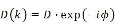
之一傅立葉變換運算(諸如(但不限於)一快速傅立葉變換(FFT))以產生一建構繞射平面影像:
Figure 02_image007
(1) 其中
Figure 02_image009
係振幅且
Figure 02_image011
係與樣本平面影像
Figure 02_image005
之傅立葉變換相關聯之相位。In one embodiment, the diffraction imaging algorithm 300 includes a step 302: taking a sample plane image
Figure 02_image005
Propagated to a diffraction plane to generate a constructed diffraction plane image. For example, step 302 may include performing a sample plane image
Figure 02_image005
A Fourier transform operation (such as, but not limited to, a Fast Fourier Transform (FFT)) to generate a constructed diffraction plane image:
Figure 02_image007
(1) of which
Figure 02_image009
is the amplitude and
Figure 02_image011
Department and sample planar image
Figure 02_image005
The phase associated with the Fourier transform of .

在另一實施例中,繞射成像演算法300包含一步驟304:將一繞射平面影像

Figure 02_image013
反向傳播至一樣本平面以產生一建構影像
Figure 02_image015
。例如,步驟304可包含執行一繞射平面影像
Figure 02_image017
之一傅立葉逆變換運算(諸如(但不限於)一快速傅立葉逆變換(IFFT))以形成一建構影像
Figure 02_image015
Figure 02_image019
(2)In another embodiment, the diffraction imaging algorithm 300 includes a step 304: taking a diffraction plane image
Figure 02_image013
Backpropagating to a sample plane to generate a constructed image
Figure 02_image015
. For example, step 304 may include performing a diffraction plane imaging
Figure 02_image017
an inverse Fourier transform operation (such as, but not limited to, an inverse fast Fourier transform (IFFT)) to form a constructed image
Figure 02_image015
:
Figure 02_image019
(2)

在另一實施例中,繞射成像演算法300包含一步驟306:應用有限支援以產生一經修改建構影像

Figure 02_image021
。例如,步驟306可包含根據值
Figure 02_image023
超出視域來將
Figure 02_image015
設定為零以產生一經修改建構影像
Figure 02_image021
。In another embodiment, the diffraction imaging algorithm 300 includes a step 306 of applying limited support to generate a modified constructed image
Figure 02_image021
. For example, step 306 may include according to the value
Figure 02_image023
out of sight
Figure 02_image015
Set to zero to produce a modified constructed image
Figure 02_image021
.

在另一實施例中,繞射成像演算法300包含一步驟308:執行經修改建構影像

Figure 02_image021
之一傅立葉變換以產生一經修改繞射影像
Figure 02_image025
Figure 02_image027
(3) 其中
Figure 02_image029
係振幅且
Figure 02_image031
Figure 02_image033
之相位。In another embodiment, the diffraction imaging algorithm 300 includes a step 308 of performing the modified image construction
Figure 02_image021
One Fourier transform to produce a modified diffraction image
Figure 02_image025
:
Figure 02_image027
(3) of which
Figure 02_image029
is the amplitude and
Figure 02_image031
Tie
Figure 02_image033
phase.

在另一實施例中,繞射成像演算法300包含一步驟310:用來自信號平面影像

Figure 02_image005
(例如來自步驟302)之相位資訊替換經修改繞射影像
Figure 02_image033
之相位之至少一部分。例如,步驟310可包含用
Figure 02_image011
之至少一部分替換
Figure 02_image035
之至少一部分。例如,可用來自
Figure 02_image011
之低頻資訊替換來自
Figure 02_image031
之低頻資訊。在此應認識到,與一成像系統相關聯之像差對相位
Figure 02_image011
之高頻部分之影響通常可大於對低頻部分之影響。因此,由
Figure 02_image011
之對應部分補充建構相位
Figure 02_image031
之至少低頻部分可促進一高解析度建構影像
Figure 02_image015
產生。In another embodiment, the diffraction imaging algorithm 300 includes a step 310: using the plane image from the signal
Figure 02_image005
Phase information (such as from step 302) replaces the modified diffraction image
Figure 02_image033
at least part of the phase. For example, step 310 may include using
Figure 02_image011
replace at least part of
Figure 02_image035
at least part of it. For example, available from
Figure 02_image011
The low-frequency information replacement comes from
Figure 02_image031
low-frequency information. It should be recognized here that the aberrations associated with an imaging system have a significant effect on the phase
Figure 02_image011
The influence of the high frequency part can usually be greater than the influence of the low frequency part. Therefore, by
Figure 02_image011
Complementary Constructive Aspects
Figure 02_image031
At least the low frequency portion of the
Figure 02_image015
produce.

在另一實施例中,繞射成像演算法300包含一步驟312:用來自繞射平面影像之振幅替換來自經修改繞射影像之振幅。例如,步驟312可包含用來自繞射平面影像

Figure 02_image013
之振幅
Figure 02_image037
替換經修改繞射影像之D' 。In another embodiment, the diffraction imaging algorithm 300 includes a step 312 of replacing the amplitude from the modified diffraction image with the amplitude from the diffraction plane image. For example, step 312 may include using the self-diffraction plane image
Figure 02_image013
Amplitude of
Figure 02_image037
Replace D' of the modified diffraction image.

在另一實施例中,繞射成像演算法300包含一步驟314:反覆步驟304至312,直至

Figure 02_image039
之值等於一選定容限內之
Figure 02_image037
之值。在另一實施例中,繞射成像演算法300包含一步驟316:提供經修改建構影像作為一輸出。因此,反覆相位恢復步驟可利用繞射平面影像之振幅
Figure 02_image037
及樣本平面影像之相位
Figure 02_image011
之至少部分兩者來產生具有比樣本平面影像高之解析度之一輸出影像
Figure 02_image015
(例如來自滿足終止條件之繞射成像演算法300之最後反覆之步驟304),儘管成像系統中存在像差。In another embodiment, the diffraction imaging algorithm 300 includes a step 314: repeat steps 304 to 312 until
Figure 02_image039
is equal to the value of the
Figure 02_image037
value. In another embodiment, the diffraction imaging algorithm 300 includes a step 316 of providing the modified constructed image as an output. Therefore, iterative phase recovery steps can exploit the amplitude of the diffraction plane image
Figure 02_image037
and the phase of the sample plane image
Figure 02_image011
at least some of both to produce an output image with a higher resolution than the sample planar image
Figure 02_image015
(eg, step 304 from the last iteration of the diffraction imaging algorithm 300 satisfying the termination condition), despite the presence of aberrations in the imaging system.

然而,在此應認識到,與圖3之相位恢復演算法相關聯之有限支援要求可能不適用於其中沿兩個或三個維度擴展一關注樣本之諸多檢測應用。It should be recognized here, however, that the limited support requirements associated with the phase recovery algorithm of FIG. 3 may not be suitable for many detection applications in which a sample of interest is expanded along two or three dimensions.

在另一實施例中,疊層技術用於將繞射成像技術(諸如(但不限於)圖3中所繪示之演算法)應用於適合於檢測系統之擴展樣本。例如,在一疊層技術中,針對多個樣本位置(例如成像區域)捕獲來自兩個或兩個以上部分之樣本平面影像及繞射平面影像兩者以形成一樣本之一擴展部分(例如大於一成像系統之一視域),其中樣本之相鄰部分(例如相鄰視域)之影像重疊。就此而言,兩個或兩個以上影像之各者之部分可用於成像演算法且重疊成像區域可補償任何給定成像區域中有限支援之缺乏。美國專利第10,162,161號之M.J. Humphry等人之「Ptychographic Electron Microscopy Using High-Angle Dark-Field Scattering for Sub-nanometer Resolution Imaging」(Nature Communications 3,730 (2012))及J.M. Rodenburg之「Ptychography and Related Diffractive Imaging Methods」(Advances in Imaging and Electron Physics 150,87-184 (2008))中大體上描述疊層成像技術,所有該等專利之全文以引用的方式併入本文中。In another embodiment, stacking techniques are used to apply diffractive imaging techniques, such as, but not limited to, the algorithm depicted in FIG. 3 , to extended samples suitable for detection systems. For example, in a stacking technique, both sample plane images and diffraction plane images from two or more portions are captured for multiple sample locations (e.g., imaging regions) to form an extended portion of a sample (e.g., larger than A field of view of an imaging system) in which images of adjacent portions of the sample (eg, adjacent fields of view) overlap. In this regard, portions of each of the two or more images can be used in the imaging algorithm and overlapping imaging regions can compensate for the lack of limited support in any given imaging region. "Ptychographic Electron Microscopy Using High-Angle Dark-Field Scattering for Sub-nanometer Resolution Imaging" by M.J. Humphry et al. of U.S. Patent No. 10,162,161 (Nature Communications 3, 730 (2012)) and "Ptychography and Related Diffractive Imaging" by J.M. Rodenburg Stacked imaging techniques are generally described in "Advances in Imaging and Electron Physics 150, 87-184 (2008)," the entire contents of which patents are incorporated herein by reference.

圖4係根據本發明之一或多個實施例之適合於疊層成像之一樣本上之一系列成像區域之一示意圖。在一實施例中,在各成像區域402處產生一樣本平面影像及一繞射平面影像。此外,可依任何選定分佈配置成像區域402,其中相鄰成像區域402至少部分重疊。例如圖4中所繪示,成像區域402可分佈成一陣列圖案以覆蓋樣本之一擴展區域。然而,應瞭解,圖4中所繪示之陣列圖案僅供說明且不應被解譯為限制。確切而言,可依任何選定分佈分佈成像區域402以形成具有任何大小或形狀之一擴展區域。4 is a schematic diagram of a series of imaging regions on a sample suitable for stack imaging according to one or more embodiments of the present invention. In one embodiment, a sample plane image and a diffraction plane image are generated at each imaging area 402 . Furthermore, imaging regions 402 may be configured in any selected distribution, wherein adjacent imaging regions 402 at least partially overlap. For example, as depicted in FIG. 4, the imaging regions 402 may be distributed in an array pattern to cover an extended area of the sample. It should be appreciated, however, that the array pattern depicted in FIG. 4 is for illustration only and should not be construed as limiting. Rather, imaging region 402 may be distributed in any selected distribution to form an extended region of any size or shape.

另外,各成像區域402可具有包含(但不限於)圓形(例如圖4中所繪示)、正方形或矩形之任何適合形狀。例如,各成像區域402之大小及形狀可對應於一成像系統(例如疊層檢測系統100)之一有效視域。因此,各成像區域402之大小及形狀可取決於及/或受限於系統之任何組件(其包含(但不限於)一偵測器或一孔隙)。Additionally, each imaging region 402 may have any suitable shape including, but not limited to, circular (such as depicted in FIG. 4 ), square, or rectangular. For example, the size and shape of each imaging area 402 may correspond to an effective field of view of an imaging system (eg, stack inspection system 100 ). Thus, the size and shape of each imaging region 402 may depend on and/or be limited by any component of the system including, but not limited to, a detector or an aperture.

圖5係繪示根據本發明之一或多個實施例之適合於使擴展樣本成像之一疊層成像技術500的一流程圖。然而,應瞭解,本文中所描述之疊層成像技術500僅供說明且不應被解譯為限制。確切而言,本發明之系統及方法可併入此項技術中已知之任何疊層成像技術,諸如(但不限於)一疊層反覆引擎(PIE)、增加型PIE (ePIE)或其類似者。FIG. 5 is a flowchart illustrating a stack imaging technique 500 suitable for imaging an extended sample in accordance with one or more embodiments of the present invention. However, it should be appreciated that the stacked imaging technique 500 described herein is for illustration only and should not be construed as limiting. Rather, the systems and methods of the present invention may be incorporated into any stack imaging technique known in the art, such as, but not limited to, a stack iteration engine (PIE), augmented PIE (ePIE), or the like .

在一實施例中,疊層成像技術500包含一步驟502:估計樣本之兩個或兩個以上選定部分(例如成像區域402)之一目標函數

Figure 02_image041
。例如,樣本之兩個或兩個以上成像區域402可表示為
Figure 02_image043
,其中
Figure 02_image045
係成像區域402之數目。In one embodiment, stack imaging technique 500 includes a step 502 of estimating an objective function for two or more selected portions of a sample (eg, imaging region 402 )
Figure 02_image041
. For example, two or more imaging regions 402 of a sample may be represented as
Figure 02_image043
,in
Figure 02_image045
is the number of imaging regions 402 .

在另一實施例中,疊層成像技術500包含一步驟504:估計具有一照明束之樣本之兩個或兩個以上成像區域402之一照明函數

Figure 02_image009
。例如,就圓形照明而言,照明函數可表示為:
Figure 02_image047
(4) 其中
Figure 02_image049
對應於一指數且
Figure 02_image051
對應於照明位置(例如成像區域402)之一陣列之第
Figure 02_image049
元素之位置處之照明函數,其中各照明元素具有一R半徑。In another embodiment, stack imaging technique 500 includes a step 504 of estimating an illumination function for two or more imaging regions 402 of a sample with an illumination beam
Figure 02_image009
. For example, for circular lighting, the lighting function can be expressed as:
Figure 02_image047
(4) of which
Figure 02_image049
corresponds to an exponent and
Figure 02_image051
The first of an array corresponding to an illumination location (eg, imaging area 402)
Figure 02_image049
The lighting function at the position of the element, where each lighting element has an R radius.

在另一實施例中,疊層成像技術500包含一步驟506:基於目標函數及照明函數來形成樣本之兩個或兩個以上成像區域402之一出射波函數。例如,一出射波函數可形成為:
Figure 02_image053
(5) 應注意,
Figure 02_image041
Figure 02_image009
兩者包含兩個或兩個以上成像區域
Figure 02_image043
。In another embodiment, the stack imaging technique 500 includes a step 506 of forming an outgoing wave function of two or more imaging regions 402 of the sample based on the objective function and the illumination function. For example, an outgoing wave function can be formed as:
Figure 02_image053
(5) It should be noted that
Figure 02_image041
and
Figure 02_image009
Both contain two or more imaging regions
Figure 02_image043
.

在另一實施例中,疊層成像技術500包含一步驟508:將出射波函數傳播至遠場以形成兩個或兩個以上成像區域402之一估計繞射圖案。例如,可使用一傅立葉變換運算(諸如(但不限於)一快速傅立葉變換運算)來將出射波函數傳播至遠場。In another embodiment, the stack imaging technique 500 includes a step 508 of propagating the outgoing wave function to the far field to form an estimated diffraction pattern for one of the two or more imaging regions 402 . For example, a Fourier transform operation such as, but not limited to, a fast Fourier transform operation may be used to propagate the outgoing wave function to the far field.

在另一實施例中,疊層成像技術500包含一步驟510:用來自與兩個或兩個以上成像區域402相關聯之信號平面影像之相位資訊替換估計繞射圖案之一相位之至少一部分。例如,可用來自各成像區域402之信號平面影像之低頻資訊替換來自估計繞射圖案之低頻資訊。如本文先前所描述,與一成像系統相關聯之像差對相位之高頻部分之影響通常可大於對低頻部分之影響。因此,由來自樣本平面影像之對應相位資訊補充估計繞射圖案之至少低頻部分可促進一高解析度輸出影像

Figure 02_image015
產生。In another embodiment, stack imaging technique 500 includes a step 510 of replacing at least a portion of a phase of the estimated diffraction pattern with phase information from signal plane images associated with two or more imaging regions 402 . For example, the low frequency information from the estimated diffraction pattern may be replaced by low frequency information from the signal planar image of each imaging region 402 . As previously described herein, aberrations associated with an imaging system can generally affect the high frequency portion of phase more than the low frequency portion. Therefore, supplementary estimation of at least the low frequency part of the diffraction pattern from the corresponding phase information from the sample plane image facilitates a high resolution output image
Figure 02_image015
produce.

在另一實施例中,疊層成像技術500包含一步驟512:用來自樣本之兩個或兩個以上成像區域402之繞射平面影像之振幅替換估計繞射圖案之一振幅以形成一更新估計繞射圖案。In another embodiment, stack imaging technique 500 includes a step 512 of replacing an amplitude of the estimated diffraction pattern with amplitudes of diffraction plane images from two or more imaging regions 402 of the sample to form an updated estimate Diffraction pattern.

在另一實施例中,疊層成像技術500包含一步驟514:反向傳播估計繞射圖案以形成一更新出射波函數

Figure 02_image055
。例如,可藉由使用一傅立葉逆變換運算(諸如(但不限於)一快速傅立葉逆變換運算)反向傳播估計繞射圖案來形成更新出射波函數。In another embodiment, stack imaging technique 500 includes a step 514 of backpropagating the estimated diffraction pattern to form an updated outgoing wave function
Figure 02_image055
. For example, the updated outgoing wave function may be formed by backpropagating the estimated diffraction pattern using an inverse Fourier transform operation such as, but not limited to, an inverse fast Fourier transform operation.

在另一實施例中,疊層成像技術500包含一步驟516:基於更新出射波函數來更新目標函數。例如,更新目標函數可特徵化為:

Figure 02_image057
(6)In another embodiment, the stack imaging technique 500 includes a step 516 of updating the objective function based on the updated outgoing wave function. For example, the update objective function can be characterized as:
Figure 02_image057
(6)

在另一實施例中,疊層成像技術500包含一步驟518:反覆步驟506至516,直至兩個連續估計出射波函數之間的差(例如

Figure 02_image059
)低於一選定收斂臨限值。在另一實施例中,疊層成像技術500包含一步驟520:提供更新目標函數作為一輸出。就此而言,基於輸出目標函數之建構樣本平面影像可具有高於一直接產生之樣本平面影像之一解析度。In another embodiment, stack imaging technique 500 includes a step 518 of repeating steps 506 to 516 until the difference between two consecutive estimated outgoing wave functions (e.g.
Figure 02_image059
) below a chosen convergence threshold. In another embodiment, the stack imaging technique 500 includes a step 520 of providing an updated objective function as an output. In this regard, the constructed sample plane image based on the output objective function may have a higher resolution than a directly generated sample plane image.

此外,在此應認識到,相鄰影像(例如樣本平面影像及/或繞射平面影像)之間的重疊度可影響疊層成像技術500之通量之敏感度及/或效率。例如,增加相鄰成像區域之間的重疊可減少收斂所需之反覆數。然而,增加相鄰成像區域之間的重疊會因需要捕獲更多影像來特徵化樣本上之一選定區域而負面影響總通量。因此,可調整連續成像區域之間的重疊度(例如與樣本平面及/或繞射平面影像相關聯)以提供疊層成像技術500之通量與敏感度之間的一選定平衡。Furthermore, it should be recognized herein that the degree of overlap between adjacent images (eg, sample plane images and/or diffraction plane images) can affect the sensitivity and/or efficiency of the throughput of stack imaging technique 500 . For example, increasing the overlap between adjacent imaged regions can reduce the number of iterations required for convergence. However, increasing the overlap between adjacent imaged regions can negatively impact overall throughput by requiring more images to be captured to characterize a selected region on the sample. Thus, the degree of overlap between consecutive imaged regions (eg, associated with sample plane and/or diffraction plane images) can be adjusted to provide a selected balance between throughput and sensitivity of stack imaging technique 500 .

本文中所描述之標的有時繪示含於其他組件內或與其他組件連接之不同組件。應瞭解,此等描繪架構僅供例示,且事實上,可實施達成相同功能之諸多其他架構。就概念而言,用於達成相同功能之組件之任何配置經有效「相關聯」以達成所要功能。因此,本文中經組合以達成一特定功能之任何兩個組件可被視為彼此「相關聯」以達成所要功能,不管架構或中間組件如何。同樣地,如此相關聯之任何兩個組件亦可被視為彼此「連接」或「耦合」以達成所要功能,且能夠如此相關聯之任何兩個組件亦可被視為彼此「可耦合」以達成所要功能。「可耦合」之具體實例包含(但不限於)可實體互動及/或實體互動組件、及/或可無線互動及/或無線互動組件及/或可邏輯互動及/或邏輯互動組件。The subject matter described herein sometimes depicts different components contained within, or connected with, other components. It is to be understood that these depicted architectures are illustrative only, and that in fact many other architectures can be implemented which achieve the same functionality. Conceptually, any arrangement of components to achieve the same functionality is effectively "associated" to achieve the desired functionality. Hence, any two components herein combined to achieve a particular functionality can be seen as "associated with" each other to achieve the desired functionality, regardless of architectures or intermediary components. Likewise, any two components so associated can also be considered to be "connected" or "coupled" to each other for a desired functionality, and any two components capable of being so associated can also be considered to be "coupleable" to each other for the purpose of achieve the desired function. Specific examples of "couplable" include, but are not limited to, physically interactable and/or physically interactable components, and/or wirelessly interactable and/or wirelessly interactable components, and/or logically interactable and/or logically interactable components.

據信,可藉由以上描述來理解本發明及其諸多伴隨優點,且應明白,可在不背離本發明或不犧牲其所有材料優點之情況下對組件之形式、建構及配置作出各種改變。所描述之形式僅供說明,且以下申請專利範圍意欲涵蓋及包含此等改變。此外,應瞭解,本發明由隨附申請專利範圍界定。It is believed that the present invention and its many attendant advantages can be understood from the foregoing description, and it should be understood that various changes in form, construction and arrangement of components may be made without departing from the invention or sacrificing all of its material advantages. The forms described are for illustration only and such variations are intended to be covered and encompassed by the following claims. Furthermore, it should be understood that the present invention is defined by the claims of the appended applications.

100:疊層檢測系統 102:投影成像子系統 104:控制器 106:處理器 108:記憶體媒體 110:粒子源 112:照明束 114:樣本 116:物鏡 118:照明光學器件 120:投影光學器件 122:樣本輻射 124:偵測器 126:磁稜鏡 128:孔隙 130:樣本平面 132:繞射平面 200:檢測方法 202:步驟 204:步驟 206:步驟 300:繞射成像演算法 302:步驟 304:步驟 306:步驟 308:步驟 310:步驟 312:步驟 314:步驟 316:步驟 402:成像區域 500:疊層成像技術 502:步驟 504:步驟 506:步驟 508:步驟 510:步驟 512:步驟 514:步驟 516:步驟 518:步驟 520:步驟100: Lamination inspection system 102:Projection imaging subsystem 104: Controller 106: Processor 108:Memory media 110: Particle source 112: lighting beam 114: sample 116: objective lens 118: Illumination Optics 120: Projection optics 122: Sample Radiation 124: Detector 126: Magnet 128: porosity 130: sample plane 132: Diffraction plane 200: Detection method 202: Step 204: step 206: Step 300: Diffraction Imaging Algorithm 302: Step 304: step 306: Step 308: Step 310: step 312: Step 314: Step 316: Step 402: Imaging area 500: Stack Imaging Technology 502: Step 504: step 506: Step 508: Step 510: step 512: Step 514: step 516: step 518:Step 520: step

熟習技術者可藉由參考附圖來較佳理解本發明之諸多優點,其中: 圖1A係根據本發明之一或多個實施例之適合於使用粒子束之反射模式成像之一疊層檢測系統之一方塊圖; 圖1B係根據本發明之一或多個實施例之一投影成像子系統之一概念圖; 圖2係繪示根據本發明之一或多個實施例之一檢測方法中所執行之步驟的一流程圖; 圖3係繪示根據本發明之一或多個實施例之用於自樣本之一共同部分之一繞射平面影像及一樣本平面影像產生一高解析度輸出影像之一反覆繞射成像演算法的一流程圖; 圖4係根據本發明之一或多個實施例之適合於疊層成像之一樣本上之一系列成像區域之一示意圖;及 圖5係繪示根據本發明之一或多個實施例之適合於成像擴展樣本之一疊層成像技術的一流程圖。Those skilled in the art can better understand many advantages of the present invention by referring to the accompanying drawings, in which: Figure 1A is a block diagram of an overlay inspection system suitable for reflection mode imaging using a particle beam in accordance with one or more embodiments of the present invention; FIG. 1B is a conceptual diagram of a projection imaging subsystem according to one or more embodiments of the present invention; FIG. 2 is a flowchart illustrating the steps performed in a detection method according to one or more embodiments of the present invention; Figure 3 illustrates an iterative diffraction imaging algorithm for generating a high resolution output image from a diffraction plane image of a common portion of a sample and a sample plane image in accordance with one or more embodiments of the present invention a flowchart of Figure 4 is a schematic diagram of a series of imaging regions on a sample suitable for stack imaging according to one or more embodiments of the present invention; and 5 is a flowchart illustrating a stack imaging technique suitable for imaging an extended sample, according to one or more embodiments of the present invention.

100:疊層檢測系統 100: Lamination inspection system

102:投影成像子系統 102:Projection imaging subsystem

104:控制器 104: Controller

106:處理器 106: Processor

108:記憶體媒體 108:Memory media

110:粒子源 110: Particle source

112:照明束 112: lighting beam

114:樣本 114: sample

116:物鏡 116: objective lens

118:照明光學器件 118: Illumination Optics

120:投影光學器件 120: Projection optics

122:樣本輻射 122: Sample Radiation

124:偵測器 124: Detector

126:磁稜鏡 126: Magnet

128:孔隙 128: porosity

130:樣本平面 130: sample plane

132:繞射平面 132: Diffraction plane

Claims (32)

一種粒子束檢測系統,其包括:一反射粒子束成像系統,其提供一樣本之一選定部分之一影像及該樣本之該選定部分之一繞射圖案;及一控制器,其通信耦合至該反射粒子束成像系統,該控制器包含經組態以執行程式指令之一或多個處理器,該等程式指令引起該一或多個處理器:自該反射粒子束成像系統接收與該樣本之兩個或兩個以上選定部分相關聯之兩個或兩個以上樣本平面影像,其中該樣本之該兩個或兩個以上選定部分之至少若干者重疊;自該反射粒子束成像系統接收與該樣本之該兩個或兩個以上選定部分相關聯之兩個或兩個以上繞射平面影像;及使用自該兩個或兩個以上樣本平面影像獲得之相位資訊來使該樣本之該兩個或兩個以上選定部分之一或多個輸出影像由該兩個或兩個以上繞射平面影像建構。 A particle beam detection system comprising: a reflective particle beam imaging system providing an image of a selected portion of a sample and a diffraction pattern of the selected portion of the sample; and a controller communicatively coupled to the Reflective particle beam imaging system, the controller including one or more processors configured to execute programmed instructions that cause the one or more processors to: two or more sample planar images associated with two or more selected portions, wherein at least some of the two or more selected portions of the sample overlap; two or more diffraction plane images associated with the two or more selected portions of the sample; and using phase information obtained from the two or more sample plane images to make the two or more diffraction plane images of the sample Or one or more output images of two or more selected parts are constructed from the two or more diffraction plane images. 如請求項1之粒子束檢測系統,其中該一或多個輸出影像具有比與該樣本之該兩個或兩個以上選定部分相關聯之該兩個或兩個以上樣本平面影像及該兩個或兩個以上繞射平面影像高之解析度。 The particle beam detection system of claim 1, wherein the one or more output images have a ratio of the two or more sample plane images associated with the two or more selected portions of the sample and the two Or more than two diffraction plane images with high resolution. 如請求項1之粒子束檢測系統,其中該一或多個處理器經組態以藉由以下操作來使用自該兩個或兩個以上樣本平面影像獲得之相位資訊來使該 樣本之該兩個或兩個以上選定部分之一或多個輸出影像由該兩個或兩個以上繞射平面影像建構:基於一疊層成像技術,使用自該兩個或兩個以上樣本平面影像獲得之相位資訊來使該樣本之該兩個或兩個以上選定部分之一或多個輸出影像由該兩個或兩個以上繞射平面影像建構。 The particle beam detection system of claim 1, wherein the one or more processors are configured to use phase information obtained from the two or more sample plane images to make the One or more output images of the two or more selected portions of the sample are constructed from the two or more diffraction plane images: based on a stacked imaging technique, using images from the two or more sample planes Image-derived phase information is used to construct one or more output images of the two or more selected portions of the sample from the two or more diffraction plane images. 如請求項3之粒子束檢測系統,其中該一或多個處理器經組態以藉由以下操作來執行該疊層成像技術:估計該樣本之該兩個或兩個以上選定部分之一目標函數;估計具有一照明束之該樣本之該兩個或兩個以上選定部分之一照明函數;基於該目標函數及該照明函數來形成該樣本之該兩個或兩個以上選定部分之一出射波函數;將該出射波函數傳播至遠場以形成一估計繞射圖案;用來自與該樣本之該兩個或兩個以上選定部分相關聯之該兩個或兩個以上樣本平面影像之相位資訊替換該估計繞射圖案之一相位;用與該樣本之該兩個或兩個以上選定部分相關聯之該兩個或兩個以上繞射平面影像替換該估計繞射圖案之一模數;反向傳播該估計繞射圖案以形成一更新出射波函數;基於該更新出射波函數來更新該目標函數;及基於該更新目標函數來提供一輸出影像。 The particle beam detection system of claim 3, wherein the one or more processors are configured to perform the stack imaging technique by: estimating a target of one of the two or more selected portions of the sample function; estimating an illumination function of the two or more selected portions of the sample with an illumination beam; forming an exit of the two or more selected portions of the sample based on the objective function and the illumination function wave function; propagating the outgoing wave function to the far field to form an estimated diffraction pattern; using phases from the two or more sample plane images associated with the two or more selected portions of the sample replacing a phase of the estimated diffraction pattern with information; replacing a modulus of the estimated diffraction pattern with images of the two or more diffraction planes associated with the two or more selected portions of the sample; backpropagating the estimated diffraction pattern to form an updated outgoing wave function; updating the objective function based on the updated outgoing wave function; and providing an output image based on the updated objective function. 如請求項4之粒子束檢測系統,其進一步包括: 反覆以下步驟:將該出射波函數傳播至遠場以形成一估計繞射圖案;用來自與該樣本之該兩個或兩個以上選定部分相關聯之該兩個或兩個以上樣本平面影像之相位資訊替換該估計繞射圖案之一相位;用與該樣本之該兩個或兩個以上選定部分相關聯之該兩個或兩個以上繞射平面影像替換該估計繞射圖案之一模數;反向傳播該估計繞射圖案以形成一更新出射波函數;及基於該更新出射波函數來更新該目標函數,直至兩個連續估計出射波函數之間的一差低於一選定收斂臨限值,其中該輸出影像係基於該更新目標函數提供低於該選定收斂臨限值之兩個連續估計出射波函數之間的該差。 As the particle beam detection system of claim 4, it further includes: Iterating the steps of: propagating the outgoing wave function to the far field to form an estimated diffraction pattern; using data from the two or more sample plane images associated with the two or more selected portions of the sample replacing a phase of the estimated diffraction pattern with phase information; replacing a modulus of the estimated diffraction pattern with images of the two or more diffraction planes associated with the two or more selected portions of the sample ; backpropagating the estimated diffraction pattern to form an updated outgoing wave function; and updating the objective function based on the updated outgoing wave function until a difference between two consecutive estimated outgoing wave functions is below a selected convergence threshold value, wherein the output image is based on the updated objective function providing the difference between two successive estimated outgoing wave functions below the selected convergence threshold. 如請求項1之粒子束檢測系統,其中該反射粒子束成像系統包括:一反射電子束成像系統。 The particle beam detection system according to claim 1, wherein the reflected particle beam imaging system comprises: a reflected electron beam imaging system. 如請求項6之粒子束檢測系統,其中與該樣本之該兩個或兩個以上選定部分相關聯之該兩個或兩個以上樣本平面影像包括:低能電子顯微鏡影像。 The particle beam detection system according to claim 6, wherein the two or more sample plane images associated with the two or more selected portions of the sample include: low-energy electron microscope images. 如請求項6之粒子束檢測系統,其中該反射電子束成像系統包括:一電子源,其經組態以產生一電子束;一物鏡;一磁稜鏡,其導引該電子束至該物鏡,其中該物鏡使用該電子束來 照射一樣本之選定部分,其中該物鏡自該樣本之該選定部分收集發射電子;一或多個電子偵測器;及一或多個投影透鏡,其中該磁稜鏡導引由該物鏡收集之該等發射電子至該一或多個投影透鏡,其中該一或多個投影透鏡將該兩個或兩個以上樣本平面影像提供於該一或多個電子偵測器之至少一者上且將該兩個或兩個以上繞射平面影像提供於該一或多個電子偵測器之至少一者上。 The particle beam detection system as claimed in claim 6, wherein the reflected electron beam imaging system includes: an electron source configured to generate an electron beam; an objective lens; a magnet that guides the electron beam to the objective lens , where the objective uses the electron beam to illuminating a selected portion of a sample, wherein the objective lens collects emitted electrons from the selected portion of the sample; one or more electron detectors; and one or more projection lenses, wherein the magnetite guides electrons collected by the objective lens The electrons are emitted to the one or more projection lenses, wherein the one or more projection lenses provide the two or more sample plane images on at least one of the one or more electron detectors and will The two or more diffraction plane images are provided on at least one of the one or more electronic detectors. 如請求項8之粒子束檢測系統,其中該一或多個電子偵測器包括:一單一電子偵測器,其中該一或多個投影透鏡循序提供:該單一電子偵測器上之一選定樣本位置之該兩個或兩個以上樣本平面影像之一者;及至該單一電子偵測器之該樣本之該選定部分之該兩個或兩個以上繞射平面影像之一者。 The particle beam detection system of claim 8, wherein the one or more electron detectors include: a single electron detector, wherein the one or more projection lenses sequentially provide: a selected one on the single electron detector one of the two or more sample plane images of the sample location; and one of the two or more diffraction plane images of the selected portion of the sample to the single electron detector. 如請求項9之粒子束檢測系統,其進一步包括:一或多個平移台,其等選擇性定位該一或多個投影透鏡之至少一者。 The particle beam detection system according to claim 9, further comprising: one or more translation stages, which selectively position at least one of the one or more projection lenses. 如請求項9之粒子束檢測系統,其中該一或多個投影透鏡之至少一者具有一可選聚焦力。 The particle beam detection system according to claim 9, wherein at least one of the one or more projection lenses has a selectable focusing power. 如請求項7之粒子束檢測系統,其中該反射粒子束成像系統中之該樣 本上之一電子束之一著陸能可調。 The particle beam detection system as claimed in item 7, wherein the sample in the reflected particle beam imaging system The landing energy of one of the electron beams is adjustable. 如請求項1之粒子束檢測系統,其中該兩個或兩個以上選定部分之至少若干者之間的該重疊可調。 The particle beam detection system of claim 1, wherein the overlap between at least some of the two or more selected portions is adjustable. 如請求項1之粒子束檢測系統,其中該反射粒子束成像系統包括:一反射離子束成像系統。 The particle beam detection system according to claim 1, wherein the reflected particle beam imaging system comprises: a reflected ion beam imaging system. 一種粒子束檢測系統,其包括:一控制器,其通信耦合至一反射粒子束成像系統,該反射粒子束成像系統提供一樣本之一選定部分之一影像及該樣本之該選定部分之一繞射圖案,該控制器包含經組態以執行程式指令之一或多個處理器,該等程式指令引起該一或多個處理器:自該反射粒子束成像系統接收與該樣本之兩個或兩個以上選定部分相關聯之兩個或兩個以上樣本平面影像,其中該樣本之該兩個或兩個以上選定部分之至少若干者重疊;自該反射粒子束成像系統接收與該樣本之該兩個或兩個以上選定部分相關聯之兩個或兩個以上繞射平面影像;及使用自該兩個或兩個以上樣本平面影像獲得之相位資訊來使該樣本之該兩個或兩個以上選定部分之一或多個輸出影像由該兩個或兩個以上繞射平面影像建構。 A particle beam detection system comprising: a controller communicatively coupled to a reflective particle beam imaging system that provides an image of a selected portion of a sample and a surrounding area of the selected portion of the sample The controller includes one or more processors configured to execute programmed instructions that cause the one or more processors to: receive from the reflected particle beam imaging system two or more Two or more sample planar images associated with two or more selected portions, wherein at least some of the two or more selected portions of the sample overlap; two or more diffraction plane images associated with two or more selected portions; and using phase information obtained from the two or more sample plane images to make the two or more samples of the sample One or more output images of the above selected portion are constructed from the two or more diffraction plane images. 如請求項15之粒子束檢測系統,其中該一或多個輸出影像具有比與 該樣本之該兩個或兩個以上選定部分相關聯之該兩個或兩個以上樣本平面影像及該兩個或兩個以上繞射平面影像高之解析度。 The particle beam detection system as claimed in claim 15, wherein the one or more output images have a ratio and Resolution of the two or more sample plane images and the two or more diffraction plane images associated with the two or more selected portions of the sample. 如請求項15之粒子束檢測系統,其中該一或多個處理器經組態以藉由以下操作來使用自該兩個或兩個以上樣本平面影像獲得之相位資訊來使該樣本之該兩個或兩個以上選定部分之一或多個輸出影像由該兩個或兩個以上繞射平面影像建構:基於一疊層成像技術,使用自該兩個或兩個以上樣本平面影像獲得之相位資訊來使該樣本之該兩個或兩個以上選定部分之一或多個輸出影像由該兩個或兩個以上繞射平面影像建構。 The particle beam detection system of claim 15, wherein the one or more processors are configured to use phase information obtained from the two or more sample plane images to make the two of the sample One or more output images of one or more selected parts are constructed from the two or more diffractive planar images: based on a stack imaging technique using phases obtained from the two or more sample planar images information such that one or more output images of the two or more selected portions of the sample are constructed from the two or more diffraction plane images. 如請求項17之粒子束檢測系統,其中該一或多個處理器經組態以藉由以下操作來執行該疊層成像技術:估計該樣本之該兩個或兩個以上選定部分之一目標函數;估計具有一照明束之該樣本之該兩個或兩個以上選定部分之一照明函數;基於該目標函數及該照明函數來形成該樣本之該兩個或兩個以上選定部分之一出射波函數;將該出射波函數傳播至遠場以形成一估計繞射圖案;用來自與該樣本之該兩個或兩個以上選定部分相關聯之該兩個或兩個以上樣本平面影像之相位資訊替換該估計繞射圖案之一相位;用與該樣本之該兩個或兩個以上選定部分相關聯之該兩個或兩個以上繞射平面影像替換該估計繞射圖案之一模數; 反向傳播該估計繞射圖案以形成一更新出射波函數;基於該更新出射波函數來更新該目標函數;及基於該更新目標函數來提供一輸出影像。 The particle beam detection system of claim 17, wherein the one or more processors are configured to perform the stack imaging technique by: estimating a target of one of the two or more selected portions of the sample function; estimating an illumination function of the two or more selected portions of the sample with an illumination beam; forming an exit of the two or more selected portions of the sample based on the objective function and the illumination function wave function; propagating the outgoing wave function to the far field to form an estimated diffraction pattern; using phases from the two or more sample plane images associated with the two or more selected portions of the sample replacing a phase of the estimated diffraction pattern with information; replacing a modulus of the estimated diffraction pattern with images of the two or more diffraction planes associated with the two or more selected portions of the sample; backpropagating the estimated diffraction pattern to form an updated outgoing wave function; updating the objective function based on the updated outgoing wave function; and providing an output image based on the updated objective function. 如請求項18之粒子束檢測系統,其中基於該更新出射波函數來更新該目標函數包括:反覆以下步驟:將該出射波函數傳播至遠場以形成一估計繞射圖案;用來自與該樣本之該兩個或兩個以上選定部分相關聯之該兩個或兩個以上樣本平面影像之相位資訊替換該估計繞射圖案之一相位;用與該樣本之該兩個或兩個以上選定部分相關聯之該兩個或兩個以上繞射平面影像替換該估計繞射圖案之一模數;反向傳播該估計繞射圖案以形成一更新出射波函數;及基於該更新出射波函數來更新該目標函數,直至兩個連續估計出射波函數之間的一差低於一選定收斂臨限值,其中該輸出影像係基於該更新目標函數提供低於該選定收斂臨限值之兩個連續估計出射波函數之間的該差。 The particle beam detection system of claim 18, wherein updating the objective function based on the updated outgoing wave function comprises: repeating the steps of: propagating the outgoing wave function to the far field to form an estimated diffraction pattern; Replace a phase of the estimated diffraction pattern with phase information of the two or more sample plane images associated with the two or more selected portions of the sample; replacing a modulus of the estimated diffraction pattern by associating the two or more diffraction plane images; backpropagating the estimated diffraction pattern to form an updated outgoing wave function; and updating based on the updated outgoing wave function the objective function until a difference between two successive estimates of the outgoing wave function falls below a selected convergence threshold, wherein the output image is based on the updated objective function providing two successive estimates below the selected convergence threshold This difference between the outgoing wave functions. 如請求項15之粒子束檢測系統,其中該反射粒子束成像系統包括:一反射電子束成像系統。 The particle beam detection system according to claim 15, wherein the reflected particle beam imaging system comprises: a reflected electron beam imaging system. 如請求項20之粒子束檢測系統,其中與該樣本之該兩個或兩個以上選定部分相關聯之該兩個或兩個以上樣本平面影像包括: 低能電子顯微鏡影像。 The particle beam detection system according to claim 20, wherein the two or more sample plane images associated with the two or more selected portions of the sample include: Low-energy electron microscope image. 如請求項20之粒子束檢測系統,其中該反射電子束成像系統包括:一電子源,其經組態以產生一電子束;一物鏡;一磁稜鏡,其導引該電子束至該物鏡,其中該物鏡使用該電子束來照射一樣本之選定部分,其中該物鏡自該樣本之該選定部分收集發射電子;一或多個電子偵測器;及一或多個投影透鏡,其中該磁稜鏡導引由該物鏡收集之該等發射電子至該一或多個投影透鏡,其中該一或多個投影透鏡將該兩個或兩個以上樣本平面影像提供於該一或多個電子偵測器之至少一者上且將該兩個或兩個以上繞射平面影像提供於該一或多個電子偵測器之至少一者上。 The particle beam detection system of claim 20, wherein the reflected electron beam imaging system includes: an electron source configured to generate an electron beam; an objective lens; a magnet that guides the electron beam to the objective lens , wherein the objective lens uses the electron beam to illuminate a selected portion of a sample, wherein the objective lens collects emitted electrons from the selected portion of the sample; one or more electron detectors; and one or more projection lenses, wherein the magnetic guiding the emitted electrons collected by the objective lens to the one or more projection lenses, wherein the one or more projection lenses provide the two or more sample plane images to the one or more electron detectors on at least one of the electronic detectors and provide the two or more diffraction plane images on at least one of the one or more electronic detectors. 如請求項22之粒子束檢測系統,其中該一或多個電子偵測器包括:一單一電子偵測器,其中該一或多個投影透鏡循序提供:該單一電子偵測器上之一選定樣本位置之該兩個或兩個以上樣本平面影像之一者;及至該單一電子偵測器之該樣本之該選定部分之該兩個或兩個以上繞射平面影像之一者。 The particle beam detection system of claim 22, wherein the one or more electron detectors include: a single electron detector, wherein the one or more projection lenses sequentially provide: a selected one on the single electron detector one of the two or more sample plane images of the sample location; and one of the two or more diffraction plane images of the selected portion of the sample to the single electron detector. 如請求項23之粒子束檢測系統,其進一步包括:一或多個平移台,其等選擇性定位該一或多個投影透鏡之至少一 者。 The particle beam detection system of claim 23, further comprising: one or more translation stages, which selectively position at least one of the one or more projection lenses By. 如請求項23之粒子束檢測系統,其中該一或多個投影透鏡之至少一者具有一可選聚焦力。 The particle beam detection system according to claim 23, wherein at least one of the one or more projection lenses has a selectable focusing power. 如請求項21之粒子束檢測系統,其中該反射粒子束成像系統中之該樣本上之一電子束之一著陸能可調。 The particle beam detection system according to claim 21, wherein a landing energy of an electron beam on the sample in the reflected particle beam imaging system is adjustable. 如請求項15之粒子束檢測系統,其中該兩個或兩個以上選定部分之至少若干者之間的該重疊可調。 The particle beam detection system of claim 15, wherein the overlap between at least some of the two or more selected portions is adjustable. 如請求項15之粒子束檢測系統,其中該反射粒子束成像系統包括:一反射離子束成像系統。 The particle beam detection system according to claim 15, wherein the reflected particle beam imaging system includes: a reflected ion beam imaging system. 一種檢測方法,其包括:自一反射粒子束成像系統接收與樣本之兩個或兩個以上選定部分相關聯之兩個或兩個以上樣本平面影像,其中該樣本之該兩個或兩個以上選定部分之至少若干者重疊;自該反射粒子束成像系統接收與該樣本之該兩個或兩個以上選定部分相關聯之兩個或兩個以上繞射平面影像;及使用自該兩個或兩個以上樣本平面影像獲得之相位資訊來使該樣本之該兩個或兩個以上選定部分之一或多個輸出影像由該兩個或兩個以上繞射平面影像建構。 A detection method comprising: receiving two or more sample plane images associated with two or more selected portions of a sample from a reflected particle beam imaging system, wherein the two or more at least some of the selected portions overlap; receiving from the reflected particle beam imaging system two or more diffraction plane images associated with the two or more selected portions of the sample; Phase information obtained from two or more sample plane images is used to construct one or more output images of the two or more selected portions of the sample from the two or more diffraction plane images. 如請求項29之方法,其中使用自該兩個或兩個以上樣本平面影像獲得之相位資訊來使該樣本之該兩個或兩個以上選定部分之一或多個輸出影像由該兩個或兩個以上繞射平面影像建構包括:基於一疊層成像技術,使用自該兩個或兩個以上樣本平面影像獲得之相位資訊來使該樣本之該兩個或兩個以上選定部分之一或多個輸出影像由兩個或兩個以上繞射平面影像建構。 The method of claim 29, wherein phase information obtained from the two or more sample plane images is used to cause one or more output images of the two or more selected portions of the sample to be generated by the two or more The construction of two or more diffraction planar images includes: using phase information obtained from the two or more sample planar images to make one or more of the two or more selected portions of the sample based on a stack imaging technique. Multiple output images are constructed from two or more diffraction plane images. 如請求項30之方法,其中基於一疊層成像技術使用自該兩個或兩個以上樣本平面影像獲得之相位資訊來使該樣本之該兩個或兩個以上選定部分之一或多個輸出影像由該兩個或兩個以上繞射平面影像建構包括:估計該樣本之該兩個或兩個以上選定部分之一目標函數;估計具有一照明束之該樣本之該兩個或兩個以上選定部分之一照明函數;基於該目標函數及該照明函數來形成該樣本之該兩個或兩個以上選定部分之一出射波函數;將該出射波函數傳播至遠場以形成一估計繞射圖案;用來自與該樣本之該兩個或兩個以上選定部分相關聯之該兩個或兩個以上樣本平面影像之相位資訊替換該估計繞射圖案之一相位;用與該樣本之該兩個或兩個以上選定部分相關聯之該兩個或兩個以上繞射平面影像替換該估計繞射圖案之一模數;反向傳播該估計繞射圖案以形成一更新出射波函數;基於該更新出射波函數來更新該目標函數;及 基於該更新目標函數來提供一輸出影像。 The method of claim 30, wherein one or more of the two or more selected portions of the sample are output using phase information obtained from the two or more sample plane images based on a stack imaging technique Image construction from the two or more diffractive plane images includes: estimating an objective function of the two or more selected portions of the sample; estimating the two or more of the sample with an illumination beam an illumination function of selected portions; forming an outgoing wave function of the two or more selected portions of the sample based on the objective function and the illuminating function; propagating the outgoing wave function to the far field to form an estimated diffraction pattern; replacing a phase of the estimated diffraction pattern with phase information from the two or more sample plane images associated with the two or more selected portions of the sample; The two or more diffraction plane images associated with one or more selected portions replace a modulus of the estimated diffraction pattern; backpropagating the estimated diffraction pattern to form an updated outgoing wave function; based on the updating the outgoing wave function to update the objective function; and An output image is provided based on the update objective function. 如請求項31之方法,其進一步包括:反覆以下步驟:將該出射波函數傳播至遠場以形成一估計繞射圖案;用來自與該樣本之該兩個或兩個以上選定部分相關聯之該兩個或兩個以上樣本平面影像之相位資訊替換該估計繞射圖案之一相位;用與該樣本之該兩個或兩個以上選定部分相關聯之該兩個或兩個以上繞射平面影像替換該估計繞射圖案之一模數;反向傳播該估計繞射圖案以形成一更新出射波函數;及基於該更新出射波函數來更新該目標函數,直至兩個連續估計出射波函數之間的一差低於一選定收斂臨限值,其中該輸出影像係基於該更新目標函數提供低於該選定收斂臨限值之兩個連續估計出射波函數之間的該差。 The method of claim 31, further comprising: repeating the steps of: propagating the outgoing wave function to the far field to form an estimated diffraction pattern; replacing a phase of the estimated diffraction pattern with phase information of the two or more sample plane images; using the two or more diffraction planes associated with the two or more selected portions of the sample image replacing a modulus of the estimated diffraction pattern; backpropagating the estimated diffraction pattern to form an updated outgoing wave function; and updating the objective function based on the updated outgoing wave function until two consecutive estimated outgoing wave functions A difference between two successive estimated outgoing wave functions below a selected convergence threshold, wherein the output image is based on the updated objective function providing the difference between two successively estimated outgoing wave functions below the selected convergence threshold.
TW108117595A 2018-05-23 2019-05-22 Reflection-mode electron-beam inspection using ptychographic imaging TWI788570B (en)

Applications Claiming Priority (4)

Application Number Priority Date Filing Date Title
US201862675645P 2018-05-23 2018-05-23
US62/675,645 2018-05-23
US16/412,505 US10755892B2 (en) 2018-05-23 2019-05-15 Reflection-mode electron-beam inspection using ptychographic imaging
US16/412,505 2019-05-15

Publications (2)

Publication Number Publication Date
TW202012922A TW202012922A (en) 2020-04-01
TWI788570B true TWI788570B (en) 2023-01-01

Family

ID=68614053

Family Applications (1)

Application Number Title Priority Date Filing Date
TW108117595A TWI788570B (en) 2018-05-23 2019-05-22 Reflection-mode electron-beam inspection using ptychographic imaging

Country Status (3)

Country Link
US (1) US10755892B2 (en)
TW (1) TWI788570B (en)
WO (1) WO2019226578A1 (en)

Families Citing this family (3)

* Cited by examiner, † Cited by third party
Publication number Priority date Publication date Assignee Title
FR3110026B1 (en) * 2020-05-05 2022-06-10 Commissariat Energie Atomique Pulsed source of electrons and surface analysis system comprising such a pulsed source
CN116385578A (en) * 2023-03-06 2023-07-04 中国科学院上海光学精密机械研究所 Single Pixel Diffraction Imaging Method
EP4575645A1 (en) * 2023-12-20 2025-06-25 ASML Netherlands B.V. Leed and ptychography based surface profile determination

Citations (3)

* Cited by examiner, † Cited by third party
Publication number Priority date Publication date Assignee Title
US20160266366A1 (en) * 2015-03-13 2016-09-15 California Institute Of Technology Correcting for aberrations in incoherent imaging systems using fourier ptychographic techniques
US20170031246A1 (en) * 2015-07-30 2017-02-02 Asml Netherlands B.V. Inspection Apparatus, Inspection Method and Manufacturing Method
US20180048811A1 (en) * 2015-01-29 2018-02-15 The Regents Of The University Of California Patterned-illumination systems adopting a computational illumination

Family Cites Families (5)

* Cited by examiner, † Cited by third party
Publication number Priority date Publication date Assignee Title
US7348566B2 (en) 2006-02-28 2008-03-25 International Business Machines Corporation Aberration-correcting cathode lens microscopy instrument
EP2690648B1 (en) 2012-07-26 2014-10-15 Fei Company Method of preparing and imaging a lamella in a particle-optical apparatus
GB201215558D0 (en) * 2012-08-31 2012-10-17 Phase Focus Ltd Improvements in phase retrieval
US10162161B2 (en) 2014-05-13 2018-12-25 California Institute Of Technology Ptychography imaging systems and methods with convex relaxation
EP3106862B1 (en) * 2015-06-18 2019-01-16 FEI Company Method of ptychographic imaging

Patent Citations (3)

* Cited by examiner, † Cited by third party
Publication number Priority date Publication date Assignee Title
US20180048811A1 (en) * 2015-01-29 2018-02-15 The Regents Of The University Of California Patterned-illumination systems adopting a computational illumination
US20160266366A1 (en) * 2015-03-13 2016-09-15 California Institute Of Technology Correcting for aberrations in incoherent imaging systems using fourier ptychographic techniques
US20170031246A1 (en) * 2015-07-30 2017-02-02 Asml Netherlands B.V. Inspection Apparatus, Inspection Method and Manufacturing Method

Also Published As

Publication number Publication date
US20190362935A1 (en) 2019-11-28
WO2019226578A1 (en) 2019-11-28
TW202012922A (en) 2020-04-01
US10755892B2 (en) 2020-08-25

Similar Documents

Publication Publication Date Title
JP7111826B2 (en) Overlay measurements of overlapping target structures based on symmetry of scanning electron beam signals
JP6294280B2 (en) Charged particle microscope with special diaphragm
TWI703347B (en) Method, system, and apparatus for noise mitigation in a multi-beam scanning electron microscopy system
US9959639B2 (en) Method of ptychographic imaging
TWI788570B (en) Reflection-mode electron-beam inspection using ptychographic imaging
JP7587649B2 (en) Multi-beam electron characterization tool with telecentric illumination
US11380529B2 (en) Depth reconstruction for 3D images of samples in a charged particle system
EP3722861A1 (en) Observation method using microscope and transmission-type microscopic device
EP4067886B1 (en) Method and system to determine crystal structure
KR102547554B1 (en) Array-Based Characterization Tool
JP4852758B2 (en) Electron microscopic method and electron microscope using the same
US20260031301A1 (en) Pattern inspection system and method of pattern inspection using the same
WO2019089483A1 (en) Single cell scatterometry overlay targets
EP4376049A1 (en) Charged particle assessment method and system
US11715618B2 (en) System and method for reducing the charging effect in a transmission electron microscope system
JP4726048B2 (en) Observation method using phase recovery electron microscope
US10923308B1 (en) Method and system for energy resolved chroma imaging
Gatel et al. Dynamic automation in transmission electron microscopy: application to electron holography
CN116973396A (en) Methods and Scanning Transmission Charged Particle Microscopy