TWI708425B - Resonator, filter and communication device - Google Patents
Resonator, filter and communication device Download PDFInfo
- Publication number
- TWI708425B TWI708425B TW108132728A TW108132728A TWI708425B TW I708425 B TWI708425 B TW I708425B TW 108132728 A TW108132728 A TW 108132728A TW 108132728 A TW108132728 A TW 108132728A TW I708425 B TWI708425 B TW I708425B
- Authority
- TW
- Taiwan
- Prior art keywords
- resonator
- resonance
- conductor
- resonance element
- conductor portion
- Prior art date
Links
Images


Classifications
-
- H—ELECTRICITY
- H01—ELECTRIC ELEMENTS
- H01P—WAVEGUIDES; RESONATORS, LINES, OR OTHER DEVICES OF THE WAVEGUIDE TYPE
- H01P1/00—Auxiliary devices
- H01P1/20—Frequency-selective devices, e.g. filters
- H01P1/201—Filters for transverse electromagnetic waves
- H01P1/205—Comb or interdigital filters; Cascaded coaxial cavities
- H01P1/2053—Comb or interdigital filters; Cascaded coaxial cavities the coaxial cavity resonators being disposed parall to each other
-
- H—ELECTRICITY
- H01—ELECTRIC ELEMENTS
- H01P—WAVEGUIDES; RESONATORS, LINES, OR OTHER DEVICES OF THE WAVEGUIDE TYPE
- H01P1/00—Auxiliary devices
- H01P1/20—Frequency-selective devices, e.g. filters
- H01P1/207—Hollow waveguide filters
-
- H—ELECTRICITY
- H01—ELECTRIC ELEMENTS
- H01P—WAVEGUIDES; RESONATORS, LINES, OR OTHER DEVICES OF THE WAVEGUIDE TYPE
- H01P7/00—Resonators of the waveguide type
- H01P7/04—Coaxial resonators
-
- H—ELECTRICITY
- H01—ELECTRIC ELEMENTS
- H01P—WAVEGUIDES; RESONATORS, LINES, OR OTHER DEVICES OF THE WAVEGUIDE TYPE
- H01P7/00—Resonators of the waveguide type
- H01P7/06—Cavity resonators
Abstract
本發明之共振器具有屏蔽殼體(10)、第1共振元件(11)、及第2共振元件(12)。屏蔽殼體(10)包含位於-Z方向側之第1導體部(13)、及位於+Z方向側之第2導體部(14)而構成,且於內部具有空腔(19)。第1共振元件(11)具有柱狀之形狀,配設於空腔(19)內,-Z方向之端接合於第1導體部(13),於+Z方向之端與屏蔽殼體(10)之間具有間隔。第2共振元件(12)係位於空腔(19)內,+Z方向之端接合於第2導體部(14),於-Z方向之端與屏蔽殼體(10)之間具有間隔,且與第1共振元件(11)空開間隔地包圍第1共振元件(11)之筒狀介電體。The resonator of the present invention has a shield case (10), a first resonance element (11), and a second resonance element (12). The shielding case (10) includes a first conductor portion (13) located on the -Z direction side and a second conductor portion (14) located on the +Z direction side, and has a cavity (19) inside. The first resonance element (11) has a columnar shape and is arranged in the cavity (19). The end in the -Z direction is joined to the first conductor part (13), and the end in the +Z direction is connected to the shield case (10). ) Has an interval between them. The second resonance element (12) is located in the cavity (19), the end in the +Z direction is joined to the second conductor part (14), and there is a gap between the end in the -Z direction and the shield case (10), and The cylindrical dielectric body of the first resonance element (11) surrounds the first resonance element (11) with an interval.
Description
本發明係關於一種共振器、使用其之濾波器及通信裝置。The present invention relates to a resonator, a filter and a communication device using the resonator.
已知有將使一端接地之柱狀導體收容於屏蔽盒內之共振器(例如,參照專利文獻1)。又,已知有將柱狀介電體收容於屏蔽盒內之共振器(例如,參照專利文獻2)。 [先前技術文獻] [專利文獻] There is known a resonator in which a columnar conductor whose one end is grounded is housed in a shielding box (for example, refer to Patent Document 1). In addition, a resonator in which a columnar dielectric body is housed in a shield case is known (for example, refer to Patent Document 2). [Prior Technical Literature] [Patent Literature]
[專利文獻1]日本專利特開2011-35792號公報 [專利文獻2]日本專利實開昭63-159904號公報 [Patent Document 1] Japanese Patent Laid-Open No. 2011-35792 [Patent Document 2] Japanese Patent Publication No. 63-159904
本發明之共振器具有:屏蔽殼體,其包含位於第1方向側之第1導體部、及位於作為與上述第1方向相反方向之第2方向側之第2導體部,且於內部具有空腔; 柱狀之第1共振元件,其具有柱狀之形狀,位於上述空腔內,上述第1方向之端接合於上述第1導體部,於上述第2方向之端與上述屏蔽殼體之間具有間隔; 筒狀介電體之第2共振元件,其位於上述空腔內,上述第2方向之端接合於上述第2導體部,於上述第1方向之端與上述屏蔽殼體之間具有間隔,且與上述第1共振元件空開間隔地包圍該第1共振元件;及 內壁被覆層,其位於上述第2共振元件之內壁面,且包含導體。 The resonator of the present invention has a shield case that includes a first conductor portion located on the first direction side, and a second conductor portion located on the second direction side opposite to the first direction, and has a void inside. Cavity A columnar first resonant element, which has a columnar shape, is located in the cavity, the end in the first direction is joined to the first conductor portion, and there is between the end in the second direction and the shield case interval; The second resonance element of the cylindrical dielectric body is located in the cavity, the end in the second direction is joined to the second conductor portion, and there is a gap between the end in the first direction and the shield case, and Surround the first resonance element with a space from the first resonance element; and The inner wall coating layer is located on the inner wall surface of the second resonance element and includes a conductor.
本發明之濾波器具有:上述共振器; 第1端子部,其電性地或電磁性地連接於上述第1共振器;及 第2端子部,其電性地或電磁性地連接於於上述第2共振器。 The filter of the present invention has: the above-mentioned resonator; The first terminal portion is electrically or electromagnetically connected to the first resonator; and The second terminal portion is electrically or electromagnetically connected to the second resonator.
本發明之通信裝置包含天線、通信電路、以及連接於上述天線及上述通信電路之上述濾波器。 [發明之效果] The communication device of the present invention includes an antenna, a communication circuit, and the filter connected to the antenna and the communication circuit. [Effects of Invention]
根據本發明之共振器,可獲得小型且電氣特性優異之共振器。根據本發明之濾波器,可獲得小型且電氣特性優異濾波器。根據本發明之通信裝置,可獲得小型且通信品質優異之通信裝置。According to the resonator of the present invention, a compact resonator with excellent electrical characteristics can be obtained. According to the filter of the present invention, a compact filter with excellent electrical characteristics can be obtained. According to the communication device of the present invention, a small communication device with excellent communication quality can be obtained.
以下,參照圖式,對本發明之共振器、濾波器及通信裝置詳細地進行說明。Hereinafter, with reference to the drawings, the resonator, filter, and communication device of the present invention will be described in detail.
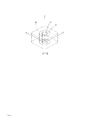
(第1實施形態) 圖1係模式性地表示本發明之第1實施形態之共振器之剖視圖,圖2係自圖1之切斷面線II-II觀察之剖視圖。再者,於以下之說明中,設想相互正交之X軸、Y軸、Z軸之3軸座標系統進行敍述。 (First Embodiment) Fig. 1 is a cross-sectional view schematically showing the resonator according to the first embodiment of the present invention, and Fig. 2 is a cross-sectional view taken from the section line II-II of Fig. 1. Furthermore, in the following description, a three-axis coordinate system of X-axis, Y-axis, and Z-axis orthogonal to each other is assumed to be described.
本實施形態之共振器包含屏蔽殼體10、第1共振元件11、及第2共振元件12。屏蔽殼體10具有第1導體部13及第2導體部14。第1共振元件11可使用金屬及非金屬導電性物質等既知之各種導電性材料形成。為了提高共振器之特性,例如,可使用以Ag、Ag-Pd、Ag-Pt等Ag合金為主成分之導電性材料,或者Cu系、W系、Mo系、Pd系之導電性材料等。The resonator of this embodiment includes a
屏蔽殼體10具有於內部具有空腔19之長方體狀之箱體之形狀,且連接於基準電位。基準電位係指被稱為接地(ground)電位、接地(earth)電位或接地電位之電位。屏蔽殼體10係將位於作為第1方向之-Z方向(於圖1中為下方)側之第1導體部13與位於作為第2方向之+Z方向(於圖1中為上方)側之第2導體部14藉由導電性接合材接合而構成。第1導體部13係由4個側壁部與底部構成,且呈+Z方向側開口之長方體之箱狀之形狀。第2導體部14呈矩形之平板狀之形狀。又,於第1導體部13之對向之2個側壁部,形成用於與外部電路之連接之貫通孔16及貫通孔17。The
第1導體部13及第2導體部14可使用如金屬及非金屬導電性物質般之既知之各種導電性材料形成。為了提高共振器之特性,例如,可使用以Ag、Ag-Pd、Ag-Pt等Ag合金為主成分之導電性材料,或Cu系、W系、Mo系或Pd系之導電性材料等。The
作為將第1導體部13與第2導體部14接合之導電性接合材,可使用焊料或導電性接著劑等各種既知之導電性接合材。根據情況,亦可藉由螺絲或螺栓而將第1導體部13與第2導體部14緊固後接合。又,空腔19內充滿空氣,但亦可為真空,亦可充滿空氣以外之氣體,例如惰性氣體。As the conductive bonding material for bonding the
於圖2所示之俯視時,第1共振元件11配置於空腔19之中央,且具有於±Z方向延伸之圓柱狀之形狀。又,第1共振元件11係將作為第1方向之-Z方向之端藉由導電性接合材而接合於第1導體部13。而且,於第1共振元件11之作為第2方向之+Z方向之端與屏蔽殼體10之第2導電部14之間,存在間隔δ1。即,第1共振元件11之-Z方向之表面之整體接合於第1導體部13之底部,且第1共振元件11之+Z方向之表面與屏蔽殼體10之第2導體部14之間藉由間隔δ1而隔開。In the plan view shown in FIG. 2, the
於本實施形態中,第1共振元件11包含導體,本實施形態之共振器作為具有類似於TEM模式之共振模式之共振器發揮功能。In this embodiment, the
本實施形態之第1共振元件11可使用如金屬或非金屬導電性物質般之既知之各種導電性材料形成。為了提高共振器之特性,例如,可適當選擇使用以Ag、Ag-Pd、Ag-Pt等Ag合金為主成分之導電性材料,或Cu系、W系、Mo系、Pd系之導電性材料等。再者,第1共振元件11亦可為於柱狀之介電體或絕緣體之表面具有導電體層者。作為第1共振元件11之材質,亦可於環氧樹脂等樹脂被覆導體層而使用。The
於空腔19之中央,第2共振元件12配置於與第1共振元件11為同一軸線上,且具有於±Z方向延伸之圓筒狀之形狀。而且,第1共振元件11位於第2共振元件12之內側之中央。即,第2共振元件12與第1共振元件11於一半徑線方向空開間隔δ2包圍第1共振元件11。又,第2共振元件12係將作為第2方向之+Z方向之端藉由導電性接合材而接合於第2導體部14。而且,於第2共振元件12之-Z方向之端與屏蔽殼體10之間存在間隔δ3。即,第2共振元件12之+Z方向之表面之整體接合於第2導體部14,第2共振元件12之-Z方向之表面與屏蔽殼體10之第1導體部13之間藉由間隔δ3而隔開。In the center of the
第1共振元件11之+Z方向之長度可為空腔19之+Z方向之尺寸之80%以上,亦可為空腔19之+Z方向之尺寸之90%以上。又,第1共振元件11之±Z方向上之一半以上之部分可由第2共振元件12包圍。第1共振元件11中之由第2共振元件12包圍之部分之+Z方向之長度相對於第1共振元件11之+Z方向之長度的比率可為50%以上。進而,自提高電氣特性之觀點而言,上述比率亦可為80%以上,若設為90%以上,則電氣特性進而提高。其理由在於,作為本共振模式之原理,利用第1共振元件11與第2共振元件12之奇偶模之耦合。於該情形時,+Z方向之長度之比率越長則奇偶模之耦合越強,奇偶模之共振頻率分離。此時,可根據第2共振元件12之介電體之體積,進一步降低頻率。進而,藉由調整第2共振元件12之介電體,而使向第1共振元件11之磁場集中緩和,藉由向第2共振元件12擴大磁場可提高Q值。因此, +Z方向之長度之比率某種程度上較長有所重要。空腔19之大小、第1共振元件11之直徑、第1共振元件11與第2共振元件12之間隔δ2及第2共振元件12之厚度係根據所期望之尺寸、基本模式共振之共振頻率及高次模式共振之共振頻率而適當設定。The length of the
作為第2共振元件12之材質,可使用介電陶瓷等既知之介電材料。例如,可適當地使用含有BaTiO
3、Pb
4Fe
2Nb
2O
12、TiO
2等之介電陶瓷材料。根據情況,亦可使用環氧樹脂等樹脂。作為將第2共振元件12與屏蔽殼體10接合之導電性接合材,例如可使用如導電性接著劑般之各種既知之導電性接合材。
As the material of the
此種第2共振元件12具有:內壁被覆層3,其形成於內壁面且包含導體;端壁被覆層4,其形成於作為第1方向之-Z方向之端且包含導體;及接合端被覆層5,其形成於作為第2方向之+Z方向之端且包含導體。該等內壁被覆層3、端壁被覆層4及接合端被覆層5可適當選擇使用與第1共振元件11相同之材料,即以Ag、Ag-Pd、Ag-Pt等Ag合金為主成分之導電性材料,或Cu系、W系、Mo系、Pd系之導電性材料等,且藉由金屬化處理,而形成為例如厚度5~20 μm之導電膜。作為最低限度之膜厚,必須較所使用之頻率之表皮效果之厚度厚。接合端被覆層5與屏蔽殼體10亦可使用焊料等接合。於該情形時,接合端被覆層5及焊料作為導電性接合材發揮功能。Such a
此種本實施形態之共振器具有屏蔽殼體10、第1共振元件11、及第2共振元件12。屏蔽殼體10包含位於-Z方向側之第1導體部13及位於作為與-Z方向相反方向之+Z方向側之第2導體部14而構成,且於內部具有空腔19。第1共振元件11包含導體,具有柱狀之形狀,處於空腔19內,-Z方向之端接合於第1導體部13,於+Z方向之端與屏蔽殼體10之間具有間隔。第2共振元件12處於空腔19內,+Z方向之端接合於第2導體部14,於-Z方向之端與屏蔽殼體10之間具有間隔,且與第1共振元件11空開間隔地包圍第1共振元件11。具有此種構成之本實施形態之共振器作為具有與TEM模式類似之共振模式之共振器發揮功能。The resonator of this embodiment includes a
上述專利文獻1等中所記載之先前技術之共振器存在難以小型化之問題。而且,若藉由將介電體填充至屏蔽盒之內側之整體而小型化,則高次模式共振之共振頻率會大幅度降低並接近基本模式共振之共振頻率,從而存在電氣特性惡化之問題。又,若於作為第1共振元件之柱狀導體之開放端與屏蔽盒之間配置介電體而小型化,則Q值會大幅度降低,從而存在電氣特性惡化之問題。The prior art resonator described in
相對於此種先前技術之共振器,上述本實施形態之共振器可較專利文獻1等先前技術之共振器更小型化,可較於專利文獻1等先前技術之共振器之屏蔽盒之內側整體填充介電體者更抑制高次模式共振之共振頻率之降低,進而可較於專利文獻1等先前技術之共振器之柱狀導體之開放端與屏蔽盒之間配置介電體者更抑制Q值之降低。即,本實施形態之共振器係基本模式共振之共振頻率與高次模式共振之共振頻率之差較大,Q值較高,且具有優異之電氣特性並且小型。即,本實施形態之共振器小型且電氣特性優異。Compared with the resonator of the prior art, the resonator of the above-mentioned present embodiment can be smaller in size than the resonator of the prior art such as
又,具有上述構成之本實施形態之共振器例如可以如下之方式製作。首先,製作將第1共振元件11之-Z方向之端接合於第1導體部13之構造體。又,製作將第2共振元件12之+Z方向之端接合於第2導體部14之構造體。然後,以第1共振元件11位於第2共振元件12之內側之方式,將上述第1導體部13與第2導體部14接合,藉此可製造本實施形態之共振器。因此,可容易地製造第1共振元件11之-Z方向之端確實地接合於第1導體部13、第2共振元件12之+Z方向之端確實地接合於第2導體部14且可靠性較高之共振器。In addition, the resonator of the present embodiment having the above-mentioned structure can be manufactured as follows, for example. First, a structure in which the end of the
又,於本實施形態之共振器中,第2共振元件12具有筒狀之形狀。因此,藉由具有單純之形狀之1個第2共振元件12,可空開間隔地包圍第1共振元件11之周圍,故而進而量產性優異。In addition, in the resonator of this embodiment, the
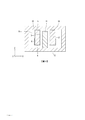
圖3係表示模擬第1實施形態之共振器之數值解析模型之立體圖,圖4A係表示模擬第1實施形態之共振器之數值解析模型之解析結果即電場分佈的圖,圖4B係表示第1實施形態之共振器之數值解析模型之解析結果即磁場分佈的圖。再者,本案發明者於藉由使用電腦之數值解析而模擬如圖1及圖2所示之第1實施形態之共振器之電性特性及磁性特性時,將共振器之貫通孔16、17省略後進行解析處理。Fig. 3 is a perspective view showing the numerical analysis model of the resonator in the first embodiment. Fig. 4A shows the electric field distribution, which is the analysis result of the resonator in the first embodiment. Fig. 4B shows the first embodiment. The analysis result of the numerical analysis model of the resonator of the embodiment is a graph of the magnetic field distribution. Furthermore, the inventor of the present invention simulated the electrical and magnetic characteristics of the resonator of the first embodiment shown in FIG. 1 and FIG. 2 by numerical analysis using a computer, and the through
於數值解析模型中,構成第2共振元件12之介電體係將相對介電常數設為43,介電損耗正切設為3×10
-5。第1導體部13、第2導體部14及第1共振元件11之導電率設為4.2×10
7S/m。空腔19之+X方向之尺寸及+Y方向之尺寸設為38 mm,空腔19之+Z方向之尺寸設為20 mm。第1共振元件11之直徑設為9 mm,第1共振元件11之長度(+Z方向之尺寸)設為19 mm。第2共振元件12之內徑設為11 mm,第2共振元件12之外徑設為20 mm,第2共振元件12之長度(+Z方向之尺寸)設為19 mm。於該數值解析模型中,設為具備內壁被覆層3及端壁被覆層4但不具備外壁被覆層6之構成。內壁被覆層3及端壁被覆層4之厚度設為10 μm。
In the numerical analysis model, the relative dielectric constant of the dielectric system constituting the
模擬之結果,基本模式共振之共振頻率為670 MHz,基本模式共振之Q值為2952。頻率最低之高次模式共振之共振頻率為2.74 GHz,高次模式共振之共振頻率為2.95 GHz。此處,該高次模式為運用介電體之模式,並非運用本原理之奇偶模中之一個。於本發明之構造中,由於介電體之體積較少,故而根據解析可知較一般的介電體共振器而言高次模式較高。As a result of the simulation, the resonance frequency of the fundamental mode resonance is 670 MHz, and the Q value of the fundamental mode resonance is 2952. The resonance frequency of the lowest frequency high-order mode resonance is 2.74 GHz, and the resonance frequency of the high-order mode resonance is 2.95 GHz. Here, the higher-order mode is a mode using a dielectric, and it is not one of the odd-even modes using this principle. In the structure of the present invention, since the volume of the dielectric body is small, the analysis shows that the higher order mode is higher than that of the general dielectric body resonator.
圖5A係表示藉由模擬自第2共振元件12去除內壁被覆層3及端壁被覆層4之無被覆導體之共振器的比較例1之共振器之數值解析模型而對電場、磁場特性進行數值解析時之電場分佈的圖,圖5B係表示藉由比較例1之共振器之數值解析模型而對電場、磁場特性進行數值解析時之磁場分佈的圖。於比較例1之共振器之數值解析模型中,共振器之各尺寸及各物性與第1實施形態之共振器相同,藉由設想自第2共振元件12去除內壁被覆層3及端壁被覆層4之構成之數值解析模型而進行數值解析。FIG. 5A shows the numerical analysis model of the resonator of Comparative Example 1 in which the inner
於比較例1中進行數值解析之結果為,基本模式共振之共振頻率為1.05 GHz,基本模式共振之Q值為3828。高次模式共振之共振頻率為2.63 GHz,最低之頻率之高次模式共振之Q值為2612。The result of numerical analysis in Comparative Example 1 shows that the resonance frequency of the fundamental mode resonance is 1.05 GHz, and the Q value of the fundamental mode resonance is 3828. The resonance frequency of the high-order mode resonance is 2.63 GHz, and the Q value of the low-order mode resonance is 2612.
根據該等結果,確認到比較例1之共振器中,磁場分佈與先前之1/4波長半同軸共振器同等,但關於電場分佈,基本模式共振及高次模式共振之任一者之共振頻率均降低,但較第1實施形態之共振器之共振頻率高。當然,為了降低頻率,必須使共振器之尺寸變大。Based on these results, it was confirmed that in the resonator of Comparative Example 1, the magnetic field distribution is the same as that of the previous quarter-wavelength semi-coaxial resonator, but the electric field distribution, the resonance frequency of any one of the fundamental mode resonance and the high-order mode resonance Both are lower, but higher than the resonance frequency of the resonator of the first embodiment. Of course, in order to reduce the frequency, the size of the resonator must be increased.
圖6A係表示藉由模擬使第2共振元件12之介電體為空氣、於內表面具有內壁被覆層3之共振器的比較例2之共振器之數值解析模型而對電場、磁場特性進行數值解析時之電場分佈的圖,圖6B係表示藉由比較例2之共振器之數值解析模型而對電場、磁場特性進行數值解析時之磁場分佈的圖。於比較例2之共振器之數值解析模型中,藉由設想使共振器之各尺寸與第1實施形態之共振器相同且自第2共振元件12去除端壁被覆層4之構成之數值解析模型而進行數值解析。6A shows the numerical analysis model of the resonator of Comparative Example 2 in which the dielectric of the second
比較例2之數值解析之結果為,基本模式共振之共振頻率為0.81 GHz,基本模式共振之Q值為3206。頻率最低之高次模式共振之共振頻率為7.88 GHz,高次模式共振之Q值為4244。The result of the numerical analysis of Comparative Example 2 is that the resonance frequency of the fundamental mode resonance is 0.81 GHz, and the Q value of the fundamental mode resonance is 3206. The resonance frequency of the lowest high-order mode resonance is 7.88 GHz, and the Q value of the high-order mode resonance is 4244.
根據該等結果,確認到比較例2之共振器中,金屬間磁場分佈較高,但基本上保持第1實施形態之共振器之磁場分佈之特徵,基本模式共振及高次模式共振之任一者之共振頻率均變高。Based on these results, it is confirmed that the resonator of Comparative Example 2 has a high magnetic field distribution between metals, but basically maintains the characteristics of the magnetic field distribution of the resonator of the first embodiment, either the fundamental mode resonance or the higher mode resonance The resonance frequency of both becomes higher.
圖7A係表示藉由模擬使第2共振元件12之介電體為金屬、去除內壁被覆層3及端壁被覆層4之共振器的比較例3之共振器之數值解析模型而對電場、磁場特性進行數值解析時之電場分佈的圖,圖7B係表示藉由比較例3之共振器之數值解析模型而對電場、磁場特性進行數值解析時之磁場分佈的圖。於比較例3之共振器之數值解析模型中,設想使第2共振元件12之介電體為金屬且去除端壁被覆層4,除此以外與第1實施形態之共振器之數值解析模型相同之構成,進行算出電場、磁場特性之數值解析。FIG. 7A shows the numerical analysis model of the resonator of Comparative Example 3 in which the dielectric of the
比較例3之數值解析之結果為,基本模式共振之共振頻率為0.95 GHz,基本模式共振之Q值為1902。頻率最低之高次模式共振之共振頻率為6.74 GHz,高次模式共振之Q值為1459。The result of the numerical analysis of Comparative Example 3 is that the resonance frequency of the fundamental mode resonance is 0.95 GHz, and the Q value of the fundamental mode resonance is 1902. The resonance frequency of the lowest high-order mode resonance is 6.74 GHz, and the Q value of the high-order mode resonance is 1459.
根據該等結果,確認到比較例3之共振器中,導體間之磁場變高,導體之周圍之磁場消失,故而Q值降低,基本模式共振及高次模式共振之任一者之共振頻率均變高。According to these results, it was confirmed that in the resonator of Comparative Example 3, the magnetic field between the conductors became higher and the magnetic field around the conductors disappeared, so the Q value was lowered. The resonance frequencies of either the fundamental mode resonance and the higher-order mode resonance were both Becomes high.
(第2實施形態)
圖8係模式性地表示本發明之第2實施形態之共振器之剖視圖。再者,對與上述實施形態對應之部分標註相同之參照符號。本實施形態之共振器係於上述第1實施形態之共振器之第2共振元件12中具有內壁被覆層3但不具有端壁被覆層4之方面不同,其他之構成相同。
(Second Embodiment)
Fig. 8 is a cross-sectional view schematically showing the resonator according to the second embodiment of the present invention. In addition, the same reference numerals are given to the parts corresponding to the above-mentioned embodiment. The resonator of this embodiment is different from the second
圖9A係表示使用模擬第2實施形態之共振器之數值解析模型之解析結果即電場分佈的圖,圖9B係表示使用第2實施形態之共振器之數值解析模型之解析結果即磁場分佈的圖。第2實施形態之共振器之數值解析之結果為,基本模式共振之共振頻率為0.72 GHz,基本模式共振之Q值為2987。頻率最低之高次模式共振之共振頻率為2.92 GHz,高次模式共振之Q值為2071。Fig. 9A is a diagram showing the electric field distribution which is the analysis result of the numerical analysis model using the resonator of the second embodiment, and Fig. 9B is a diagram showing the magnetic field distribution which is the analysis result of the numerical analysis model using the resonator of the second embodiment . As a result of the numerical analysis of the resonator of the second embodiment, the resonance frequency of the fundamental mode resonance is 0.72 GHz, and the Q value of the fundamental mode resonance is 2987. The resonance frequency of the lowest frequency high-order mode resonance is 2.92 GHz, and the Q value of the high-order mode resonance is 2071.
根據該等結果,確認到於電場分佈中,第2共振元件12之作為第1方向之-Z方向之端之電場強度變高而低頻化,於磁場分佈中,-Z方向之端之磁場強度較低,尤其於第1共振元件11與內壁被覆層3之間之導體間之磁場強度變低而高Q值化,Q值變高。Based on these results, it was confirmed that in the electric field distribution, the electric field intensity at the end of the -Z direction as the first direction of the second
(第3實施形態)
圖10係模式性地表示本發明之第3實施形態之共振器之剖視圖。再者,對與上述實施形態對應之部分標註相同之參照符號。本實施形態之共振器係於上述第1實施形態之共振器之第2共振元件12中,除了內壁被覆層3、端壁被覆層4、接合端被覆層5以外,還具有自-Z方向之端朝向+Z方向覆蓋全長之約一半之位置的外壁被覆層6,其他之構成相同。
(Third Embodiment)
Fig. 10 is a cross-sectional view schematically showing a resonator according to a third embodiment of the present invention. In addition, the same reference numerals are given to the parts corresponding to the above-mentioned embodiment. The resonator of this embodiment is based on the second
(第4實施形態)
圖11係模式性地表示本發明之第4實施形態之共振器之剖視圖。再者,對與上述實施形態對應之部分標註相同之參照符號。本實施形態之共振器係具有與上述第3實施形態之共振器類似之構成,但於外壁被覆層6設置於向+Z方向側偏移之位置之方面不同。
(Fourth Embodiment)
Fig. 11 is a cross-sectional view schematically showing a resonator according to a fourth embodiment of the present invention. In addition, the same reference numerals are given to the parts corresponding to the above-mentioned embodiment. The resonator of this embodiment has a similar structure to the resonator of the third embodiment described above, but is different in that the outer
圖12係表示使用模擬第4實施形態之共振器之數值解析模型之解析結果之磁場分佈的圖。再者,對與上述實施形態對應之部分標註相同之參照符號。第4實施形態之共振器之數值解析之結果為,基本模式共振之共振頻率為0.68 GHz,基本模式共振之Q值為2824。頻率最低之高次模式共振之共振頻率為1.01 GHz,高次模式共振之Q值為278。Fig. 12 is a diagram showing a magnetic field distribution using a numerical analysis model that simulates the resonator of the fourth embodiment. In addition, the same reference numerals are given to the parts corresponding to the above-mentioned embodiment. As a result of the numerical analysis of the resonator of the fourth embodiment, the resonance frequency of the fundamental mode resonance is 0.68 GHz, and the Q value of the fundamental mode resonance is 2824. The resonance frequency of the lowest frequency high-order mode resonance is 1.01 GHz, and the Q value of the high-order mode resonance is 278.
根據該等結果,確認到第4實施形態之共振器與第3實施形態之共振器相比,更低頻化,無較大之Q值之降低。Based on these results, it was confirmed that the resonator of the fourth embodiment has a lower frequency than the resonator of the third embodiment, and there is no significant decrease in the Q value.
(第5實施形態)
圖13係模式性地表示本發明之第5實施形態之共振器之剖視圖。再者,對與上述實施形態對應之部分標註相同之參照符號。本實施形態之共振器係具有與上述第4實施形態之共振器類似之構成,但除了內壁被覆層3、端壁被覆層4、接合端被覆層5以外,還具有自+Z方向之端朝向-Z方向覆蓋全長之約一半之位置的外壁被覆層6,其他之構成相同。
(Fifth Embodiment)
Fig. 13 is a cross-sectional view schematically showing a resonator according to a fifth embodiment of the present invention. In addition, the same reference numerals are given to the parts corresponding to the above-mentioned embodiment. The resonator of this embodiment has a similar structure to the resonator of the fourth embodiment, but in addition to the inner
圖14係表示使用模擬第5實施形態之共振器之數值解析模型之解析結果之磁場分佈額圖。第5實施形態之共振器之數值解析之結果為,基本模式共振之共振頻率為0.64 GHz,基本模式共振之Q值為2115。頻率最低之高次模式共振之共振頻率為1.47 GHz,高次模式共振之Q值為1128。Fig. 14 is a diagram showing the distribution of the magnetic field using the numerical analysis model that simulates the resonator of the fifth embodiment. As a result of the numerical analysis of the resonator of the fifth embodiment, the resonance frequency of the fundamental mode resonance is 0.64 GHz, and the Q value of the fundamental mode resonance is 2115. The resonance frequency of the lowest frequency high-order mode resonance is 1.47 GHz, and the Q value of the high-order mode resonance is 1128.
根據該等結果,確認到第5實施形態之共振器與第4實施形態之共振器相比,更低頻化,低Q值化,但無較大之Q值之降低。Based on these results, it was confirmed that the resonator of the fifth embodiment has a lower frequency and a lower Q than the resonator of the fourth embodiment, but there is no significant decrease in the Q value.
(第6實施形態)
圖15係模式性地表示本發明之第6實施形態之共振器之剖視圖。再者,對與上述實施形態對應之部分標註相同之參照符號。本實施形態之共振器具備:屏蔽殼體10,其包含位於作為第1方向之-Z方向側之第1導體部13、及位於作為與-Z方向相反方向之+Z方向側之第2導體部14,且於內部具有空腔19;第1共振元件11,其包含介電體或導體,具有柱狀之形狀,位於空腔19內,-Z方向之端接合於第1導體部13,於+Z方向之端與屏蔽殼體10之間具有間隔δ1;及第2共振元件12,其位於空腔19內,+Z方向之端接合於第2導體部14,於-Z方向之端與屏蔽殼體10之間具有間隔δ3,與第1共振元件11空開間隔δ2包圍第1共振元件11。
(The sixth embodiment)
Fig. 15 is a cross-sectional view schematically showing a resonator according to a sixth embodiment of the present invention. In addition, the same reference numerals are given to the parts corresponding to the above-mentioned embodiment. The resonator of this embodiment includes a
第2共振元件12於內壁面具有包含導體之內壁被覆層3,於-Z方向之端具有包含導體之端壁被覆層4,於+Z方向之端具有包含導體之接合端被覆層5。於空開間隔δ3隔開之第1導體部13與第2共振元件12之-Z方向之端之間,設置包括低介電常數之介電體之支持部7。支持部7亦可為短圓筒狀,亦可將複數個單片以等角度空開間隔地配設。The
藉由設置此種支持部7,能夠使第2共振元件12壓接而取得導通。此時,支持部7之材料亦可為聚四氟乙烯等低損耗且能夠稍微變形者。By providing such a
(第7實施形態)
圖16係模式性地表示本發明之第7實施形態之共振器之剖視圖。再者,本實施形態之共振器與上述第6實施形態類似,對所對應之部分標註相同之參照符號。具備屏蔽殼體10、第1共振元件11及第2共振元件12,進而於第2導體部14與第1共振元件11之+Z方向之端之間,設置包含介電體之按壓部8。按壓部8例如亦可藉由短圓柱狀之單片而實現。
(The seventh embodiment)
Fig. 16 is a cross-sectional view schematically showing the resonator according to the seventh embodiment of the present invention. In addition, the resonator of this embodiment is similar to the sixth embodiment described above, and the corresponding parts are denoted by the same reference numerals. The
藉由設置此種按壓部8,能夠進一步降低共振頻率。按壓部8之材料亦可為陶瓷或聚四氟乙烯等低損耗者。By providing such a
(第8實施形態)
圖17係模式性地表示本發明之第8實施形態之共振器之剖視圖。再者,本實施形態之共振器與上述第6實施形態之共振器類似,對所對應之部分標註相同之參照符號。本實施形態之共振器具備屏蔽殼體10、第1共振元件11及第2共振元件12,進而於第2共振元件12之+Z方向之端之接合端被覆層5與第2導體部14之間,設置有成為形成接合端被覆層5之一部分之供焊料流入之焊料積存部之環狀之凹槽部23。又,相反,亦可於屏蔽殼體10側具有凹槽部。
(Eighth Embodiment)
Fig. 17 is a cross-sectional view schematically showing the resonator according to the eighth embodiment of the present invention. In addition, the resonator of this embodiment is similar to the resonator of the above-mentioned sixth embodiment, and the corresponding parts are denoted by the same reference numerals. The resonator of this embodiment includes a
藉由設置此種凹槽部23,可防止焊料向導體被膜之外側露出而導致改變導體之面積。一般而言,相同之效果亦可藉由於導體被膜之上在連接部以外之場所設置外覆玻璃而獲得。By providing such a recessed
(第9實施形態)
圖18係模式性地表示本發明之第9實施形態之共振器之剖視圖。再者,本實施形態之共振器與上述第6實施形態類似,對所對應之部分標註相同之參照符號。本實施形態之共振器具備屏蔽殼體10、第1共振元件11及第2共振元件12,進而設置頻率調整件9,該頻率調整件9設置於第2導體部14,包含導體,用以使相對於第1共振元件11之-Z方向或+Z方向之重疊量變化而調整頻率。第1共振元件11形成為於+Z方向開放之有底筒狀,於中央之孔移動自如地可動嵌合有頻率調整件9。第1共振元件11之底部藉由螺絲構件24而固定於第1導體部13。
(Ninth Embodiment)
Fig. 18 is a cross-sectional view schematically showing a resonator according to a ninth embodiment of the present invention. In addition, the resonator of this embodiment is similar to the sixth embodiment described above, and the corresponding parts are denoted by the same reference numerals. The resonator of this embodiment includes a shielding
此種頻率調整件9例如藉由金屬製之螺栓而實現。藉由使頻率調整件9相對於第2導體部14螺進/螺退,可調整共振頻率。Such a
(第10實施形態)
圖19係模式性地表示本發明之第10實施形態之共振器之剖視圖。再者,對與上述實施形態對應之部分標註相同之參照符號。本實施形態之共振器具備:屏蔽殼體10,其包含位於作為第1方向之-Z方向側之第1導體部13、及位於作為與-Z方向相反方向之+Z方向側之第2導體部14,且於內部具有空腔19;第1共振元件11a,其包含介電體或導體,具有柱狀之形狀,位於空腔19內,-Z方向之端接合於第1導體部13;及第2共振元件12,位於空腔19內,+Z方向之端接合於第1導體部14,於-Z方向之端與屏蔽殼體10之第1導體部13之間具有間隔δ3,與第1共振元件11空開間隔δ2包圍第1共振元件11。
(Tenth Embodiment)
Fig. 19 is a cross-sectional view schematically showing the resonator according to the tenth embodiment of the present invention. In addition, the same reference numerals are given to the parts corresponding to the above-mentioned embodiment. The resonator of this embodiment includes a
進而,本實施形態之共振器設置有頻率調整件9a,該頻率調整件9a設置於第2導體部14且包含導體。第1共振元件11a形成為於+Z方向開放之有底筒狀,於中央之孔移動自如地可動嵌合有頻率調整件9a。第1共振元件11a可使第1導體部13貫通於與-Z方向及+Z方向平行之厚度方向而螺合,使與頻率調整件9a之重疊量變化,調整共振頻率。Furthermore, the resonator of this embodiment is provided with the
圖20A~圖20C係用以說明利用頻率調整件實現之頻率之變化量之圖,圖20A係未設置頻率調整件9之共振器模式化後之剖視圖,圖20B係表示使頻率調整件9自第2導體部14向空腔19內突出僅2 mm之狀態,圖20C係表示使頻率調整件9自第2導體部14向空腔19內突出僅4 mm之狀態。Figures 20A to 20C are diagrams for explaining the amount of change in frequency achieved by the frequency adjustment element. Figure 20A is a cross-sectional view of the resonator without the
如此使頻率調整件9向空腔19內之突出量變化時,於突出量為2 mm之情形時,共振頻率之變化量為0.007 GHz,於突出量為4 mm之情形時,共振頻率之變化量為0.014 GHz。藉此,確認到可根據頻率調整件9之空腔19內之露出量來調整共振頻率。In this way, when the protrusion amount of the
(第11實施形態)
圖21係模式性地表示本發明之第11實施形態之共振器之剖視圖。再者,對與上述實施形態對應之部分標註相同之參照符號。本實施形態之共振器於第2共振元件12之+Z方向之端與第2導體部14之間,設置包括作為導體之金屬之台座部25。
(Eleventh embodiment)
Fig. 21 is a cross-sectional view schematically showing the resonator according to the eleventh embodiment of the present invention. In addition, the same reference numerals are given to the parts corresponding to the above-mentioned embodiment. The resonator of this embodiment is provided with a
藉由此種構成,能夠事前將介電體與台座部25連接。藉由使用相對於殼體之大小充分小之台座部25,可容易地進行焊料連接時之加熱。With this structure, the dielectric body can be connected to the base 25 in advance. By using the
(濾波器)
圖22係模式性地表示本發明之濾波器之一實施形態之立體圖,圖23係圖22所示之濾波器之剖視圖。本實施形態之濾波器包含複數個作為共振器之第1及第2共振器20a、20b、第1端子部18a、及第2端子部18b而構成。第1共振器20a及第2共振器20b具有與上述圖1~圖21所示之共振器相同之構造。又,第1共振器20a及第2共振器20b以電磁性地耦合之方式成行配置。第1共振器20a位於行之一端,第2共振器20b位於行之另一端。第1端子部28a電磁性地連接於第1共振器20a,第2端子部28b電磁性地連接於第2共振器20b。由於具有此種構成,故而本實施形態之濾波器能夠實現小型化,並且可實現通帶之插入損耗較小且通帶附近之衰減量較大之優異特性。
(filter)
FIG. 22 is a perspective view schematically showing an embodiment of the filter of the present invention, and FIG. 23 is a cross-sectional view of the filter shown in FIG. 22. The filter of the present embodiment includes a plurality of first and
圖24係表示使用上述第2實施形態之共振器作為第1及第2共振器20a、20b之情形時之濾波器之頻率特性的曲線圖。根據曲線圖可知,獲得透過特性S21於725 MHz時通過、且反射特性S11亦為-20 dB以下之良好之濾波器特性,表示使用本發明之共振器可構成濾波器。FIG. 24 is a graph showing the frequency characteristics of the filter when the resonator of the second embodiment described above is used as the first and
(通信裝置)
圖25係模式性地表示本發明之通信裝置之一實施形態之方塊圖。本實施形態之通信裝置具有天線82、通信電路81、以及連接於天線82及通信電路81之濾波器80。濾波器80為上述一實施形態之濾波器。天線82及通信電路81為既知之先前之天線及通信電路。
(Communication device)
Fig. 25 is a block diagram schematically showing an embodiment of the communication device of the present invention. The communication device of this embodiment has an
具有此種構成之本實施形態之通信裝置由於使用小型且電氣特性優異之上述濾波器將不需要之電氣信號去除,故而能夠實現小型化,且可使通信品質良好。The communication device of the present embodiment having such a configuration uses the above-mentioned filter having a small size and excellent electrical characteristics to remove unnecessary electrical signals, so that the size can be reduced and the communication quality can be improved.
本發明並不限定於上述實施形態,按照本發明之技術思想能夠進行各種變更及改良。The present invention is not limited to the above-mentioned embodiment, and various changes and improvements can be made according to the technical idea of the present invention.
例如,於上述實施形態中,表示了第1共振元件11具有圓柱狀之形狀之示例,但並不限定於此。第1共振元件11例如亦可具有4角柱狀、6角柱狀、橢圓柱狀等其他形狀。又,亦可如專利文獻1中所記載之共振器般,第1共振元件11係剖面面積並不固定之形狀。For example, in the above-mentioned embodiment, the example in which the
又,於上述實施形態中,表示了1個筒狀之第2共振元件12包圍第1共振元件11之示例,但並不限定於此。例如,亦可為狹縫於+Z方向貫通第2共振元件12,而將第2共振元件12為分割4個部分。即,亦可為具有複數個第2共振元件12,且複數個第2共振元件12以包圍柱狀體21之方式配置。In addition, in the above-mentioned embodiment, the example in which one cylindrical second
又,於上述一實施形態之濾波器中,表示了第1共振器20a及第2共振器20b具有與第2實施形態之共振器相同之構造之情形,但並不限定於此。例如,亦可具有與第1實施形態或第3實施形態~第13實施形態之任一個共振器相同之構造,亦可具有其他構造。In addition, in the filter of the aforementioned embodiment, the
又,於上述實施形態中,表示了濾波器具有2個共振器20a、20b之示例,但並不限定於此。濾波器亦可具有3個以上之共振器。於該情形時,亦可於第1共振器20a與第2共振器20b之間,配置其他共振器,以所有共振器電磁耦合之方式構成。又,亦可藉由如通常之濾波器設計般形成共振器間以外之跳躍耦合,而構成衰減極。
本發明可於不脫離其精神或主要特徵之情況下,以其他各種形態實施。因此,上述實施形態於所有方面只不過為單純之例示,本發明之範圍係申請專利範圍所示者,並不受說明書本文之任何拘束。進而,屬於申請專利範圍之變化或變更全部為本發明之範圍內者。
Furthermore, in the above-mentioned embodiment, an example in which the filter has two
3 內壁被覆層
4 端壁被覆層
5 接合端被覆層
6 外壁被覆層
7 支持部
8 按壓部
9 頻率調整件
9a 頻率調整件
10 屏蔽殼體
11 第1共振元件
11a 第1共振元件
12 第2共振元件
13 第1導體部
14 第2導體部
16 貫通孔
17 貫通孔
18a 第1端子部
18b 第2端子部
19 空腔
20a 第1共振器
20b 第2共振器
23 凹槽部
24 螺絲構件
25 台座部
80 濾波器
81 通信電路
82 天線
δ1 間隔
δ2 間隔
δ3 間隔
3 Inner
本發明之目的、特色、及優點根據下述詳細之說明與圖式而更明確。
圖1係模式性地表示本發明之第1實施形態之共振器之剖視圖。
圖2係自圖1之切斷面線II-II觀察之剖視圖。
圖3係表示模擬第1實施形態之共振器之數值解析模型之立體圖。
圖4A係表示模擬第1實施形態之共振器之數值解析模型之解析結果即電場分佈之圖。
圖4B係表示第1實施形態之共振器之數值解析模型之解析結果即磁場分佈之圖。
圖5A係表示藉由模擬自第2共振元件12去除內壁被覆層3及端壁被覆層4之無被覆導體之共振器的比較例1之共振器之數值解析模型而對電場、磁場特性進行數值解析時之電場分佈的圖。
圖5B係表示藉由比較例1之共振器之數值解析模型而對電場、磁場特性進行數值解析時之磁場分佈的圖。
圖6A係表示藉由模擬使第2共振元件12之介電體為空氣、於內表面具有內壁被覆層3之共振器的比較例2之共振器之數值解析模型而對電場、磁場特性進行數值解析時之電場分佈的圖。
圖6B係表示藉由比較例2之共振器之數值解析模型而對電場、磁場特性進行數值解析時之磁場分佈的圖。
圖7A係表示藉由模擬使第2共振元件12之介電體為金屬、去除內壁被覆層3及端壁被覆層4之共振器的比較例3之共振器之數值解析模型而對電場、磁場特性進行數值解析時之電場分佈的圖。
圖7B係表示藉由比較例3之共振器之數值解析模型而對電場、磁場特性進行數值解析時之磁場分佈的圖。
The purpose, features, and advantages of the present invention are more clarified based on the following detailed description and drawings.
Fig. 1 is a cross-sectional view schematically showing the resonator according to the first embodiment of the present invention.
Fig. 2 is a cross-sectional view taken from the section line II-II of Fig. 1.
Fig. 3 is a perspective view showing a numerical analysis model that simulates the resonator of the first embodiment.
FIG. 4A is a diagram showing the analysis result of the numerical analysis model of the resonator of the first embodiment, that is, the electric field distribution.
4B is a diagram showing the analysis result of the numerical analysis model of the resonator of the first embodiment, that is, the magnetic field distribution.
FIG. 5A shows the numerical analysis model of the resonator of Comparative Example 1 in which the inner
圖8係模式性地表示本發明之第2實施形態之共振器之剖視圖。
圖9A係表示使用模擬第2實施形態之共振器之數值解析模型之解析結果即電場分佈的圖。
圖9B係表示使用第2實施形態之共振器之數值解析模型之解析結果即磁場分佈的圖。
圖10係模式性地表示本發明之第3實施形態之共振器之剖視圖。
圖11係模式性地表示本發明之第4實施形態之共振器之剖視圖。
圖12係表示使用模擬第4實施形態之共振器之數值解析模型之解析結果之磁場分佈的圖。
圖13係模式性地表示本發明之第5實施形態之共振器之剖視圖。
圖14係表示使用模擬第5實施形態之共振器之數值解析模型之解析結果之磁場分佈的圖。
圖15係模式性地表示本發明之第6實施形態之共振器之剖視圖。
圖16係模式性地表示本發明之第7實施形態之共振器之剖視圖。
圖17係模式性地表示本發明之第8實施形態之共振器之剖視圖。
圖18係模式性地表示本發明之第9實施形態之共振器之剖視圖。
圖19係模式性地表示本發明之第10實施形態之共振器之剖視圖。
圖20A係未設置頻率調整件9之共振器之模式化之剖視圖。
圖20B係表示使頻率調整件9自第2導體部14向空腔19內突出僅2 mm之狀態之圖。
圖20C係表示使頻率調整件9自第2導體部14向空腔19內突出僅4 mm之狀態之圖。
圖21係模式性地表示本發明之第11實施形態之共振器之剖視圖。
圖22係模式性地表示本發明之濾波器之一實施形態之立體圖。
圖23係圖22所示之濾波器之剖視圖。
圖24係表示濾波器之頻率特性之曲線圖。
圖25係模式性地表示本發明之通信裝置之一實施形態之方塊圖。
Fig. 8 is a cross-sectional view schematically showing the resonator according to the second embodiment of the present invention.
9A is a diagram showing the electric field distribution, which is the result of analysis using a numerical analysis model that simulates the resonator of the second embodiment.
Fig. 9B is a diagram showing the magnetic field distribution, which is the result of analysis using the numerical analysis model of the resonator of the second embodiment.
Fig. 10 is a cross-sectional view schematically showing a resonator according to a third embodiment of the present invention.
Fig. 11 is a cross-sectional view schematically showing a resonator according to a fourth embodiment of the present invention.
Fig. 12 is a diagram showing a magnetic field distribution using a numerical analysis model that simulates the resonator of the fourth embodiment.
Fig. 13 is a cross-sectional view schematically showing a resonator according to a fifth embodiment of the present invention.
Fig. 14 is a diagram showing a magnetic field distribution using a numerical analysis model that simulates the resonator of the fifth embodiment.
Fig. 15 is a cross-sectional view schematically showing a resonator according to a sixth embodiment of the present invention.
Fig. 16 is a cross-sectional view schematically showing the resonator according to the seventh embodiment of the present invention.
Fig. 17 is a cross-sectional view schematically showing the resonator according to the eighth embodiment of the present invention.
Fig. 18 is a cross-sectional view schematically showing a resonator according to a ninth embodiment of the present invention.
Fig. 19 is a cross-sectional view schematically showing the resonator according to the tenth embodiment of the present invention.
FIG. 20A is a schematic cross-sectional view of the resonator without the
3 內壁被覆層
4 端壁被覆層
5 接合端被覆層
10 屏蔽殼體
11 第1共振元件
12 第2共振元件
13 第1導體部
14 第2導體部
16 貫通孔
17 貫通孔
19 空腔
δ1 間隔
δ2 間隔
δ3 間隔
3 Inner
Claims (8)
Applications Claiming Priority (2)
| Application Number | Priority Date | Filing Date | Title |
|---|---|---|---|
| JP2018170934 | 2018-09-12 | ||
| JP2018-170934 | 2018-09-12 |
Publications (2)
| Publication Number | Publication Date |
|---|---|
| TW202025550A TW202025550A (en) | 2020-07-01 |
| TWI708425B true TWI708425B (en) | 2020-10-21 |
Family
ID=69778325
Family Applications (1)
| Application Number | Title | Priority Date | Filing Date |
|---|---|---|---|
| TW108132728A TWI708425B (en) | 2018-09-12 | 2019-09-11 | Resonator, filter and communication device |
Country Status (6)
| Country | Link |
|---|---|
| US (1) | US20210344092A1 (en) |
| EP (1) | EP3852190A4 (en) |
| JP (1) | JPWO2020054663A1 (en) |
| CN (1) | CN112640202A (en) |
| TW (1) | TWI708425B (en) |
| WO (1) | WO2020054663A1 (en) |
Families Citing this family (2)
| Publication number | Priority date | Publication date | Assignee | Title |
|---|---|---|---|---|
| CN111900524B (en) * | 2020-08-07 | 2021-09-03 | 物广系统有限公司 | Resonance unit and dielectric filter |
| EP4238172A1 (en) * | 2020-10-29 | 2023-09-06 | Nokia Solutions and Networks Oy | Resonator |
Citations (6)
| Publication number | Priority date | Publication date | Assignee | Title |
|---|---|---|---|---|
| TW456067B (en) * | 1999-05-25 | 2001-09-21 | Murata Manufacturing Co | Dielectric resonator, filter, duplexer, oscillator and communication apparatus |
| JP2008206130A (en) * | 2007-01-25 | 2008-09-04 | Mitsubishi Electric Corp | Resonator and filter |
| EP2323214A1 (en) * | 2009-11-16 | 2011-05-18 | Alcatel Lucent | Device for filtering radio frequency signals, coaxial air cavity filter, and manufacturing method thereof |
| TW201119225A (en) * | 2009-06-19 | 2011-06-01 | Qualcomm Inc | Tunable MEMS resonators |
| CN104600412A (en) * | 2012-11-27 | 2015-05-06 | 张家港保税区灿勤科技有限公司 | Microwave medium resonator |
| WO2016047531A1 (en) * | 2014-09-24 | 2016-03-31 | 京セラ株式会社 | Resonator, filter, and communication device |
Family Cites Families (12)
| Publication number | Priority date | Publication date | Assignee | Title |
|---|---|---|---|---|
| JPS4893746U (en) * | 1972-02-16 | 1973-11-09 | ||
| JPS58137301A (en) * | 1982-02-09 | 1983-08-15 | Nec Corp | Coaxial resonator |
| JPS58144907U (en) * | 1982-03-23 | 1983-09-29 | 日本電気株式会社 | coaxial resonator |
| JPS59174703U (en) * | 1983-05-10 | 1984-11-21 | 株式会社村田製作所 | Resonant frequency adjustment mechanism of dielectric coaxial resonator |
| JPS60116208A (en) * | 1983-11-28 | 1985-06-22 | Matsushita Electric Ind Co Ltd | Resonator |
| JPS63159904U (en) | 1987-04-08 | 1988-10-19 | ||
| KR19990023340A (en) * | 1997-08-05 | 1999-03-25 | 가타오카 마사타카 | Dielectric filter and manufacturing method thereof |
| US7777598B2 (en) * | 2008-04-14 | 2010-08-17 | Radio Frequency Systems, Inc. | Dielectric combine cavity filter having ceramic resonator rods suspended by polymer wedge mounting structures |
| JP5320207B2 (en) | 2009-08-04 | 2013-10-23 | 株式会社多摩川電子 | Semi-coaxial resonator and filter device |
| CN203218432U (en) * | 2012-11-20 | 2013-09-25 | 深圳光启创新技术有限公司 | Resonant cavity, filter device and electromagnetic wave device |
| CN103840241B (en) * | 2012-11-20 | 2018-05-22 | 深圳光启创新技术有限公司 | A kind of resonator, filtering device and electromagnetic wave device |
| CN104009276A (en) * | 2013-02-25 | 2014-08-27 | 中兴通讯股份有限公司 | Dielectric resonator, assembly method and dielectric filter |
-
2019
- 2019-09-09 US US17/274,314 patent/US20210344092A1/en not_active Abandoned
- 2019-09-09 CN CN201980057268.XA patent/CN112640202A/en active Pending
- 2019-09-09 WO PCT/JP2019/035375 patent/WO2020054663A1/en unknown
- 2019-09-09 JP JP2020546008A patent/JPWO2020054663A1/en not_active Ceased
- 2019-09-09 EP EP19859436.8A patent/EP3852190A4/en not_active Withdrawn
- 2019-09-11 TW TW108132728A patent/TWI708425B/en not_active IP Right Cessation
Patent Citations (6)
| Publication number | Priority date | Publication date | Assignee | Title |
|---|---|---|---|---|
| TW456067B (en) * | 1999-05-25 | 2001-09-21 | Murata Manufacturing Co | Dielectric resonator, filter, duplexer, oscillator and communication apparatus |
| JP2008206130A (en) * | 2007-01-25 | 2008-09-04 | Mitsubishi Electric Corp | Resonator and filter |
| TW201119225A (en) * | 2009-06-19 | 2011-06-01 | Qualcomm Inc | Tunable MEMS resonators |
| EP2323214A1 (en) * | 2009-11-16 | 2011-05-18 | Alcatel Lucent | Device for filtering radio frequency signals, coaxial air cavity filter, and manufacturing method thereof |
| CN104600412A (en) * | 2012-11-27 | 2015-05-06 | 张家港保税区灿勤科技有限公司 | Microwave medium resonator |
| WO2016047531A1 (en) * | 2014-09-24 | 2016-03-31 | 京セラ株式会社 | Resonator, filter, and communication device |
Also Published As
| Publication number | Publication date |
|---|---|
| CN112640202A (en) | 2021-04-09 |
| US20210344092A1 (en) | 2021-11-04 |
| EP3852190A1 (en) | 2021-07-21 |
| JPWO2020054663A1 (en) | 2021-08-30 |
| WO2020054663A1 (en) | 2020-03-19 |
| TW202025550A (en) | 2020-07-01 |
| EP3852190A4 (en) | 2022-06-15 |
Similar Documents
| Publication | Publication Date | Title |
|---|---|---|
| KR102631870B1 (en) | Radio frequency filter | |
| EP3386027B1 (en) | Cavity type wireless frequency filter having cross-coupling notch structure | |
| CA1162622A (en) | High frequency filter | |
| US20060028299A1 (en) | Dielectric resonator device, dielectric filter, composite dielectric filter, and communication apparatus | |
| EP3306739B1 (en) | Cavity filter | |
| TWI708425B (en) | Resonator, filter and communication device | |
| JP6267801B2 (en) | Resonator, filter, and communication device | |
| Sirci et al. | Triangular combline filters conceived for additive manufacturing | |
| JP6720742B2 (en) | Dielectric waveguide type resonant component and its characteristic adjusting method | |
| JP4148423B2 (en) | Dielectric device | |
| WO2020090547A1 (en) | Resonator, filter, and communication device | |
| JP7349023B2 (en) | dielectric ceramic filter | |
| JP3512178B2 (en) | Resonator and high frequency filter | |
| JPH07202528A (en) | Dielectric coaxial resonator and dielectric resonator filter | |
| JP6068678B2 (en) | Dielectric resonator, dielectric filter, and communication device | |
| KR102320094B1 (en) | Cavity Type Wireless Frequency Filter Having Notch Structure | |
| CN214672908U (en) | Filter coupling structure and filter | |
| JPS59128801A (en) | Control method of dielectric filter | |
| JP2012039373A (en) | Band rejection filter | |
| JPH04304002A (en) | Dielectric filter | |
| JP2003273605A (en) | Waveguide type filter | |
| JP2006140653A (en) | Dielectric device | |
| JP2004120790A (en) | Resonator and high-frequency filter | |
| JP2006135810A (en) | Dielectric device |
Legal Events
| Date | Code | Title | Description |
|---|---|---|---|
| MM4A | Annulment or lapse of patent due to non-payment of fees |