TW202025471A - Imaging element, manufacturing method, and electronic device - Google Patents
Imaging element, manufacturing method, and electronic device Download PDFInfo
- Publication number
- TW202025471A TW202025471A TW108138934A TW108138934A TW202025471A TW 202025471 A TW202025471 A TW 202025471A TW 108138934 A TW108138934 A TW 108138934A TW 108138934 A TW108138934 A TW 108138934A TW 202025471 A TW202025471 A TW 202025471A
- Authority
- TW
- Taiwan
- Prior art keywords
- imaging element
- groove
- semiconductor substrate
- light
- protrusion
- Prior art date
Links
- 238000003384 imaging method Methods 0.000 title claims abstract description 159
- 238000004519 manufacturing process Methods 0.000 title claims abstract description 46
- 239000000758 substrate Substances 0.000 claims abstract description 144
- 239000004065 semiconductor Substances 0.000 claims abstract description 104
- 238000006243 chemical reaction Methods 0.000 claims abstract description 41
- 239000000463 material Substances 0.000 claims description 38
- 239000013078 crystal Substances 0.000 claims description 25
- 238000002310 reflectometry Methods 0.000 claims description 4
- 230000015572 biosynthetic process Effects 0.000 claims description 3
- 230000005540 biological transmission Effects 0.000 claims description 2
- 230000031700 light absorption Effects 0.000 claims description 2
- 230000000694 effects Effects 0.000 abstract description 8
- 238000000926 separation method Methods 0.000 description 130
- 238000005530 etching Methods 0.000 description 45
- 229910052581 Si3N4 Inorganic materials 0.000 description 39
- HQVNEWCFYHHQES-UHFFFAOYSA-N silicon nitride Chemical compound N12[Si]34N5[Si]62N3[Si]51N64 HQVNEWCFYHHQES-UHFFFAOYSA-N 0.000 description 39
- VYPSYNLAJGMNEJ-UHFFFAOYSA-N Silicium dioxide Chemical compound O=[Si]=O VYPSYNLAJGMNEJ-UHFFFAOYSA-N 0.000 description 24
- 229910052814 silicon oxide Inorganic materials 0.000 description 24
- 238000010586 diagram Methods 0.000 description 21
- 238000009825 accumulation Methods 0.000 description 17
- XUIMIQQOPSSXEZ-UHFFFAOYSA-N Silicon Chemical compound [Si] XUIMIQQOPSSXEZ-UHFFFAOYSA-N 0.000 description 15
- 229910052710 silicon Inorganic materials 0.000 description 15
- 239000010703 silicon Substances 0.000 description 15
- 238000002156 mixing Methods 0.000 description 14
- WFKWXMTUELFFGS-UHFFFAOYSA-N tungsten Chemical compound [W] WFKWXMTUELFFGS-UHFFFAOYSA-N 0.000 description 13
- 229910052721 tungsten Inorganic materials 0.000 description 13
- 239000010937 tungsten Substances 0.000 description 13
- 230000006870 function Effects 0.000 description 12
- 229910052782 aluminium Inorganic materials 0.000 description 9
- XAGFODPZIPBFFR-UHFFFAOYSA-N aluminium Chemical compound [Al] XAGFODPZIPBFFR-UHFFFAOYSA-N 0.000 description 9
- 238000002955 isolation Methods 0.000 description 9
- 238000000034 method Methods 0.000 description 9
- 229910052751 metal Inorganic materials 0.000 description 8
- 239000002184 metal Substances 0.000 description 8
- 238000012545 processing Methods 0.000 description 7
- 238000005516 engineering process Methods 0.000 description 6
- 230000008569 process Effects 0.000 description 6
- 239000000243 solution Substances 0.000 description 6
- 238000003860 storage Methods 0.000 description 6
- 238000010521 absorption reaction Methods 0.000 description 5
- 230000003287 optical effect Effects 0.000 description 5
- 239000000126 substance Substances 0.000 description 5
- 230000006866 deterioration Effects 0.000 description 4
- 235000012431 wafers Nutrition 0.000 description 4
- 239000012528 membrane Substances 0.000 description 3
- 229910021421 monocrystalline silicon Inorganic materials 0.000 description 3
- 230000001902 propagating effect Effects 0.000 description 3
- PXHVJJICTQNCMI-UHFFFAOYSA-N Nickel Chemical compound [Ni] PXHVJJICTQNCMI-UHFFFAOYSA-N 0.000 description 2
- 238000005229 chemical vapour deposition Methods 0.000 description 2
- 230000007423 decrease Effects 0.000 description 2
- 238000002050 diffraction method Methods 0.000 description 2
- 239000011159 matrix material Substances 0.000 description 2
- BASFCYQUMIYNBI-UHFFFAOYSA-N platinum Chemical compound [Pt] BASFCYQUMIYNBI-UHFFFAOYSA-N 0.000 description 2
- 238000012546 transfer Methods 0.000 description 2
- VYZAMTAEIAYCRO-UHFFFAOYSA-N Chromium Chemical compound [Cr] VYZAMTAEIAYCRO-UHFFFAOYSA-N 0.000 description 1
- RYGMFSIKBFXOCR-UHFFFAOYSA-N Copper Chemical compound [Cu] RYGMFSIKBFXOCR-UHFFFAOYSA-N 0.000 description 1
- ZOKXTWBITQBERF-UHFFFAOYSA-N Molybdenum Chemical compound [Mo] ZOKXTWBITQBERF-UHFFFAOYSA-N 0.000 description 1
- BQCADISMDOOEFD-UHFFFAOYSA-N Silver Chemical compound [Ag] BQCADISMDOOEFD-UHFFFAOYSA-N 0.000 description 1
- RTAQQCXQSZGOHL-UHFFFAOYSA-N Titanium Chemical compound [Ti] RTAQQCXQSZGOHL-UHFFFAOYSA-N 0.000 description 1
- NRTOMJZYCJJWKI-UHFFFAOYSA-N Titanium nitride Chemical compound [Ti]#N NRTOMJZYCJJWKI-UHFFFAOYSA-N 0.000 description 1
- 238000002441 X-ray diffraction Methods 0.000 description 1
- 230000002745 absorbent Effects 0.000 description 1
- 239000002250 absorbent Substances 0.000 description 1
- 239000002253 acid Substances 0.000 description 1
- 239000003929 acidic solution Substances 0.000 description 1
- 239000012670 alkaline solution Substances 0.000 description 1
- 230000003796 beauty Effects 0.000 description 1
- 229910052804 chromium Inorganic materials 0.000 description 1
- 239000011651 chromium Substances 0.000 description 1
- 238000004140 cleaning Methods 0.000 description 1
- 229910017052 cobalt Inorganic materials 0.000 description 1
- 239000010941 cobalt Substances 0.000 description 1
- GUTLYIVDDKVIGB-UHFFFAOYSA-N cobalt atom Chemical compound [Co] GUTLYIVDDKVIGB-UHFFFAOYSA-N 0.000 description 1
- 229910052802 copper Inorganic materials 0.000 description 1
- 239000010949 copper Substances 0.000 description 1
- 230000007547 defect Effects 0.000 description 1
- 229910003460 diamond Inorganic materials 0.000 description 1
- 239000010432 diamond Substances 0.000 description 1
- 238000009792 diffusion process Methods 0.000 description 1
- 238000001312 dry etching Methods 0.000 description 1
- PCHJSUWPFVWCPO-UHFFFAOYSA-N gold Chemical compound [Au] PCHJSUWPFVWCPO-UHFFFAOYSA-N 0.000 description 1
- 229910052737 gold Inorganic materials 0.000 description 1
- 239000010931 gold Substances 0.000 description 1
- 230000036541 health Effects 0.000 description 1
- 150000002500 ions Chemical class 0.000 description 1
- 238000005259 measurement Methods 0.000 description 1
- 238000012986 modification Methods 0.000 description 1
- 230000004048 modification Effects 0.000 description 1
- 229910052750 molybdenum Inorganic materials 0.000 description 1
- 239000011733 molybdenum Substances 0.000 description 1
- 238000012544 monitoring process Methods 0.000 description 1
- 229910052759 nickel Inorganic materials 0.000 description 1
- 230000001151 other effect Effects 0.000 description 1
- 229910052697 platinum Inorganic materials 0.000 description 1
- 238000005498 polishing Methods 0.000 description 1
- 230000002265 prevention Effects 0.000 description 1
- 230000009467 reduction Effects 0.000 description 1
- 210000004761 scalp Anatomy 0.000 description 1
- 230000035945 sensitivity Effects 0.000 description 1
- 229910052709 silver Inorganic materials 0.000 description 1
- 239000004332 silver Substances 0.000 description 1
- 229910052715 tantalum Inorganic materials 0.000 description 1
- GUVRBAGPIYLISA-UHFFFAOYSA-N tantalum atom Chemical compound [Ta] GUVRBAGPIYLISA-UHFFFAOYSA-N 0.000 description 1
- MZLGASXMSKOWSE-UHFFFAOYSA-N tantalum nitride Chemical compound [Ta]#N MZLGASXMSKOWSE-UHFFFAOYSA-N 0.000 description 1
- 239000010936 titanium Substances 0.000 description 1
- 229910052719 titanium Inorganic materials 0.000 description 1
- 230000002792 vascular Effects 0.000 description 1
Images


Classifications
-
- H—ELECTRICITY
- H01—ELECTRIC ELEMENTS
- H01L—SEMICONDUCTOR DEVICES NOT COVERED BY CLASS H10
- H01L27/00—Devices consisting of a plurality of semiconductor or other solid-state components formed in or on a common substrate
- H01L27/14—Devices consisting of a plurality of semiconductor or other solid-state components formed in or on a common substrate including semiconductor components sensitive to infrared radiation, light, electromagnetic radiation of shorter wavelength or corpuscular radiation and specially adapted either for the conversion of the energy of such radiation into electrical energy or for the control of electrical energy by such radiation
- H01L27/144—Devices controlled by radiation
- H01L27/146—Imager structures
- H01L27/14601—Structural or functional details thereof
- H01L27/14603—Special geometry or disposition of pixel-elements, address-lines or gate-electrodes
- H01L27/14607—Geometry of the photosensitive area
-
- H—ELECTRICITY
- H01—ELECTRIC ELEMENTS
- H01L—SEMICONDUCTOR DEVICES NOT COVERED BY CLASS H10
- H01L27/00—Devices consisting of a plurality of semiconductor or other solid-state components formed in or on a common substrate
- H01L27/14—Devices consisting of a plurality of semiconductor or other solid-state components formed in or on a common substrate including semiconductor components sensitive to infrared radiation, light, electromagnetic radiation of shorter wavelength or corpuscular radiation and specially adapted either for the conversion of the energy of such radiation into electrical energy or for the control of electrical energy by such radiation
- H01L27/144—Devices controlled by radiation
- H01L27/146—Imager structures
- H01L27/14601—Structural or functional details thereof
- H01L27/1463—Pixel isolation structures
-
- H—ELECTRICITY
- H01—ELECTRIC ELEMENTS
- H01L—SEMICONDUCTOR DEVICES NOT COVERED BY CLASS H10
- H01L27/00—Devices consisting of a plurality of semiconductor or other solid-state components formed in or on a common substrate
- H01L27/14—Devices consisting of a plurality of semiconductor or other solid-state components formed in or on a common substrate including semiconductor components sensitive to infrared radiation, light, electromagnetic radiation of shorter wavelength or corpuscular radiation and specially adapted either for the conversion of the energy of such radiation into electrical energy or for the control of electrical energy by such radiation
- H01L27/144—Devices controlled by radiation
- H01L27/146—Imager structures
- H01L27/14601—Structural or functional details thereof
- H01L27/1462—Coatings
- H01L27/14623—Optical shielding
-
- H—ELECTRICITY
- H01—ELECTRIC ELEMENTS
- H01L—SEMICONDUCTOR DEVICES NOT COVERED BY CLASS H10
- H01L27/00—Devices consisting of a plurality of semiconductor or other solid-state components formed in or on a common substrate
- H01L27/14—Devices consisting of a plurality of semiconductor or other solid-state components formed in or on a common substrate including semiconductor components sensitive to infrared radiation, light, electromagnetic radiation of shorter wavelength or corpuscular radiation and specially adapted either for the conversion of the energy of such radiation into electrical energy or for the control of electrical energy by such radiation
- H01L27/144—Devices controlled by radiation
- H01L27/146—Imager structures
- H01L27/14601—Structural or functional details thereof
- H01L27/14603—Special geometry or disposition of pixel-elements, address-lines or gate-electrodes
-
- H—ELECTRICITY
- H01—ELECTRIC ELEMENTS
- H01L—SEMICONDUCTOR DEVICES NOT COVERED BY CLASS H10
- H01L27/00—Devices consisting of a plurality of semiconductor or other solid-state components formed in or on a common substrate
- H01L27/14—Devices consisting of a plurality of semiconductor or other solid-state components formed in or on a common substrate including semiconductor components sensitive to infrared radiation, light, electromagnetic radiation of shorter wavelength or corpuscular radiation and specially adapted either for the conversion of the energy of such radiation into electrical energy or for the control of electrical energy by such radiation
- H01L27/144—Devices controlled by radiation
- H01L27/146—Imager structures
- H01L27/14601—Structural or functional details thereof
- H01L27/1462—Coatings
-
- H—ELECTRICITY
- H01—ELECTRIC ELEMENTS
- H01L—SEMICONDUCTOR DEVICES NOT COVERED BY CLASS H10
- H01L27/00—Devices consisting of a plurality of semiconductor or other solid-state components formed in or on a common substrate
- H01L27/14—Devices consisting of a plurality of semiconductor or other solid-state components formed in or on a common substrate including semiconductor components sensitive to infrared radiation, light, electromagnetic radiation of shorter wavelength or corpuscular radiation and specially adapted either for the conversion of the energy of such radiation into electrical energy or for the control of electrical energy by such radiation
- H01L27/144—Devices controlled by radiation
- H01L27/146—Imager structures
- H01L27/14683—Processes or apparatus peculiar to the manufacture or treatment of these devices or parts thereof
- H01L27/14685—Process for coatings or optical elements
-
- H—ELECTRICITY
- H01—ELECTRIC ELEMENTS
- H01L—SEMICONDUCTOR DEVICES NOT COVERED BY CLASS H10
- H01L27/00—Devices consisting of a plurality of semiconductor or other solid-state components formed in or on a common substrate
- H01L27/14—Devices consisting of a plurality of semiconductor or other solid-state components formed in or on a common substrate including semiconductor components sensitive to infrared radiation, light, electromagnetic radiation of shorter wavelength or corpuscular radiation and specially adapted either for the conversion of the energy of such radiation into electrical energy or for the control of electrical energy by such radiation
- H01L27/144—Devices controlled by radiation
- H01L27/146—Imager structures
- H01L27/14683—Processes or apparatus peculiar to the manufacture or treatment of these devices or parts thereof
- H01L27/14689—MOS based technologies
-
- H—ELECTRICITY
- H01—ELECTRIC ELEMENTS
- H01L—SEMICONDUCTOR DEVICES NOT COVERED BY CLASS H10
- H01L27/00—Devices consisting of a plurality of semiconductor or other solid-state components formed in or on a common substrate
- H01L27/14—Devices consisting of a plurality of semiconductor or other solid-state components formed in or on a common substrate including semiconductor components sensitive to infrared radiation, light, electromagnetic radiation of shorter wavelength or corpuscular radiation and specially adapted either for the conversion of the energy of such radiation into electrical energy or for the control of electrical energy by such radiation
- H01L27/144—Devices controlled by radiation
- H01L27/146—Imager structures
- H01L27/14601—Structural or functional details thereof
- H01L27/1462—Coatings
- H01L27/14621—Colour filter arrangements
-
- H—ELECTRICITY
- H01—ELECTRIC ELEMENTS
- H01L—SEMICONDUCTOR DEVICES NOT COVERED BY CLASS H10
- H01L27/00—Devices consisting of a plurality of semiconductor or other solid-state components formed in or on a common substrate
- H01L27/14—Devices consisting of a plurality of semiconductor or other solid-state components formed in or on a common substrate including semiconductor components sensitive to infrared radiation, light, electromagnetic radiation of shorter wavelength or corpuscular radiation and specially adapted either for the conversion of the energy of such radiation into electrical energy or for the control of electrical energy by such radiation
- H01L27/144—Devices controlled by radiation
- H01L27/146—Imager structures
- H01L27/14601—Structural or functional details thereof
- H01L27/14625—Optical elements or arrangements associated with the device
- H01L27/14627—Microlenses
-
- H—ELECTRICITY
- H01—ELECTRIC ELEMENTS
- H01L—SEMICONDUCTOR DEVICES NOT COVERED BY CLASS H10
- H01L27/00—Devices consisting of a plurality of semiconductor or other solid-state components formed in or on a common substrate
- H01L27/14—Devices consisting of a plurality of semiconductor or other solid-state components formed in or on a common substrate including semiconductor components sensitive to infrared radiation, light, electromagnetic radiation of shorter wavelength or corpuscular radiation and specially adapted either for the conversion of the energy of such radiation into electrical energy or for the control of electrical energy by such radiation
- H01L27/144—Devices controlled by radiation
- H01L27/146—Imager structures
- H01L27/14601—Structural or functional details thereof
- H01L27/1464—Back illuminated imager structures
-
- H—ELECTRICITY
- H01—ELECTRIC ELEMENTS
- H01L—SEMICONDUCTOR DEVICES NOT COVERED BY CLASS H10
- H01L27/00—Devices consisting of a plurality of semiconductor or other solid-state components formed in or on a common substrate
- H01L27/14—Devices consisting of a plurality of semiconductor or other solid-state components formed in or on a common substrate including semiconductor components sensitive to infrared radiation, light, electromagnetic radiation of shorter wavelength or corpuscular radiation and specially adapted either for the conversion of the energy of such radiation into electrical energy or for the control of electrical energy by such radiation
- H01L27/144—Devices controlled by radiation
- H01L27/146—Imager structures
- H01L27/14643—Photodiode arrays; MOS imagers
- H01L27/14645—Colour imagers
Landscapes
- Physics & Mathematics (AREA)
- Engineering & Computer Science (AREA)
- Power Engineering (AREA)
- Electromagnetism (AREA)
- Condensed Matter Physics & Semiconductors (AREA)
- General Physics & Mathematics (AREA)
- Computer Hardware Design (AREA)
- Microelectronics & Electronic Packaging (AREA)
- Solid State Image Pick-Up Elements (AREA)
- Transforming Light Signals Into Electric Signals (AREA)
Abstract
Description
本揭示係關於一種攝像元件及製造方法以及電子機器,尤其是關於一種可謀求提高減少串擾之效果的攝像元件及製造方法以及電子機器。The present disclosure relates to an imaging element, a manufacturing method, and an electronic device, and more particularly, to an imaging element, a manufacturing method, and an electronic device that can improve the effect of reducing crosstalk.
先前以來,已知於固態攝像裝置中,尤其於背面照射型之固態攝像裝置中,產生來自相鄰之像素之串擾。尤其,於具有全域快門功能之固態攝像裝置中,因對電荷蓄積部之串擾導致蓄積電荷增加,而使全域快門功能降低。Previously, it has been known that in solid-state imaging devices, especially back-illuminated solid-state imaging devices, crosstalk from adjacent pixels is generated. In particular, in a solid-state imaging device with a global shutter function, the accumulated charge increases due to crosstalk to the charge storage unit, and the global shutter function decreases.
因此,為了避免隨著串擾之產生之解像度或色彩再現性之降低,亮度階差等,使用以分隔相鄰之像素彼此之方式設置元件分離部之技術。Therefore, in order to avoid the reduction in resolution or color reproducibility caused by the occurrence of crosstalk, the difference in brightness, etc., a technique of disposing element separation parts to separate adjacent pixels from each other is used.
例如,於專利文獻1,提案有一種藉由自背面之光電二極體側形成溝槽,且設置如自半導體基板之正面貫通至背面之溝槽,或設置如一部分不貫通之溝槽來實現光學像素分隔的構造。For example, in
又,於專利文獻2,提案有一種於溝槽之前端,設置與半導體基板水平之遮光部之構造。
[先前技術文獻]
[專利文獻]In addition,
[專利文獻1]日本專利特開2013-30803號公報 [專利文獻2]日本專利特開2013-98446號公報[Patent Document 1] JP 2013-30803 A [Patent Document 2] Japanese Patent Laid-Open No. 2013-98446
[發明所欲解決之問題][The problem to be solved by the invention]
然而,於上述專利文獻1所揭示之構造中,因溝槽端部之光之繞射導致光向相鄰之像素洩漏,藉此產生串擾,且抑制該串擾之效果不夠充分。又,於上述專利文獻2所揭示之構造中,若遮光部之體積過大,則光電二極體之面積變小,不僅感度降低,隨著遮光面積變大,亦成為產生結晶缺陷之主要原因。However, in the structure disclosed in
本揭示係鑑於此種狀況而完成者,可謀求提高減少串擾之效果。 [解決問題之技術手段]This disclosure has been completed in view of such a situation, and can seek to improve the effect of reducing crosstalk. [Technical means to solve the problem]
本揭示之一態樣之攝像元件具備:半導體基板,其供形成對照射之光進行光電轉換之光電轉換部;溝槽部,其自上述半導體基板之受光面側,設置於複數個上述光電轉換部彼此之間;及突起部,其於上述溝槽部之一部分,至少設置有以上述溝槽部之間隔變寬之方式相對於上述溝槽部之側面傾斜之傾斜面。此處,傾斜面係對例如將第1方向作為厚度方向且沿著與第1方向正交之水平面擴展之具有以面指數{111}表示之第1結晶面之Si基板,進行使用蝕刻溶液之結晶異向性蝕刻而形成者。例如於使用鹼性溶液之蝕刻之情形時,蝕刻以Si之未結合鍵與OH離子之反應為起點行進。因此,露出至表面之未結合鍵越多越易於蝕刻行進,延伸至背側之背鍵越多,蝕刻越難以行進。即,傾斜面於與基板表面大致水平之方向,具有不足3條之Si背鍵。另一方面,於與Si基板之表面大致垂直之方向,傾斜面具有3條Si背鍵。若於例如圖26之概略說明圖中進行說明,則Si背鍵意指相對於Si{111}面之法線將Si未結合鍵側設為正向時,向與其相反側之負向延伸之結合鍵。於圖26之例中,顯示相對於{111}面呈-19.47°~+19.47°之角度之3條背鍵。具體而言,將光電轉換部、傾斜面、電荷保持部設置於Si{111}基板之情形時,傾斜面包含相對於Si基板之厚度方向即第1方向傾斜且沿著以面指數{111}表示之Si{111}基板之第2結晶面的面。An imaging element of one aspect of the present disclosure includes: a semiconductor substrate for forming a photoelectric conversion portion for photoelectric conversion of irradiated light; and a groove portion provided on a plurality of the photoelectric conversion devices from the light-receiving surface side of the semiconductor substrate Between the parts; and the protrusion part, which is provided in a part of the groove part at least with an inclined surface inclined with respect to the side surface of the groove part in such a way that the interval between the groove parts is widened. Here, the inclined surface is, for example, a Si substrate having a first crystal plane represented by an area index {111}, which uses the first direction as the thickness direction and extends along a horizontal plane orthogonal to the first direction, using an etching solution. Those formed by crystal anisotropic etching. For example, in the case of etching using an alkaline solution, the etching proceeds from the reaction between the unbound bond of Si and OH ions as the starting point. Therefore, the more unbonded keys exposed to the surface, the easier it is for etching to proceed, and the more back keys that extend to the back side, the more difficult it is for etching to proceed. That is, the inclined surface has less than 3 Si back bonds in a direction substantially horizontal to the surface of the substrate. On the other hand, in the direction substantially perpendicular to the surface of the Si substrate, the inclined surface has three Si back bonds. For example, in the schematic explanatory diagram of FIG. 26, the Si back bond means that when the Si unbonded bond side is set to the positive direction with respect to the normal of the Si{111} plane, it extends to the negative direction on the opposite side Combination key. In the example in Figure 26, three back keys with an angle of -19.47°~+19.47° with respect to the {111} plane are displayed. Specifically, when the photoelectric conversion portion, the inclined surface, and the charge holding portion are provided on the Si{111} substrate, the inclined surface includes the first direction that is inclined with respect to the thickness direction of the Si substrate and extends along the surface index {111} Represents the second crystal plane of the Si{111} substrate.
本揭示之一態樣之製造方法包含:自供形成對照射之光進行光電轉換之光電轉換部的半導體基板之受光面側,刻入設置於複數個上述光電轉換部彼此之間之溝槽部;及形成:於上述溝槽部之一部分至少設置有以上述溝槽部之間隔變寬之方式相對於上述溝槽部之側面傾斜之傾斜面的突起部。One aspect of the manufacturing method of the present disclosure includes: engraving a groove portion provided between a plurality of the photoelectric conversion portions from the light-receiving surface side of a semiconductor substrate for forming a photoelectric conversion portion for photoelectric conversion of irradiated light; And forming: at least a part of the groove portion is provided with a protrusion having an inclined surface inclined with respect to the side surface of the groove portion so that the interval between the groove portions is widened.
本揭示之一態樣之電子機器具備攝像元件,其具有:半導體基板,其供形成對照射之光進行光電轉換之光電轉換部;溝槽部,其自上述半導體基板之受光面側,設置於複數個上述光電轉換部彼此之間;及突起部,其於上述溝槽部之一部分,至少設置有以上述溝槽部之間隔變寬之方式相對於上述溝槽部之側面傾斜之傾斜面。An electronic device of one aspect of the present disclosure is provided with an imaging element, which has: a semiconductor substrate for forming a photoelectric conversion portion for photoelectric conversion of irradiated light; and a groove portion provided on the light-receiving surface side of the semiconductor substrate Between the plurality of the photoelectric conversion parts; and the protrusion part, at least a part of the groove part is provided with an inclined surface inclined with respect to the side surface of the groove part so that the interval between the groove parts is widened.
於本揭示之一態樣中,自供形成對照射之光進行光電轉換之光電轉換部的半導體基板之受光面側,刻入設置於複數個光電轉換部彼此之間的溝槽部,且形成:於該溝槽部之一部分至少設置有以溝槽部之間隔變寬之方式相對於溝槽部之側面傾斜之傾斜面的突起部。In one aspect of the present disclosure, from the light-receiving surface side of the semiconductor substrate for forming the photoelectric conversion portion for photoelectric conversion of irradiated light, groove portions provided between the plurality of photoelectric conversion portions are engraved and formed: At least a part of the groove portion is provided with a protrusion with an inclined surface inclined with respect to the side surface of the groove portion so that the interval between the groove portions is widened.
以下,對應用本技術之具體實施形態,一面參照圖式一面詳細地進行說明。Hereinafter, a specific embodiment to which the present technology is applied will be described in detail with reference to the drawings.
<具有突起部之元件分離部之基本構成例> 參照圖1,對應用本技術之攝像元件具備之元件分離部之基本構成例進行說明。<Example of basic structure of element separation part with protrusion> 1, an example of the basic configuration of the element separation section included in the imaging element to which the present technology is applied will be described.
於圖1A,顯示一般之元件分離部之剖面構成之一例。於圖1B,顯示具有突起形狀之元件分離部之剖面構成之一例,於圖1C,放大顯示突起形狀。FIG. 1A shows an example of the cross-sectional structure of a general device separation part. In FIG. 1B, an example of the cross-sectional structure of the element separation portion having a protrusion shape is shown, and in FIG. 1C, the protrusion shape is enlarged.
例如,如圖1A所示,一般,藉由垂直地刻入半導體基板11之背面(或正面)之溝槽,形成元件分離部21。又,如圖所示,2個元件分離部21a及21b將設置於其等間之像素與相鄰之其他像素分隔。且,元件分離部21形成有相對於半導體基板11之背面大致垂直之溝槽側面22,且於元件分離部21之底面,形成有包含相對於溝槽側面22大致垂直之平坦面之平坦部23。For example, as shown in FIG. 1A, generally, the
相對於此,如圖1B所示,應用本技術之元件分離部31於其前端部分,以垂直地刻入半導體基板11之背面(或正面)之溝槽側面32之間隔變寬之方式,形成剖視觀察下為大致菱形之形狀之突起部33。又,如圖所示,2個元件分離部31a及31b將設置於其等間之像素與相鄰之其他像素分隔。In contrast, as shown in FIG. 1B, the
且,突起部33如圖1C所示,剖視觀察下,由相對於形成元件分離部31之溝槽側面32傾斜之複數個傾斜面41至44構成。In addition, as shown in FIG. 1C, the
例如,傾斜面41及42形成為相對於垂直地刻入半導體基板11形成溝槽時之底面(例如,元件分離部21中成為平坦面23之面)以特定之傾斜角度,向該溝槽深處側之傾斜方向擴展。又,傾斜面43及44形成為相對於垂直地刻入半導體基板11形成溝槽時之底面以特定之傾斜角度,向該溝槽之開口側之傾斜方向擴展。For example, the
具體而言,突起部33可如下形成:對矽基板(100),進行使用鹼性藥液之矽面方位選擇蝕刻,使蝕刻率較低之矽面(111)露出,藉此成大致菱形之形狀。藉此,例如傾斜面41及42相對於垂直地刻入半導體基板11形成溝槽時之底面以傾斜角54.7°形成。即,突起部33由沿著構成半導體基板11之矽結晶之矽面(111)之面方位傾斜之傾斜面41至44構成。Specifically, the
且,於圖1A及B中,藉由虛線箭頭表示入射至半導體基板11之光。In addition, in FIGS. 1A and B, the light incident on the
如圖1A所示,某像素中,於半導體基板11內沿著元件分離部21行進之光於元件分離部21之前端部分,向與該像素相鄰之其他像素之方向折射。因此,於具備元件分離部21之固態攝像元件中,產生因光向其他像素洩漏所致之混色(串擾)。As shown in FIG. 1A, in a certain pixel, light traveling along the
相對於此,如圖1B所示,某像素中,於半導體基板11內沿著元件分離部31行進之光於元件分離部31之突起部33,向該像素自身之方向折射。因此,於具備元件分離部31之固態攝像元件中,可防止光向其他像素洩漏,可抑制產生混色。In contrast, as shown in FIG. 1B, in a certain pixel, light traveling along the
<元件分離部之俯視配置例>
參照圖2,對具有突起部33之元件分離部31之俯視配置進行說明。<Planning example of component separation part>
2, the plan arrangement of the
於固態攝像元件之受光面矩陣狀配置有接受透過彩色濾光片之光之複數個像素。於圖2,顯示將接受紅色光之1個像素R、接受綠色光之2個像素G及接受藍色光之1個像素B根據所謂之拜耳排列2×2配置之例。The light-receiving surface of the solid-state imaging element is provided with a plurality of pixels that receive the light passing through the color filter in a matrix. Fig. 2 shows an example in which one pixel R receiving red light, two pixels G receiving green light, and one pixel B receiving blue light are arranged according to the so-called Bayer
例如,如圖2A所示,具有突起部33之元件分離部31可針對所有之像素R、像素G、及像素B格柵狀配置於複數個像素之邊界以分隔其等間。For example, as shown in FIG. 2A, the
又,如圖2B所示,具有突起部33之元件分離部31可以包含像素R、像素G及像素B中之像素R之方式配置。此種配置例中,於像素R之周圍以外,配置有具有平坦部23之元件分離部21。即,因紅色光到達至半導體基板11之深處而容易成為混色之原因,故藉由以至少包圍像素R之方式配置具有突起部33之元件分離部31,可減少產生混色。In addition, as shown in FIG. 2B, the
又,如圖2C及D所示,具有突起部33之元件分離部31可形成為於成為複數個像素之邊界之格柵狀之交叉部不連續而於交叉部不連續。例如,為了抑制交叉部中因蝕刻速度不同所致之微負載效應,較佳如此以於交叉部不連續之方式形成元件分離部31。In addition, as shown in FIGS. 2C and D, the
圖2C所示之元件分離部31以俯視下觀察兩端部分為平坦形狀之方式形成,且為如交叉部中元件分離部31彼此不重疊之形狀。圖2C所示之元件分離部31以俯視下觀察為兩端部分以約45度傾斜之凸形狀之方式形成,且為如交叉部中元件分離部31彼此重疊之部分變少之形狀。The
另,除圖2所示之配置例以外,例如像素以單獨之線或點存在之情形時,不考慮微負載效應,可以包圍各個像素之方式連續地(例如,不如圖2B或C所示於交叉部不連續)形成元件分離部31。In addition, in addition to the configuration example shown in FIG. 2, for example, when the pixels exist as individual lines or dots, the micro-loading effect is not considered, and each pixel can be continuously surrounded (for example, not shown in FIG. 2B or C). The intersecting portion is discontinuous) to form an
<攝像元件之構成例>
參照圖3至圖14,對具備具有突起部33之元件分離部31之攝像元件之構成例進行說明。<Example of the structure of the imaging element>
With reference to FIGS. 3 to 14, a configuration example of an imaging element provided with an
於圖3顯示表示攝像元件之第1構成例之剖視圖。Fig. 3 shows a cross-sectional view showing a first configuration example of the imaging element.
如圖3所示,攝像元件51構成為於半導體基板11之背面側,積層有平坦化膜12、濾光片層13、及晶載透鏡層14,且於半導體基板11之正面側,積層有配線層15。即,攝像元件51為對半導體基板11之背面照射光之背面照射型。此處,半導體基板11包含例如Si{111}基板。Si{111}基板係具有{111}之結晶方位之單晶矽基板。As shown in FIG. 3, the imaging element 51 is configured on the back side of the
又,攝像元件51俯視觀察下矩陣狀配置複數個像素52而構成,於圖3顯示該等像素52中之2個像素52a及52b之剖面。又,攝像元件51中,對每個像素52,將彩色濾光片53配置於濾光片層13,將微透鏡54配置於晶載透鏡層14。In addition, the imaging element 51 is configured by arranging a plurality of
且,如圖3A所示,攝像元件51-1為藉由具有突起部33之元件分離部31分隔像素52a及像素52b之構成。參照圖1B,如上所述,元件分離部31具有菱形形狀之突起部33,其藉由以成為相對於半導體基板11之背面垂直之溝槽側面32之方式刻入溝槽,且對該溝槽之前端部分,進行使用鹼性藥液之矽面方位選擇蝕刻而形成。又,元件分離部31為具有對溝槽埋入金屬等期望之材料而形成,並將該材料於半導體基板11之背面形成為平面之遮光部34之構造。And, as shown in FIG. 3A, the imaging element 51-1 has a structure in which the
如此,藉由元件分離部31將相鄰之像素52彼此分隔之構造之攝像元件51-1藉由元件分離部31之突起部33將入射至像素52a之光(虛線箭頭)向像素52a之方向折射。因此,攝像元件51-1可防止光自像素52a向像素52b洩漏,即可防止產生混色。In this way, the imaging element 51-1 having a structure in which
另一方面,於圖3B顯示具有平坦部23之元件分離部21將相鄰之像素52分隔之構造之攝像元件51-2。又,元件分離部21與元件分離部31同樣為具有遮光部24之構造。且,於攝像元件51-2中,如圖所示,於元件分離部21之前端部分,光向相鄰之其他像素52洩漏。On the other hand, FIG. 3B shows an image pickup device 51-2 having a structure in which a
因此,攝像元件51-1與攝像元件51-2相比,可抑制隨著混色之產生之畫質劣化,可拍攝更高畫質之圖像。Therefore, compared with the image sensor 51-2, the image sensor 51-1 can suppress the deterioration of the image quality caused by the color mixing, and can capture images of higher image quality.
於圖4顯示表示攝像元件之第2構成例之剖視圖。另,於圖4所示之攝像元件51A中,對於與圖3之攝像元件51共用之構成,標註同一符號,省略其詳細之說明。Fig. 4 shows a cross-sectional view showing a second configuration example of the imaging element. In addition, in the
如圖4所示,攝像元件51A-1及51A-2構成為與圖3之攝像元件51-1及51-2之不同點在於,於對半導體基板11A積層之平坦化膜12A之內部,對每個像素52形成內透鏡55。又,元件分離部31A刻入半導體基板11A形成溝槽側面32及突起部33,於半導體基板11A之背面形成遮光部35,且於遮光部34至濾光片層13,亦形成於內透鏡55彼此之間。As shown in FIG. 4, the
因此,如圖4A所示,攝像元件51A-1可藉由元件分離部31A防止光自像素52a向像素52b洩漏。Therefore, as shown in FIG. 4A, the
另一方面,如圖4B所示,於攝像元件51A-2中,於元件分離部21A之前端部分,光向相鄰之其他像素52洩漏。On the other hand, as shown in FIG. 4B, in the
如此構成之攝像元件51A-1中,與圖3之攝像元件51-1同樣,可抑制隨著混色之產生之畫質劣化,可拍攝更高畫質之圖像。In the
於圖5顯示表示攝像元件之第3構成例之剖視圖。另,圖5所示之攝像元件51B中,對於與圖3之攝像元件51共用之構成,標註同一符號,省略其詳細之說明。FIG. 5 shows a cross-sectional view showing a third configuration example of the imaging element. In addition, in the
如圖5所示,攝像元件51B-1構成為與圖3之攝像元件51-1之不同點在於,在半導體基板11B中,將元件分離部31B形成至配線層15附近。As shown in FIG. 5, the
因此,如圖5A中以虛線箭頭所示之光,攝像元件51B-1藉由元件分離部31之突起部33將入射至像素52a之光(虛線箭頭)向像素52a之方向折射。=再者,攝像元件51B-1藉由將元件分離部31B形成至配線層15附近,可使入射至像素52a之光不易碰撞於相鄰之像素52b附近之配線。藉此,攝像元件51B-1可更確實地防止光自像素52a向像素52b洩漏,即,提高防止產生混色之效果。Therefore, as shown by the dotted arrow in FIG. 5A, the
又,如圖5B所示,攝像元件51B-2中,亦將元件分離部21B形成至配線層15附近。In addition, as shown in FIG. 5B, in the
然而,攝像元件51B-2中,如圖所示,於元件分離部21B之前端部分,碰撞於相鄰之像素52b附近之配線,且因該配線而散射,致使散射光入射至相鄰之像素52b。However, in the
如此構成之攝像元件51B-1中,與圖3之攝像元件51-1同樣,可抑制隨著混色之產生之畫質劣化,可拍攝更高畫質之圖像。In the
於圖6顯示表示攝像元件之第4構成例之剖視圖。另,於圖6所示之攝像元件51C中,對於與圖4之攝像元件51A共用之構成,標註同一符號,省略其詳細之說明。Fig. 6 shows a cross-sectional view showing a fourth configuration example of the imaging element. In addition, in the
即,攝像元件51C-1及51C-2與攝像元件51A-1及51A-2同樣,對每個像素51形成內透鏡55。再者,攝像元件51C-1與圖5之攝像元件51B-1同樣,於半導體基板11C中,將元件分離部31C形成至配線層15附近。That is, the
如此構成之攝像元件51C-1中,與圖3之攝像元件51A-1及圖5之攝像元件51B-1同樣,可抑制隨著混色之產生之畫質劣化,可拍攝更高畫質之圖像。In the
此處,於圖7顯示元件分離部31之變化例。Here, a modification example of the
圖7A所示之元件分離部31’以貫通半導體基板11之方式形成有溝槽側面32’,且於元件分離部31’之前端部分具有大致三角形之形狀(例如,僅圖1C之傾斜面43及44之形狀)之突起部33’。即,突起部33不限定於大致菱形之形狀,只要為較溝槽側面32更向側面方向突出之形狀,則可採用各種形狀。The element separation portion 31' shown in FIG. 7A is formed with a groove side surface 32' so as to penetrate through the
圖7B所示之元件分離部31’’於刻入半導體基板11形成之溝槽側面32’’之中段,具有大致菱形之形狀之突起部33’’。即,突起部33不限定於形成於元件分離部31之前端部分者,只要為設置於半導體基板11之受光面至元件分離部31’’之前端(即,溝槽之底部)間之構成即可。The element separation portion 31'' shown in FIG. 7B has a protrusion 33'' in the shape of a substantially rhombus in the middle section of the side surface 32'' of the trench formed by etched into the
此種形狀之元件分離部31’及元件分離部31’’,亦與上述之元件分離部31同樣,可防止入射至半導體基板11之光向其他像素洩漏,可抑制產生混色。The element separation portion 31' and the element separation portion 31'' of this shape are also the same as the
於圖8顯示表示攝像元件之第5構成例之剖視圖。另,於圖8所示之攝像元件51D中,對於與圖4之攝像元件51A共用之構成,標註同一符號,省略其詳細之說明。FIG. 8 shows a cross-sectional view showing a fifth configuration example of the imaging element. In addition, in the
即,圖8所示之攝像元件51D具有所有像素以大致同一時序自光電二極體向電荷蓄積部62傳送電荷之全域快門功能,且為縱向配置光電二極體與電荷蓄積部62之構成。且,攝像元件51D構成為於半導體基板11D之內部,藉由朝水平方向之遮光壁61對電荷蓄積部62遮光,而將電荷蓄積部62與光電二極體分離。又,於遮光壁61,形成有用以設置自光電二極體向電荷蓄積部62傳送電荷用之縱型電晶體(未圖示)之開口部。That is, the
因此,如圖8A中以虛線箭頭所示之光,攝像元件51D-1將藉由元件分離部31D反射之光向水平方向之遮光壁61反射,藉此,可防止光向電荷蓄積部62洩漏。Therefore, as shown by the dotted arrow in FIG. 8A, the
另一方面,如圖8B所示,攝像元件51D-2中,沿著元件分離部21D傳播之光到達至電荷蓄積部62。On the other hand, as shown in FIG. 8B, in the
如此構成之攝像元件51D-1中,藉由防止光向電荷蓄積部62洩漏,可避免電荷蓄積部62之蓄積電荷增加,可確實地實現全域快門功能。In the
於圖9顯示表示攝像元件之第6構成例之剖視圖。另,於圖9所示之攝像元件51E中,對於與圖8之攝像元件51D共用之構成,標註同一符號,省略其詳細之說明。FIG. 9 shows a cross-sectional view showing a sixth configuration example of the imaging element. In addition, in the
即,攝像元件51E與圖8之攝像元件51D同樣地,具有全域快門功能,且於遮光壁61形成有用以設置自光電二極體向電荷蓄積部62傳送電荷用之縱型電晶體(未圖示)的開口部。That is, the
且,於攝像元件51E中,元件分離部31E之突起部33E形成於溝槽側面32之中段,且突起部33E之水平方向之大小形成為大於遮光壁61之開口部。In addition, in the
即,如圖10所示,俯視觀察攝像元件51E時,元件分離部31E之突起部33E形成為較遮光壁61之開口部63更寬。另,攝像元件51E構成為,在遮光壁61之開口部63以外之區域藉由具有平坦部23之元件分離部21將相鄰之像素52彼此分離。That is, as shown in FIG. 10, when the
藉由此種構成,攝像元件51E相較於圖8之攝像元件51D,可更確實地防止光向電荷蓄積部62洩漏。With this configuration, the
於圖11顯示表示攝像元件之第7構成例之剖視圖。另,於圖11所示之攝像元件51F中,對於與圖3之攝像元件51共用之構成,標註同一符號,省略其詳細之說明。FIG. 11 shows a cross-sectional view showing a seventh configuration example of the imaging element. In addition, in the
攝像元件51F具有全域快門功能,且構成為橫向配置光電二極體與電荷蓄積部62。The
此種構成之攝像元件51F中,電荷蓄積部62被遮光部36及遮光壁37遮光,且於光電二極體與電荷蓄積部62之間,形成具有突起部33之元件分離部31。In the
因此,如圖11A中以虛線箭頭所示之光,攝像元件51F-1將由元件分離部31F反射之光會向光電二極體側反射,藉此,可防止光向電荷蓄積部62洩漏。Therefore, as shown by the dotted arrow in FIG. 11A, the light reflected by the
另一方面,如圖11B所示,於攝像元件51F-2中,沿著具有平坦部23之元件分離部23F傳播之光會於元件分離部21F之前端部繞射而洩漏至電荷蓄積部62。On the other hand, as shown in FIG. 11B, in the
如此構成之攝像元件51F-1中,藉由防止光向電荷蓄積部62洩漏,可避免電荷蓄積部61之蓄積電荷增加,而確實地實現全域快門功能。In the
於圖12顯示表示攝像元件之第8構成例之剖視圖。另,於圖12所示之攝像元件51G中,對於與圖3之攝像元件51共用之構成,標註同一符號,省略其詳細之說明。Fig. 12 shows a cross-sectional view showing an eighth configuration example of the imaging element. In addition, in the
攝像元件51G具有全域快門功能,且使用FD(Floating Diffusion:浮動擴散)部64作為蓄積自光電二極體傳送之電荷之電荷蓄積部。且,於攝像元件51G中,以對FD部64遮光之方式設置遮光部36,並以包圍FD部64之周圍之方式自遮光部36形成具有突起部33之元件分離部31。The
因此,如圖12A中以虛線箭頭所示之光,攝像元件51G-1將藉由元件分離部31G反射之光向光電二極體側反射,藉此,可防止光向FD部64洩漏。Therefore, as shown by the dotted arrow in FIG. 12A, the
另一方面,如圖12B所示,於攝像元件51G-2中,沿著具有平坦部23之元件分離部21G傳播之光於元件分離部21G之前端部繞射,而洩漏至FD部64。On the other hand, as shown in FIG. 12B, in the
如此構成之攝像元件51G-1中,藉由防止光向FD部64洩漏,可避免FD部64之蓄積電荷增加,而確實地實現全域快門功能。In the
於圖13顯示表示攝像元件之第9構成例之剖視圖。另,於圖13所示之攝像元件51H中,對於與圖3之攝像元件51共用之構成,標註同一符號,省略其詳細之說明。FIG. 13 shows a cross-sectional view showing a ninth configuration example of the imaging element. In addition, in the
攝像元件51H為於1個像素52形成有2個光電二極體之構成,且除藉由元件分離部31分隔相鄰之像素52彼此以外,亦分隔像素52內之2個光電二極體。The
於圖13A顯示與元件分離部31同樣,藉由具有突起部73之元件分離部71,分隔像素52內之2個光電二極體之構成的攝像元件51H-1。另一方面,於圖13B顯示與元件分離部21同樣,藉由具有平坦部83之元件分離部81,分隔像素52內之2個光電二極體之構成的攝像元件51H-2。FIG. 13A shows the
例如,如圖12A中以虛線箭頭所示之光,於攝像元件51H-1中,擔心於分隔光電二極體之元件分離部71之突起部73中反射之光洩漏至相鄰之像素52。For example, in the light shown by the dashed arrow in FIG. 12A, in the
相對於此,如圖12B中以虛線之箭頭所示之光,於攝像元件51H-2中,由分隔光電二極體之元件分離部81反射之光不會洩漏至相鄰之像素52。On the other hand, as shown by the dotted arrow in FIG. 12B, in the
因此,如攝像元件51H-2般,於1個像素52形成有2個光電二極體之構成中,較佳對分隔該等光電二極體使用具有平坦部83之元件分離部81,且對像素52彼此之分隔使用具有突起部33之元件分離部31。Therefore, like the
參照圖14,對具有突起部33之元件分離部31之俯視配置進行說明。14, the plan arrangement of the
於圖14A,顯示如上述之圖9之攝像元件51E般在遮光壁61形成有開口部63之構成中,僅於通過開口部63之部位配置具有突起部33之元件分離部31的配置例。又,於該配置例中,除通過開口部63之部位以外,設置具有平坦部23之元件分離部21。14A shows a configuration example in which the
於圖14B,顯示如上述之圖11之攝像元件51F般橫向配置光電二極體PD與電荷蓄積部62之構成中,僅於分隔光電二極體PD與電荷蓄積部62之部位,配置具有突起部33之元件分離部31F的配置例。又,於該配置例中,於像素彼此之間設置具有平坦部23之元件分離部21。In FIG. 14B, it is shown that the photodiode PD and the
於圖14C,顯示如上述之圖12之攝像元件51G般設置有FD部64之構成中,僅於包圍FD部64之部位,配置具有突起部33之元件分離部31G的配置例。又,於該配置例中,於像素彼此之間,設置具有平坦部23之元件分離部21。In FIG. 14C, in the configuration in which the
<攝像元件之製造方法>
參照圖15至圖23,對應用本技術之攝像元件之製造方法中形成元件分離部31或元件分離部21之製程進行說明。另,於以下之製造方法,作為半導體基板,使用將第1方向設為厚度方向且沿著與第1方向正交之水平面擴展之具有以面指數{111}表示之第1結晶面的Si{111}基板。且,突起部之傾斜面形成為包含對Si{111}基板進行使用蝕刻溶液之結晶異向性蝕刻,相對於第1方向傾斜且沿著以面指數{111}表示之Si{111}基板之第2結晶面的面。又,於Si{111}基板中,相對於<111>方向,即具有3條Si背鍵之方向之蝕刻率,<110>方向即具有1條或2條Si背鍵之方向之蝕刻率充分高。<Method of manufacturing imaging element>
15 to FIG. 23, the process of forming the
參照圖15,對第1製造方法進行說明。15, the first manufacturing method will be described.
於第1步驟中,如圖15之自上往下第1段所示,藉由對半導體基板11之背面全面成膜氮化矽(Si3N4),僅於形成溝槽102之區域去除氮化矽膜而形成硬罩101。接著,藉由使用硬罩101蝕刻半導體基板11而加工溝槽102。藉此,溝槽102之側面103形成為相對於半導體基板11之背面大致垂直,溝槽102之底面104形成為較平坦。In the first step, as shown in the first paragraph from top to bottom in FIG. 15, by forming a silicon nitride (Si3N4) film on the entire back surface of the
於第2步驟中,如圖15之自上往下第2段所示,對溝槽102之側面103成膜側壁105。例如,對溝槽102之所有內表面成膜氮化矽之後,回蝕溝槽102之底面部分並去除氮化矽膜,藉此形成側壁105。In the second step, as shown in the second paragraph from top to bottom in FIG. 15, a
於第3步驟中,如圖15之自上往下第3段所示,對半導體基板11進行回蝕,將溝槽102之底面104往下挖,且以深於側壁105之方式形成溝槽102之底面106。另,第3步驟之回蝕亦可為可選。In the third step, as shown in the third paragraph from top to bottom of FIG. 15, the
於第4步驟中,如圖15之自上往下第4段所示,對半導體基板11進行鹼性蝕刻,於溝槽102之底部,形成擴展為菱形形狀之突出部107。即,藉由使用鹼性藥液進行矽面方位選擇蝕刻,且使蝕刻率較低之矽面(111)露出,可將溝槽102之突出部107形成為如較側面103更寬之菱形形狀。In the fourth step, as shown in the fourth paragraph from top to bottom in FIG. 15, the
於第5步驟中,如圖15之自上往下第5段所示,藉由於溝槽102埋入金屬等期望之材料,形成具有較溝槽側面32更向側面方向突出之菱形形狀之突起部33之元件分離部31。In the fifth step, as shown in the fifth paragraph from top to bottom in FIG. 15, since the
參照圖16,對第2製造方法進行說明。例如,第2製造方法係分製具有突起部33之元件分離部31、與具有平坦部23之元件分離部21的製造方法。Referring to Fig. 16, the second manufacturing method will be described. For example, the second manufacturing method is a method of manufacturing the
於第11步驟中,如圖16之自上往下第1段所示,與上述之圖15之第1步驟同樣,加工溝槽102-1及102-2。In the 11th step, as shown in the first paragraph from top to bottom in FIG. 16, the grooves 102-1 and 102-2 are processed in the same manner as the first step in FIG. 15 described above.
於第12步驟中,如圖16之自上往下第2段所示,對溝槽102-1及102-2之所有內表面成膜氮化矽。藉此,於溝槽102-1之側面103-1形成側壁105-1,且於溝槽102-1之底面104-1形成遮罩108-1。同時,於溝槽102-2之側面103-2形成側壁105-2,且於溝槽102-2之底面104-2形成遮罩108-2。進而,以埋入溝槽102-2之方式塗佈抗蝕劑111。In the 12th step, as shown in the second paragraph from top to bottom in FIG. 16, silicon nitride is formed on all the inner surfaces of the trenches 102-1 and 102-2. Thereby, a sidewall 105-1 is formed on the side surface 103-1 of the trench 102-1, and a mask 108-1 is formed on the bottom surface 104-1 of the trench 102-1. At the same time, a sidewall 105-2 is formed on the side surface 103-2 of the trench 102-2, and a mask 108-2 is formed on the bottom surface 104-2 of the trench 102-2. Furthermore, the resist 111 is applied so as to bury the trench 102-2.
於第13步驟中,如圖16之自上往下第3段所示,回蝕溝槽102-1之底面部分去除遮罩108-1後,去除抗蝕劑111。藉此,半導體基板11於溝槽102-1之底面104-1露出。In the 13th step, as shown in the third paragraph from top to bottom in FIG. 16, after removing the mask 108-1 from the bottom surface of the trench 102-1, the resist 111 is removed. Thereby, the
於第13步驟中,如圖16之自上往下第4段所示,對半導體基板11進行鹼性蝕刻,於溝槽102-1之底部,形成擴展為菱形形狀之突出部107。此時,溝槽102-2之底部因遮罩108-2不會被加工。In the 13th step, as shown in the fourth paragraph from top to bottom in FIG. 16, the
隨後,去除氮化矽膜,於溝槽102-1及102-2埋入金屬等期望之材料,藉此,以互不相同之深度形成具有突起部33-1及33-2之元件分離部31-1及31-2。Subsequently, the silicon nitride film is removed, and desired materials such as metal are buried in the trenches 102-1 and 102-2, thereby forming element separation portions with protrusions 33-1 and 33-2 at different depths. 31-1 and 31-2.
參照圖17,對第3製造方法進行說明。例如,第3製造方法係分製於中段具有突起部33E之元件分離部31E(參照圖9)、與具有平坦部23之元件分離部21的製造方法。Referring to FIG. 17, the third manufacturing method will be described. For example, the third manufacturing method is divided into the manufacturing method of the
於第21步驟中,藉由對半導體基板11之背面成膜氧化矽(SiO2)形成硬罩101,且蝕刻半導體基板11來加工溝槽102-1及102-2。接著,於溝槽102-1及102-2之內部成膜氧化矽,藉由回蝕去除溝槽102-1之底面104-1及溝槽102-2之底面104-1-2之氧化矽膜。藉此,於溝槽102-1之側面103-1形成側壁105-1,且於溝槽102-2之側面103-2形成側壁105-2。In the 21st step, a
接著,以埋入溝槽102-2之方式塗佈抗蝕劑(未圖示),並蝕刻半導體基板11,藉此,僅將溝槽102-1之底面104-1往下挖。再者,自溝槽102-2去除抗蝕劑,於溝槽102-1及102-2之內部成膜氮化矽,並藉由回蝕去除溝槽102-1之底面104-1及溝槽102-2之底面104-1-2之氮化矽膜。Next, a resist (not shown) is applied to bury the trench 102-2, and the
藉此,如圖17之自上往下第1段所示,於溝槽102-1之側面103-1形成氮化矽膜112-1,且於溝槽102-2之側面103-2形成氮化矽膜112-2。As a result, as shown in the first paragraph from top to bottom in FIG. 17, a silicon nitride film 112-1 is formed on the side surface 103-1 of the trench 102-1, and a silicon nitride film 112-1 is formed on the side surface 103-2 of the trench 102-2 Silicon nitride film 112-2.
於第22步驟中,藉由蝕刻半導體基板11,將溝槽102-1之底面104-1及溝槽102-2之底面104-2往下挖,且於該下挖之部分成膜氧化矽。藉此,如圖17之自上往下第2段所示,於溝槽102-1內部中未形成氮化矽膜112-1之區域形成硬罩113-1,於溝槽102-2內部中未形成氮化矽膜112-2之區域形成硬罩113-2。In the 22nd step, by etching the
於第23步驟中,如圖17之自上往下第3段所示,清洗氮化矽膜112-1及氮化矽膜112-2。藉此,於溝槽102-1之側面103-1之中段之一部分,成半導體基板11露出之狀態,另一方面,溝槽102-2之側面103-2成由側壁105-2及硬罩113-2覆蓋之狀態。In the 23rd step, as shown in the third paragraph from top to bottom in FIG. 17, the silicon nitride film 112-1 and the silicon nitride film 112-2 are cleaned. Thereby, the
於第24步驟中,對半導體基板11進行鹼性蝕刻,矽面方位選擇蝕刻於溝槽102-1之側面103-1之中段露出之半導體基板11,形成突出部109-1。接著,藉由去除氧化矽膜,如圖17之自上往下第4段所示,可分製於中段具有突出部109-1之溝槽102-1、與具有平坦形成之底面104之溝槽102-2。In the 24th step, the
隨後,藉由於溝槽102-1及102-2埋入金屬等期望之材料,形成於中段具有突起部33E之元件分離部31E(參照圖9)、及具有平坦部23之元件分離部21。Subsequently, since the trenches 102-1 and 102-2 are embedded with a desired material such as metal, the
參照圖18,對第4製造方法進行說明。例如,第4製造方法係分製具有不同尺寸之突起部33之元件分離部31之製造方法。Referring to FIG. 18, the fourth manufacturing method will be described. For example, the fourth manufacturing method is a method of manufacturing the
於第31步驟中,藉由對半導體基板11之背面成膜氧化矽形成硬罩101,且蝕刻半導體基板11來加工溝槽102-1及102-2。接著,於溝槽102-1及102-2之內部成膜氧化矽,藉由回蝕去除溝槽102-1之底面104-1及溝槽102-2之底面104-1-2之氧化矽膜。藉此,於溝槽102-1之側面103-1形成側壁105-1,且於溝槽102-2之側面103-2形成側壁105-2。In the 31st step, the
接著,於溝槽102-1及102-2之內部成膜氮化矽。此時,溝槽102-1中,於側面103-1成膜有氮化矽膜112,且溝槽102-2中,以埋入其內部之方式成膜氮化矽膜114。再者,如圖18之自上往下第1段所示,於溝槽102-2側塗佈抗蝕劑115。Next, a silicon nitride film is formed inside the trenches 102-1 and 102-2. At this time, in the trench 102-1, a
於第32步驟中,去除抗蝕劑115後,蝕刻半導體基板11,藉此,如圖18之自上往下第2段所示,將溝槽102-1往下挖形成底面106-1。In the 32nd step, after removing the resist 115, the
於第33步驟中,去除氮化矽膜112及氮化矽膜114。藉此,如圖18之自上往下第3段所示,溝槽102-1中於側面103-1之前端部分與底面106-1,半導體基板11露出,溝槽102-2中僅於底面104-2,半導體基板11露出。In the 33rd step, the
於第34步驟中,對半導體基板11進行鹼性蝕刻,矽面方位選擇蝕刻於溝槽102-1內部之側面103-1之前端部分與底面106-1露出之半導體基板11,形成突出部107-1。另一方面,矽面方位選擇蝕刻於溝槽102-2內部中之底面106-1露出之半導體基板11=,形成突出部107-2。In the 34th step, the
即,如圖18之自上往下第4段所示,可分製溝槽102-1之前端部分較大之形狀之突出部107-1,與溝槽102-2之前端部分較小之形狀之突出部107-2。That is, as shown in the fourth paragraph from top to bottom in FIG. 18, the protruding portion 107-1 with a larger front end portion of the groove 102-1 can be divided into a shape which is smaller than the front end portion of the groove 102-2. The shape of the protrusion 107-2.
隨後,藉由於溝槽102-1及102-2埋入金屬等期望之材料,形成具有互不相同之尺寸之突起部33的元件分離部31。Subsequently, by embedding the grooves 102-1 and 102-2 with a desired material such as metal, the
參照圖19及圖20,對第5製造方法進行說明。例如,第5製造方法係具有複數個突起部33之元件分離部31之製造方法。19 and FIG. 20, the fifth manufacturing method will be described. For example, the fifth manufacturing method is a method of manufacturing the
於第41步驟中,藉由對半導體基板11之背面成膜氧化矽形成硬罩101,且蝕刻半導體基板1來加工溝槽102。接著,於溝槽102之內部成膜氧化矽,藉由回蝕去除溝槽102之底面104之氧化矽膜,藉此,如圖19之自上往下第1段所示,於溝槽102之側面103形成側壁105。In the 41st step, the
於第42步驟中,藉由蝕刻半導體基板11,將溝槽102之底面104往下挖,於溝槽102之內部成膜氮化矽,藉由回蝕去除溝槽102-1之底面104之氮化矽膜。藉此,如圖19之自上往下第2段所示,於溝槽102之側面103形成氮化矽膜112。In the 42nd step, the
於第43步驟中,藉由蝕刻半導體基板11,進而將溝槽102往下挖形成底面106,且於該下挖之部分成膜氧化矽,藉由回蝕去除底面106之氧化矽膜。藉此,如圖19之自上往下第3段所示,於溝槽102內部中未形成氮化矽膜112之區域形成硬罩113。In the 43rd step, the
於第43步驟中,藉由蝕刻半導體基板11,進而將溝槽102之底面106往下挖,清洗氮化矽膜112。藉此,如圖20之自上往下第1段所示,於溝槽102之側面103中段之一部分與溝槽102之側面103之前端部分及底面106,半導體基板11露出。In the 43rd step, by etching the
於第45步驟中,對半導體基板11進行鹼性蝕刻,矽面方位選擇蝕刻於溝槽102內部之中段及前端露出之半導體基板11。藉此,於溝槽102之中段形成突出部109,且於溝槽102之前端形成突出部107。In the 45th step, the
隨後,藉由於溝槽102埋入金屬等期望之材料,形成具有2個突起部33之元件分離部31。當然,藉由重複同樣之步驟,可形成具有3個以上之突起部33之元件分離部31。Subsequently, by embedding the
參照圖21,對第6製造方法進行說明。例如,第6製造方法係分製具有不同之深度之突起部33之元件分離部31的製造方法。Referring to Fig. 21, the sixth manufacturing method will be described. For example, the sixth manufacturing method is a method of manufacturing the
於第51步驟中,藉由對半導體基板11之背面成膜氧化矽形成硬罩101,且蝕刻半導體基板11來加工溝槽102-1及102-2。接著,於溝槽102-1及102-2之內部成膜氧化矽,藉由回蝕去除溝槽102-1之底面104-1及溝槽102-2之底面104-1-2之氧化矽膜。藉此,於溝槽102-1之側面103-1形成側壁105-1,且於溝槽102-2之側面103-2形成側壁105-2。In the 51st step, the
接著,藉由蝕刻半導體基板11,將溝槽102-1之底面104-1往下挖,且將溝槽102-2之底面104-2往下挖,於溝槽102-1及102-2之內部成膜氮化矽。此時,溝槽102-1中,於側面103-1成膜氮化矽膜112,且溝槽102-2中,以埋入其內部之方式成膜氮化矽膜114。再者,如圖21之自上往下第1段所示,於溝槽102-2側塗佈抗蝕劑115。Next, by etching the
於第52步驟中,去除抗蝕劑115後,蝕刻半導體基板11,藉此,進而將溝槽102-1之底面104-1往下挖。接著,藉由CVD(chemical vapor deposition:化學氣相沈積)於溝槽102-1之內部成膜氧化矽膜,藉由回蝕去除溝槽102-1之底面104-1之氧化矽膜。藉此,如圖21之自上往下第2段所示,成膜氧化矽膜116。In the 52nd step, after removing the resist 115, the
於第53步驟中,藉由蝕刻半導體基板11,將溝槽102-1往下挖形成底面106-1後,清洗氮化矽膜114。藉此,如圖21之自上往下第3段所示,形成較深形成之底面106-1之溝槽102-1與較淺形成之底面104-2之溝槽102-2。In the 53rd step, by etching the
於第54步驟中,對半導體基板11進行鹼性蝕刻,矽面方位選擇蝕刻於溝槽102-1內部中之側面103-1之前端部分與底面106-1露出之半導體基板11,形成突出部107-1。同樣地,矽面方位選擇蝕刻於溝槽102-2內部中之側面103-2之前端部分與底面106-2露出之半導體基板11,形成突出部107-2。In the 54th step, the
即,如圖21之自上往下第4段所示,可分製於較深區域形成有突出部107-1之溝槽102-1、及於較淺區域形成有突出部107-2之溝槽102-2。That is, as shown in the fourth paragraph from top to bottom in FIG. 21, the groove 102-1 with the protrusion 107-1 formed in the deeper area and the groove 102-1 with the protrusion 107-2 formed in the shallow area can be divided into槽102-2.
隨後,藉由去除氮化矽膜及氧化矽膜,於溝槽102-1及102-2埋入金屬等期望之材料,形成具有互不相同之深度之突起部33-1及33-2的元件分離部31-1及31-2。Subsequently, by removing the silicon nitride film and the silicon oxide film, the trenches 102-1 and 102-2 are embedded with desired materials such as metal to form protrusions 33-1 and 33-2 with different depths. Component separation parts 31-1 and 31-2.
另,成膜氮化矽與氧化矽之步驟亦可相反,只要可確保清洗時之蝕刻選擇性,則亦可選擇其他之膜種之組合。In addition, the steps of forming silicon nitride and silicon oxide can be reversed. As long as the etching selectivity during cleaning can be ensured, other combinations of film types can also be selected.
參照圖22,對第7製造方法進行說明。例如,第7製造方法係具有以使用酸性蝕刻藥液之等向性蝕刻形成之突起部33之元件分離部31的製造方法。Referring to Fig. 22, the seventh manufacturing method will be described. For example, the seventh manufacturing method is a manufacturing method of the
於第61步驟中,如圖22之自上往下第1段所示,藉由對半導體基板11之背面成膜氧化矽形成硬罩101,且蝕刻半導體基板11來加工溝槽102。In the 61st step, as shown in the first paragraph from top to bottom in FIG. 22, a silicon oxide film is formed on the back surface of the
於第62步驟中,如圖22之自上往下第2段所示,對溝槽102之側面103成膜側壁105。例如,對溝槽102之所有內表面成膜氮化矽後,回蝕溝槽102之底面部分去除氮化矽膜,藉此形成側壁105。In the 62nd step, as shown in the second paragraph from top to bottom in FIG. 22, a
於第63步驟中,如圖22之自上往下第3段所示,對半導體基板11使用酸性藥液進行等向性蝕刻,於溝槽102之底部,形成擴展為大致球形狀之底面110。In the 63rd step, as shown in the third paragraph from top to bottom in FIG. 22, the
於第64步驟中,如圖22之自上往下第4段所示,去除氮化矽膜。In the 64th step, as shown in the fourth paragraph from top to bottom in FIG. 22, the silicon nitride film is removed.
隨後,藉由於溝槽102埋入金屬等期望之材料,形成具有以等向性蝕刻形成之突起部33之元件分離部31。Subsequently, by embedding the
參照圖23,對第8製造方法進行說明。例如,第8製造方法係具有埋入不同種材料之突起部33之元件分離部31的製造方法。Referring to Fig. 23, the eighth manufacturing method will be described. For example, the eighth manufacturing method is a method of manufacturing the
首先,藉由進行參照圖15說明之第1至第4步驟,將溝槽102之突出部107形成為如較側面103更寬之菱形形狀。First, by performing the first to fourth steps described with reference to FIG. 15, the
隨後,於第71步驟中,如圖23之自上往下第1段所示,對溝槽102埋入鎢121。Subsequently, in the 71st step, as shown in the first paragraph from top to bottom in FIG. 23,
於第72步驟中,藉由進行回蝕,以使鎢122殘留於溝槽102內部中較側面103更向側面方向突出之突出部之方式,去除溝槽102內部之突出部分以外之鎢121。即,即,如圖23之自上往下第2段所示,設為僅於溝槽102之突出部埋入鎢122之狀態。In the 72nd step, the
於第73步驟中,如圖23之自上往下第3段所示,於溝槽102之內部埋入鋁123,藉由CMP(Chemical Mechanical Polishing:化學機械研磨)及乾蝕刻將半導體基板11平坦化。藉此,形成於突起部33之突出部埋入有鎢122,於突起部33之突出部以外埋入有鋁123的元件分離部31。In the 73rd step, as shown in the third paragraph from top to bottom in FIG. 23,
此處,埋入至突起部33之突出部之鎢122係相對於埋入至該突出部以外之溝槽102之內部之鋁123,相對更容易吸收光之材料(以下,稱為高吸收材料)。即,於突起部33之突出部,埋入吸收係數高於埋入至該突出部以外之溝槽102之內部之材料之吸收係數的高吸收材料。又,埋入至突起部33之突出部以外之溝槽102之內部之鋁123係相對於埋入至突起部33之突出部之鎢122,相對較容易反射光之材料(以下,稱為高反射材料)。即,於突起部33之突出部以外之溝槽102之內部,埋入反射率高於埋入至突起部33之突出部之材料之反射率的高反射材料。Here, the
例如,已知於元件分離部31之深處產生之反射光容易引起向相鄰之像素52之混色。因此,藉由於突起部33之突出部埋入高吸收材料即鎢122,且於突出部以外之突起部33埋入高反射材料即鋁123,可抑制向相鄰之像素52之混色。即,相較於埋入至突起部33之突出部以外之溝槽102之內部之鋁123,將對光之反射率較低且吸收係數更高之鎢122埋入至突起部33之突出部,可抑制向相鄰之像素52之混色。For example, it is known that the reflected light generated in the depth of the
另,埋入至突起部33之突出部之材質只要為反射率相對低於埋入至突起部33之突出部以外之溝槽102之內部之材質即可,不限定於如上所述之鎢122及鋁123之組合。具體而言,作為高反射材料,除鋁以外,亦可使用銀、金、銅及鈷等,作為高吸收材料,除鎢以外,亦可使用鉭(氮化鉭)、鈦(氮化鈦)、鉻、鉬、鎳及鉑等。In addition, the material of the protrusions embedded in the
<電子機器之構成例> 如上所述之攝像元件51可應用於例如數位靜態相機、數位攝影機等之攝像系統、具備攝像功能之行動電話、或具備攝像功能之其他機器等各種電子機器。<Example of electronic equipment configuration> The imaging element 51 described above can be applied to various electronic devices such as a digital still camera, a digital camera, etc., a camera system, a mobile phone with a camera function, or other devices with a camera function.
圖24係顯示搭載於電子機器之攝像裝置之構成例之方塊圖。Fig. 24 is a block diagram showing a configuration example of an imaging device mounted on an electronic device.
如圖24所示,攝像裝置201具備光學系統202、攝像元件203、信號處理電路204、監視器205及記憶體206而構成,且可拍攝靜態圖像及動態圖像。As shown in FIG. 24, the
光學系統202具有1片或複數片透鏡而構成,將來自被攝體之像光(入射光)導光至攝像元件203,使其成像於攝像元件203之受光面(感測器部)。The
作為攝像元件203,應用上述之攝像元件51。於攝像元件203,對應於經由光學系統202成像於受光面之像,於特定期間內蓄積電子。且,將與蓄積於攝像元件203之電子對應之信號供給至信號處理電路204。As the
信號處理電路204對自攝像元件203輸出之像素信號實施各種信號處理。將藉由信號處理電路204實施信號處理所得之圖像(圖像資料)供給至監視器205並顯示,或供給至記憶體206並記憶(記錄)。The
於如此構成之攝像裝置201中,藉由應用上述之攝像元件51,可拍攝例如抑制串擾之更高畫質之圖像。In the
<影像感測器之使用例> 圖25係顯示使用上述影像感測器(攝像元件)之使用例之圖。<Use example of image sensor> Fig. 25 is a diagram showing an example of use of the above-mentioned image sensor (imaging element).
上述之影像感測器例如可如下所示用於感測可見光、紅外光、紫外光、X射線等光之各種實例。The above-mentioned image sensor can be used for sensing various examples of light such as visible light, infrared light, ultraviolet light, and X-ray as shown below.
·數位相機、或附照相機功能之行動機器等拍攝供鑒賞用之圖像之裝置 ·為了自動停止等安全駕駛、或識別駕駛者之狀態等,拍攝汽車之前方或後方、周圍、車內等之車載用感測器、監視行駛車輛或道路之監視相機、進行車輛間等之測距之測距感測器等供交通用之裝置 ·為了拍攝使用者之手勢而進行遵循該手勢之機器操作,而供TV、或冰箱、空調等家電用之裝置 ·內視鏡、或利用紅外光之受光進行血管攝影之裝置等供醫療或保健用之裝置 ·預防犯罪用途之監視相機、或人物認證用途之照相機等供保全用之裝置 ·拍攝皮膚之皮膚測定器、或拍攝頭皮之顯微鏡等供美容用之裝置 ·面向運動用途等之運動相機或穿戴式相機等供運動用之裝置 ·用於監視農田或作物之狀態之相機等供農業用之裝置·Digital cameras or mobile devices with camera functions to capture images for appreciation ·For safe driving such as automatic stop, or to recognize the driver’s state, etc., take pictures of on-board sensors in front of or behind the car, surroundings, inside the car, etc., surveillance cameras to monitor moving vehicles or roads, and perform inter-vehicle measurements Distance measuring sensors and other devices for transportation ·In order to capture the user’s gestures and operate the machine following the gestures, it is used for TVs, refrigerators, air conditioners and other home appliances. · Endoscopes, or devices that use infrared light to perform vascular photography and other devices for medical or health care Security devices such as surveillance cameras for crime prevention, or cameras for person authentication ·Skin measuring device for photographing skin, or microscope for photographing scalp, etc. for beauty equipment · Sports cameras or wearable cameras for sports applications, etc. · Cameras for monitoring the status of farmland or crops and other devices for agricultural use
本揭示之Si{111}基板係包含單晶矽,且具有於鏡面指數之表述中以{111}表示之結晶面之基板或晶圓。本揭示之Si{111}基板亦包含結晶方位偏移數度之例如自{111}面向最接近之[110]方向偏移數度之基板或晶圓。再者,亦包含藉由磊晶法等使單晶矽於該等基板或晶圓上之一部分或全面成長者。The Si{111} substrate of the present disclosure is a substrate or wafer that contains single crystal silicon and has a crystal plane represented by {111} in the expression of the mirror index. The Si{111} substrate of the present disclosure also includes a substrate or wafer that has a crystal orientation shifted by several degrees, for example, a substrate or wafer that is shifted several degrees from the {111} plane to the nearest [110] direction. Furthermore, it also includes those that partially or fully grow monocrystalline silicon on the substrates or wafers by epitaxial methods.
又,於本揭示之表述中{111}面係在對稱性上相互等效之結晶面即(111)面、(-111)面、(1-11)面、(11-1)面、(-1-11)面、(-11-1)面、(1-1-1)面及(-1-1-1)面之總稱。因此,亦可將本揭示之說明書等之Si{111}基板之記載改讀為例如Si(1-11)基板。此處,用以表述鏡面指數之負向之指數之橫杠符號亦可以減號代用。In addition, in the expression of this disclosure, the {111} planes are crystal planes that are mutually equivalent in symmetry, namely (111) plane, (-111) plane, (1-11) plane, (11-1) plane, ( -1-11) plane, (-11-1) plane, (1-1-1) plane and (-1-1-1) plane. Therefore, the description of the Si{111} substrate in the specification of the present disclosure can also be rewritten as, for example, Si(1-11) substrate. Here, the horizontal bar symbol used to express the negative exponent of the mirror exponent can also be substituted by the minus sign.
又,本實施形態之<110>方向係在對稱性上相互等效之結晶面方向即[110]方向、[101]方向、[011]方向、[-110]方向、[1-10]方向、[-101]方向、[10-1]方向、[0-11]方向、[01-1]方向、[-1-10]方向、[-10-1]方向及[0-1-1]方向之總稱,亦可改讀為任一者。然而,本揭示係於與元件形成面正交之方向、及相對於正交於該元件形成面之方向進而正交之方向(即與元件形成面平行之方向)進行蝕刻者。In addition, the <110> directions in this embodiment are the crystal plane directions that are mutually equivalent in symmetry, namely [110] direction, [101] direction, [011] direction, [-110] direction, [1-10] direction , [-101] direction, [10-1] direction, [0-11] direction, [01-1] direction, [-1-10] direction, [-10-1] direction and [0-1-1] ] The general term for directions can also be read as either. However, in the present disclosure, etching is performed in a direction orthogonal to the element forming surface and in a direction orthogonal to the element forming surface and then orthogonal (ie, a direction parallel to the element forming surface).
表1係顯示於本實施形態之Si{111}基板之結晶面即{111}面上沿著<110>方向之蝕刻成立之面與方位之具體組合者。Table 1 shows the specific combination of the plane and orientation of the crystalline surface of the Si{111} substrate in this embodiment, that is, the {111} plane along the <110> direction.
[表1]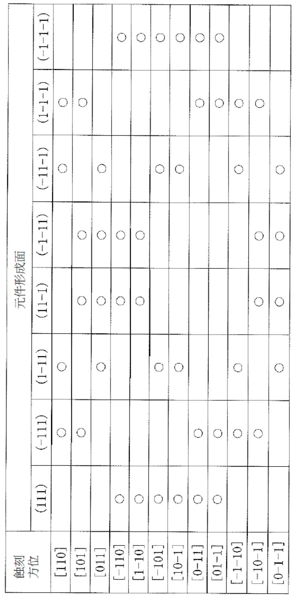
如表1所示,{111}面與<110>方向之組合存在96(=8×12)種。然而,本揭示之<110>方向被限定於與元件形成面即{111}面正交之方向、及與元件形成面平行之方向。即,本揭示之Si{111}基板之元件形成面與對該Si{111}基板進行蝕刻之方位之組合自表1中以○顯示之組合之任一者選擇。As shown in Table 1, there are 96 (=8×12) combinations of {111} plane and <110> direction. However, the <110> direction of the present disclosure is limited to the direction orthogonal to the {111} plane that is the element forming surface, and the direction parallel to the element forming surface. That is, the combination of the element formation surface of the Si{111} substrate of the present disclosure and the orientation of etching the Si{111} substrate is selected from any combination shown by ○ in Table 1.
又,於上述實施形態中,已例示使用Si{111}基板,且蝕刻向X軸方向行進,另一方面,不向Y軸方向及Z軸方向行進之情形。然而,本揭示不限定於此,只要於X軸方向及Y軸方向之兩者,或者X軸方向或Y軸方向之任一者具有蝕刻行進方位即可。又,於Si{111}基板,例如如圖27所示,亦包含以相對於<112>方向有傾斜角之方式加工基板表面之基板之情形。於傾斜角為19.47°以下之情形時,即使為具有傾斜角之基板之情形,亦可保證相對於<111>方向,即具有3條Si背鍵之方向之蝕刻率,<110>方向,即具有1條Si背鍵之方向之蝕刻率充分高之關係。若傾斜角變大則步驟數變多,微差密度變高,故較佳為5°以下。另,圖27之例中,雖列舉基板表面於<112>方向有傾斜角之情形,但亦可為於<110>方向有傾斜角之情形,傾斜角之方向可為任意。又,Si面方位可使用X射線繞射法、電子線繞射法、電子線背向散射繞射法等解析。由於Si背鍵數為由Si之結晶構造決定者,故可藉由解析Si面方位來解析矽背鍵數。In addition, in the above-mentioned embodiment, a case where a Si{111} substrate is used and the etching proceeds in the X-axis direction, on the other hand, does not proceed in the Y-axis direction and the Z-axis direction. However, the present disclosure is not limited to this, as long as it has an etching direction in both the X-axis direction and the Y-axis direction, or either the X-axis direction or the Y-axis direction. In addition, the Si{111} substrate, for example, as shown in FIG. 27, also includes the case where the substrate surface is processed with an inclination angle with respect to the <112> direction. When the inclination angle is below 19.47°, even in the case of a substrate with an inclination angle, the etching rate relative to the <111> direction, that is, the direction with 3 Si back bonds, is guaranteed, and the <110> direction is There is a relationship that the etching rate in the direction of one Si back bond is sufficiently high. As the inclination angle becomes larger, the number of steps becomes larger and the differential density becomes higher, so it is preferably 5° or less. In addition, in the example of FIG. 27, although the case where the substrate surface has an inclination angle in the <112> direction is illustrated, it may also be the case in which there is an inclination angle in the <110> direction, and the direction of the inclination angle can be arbitrary. In addition, the Si plane orientation can be analyzed using X-ray diffraction method, electron wire diffraction method, electron wire backscatter diffraction method, etc. Since the number of Si back bonds is determined by the crystalline structure of Si, the number of Si back bonds can be analyzed by analyzing the Si plane orientation.
<構成之組合例> 另,本技術亦可採取如下之構成。 (1) 一種攝像元件,其具備: 半導體基板,其供形成對照射之光進行光電轉換之光電轉換部; 溝槽部,其自上述半導體基板之受光面側,設置於複數個上述光電轉換部彼此之間;及 突起部,其於上述溝槽部之一部分,至少設置有以上述溝槽部之間隔變寬之方式相對於上述溝槽部之側面傾斜之傾斜面。 (2) 如上述(1)記載之攝像元件,其中 上述突起部由沿著構成上述半導體基板之結晶之特定面方位的上述傾斜面構成。 (3) 如上述(1)或(2)記載之攝像元件,其中 上述突起部設置於上述溝槽部之前端。 (4) 如上述(1)至(3)中任一項記載之攝像元件,其中 上述突起部設置於上述半導體基板之受光面至上述溝槽部之前端間之中段。 (5) 如上述(1)至(4)中任一項記載之攝像元件,其中 上述突起部設置於上述半導體基板之受光面至上述溝槽部之前端間之複數個部位。 (6) 如上述(1)至(5)中任一項記載之攝像元件,其中 於上述溝槽部及上述突起部埋入抑制光之透過之材料。 (7) 如上述(6)記載之攝像元件,其中 埋入至上述突起部中較上述溝槽部之側面更朝側面方向突出之突出部的第1材料、與埋入至上述突出部以外之上述溝槽部之內部的第2材料之特性各不相同。 (8) 如上述(7)記載之攝像元件,其中 上述第1材料對光之吸收係數高於上述第2材料,且 上述第2材料對光之反射率高於上述第1材料。 (9) 如上述(1)至(8)中任一項記載之攝像元件,其中 上述半導體基板係將第1方向作為厚度方向且沿著與上述第1方向正交之水平面擴展之具有以面指數{111}表示之第1結晶面的Si{111}基板,且 上述突起部之上述傾斜面包含相對於上述第1方向傾斜且沿著以面指數{111}表示之上述Si{111}基板之結晶面之面。 (10) 一種攝像元件,其具有: Si基板,其將第1方向作為厚度方向且沿著與上述第1方向正交之水平面擴展; 光電轉換部,其設置於上述Si基板,藉由光電轉換產生對應於受光量之電荷;及 突起部,其在設置於複數個上述光電轉換部彼此間之溝槽部之一部分,至少設置有以上述溝槽部之間隔變寬之方式相對於上述溝槽部之側面傾斜之傾斜面;且 上述突起部包含相對於上述第1方向傾斜且沿著具有3條Si背鍵之第2結晶面之面。 (11) 一種製造方法,其包含: 由製造攝像元件之製造裝置 自供形成對照射之光進行光電轉換之光電轉換部的半導體基板之受光面側,刻入設置於複數個上述光電轉換部彼此之間的溝槽部;及 形成:於上述溝槽部之一部分,至少設置有以使上述溝槽部之間隔變寬之方式相對於上述溝槽部之側面傾斜之傾斜面。 (12) 一種電子機器,其具備攝像元件,該攝像元件具有: 半導體基板,其供形成對照射之光進行光電轉換之光電轉換部; 溝槽部,其自上述半導體基板之受光面側,設置於複數個上述光電轉換部彼此之間;及 突起部,其於上述溝槽部之一部分,至少設置有以上述溝槽部之間隔變寬之方式相對於上述溝槽部之側面傾斜之傾斜面。 (13) 如上述(11)記載之製造方法,其中 上述突起部藉由使用鹼性藥液之矽面方位選擇蝕刻形成。<Combination example> In addition, this technology can also adopt the following configurations. (1) An image pickup element including: A semiconductor substrate for forming a photoelectric conversion part for photoelectric conversion of irradiated light; A groove portion, which is provided between the plurality of photoelectric conversion portions from the light receiving surface side of the semiconductor substrate; and The protrusion part is provided with at least a part of the groove part with an inclined surface inclined with respect to the side surface of the groove part so that the interval between the groove parts is widened. (2) The imaging device described in (1) above, wherein The protruding portion is composed of the inclined surface along the specific plane orientation of the crystal constituting the semiconductor substrate. (3) The imaging element described in (1) or (2) above, wherein The protrusion is provided at the front end of the groove. (4) The imaging element described in any one of (1) to (3) above, wherein The protruding portion is provided in the middle section between the light receiving surface of the semiconductor substrate and the front end of the groove portion. (5) The imaging element described in any one of (1) to (4) above, wherein The protrusions are provided at a plurality of locations from the light-receiving surface of the semiconductor substrate to the front end of the groove. (6) The imaging element described in any one of (1) to (5) above, wherein A material that suppresses the transmission of light is buried in the groove portion and the protrusion portion. (7) The imaging element described in (6) above, wherein The properties of the first material embedded in the protruding part that protrudes in the lateral direction from the side of the groove part in the protruding part and the second material embedded in the inside of the groove part other than the protruding part have different characteristics. the same. (8) The imaging element as described in (7) above, wherein The light absorption coefficient of the first material is higher than that of the second material, and The reflectivity of the second material to light is higher than that of the first material. (9) The imaging element described in any one of (1) to (8) above, wherein The semiconductor substrate is a Si{111} substrate having a first crystal plane represented by a face index {111} with the first direction as the thickness direction and extending along a horizontal plane orthogonal to the first direction, and The inclined surface of the protruding portion includes a surface inclined with respect to the first direction and along the crystal plane of the Si{111} substrate represented by the surface index {111}. (10) An imaging element having: Si substrate, which has the first direction as the thickness direction and extends along a horizontal plane orthogonal to the first direction; The photoelectric conversion part, which is arranged on the above Si substrate, generates electric charges corresponding to the amount of light received through photoelectric conversion; and A protruding portion is provided with at least a portion of the groove portion provided between the plurality of the photoelectric conversion portions with an inclined surface inclined with respect to the side surface of the groove portion in such a way that the interval between the groove portions is widened; and The protrusion includes a surface that is inclined with respect to the first direction and is along a second crystal surface having three Si back bonds. (11) A manufacturing method, which includes: Manufacturing device for manufacturing imaging element From the light-receiving surface side of the semiconductor substrate on which the photoelectric conversion portion for photoelectric conversion of the irradiated light is formed, groove portions provided between the plurality of the photoelectric conversion portions are engraved; and Formation: At least a part of the groove portion is provided with an inclined surface that is inclined with respect to the side surface of the groove portion so as to widen the interval between the groove portions. (12) An electronic machine is provided with an imaging element, and the imaging element has: A semiconductor substrate for forming a photoelectric conversion part for photoelectric conversion of irradiated light; A groove portion, which is provided between the plurality of photoelectric conversion portions from the light receiving surface side of the semiconductor substrate; and The protrusion part is provided with at least a part of the groove part with an inclined surface inclined with respect to the side surface of the groove part so that the interval between the groove parts is widened. (13) The manufacturing method described in (11) above, wherein The above-mentioned protrusions are formed by selective etching of the silicon surface orientation using an alkaline chemical solution.
另,本實施形態並非限定於上之述實施形態者,於不脫離本揭示之主旨之範圍內可進行各種變更。又,本說明書中記載之效果僅為例示並非受限定者,亦可為其他效果。In addition, this embodiment is not limited to the above-described embodiment, and various changes can be made without departing from the scope of the present disclosure. In addition, the effects described in this specification are merely illustrative and not limited, and other effects may also be used.
11:半導體基板 11A:半導體基板 11B:半導體基板 11C:半導體基板 11D:半導體基板 12:平坦化膜 12A:平坦化膜 13:濾光片層 14:晶載透鏡層 15:配線層 21:元件分離部 21A:元件分離部 21a:元件分離部 21B:元件分離部 21b:元件分離部 21D:元件分離部 21F:元件分離部 21G:元件分離部 22:溝槽側面 23:平坦部 24:遮光部 25:遮光部 31:元件分離部 31’:元件分離部 31’’:元件分離部 31A:元件分離部 31a:元件分離部 31B:元件分離部 31b:元件分離部 31C:元件分離部 31D:元件分離部 31E:元件分離部 31F:元件分離部 31G:元件分離部 32:溝槽側面 32’:溝槽側面 32’’:溝槽側面 33:突起部 33’:突起部 33’’:突起部 33E:突起部 34:遮光部 35:遮光部 36:遮光部 37:遮光壁 41:傾斜面 42:傾斜面 43:傾斜面 44:傾斜面 51:攝像元件 51-1:攝像元件 51-2:攝像元件 51A-1:攝像元件 51A-2:攝像元件 51B-1:攝像元件 51B-2:攝像元件 51C-1:攝像元件 51C-2:攝像元件 51D-1:攝像元件 51D-2:攝像元件 51E:攝像元件 51F-1:攝像元件 51F-2:攝像元件 51G-1:攝像元件 51G-2:攝像元件 51H-1:攝像元件 51H-2:攝像元件 52:像素 52a:像素 52b:像素 53:彩色濾光片 54:微透鏡 55:內透鏡 61:遮光壁 62:電荷蓄積部 63:開口部 64:FD部 71:元件分離部 73:突起部 81:元件分離部 83:平坦部 101:硬罩 102:溝槽 102-1:溝槽 102-2:溝槽 103:側面 103-1:側面 103-2:側面 104:底面 104-1:底面 104-2:底面 105:側壁 105-1:側壁 105-2:側壁 106:底面 106-1:底面 106-2:底面 107:突出部 107-1:突出部 107-2:突出部 108-1:遮罩 108-2:遮罩 109:突出部 109-1:突出部 110:底面 111:矽面 <111>:方向 112:氮化矽膜 112-1:氮化矽膜 112-2:氮化矽膜 113:硬罩 113-1:硬罩 113-2:硬罩 114:氮化矽膜 115:抗蝕劑 116:氧化矽膜 121:鎢 122:鎢 123:鋁 201:攝像裝置 202:光學系統 203:攝像元件 204:信號處理電路 205:監視器 206:記憶體 B:像素 G:像素 PD:光電二極體 R:像素11: Semiconductor substrate 11A: Semiconductor substrate 11B: Semiconductor substrate 11C: Semiconductor substrate 11D: Semiconductor substrate 12: Flattening film 12A: Flattening film 13: filter layer 14: Crystal mounted lens layer 15: Wiring layer 21: component separation part 21A: component separation part 21a: component separation part 21B: component separation part 21b: component separation part 21D: component separation part 21F: component separation part 21G: component separation part 22: groove side 23: flat part 24: Shading part 25: Shading part 31: component separation part 31’: Component separation part 31’’: Component separation part 31A: component separation part 31a: component separation part 31B: component separation part 31b: component separation part 31C: component separation part 31D: component separation part 31E: component separation part 31F: component separation part 31G: component separation part 32: groove side 32’: groove side 32’’: groove side 33: protrusion 33’: protrusion 33’’: protrusion 33E: protrusion 34: Shading part 35: Shading part 36: Shading part 37: shading wall 41: Inclined surface 42: Inclined surface 43: Inclined surface 44: Inclined surface 51: image sensor 51-1: Imaging element 51-2: Imaging element 51A-1: Imaging element 51A-2: Image sensor 51B-1: Image sensor 51B-2: Image sensor 51C-1: Imaging element 51C-2: Imaging element 51D-1: Imaging element 51D-2: Imaging element 51E: image sensor 51F-1: Camera element 51F-2: Camera element 51G-1: image sensor 51G-2: Camera element 51H-1: Image sensor 51H-2: Image sensor 52: pixels 52a: pixel 52b: pixel 53: Color filter 54: Micro lens 55: inner lens 61: shading wall 62: Charge accumulation section 63: opening 64: FD Department 71: component separation part 73: protrusion 81: component separation part 83: flat part 101: hard cover 102: groove 102-1: groove 102-2: groove 103: side 103-1: side 103-2: side 104: Bottom 104-1: bottom surface 104-2: bottom surface 105: side wall 105-1: side wall 105-2: side wall 106: Bottom 106-1: bottom surface 106-2: bottom surface 107: protrusion 107-1: protrusion 107-2: protrusion 108-1: Mask 108-2: Mask 109: protrusion 109-1: protrusion 110: Bottom 111: Silicon surface <111>: Direction 112: Silicon nitride film 112-1: Silicon nitride film 112-2: Silicon nitride film 113: Hard Cover 113-1: Hard cover 113-2: Hard cover 114: silicon nitride film 115: resist 116: Silicon oxide film 121: Tungsten 122: Tungsten 123: Aluminum 201: Camera 202: optical system 203: Imaging element 204: signal processing circuit 205: Monitor 206: Memory B: pixel G: pixel PD: photodiode R: pixel
圖1A~C係說明應用本技術之攝像元件具備之元件分離部之基本構成例之圖。 圖2A~D係顯示元件分離部之俯視配置例之圖。 圖3A、B係顯示攝像元件之第1構成例之剖視圖。 圖4A、B係顯示攝像元件之第2構成例之剖視圖。 圖5A、B係顯示攝像元件之第3構成例之剖視圖。 圖6A、B係顯示攝像元件之第4構成例之剖視圖。 圖7A、B係顯示元件分離部之變化例之圖。 圖8A、B係顯示攝像元件之第5構成例之剖視圖。 圖9係顯示攝像元件之第6構成例之剖視圖。 圖10係對俯視觀察時之突起部與開口部之關係進行說明之圖。 圖11A、B係顯示攝像元件之第7構成例之剖視圖。 圖12A、B係顯示攝像元件之第8構成例之剖視圖。 圖13A、B係顯示攝像元件之第9構成例之剖視圖。 圖14A~C係顯示元件分離部之俯視配置例之圖。 圖15係對第1製造方法進行說明之圖。 圖16係對第2製造方法進行說明之圖。 圖17係對第3製造方法進行說明之圖。 圖18係對第4製造方法進行說明之圖。 圖19係對第5製造方法進行說明之圖。 圖20係對第5製造方法進行說明之圖。 圖21係對第6製造方法進行說明之圖。 圖22係對第7製造方法進行說明之圖。 圖23係對第8製造方法進行說明之圖。 圖24係顯示攝像裝置之構成例之方塊圖。 圖25係顯示使用影像感測器之使用例之圖。 圖26係說明本揭示之Si基板之結晶面之背鍵之模式圖。 圖27係說明本揭示之Si基板表面之傾斜角之模式圖。1A to 1C are diagrams illustrating examples of the basic configuration of the element separation portion of the imaging element to which the present technology is applied. 2A to 2D are diagrams showing examples of the top-view arrangement of the separation part of the display element. 3A and B are cross-sectional views showing a first configuration example of the imaging element. 4A and B are cross-sectional views showing a second configuration example of the imaging element. 5A and B are cross-sectional views showing a third configuration example of the imaging element. 6A and B are cross-sectional views showing a fourth configuration example of the imaging element. Figures 7A and B are diagrams showing modified examples of component separation parts. 8A and B are cross-sectional views showing a fifth configuration example of the imaging element. Fig. 9 is a cross-sectional view showing a sixth configuration example of the imaging element. Fig. 10 is a diagram explaining the relationship between the protrusion and the opening in a plan view. 11A and B are cross-sectional views showing a seventh configuration example of the imaging element. 12A and B are cross-sectional views showing an eighth configuration example of the imaging element. 13A and B are cross-sectional views showing a ninth configuration example of the imaging element. 14A to C are diagrams showing examples of the top-view arrangement of the device separation portion. Fig. 15 is a diagram illustrating the first manufacturing method. Fig. 16 is a diagram explaining the second manufacturing method. Fig. 17 is a diagram explaining the third manufacturing method. Fig. 18 is a diagram for explaining the fourth manufacturing method. Fig. 19 is a diagram for explaining the fifth manufacturing method. Fig. 20 is a diagram for explaining the fifth manufacturing method. Fig. 21 is a diagram for explaining the sixth manufacturing method. Fig. 22 is a diagram for explaining the seventh manufacturing method. Fig. 23 is a diagram explaining the eighth manufacturing method. Fig. 24 is a block diagram showing a configuration example of the imaging device. Figure 25 is a diagram showing an example of using the image sensor. FIG. 26 is a schematic diagram illustrating the back bond of the crystal surface of the Si substrate of the present disclosure. FIG. 27 is a schematic diagram illustrating the inclination angle of the surface of the Si substrate of the present disclosure.
11:半導體基板 11: Semiconductor substrate
21a:元件分離部 21a: component separation part
21b:元件分離部 21b: component separation part
31:元件分離部 31: component separation part
31a:元件分離部 31a: component separation part
31b:元件分離部 31b: component separation part
32:溝槽側面 32: groove side
33:突起部 33: protrusion
41:傾斜面 41: Inclined surface
42:傾斜面 42: Inclined surface
43:傾斜面 43: Inclined surface
44:傾斜面 44: Inclined surface
<111>:方向 <111>: Direction
Claims (12)
Applications Claiming Priority (2)
| Application Number | Priority Date | Filing Date | Title |
|---|---|---|---|
| JP2018-207880 | 2018-11-05 | ||
| JP2018207880A JP7175159B2 (en) | 2018-11-05 | 2018-11-05 | Imaging device, manufacturing method, and electronic device |
Publications (2)
| Publication Number | Publication Date |
|---|---|
| TW202025471A true TW202025471A (en) | 2020-07-01 |
| TWI852952B TWI852952B (en) | 2024-08-21 |
Family
ID=
Also Published As
| Publication number | Publication date |
|---|---|
| JP7175159B2 (en) | 2022-11-18 |
| EP3879572A1 (en) | 2021-09-15 |
| DE112019005525T5 (en) | 2021-08-19 |
| EP3879572A4 (en) | 2022-01-26 |
| KR20210083261A (en) | 2021-07-06 |
| JP2023010758A (en) | 2023-01-20 |
| CN112970114A (en) | 2021-06-15 |
| JP2020077650A (en) | 2020-05-21 |
| US20220223642A1 (en) | 2022-07-14 |
| WO2020095674A1 (en) | 2020-05-14 |
Similar Documents
| Publication | Publication Date | Title |
|---|---|---|
| WO2020095674A1 (en) | Imaging element, manufacturing method, and electronic device | |
| US20200251514A1 (en) | Solid-state imaging device, manufacturing method thereof, and electronic device | |
| CN108292665B (en) | Solid-state image pickup element, image pickup apparatus, and method of manufacturing solid-state image pickup element | |
| TWI514559B (en) | Solid state imaging device, and method of manufacturing solid state imaging device | |
| KR101683300B1 (en) | Solid-state imaging device, method of manufacturing the same, and electronic apparatus | |
| CN101800233B (en) | Solid-state imaging device, method of manufacturing the same, and electronic apparatus | |
| JP6060851B2 (en) | Method for manufacturing solid-state imaging device | |
| TWI531052B (en) | Method of manufacturing solid-state imaging device | |
| CN103779364A (en) | Method of manufacturing solid-state imaging device and solid-state imaging device | |
| CN110957338A (en) | Solid-state imaging device | |
| JP2009182223A (en) | Back-surface irradiation solid-state imaging element | |
| WO2018083990A1 (en) | Imaging element, imaging device and electronic device | |
| JP2013229446A (en) | Solid-state image sensor and method for manufacturing the same | |
| WO2021251270A1 (en) | Method for manufacturing optical detection device, optical detection device, and electronic device | |
| WO2014049941A1 (en) | Solid-state image pickup device and image pickup device | |
| TWI852952B (en) | Imaging element, manufacturing method, and electronic device | |
| JP2021034405A (en) | Imaging element and imaging apparatus | |
| JP7556008B2 (en) | Photodetector | |
| JP4662966B2 (en) | Imaging device | |
| WO2022123954A1 (en) | Solid-state imaging device, electronic apparatus and solid-state imaging device production method | |
| WO2024185542A1 (en) | Light detection device manufacturing method, and light detection device | |
| JP2017183387A (en) | Circuit board, semiconductor device, imaging device, solid-state imaging element, and method of manufacturing solid-state imaging element, and electronic equipment | |
| JP2024127465A (en) | Method for manufacturing a light detection device and a light detection device | |
| KR20240026136A (en) | Solid-state imaging device and manufacturing method, and electronic device | |
| JP2016131203A (en) | Solid state image pick-up device, manufacturing method and electronic device |