RU2693123C2 - Oled translucent diffusion substrate and method for making such substrate - Google Patents
Oled translucent diffusion substrate and method for making such substrate Download PDFInfo
- Publication number
- RU2693123C2 RU2693123C2 RU2017104776A RU2017104776A RU2693123C2 RU 2693123 C2 RU2693123 C2 RU 2693123C2 RU 2017104776 A RU2017104776 A RU 2017104776A RU 2017104776 A RU2017104776 A RU 2017104776A RU 2693123 C2 RU2693123 C2 RU 2693123C2
- Authority
- RU
- Russia
- Prior art keywords
- layer
- refractive index
- glass
- enamel
- high refractive
- Prior art date
Links
- 239000000758 substrate Substances 0.000 title claims abstract description 87
- 238000000034 method Methods 0.000 title claims abstract description 13
- 238000009792 diffusion process Methods 0.000 title description 3
- 239000011521 glass Substances 0.000 claims abstract description 99
- 210000003298 dental enamel Anatomy 0.000 claims abstract description 56
- 229910044991 metal oxide Inorganic materials 0.000 claims abstract description 41
- 150000004706 metal oxides Chemical class 0.000 claims abstract description 41
- 230000008018 melting Effects 0.000 claims abstract description 16
- 238000002844 melting Methods 0.000 claims abstract description 16
- 239000011248 coating agent Substances 0.000 claims abstract description 14
- 238000000576 coating method Methods 0.000 claims abstract description 14
- 238000000137 annealing Methods 0.000 claims abstract description 13
- 238000004519 manufacturing process Methods 0.000 claims abstract description 6
- 239000000203 mixture Substances 0.000 claims abstract description 6
- 239000010410 layer Substances 0.000 claims description 110
- 229910010413 TiO 2 Inorganic materials 0.000 claims description 11
- 229910015902 Bi 2 O 3 Inorganic materials 0.000 claims description 6
- 229910018072 Al 2 O 3 Inorganic materials 0.000 claims description 4
- 229910005191 Ga 2 O 3 Inorganic materials 0.000 claims description 3
- 229910006404 SnO 2 Inorganic materials 0.000 claims description 3
- GEIAQOFPUVMAGM-UHFFFAOYSA-N ZrO Inorganic materials [Zr]=O GEIAQOFPUVMAGM-UHFFFAOYSA-N 0.000 claims description 3
- 239000002356 single layer Substances 0.000 claims description 3
- 238000000151 deposition Methods 0.000 abstract description 2
- 230000000694 effects Effects 0.000 abstract description 2
- GWEVSGVZZGPLCZ-UHFFFAOYSA-N Titan oxide Chemical compound O=[Ti]=O GWEVSGVZZGPLCZ-UHFFFAOYSA-N 0.000 abstract 2
- MCMNRKCIXSYSNV-UHFFFAOYSA-N Zirconium dioxide Chemical compound O=[Zr]=O MCMNRKCIXSYSNV-UHFFFAOYSA-N 0.000 abstract 2
- WMWLMWRWZQELOS-UHFFFAOYSA-N bismuth(iii) oxide Chemical compound O=[Bi]O[Bi]=O WMWLMWRWZQELOS-UHFFFAOYSA-N 0.000 abstract 2
- ZKATWMILCYLAPD-UHFFFAOYSA-N niobium pentoxide Chemical compound O=[Nb](=O)O[Nb](=O)=O ZKATWMILCYLAPD-UHFFFAOYSA-N 0.000 abstract 2
- XOLBLPGZBRYERU-UHFFFAOYSA-N tin dioxide Chemical compound O=[Sn]=O XOLBLPGZBRYERU-UHFFFAOYSA-N 0.000 abstract 2
- PNEYBMLMFCGWSK-UHFFFAOYSA-N aluminium oxide Inorganic materials [O-2].[O-2].[O-2].[Al+3].[Al+3] PNEYBMLMFCGWSK-UHFFFAOYSA-N 0.000 abstract 1
- 229910052593 corundum Inorganic materials 0.000 abstract 1
- QZQVBEXLDFYHSR-UHFFFAOYSA-N gallium(III) oxide Inorganic materials O=[Ga]O[Ga]=O QZQVBEXLDFYHSR-UHFFFAOYSA-N 0.000 abstract 1
- CJNBYAVZURUTKZ-UHFFFAOYSA-N hafnium(IV) oxide Inorganic materials O=[Hf]=O CJNBYAVZURUTKZ-UHFFFAOYSA-N 0.000 abstract 1
- PJXISJQVUVHSOJ-UHFFFAOYSA-N indium(III) oxide Inorganic materials [O-2].[O-2].[O-2].[In+3].[In+3] PJXISJQVUVHSOJ-UHFFFAOYSA-N 0.000 abstract 1
- 239000000126 substance Substances 0.000 abstract 1
- PBCFLUZVCVVTBY-UHFFFAOYSA-N tantalum pentoxide Inorganic materials O=[Ta](=O)O[Ta](=O)=O PBCFLUZVCVVTBY-UHFFFAOYSA-N 0.000 abstract 1
- ZNOKGRXACCSDPY-UHFFFAOYSA-N tungsten(VI) oxide Inorganic materials O=[W](=O)=O ZNOKGRXACCSDPY-UHFFFAOYSA-N 0.000 abstract 1
- 229910001845 yogo sapphire Inorganic materials 0.000 abstract 1
- 239000012044 organic layer Substances 0.000 description 8
- 239000002245 particle Substances 0.000 description 7
- 239000002253 acid Substances 0.000 description 6
- 238000000149 argon plasma sintering Methods 0.000 description 6
- 230000015572 biosynthetic process Effects 0.000 description 6
- 238000000605 extraction Methods 0.000 description 6
- 239000003960 organic solvent Substances 0.000 description 4
- 239000007787 solid Substances 0.000 description 4
- 239000001856 Ethyl cellulose Substances 0.000 description 3
- ZZSNKZQZMQGXPY-UHFFFAOYSA-N Ethyl cellulose Chemical compound CCOCC1OC(OC)C(OCC)C(OCC)C1OC1C(O)C(O)C(OC)C(CO)O1 ZZSNKZQZMQGXPY-UHFFFAOYSA-N 0.000 description 3
- VEUACKUBDLVUAC-UHFFFAOYSA-N [Na].[Ca] Chemical compound [Na].[Ca] VEUACKUBDLVUAC-UHFFFAOYSA-N 0.000 description 3
- 239000013078 crystal Substances 0.000 description 3
- 239000000975 dye Substances 0.000 description 3
- 229920001249 ethyl cellulose Polymers 0.000 description 3
- 235000019325 ethyl cellulose Nutrition 0.000 description 3
- 238000010438 heat treatment Methods 0.000 description 3
- 238000001755 magnetron sputter deposition Methods 0.000 description 3
- 239000013642 negative control Substances 0.000 description 3
- 239000002904 solvent Substances 0.000 description 3
- XLYOFNOQVPJJNP-UHFFFAOYSA-N water Substances O XLYOFNOQVPJJNP-UHFFFAOYSA-N 0.000 description 3
- 229910004298 SiO 2 Inorganic materials 0.000 description 2
- -1 TiO 2 Chemical class 0.000 description 2
- 238000000231 atomic layer deposition Methods 0.000 description 2
- 238000005056 compaction Methods 0.000 description 2
- 239000012530 fluid Substances 0.000 description 2
- AMGQUBHHOARCQH-UHFFFAOYSA-N indium;oxotin Chemical compound [In].[Sn]=O AMGQUBHHOARCQH-UHFFFAOYSA-N 0.000 description 2
- 239000000047 product Substances 0.000 description 2
- 230000005855 radiation Effects 0.000 description 2
- 230000000630 rising effect Effects 0.000 description 2
- 238000007650 screen-printing Methods 0.000 description 2
- 238000004458 analytical method Methods 0.000 description 1
- 230000004888 barrier function Effects 0.000 description 1
- 230000009286 beneficial effect Effects 0.000 description 1
- 239000011230 binding agent Substances 0.000 description 1
- 239000007795 chemical reaction product Substances 0.000 description 1
- 150000001875 compounds Chemical class 0.000 description 1
- 229910021488 crystalline silicon dioxide Inorganic materials 0.000 description 1
- 230000006378 damage Effects 0.000 description 1
- 230000007547 defect Effects 0.000 description 1
- 230000008021 deposition Effects 0.000 description 1
- 238000010586 diagram Methods 0.000 description 1
- 239000003085 diluting agent Substances 0.000 description 1
- 238000001035 drying Methods 0.000 description 1
- 239000002320 enamel (paints) Substances 0.000 description 1
- 238000005530 etching Methods 0.000 description 1
- 230000008020 evaporation Effects 0.000 description 1
- 238000001704 evaporation Methods 0.000 description 1
- 238000001125 extrusion Methods 0.000 description 1
- 239000005357 flat glass Substances 0.000 description 1
- 239000003365 glass fiber Substances 0.000 description 1
- 238000007496 glass forming Methods 0.000 description 1
- 238000000227 grinding Methods 0.000 description 1
- 238000009499 grossing Methods 0.000 description 1
- 230000003993 interaction Effects 0.000 description 1
- 238000003475 lamination Methods 0.000 description 1
- 239000007788 liquid Substances 0.000 description 1
- 239000006060 molten glass Substances 0.000 description 1
- 238000012806 monitoring device Methods 0.000 description 1
- 239000005306 natural glass Substances 0.000 description 1
- 230000005693 optoelectronics Effects 0.000 description 1
- 229920000620 organic polymer Polymers 0.000 description 1
- 229920000642 polymer Polymers 0.000 description 1
- 239000000843 powder Substances 0.000 description 1
- 239000002243 precursor Substances 0.000 description 1
- 238000002360 preparation method Methods 0.000 description 1
- 239000011241 protective layer Substances 0.000 description 1
- 239000011734 sodium Substances 0.000 description 1
- 238000007711 solidification Methods 0.000 description 1
- 230000008023 solidification Effects 0.000 description 1
- 238000010561 standard procedure Methods 0.000 description 1
- 230000003746 surface roughness Effects 0.000 description 1
- 238000002834 transmittance Methods 0.000 description 1
Images
Classifications
-
- G—PHYSICS
- G02—OPTICS
- G02B—OPTICAL ELEMENTS, SYSTEMS OR APPARATUS
- G02B5/00—Optical elements other than lenses
- G02B5/02—Diffusing elements; Afocal elements
- G02B5/0268—Diffusing elements; Afocal elements characterized by the fabrication or manufacturing method
-
- C—CHEMISTRY; METALLURGY
- C03—GLASS; MINERAL OR SLAG WOOL
- C03C—CHEMICAL COMPOSITION OF GLASSES, GLAZES OR VITREOUS ENAMELS; SURFACE TREATMENT OF GLASS; SURFACE TREATMENT OF FIBRES OR FILAMENTS MADE FROM GLASS, MINERALS OR SLAGS; JOINING GLASS TO GLASS OR OTHER MATERIALS
- C03C17/00—Surface treatment of glass, not in the form of fibres or filaments, by coating
- C03C17/006—Surface treatment of glass, not in the form of fibres or filaments, by coating with materials of composite character
- C03C17/007—Surface treatment of glass, not in the form of fibres or filaments, by coating with materials of composite character containing a dispersed phase, e.g. particles, fibres or flakes, in a continuous phase
-
- C—CHEMISTRY; METALLURGY
- C03—GLASS; MINERAL OR SLAG WOOL
- C03C—CHEMICAL COMPOSITION OF GLASSES, GLAZES OR VITREOUS ENAMELS; SURFACE TREATMENT OF GLASS; SURFACE TREATMENT OF FIBRES OR FILAMENTS MADE FROM GLASS, MINERALS OR SLAGS; JOINING GLASS TO GLASS OR OTHER MATERIALS
- C03C17/00—Surface treatment of glass, not in the form of fibres or filaments, by coating
- C03C17/02—Surface treatment of glass, not in the form of fibres or filaments, by coating with glass
- C03C17/04—Surface treatment of glass, not in the form of fibres or filaments, by coating with glass by fritting glass powder
-
- C—CHEMISTRY; METALLURGY
- C03—GLASS; MINERAL OR SLAG WOOL
- C03C—CHEMICAL COMPOSITION OF GLASSES, GLAZES OR VITREOUS ENAMELS; SURFACE TREATMENT OF GLASS; SURFACE TREATMENT OF FIBRES OR FILAMENTS MADE FROM GLASS, MINERALS OR SLAGS; JOINING GLASS TO GLASS OR OTHER MATERIALS
- C03C17/00—Surface treatment of glass, not in the form of fibres or filaments, by coating
- C03C17/22—Surface treatment of glass, not in the form of fibres or filaments, by coating with other inorganic material
- C03C17/23—Oxides
-
- C—CHEMISTRY; METALLURGY
- C03—GLASS; MINERAL OR SLAG WOOL
- C03C—CHEMICAL COMPOSITION OF GLASSES, GLAZES OR VITREOUS ENAMELS; SURFACE TREATMENT OF GLASS; SURFACE TREATMENT OF FIBRES OR FILAMENTS MADE FROM GLASS, MINERALS OR SLAGS; JOINING GLASS TO GLASS OR OTHER MATERIALS
- C03C17/00—Surface treatment of glass, not in the form of fibres or filaments, by coating
- C03C17/34—Surface treatment of glass, not in the form of fibres or filaments, by coating with at least two coatings having different compositions
- C03C17/3411—Surface treatment of glass, not in the form of fibres or filaments, by coating with at least two coatings having different compositions with at least two coatings of inorganic materials
- C03C17/3417—Surface treatment of glass, not in the form of fibres or filaments, by coating with at least two coatings having different compositions with at least two coatings of inorganic materials all coatings being oxide coatings
-
- C—CHEMISTRY; METALLURGY
- C03—GLASS; MINERAL OR SLAG WOOL
- C03C—CHEMICAL COMPOSITION OF GLASSES, GLAZES OR VITREOUS ENAMELS; SURFACE TREATMENT OF GLASS; SURFACE TREATMENT OF FIBRES OR FILAMENTS MADE FROM GLASS, MINERALS OR SLAGS; JOINING GLASS TO GLASS OR OTHER MATERIALS
- C03C17/00—Surface treatment of glass, not in the form of fibres or filaments, by coating
- C03C17/34—Surface treatment of glass, not in the form of fibres or filaments, by coating with at least two coatings having different compositions
- C03C17/36—Surface treatment of glass, not in the form of fibres or filaments, by coating with at least two coatings having different compositions at least one coating being a metal
- C03C17/3602—Surface treatment of glass, not in the form of fibres or filaments, by coating with at least two coatings having different compositions at least one coating being a metal the metal being present as a layer
- C03C17/3657—Surface treatment of glass, not in the form of fibres or filaments, by coating with at least two coatings having different compositions at least one coating being a metal the metal being present as a layer the multilayer coating having optical properties
-
- C—CHEMISTRY; METALLURGY
- C03—GLASS; MINERAL OR SLAG WOOL
- C03C—CHEMICAL COMPOSITION OF GLASSES, GLAZES OR VITREOUS ENAMELS; SURFACE TREATMENT OF GLASS; SURFACE TREATMENT OF FIBRES OR FILAMENTS MADE FROM GLASS, MINERALS OR SLAGS; JOINING GLASS TO GLASS OR OTHER MATERIALS
- C03C8/00—Enamels; Glazes; Fusion seal compositions being frit compositions having non-frit additions
- C03C8/02—Frit compositions, i.e. in a powdered or comminuted form
-
- G—PHYSICS
- G02—OPTICS
- G02B—OPTICAL ELEMENTS, SYSTEMS OR APPARATUS
- G02B5/00—Optical elements other than lenses
- G02B5/02—Diffusing elements; Afocal elements
- G02B5/0205—Diffusing elements; Afocal elements characterised by the diffusing properties
- G02B5/0236—Diffusing elements; Afocal elements characterised by the diffusing properties the diffusion taking place within the volume of the element
- G02B5/0247—Diffusing elements; Afocal elements characterised by the diffusing properties the diffusion taking place within the volume of the element by means of voids or pores
-
- G—PHYSICS
- G02—OPTICS
- G02B—OPTICAL ELEMENTS, SYSTEMS OR APPARATUS
- G02B5/00—Optical elements other than lenses
- G02B5/02—Diffusing elements; Afocal elements
- G02B5/0273—Diffusing elements; Afocal elements characterized by the use
- G02B5/0278—Diffusing elements; Afocal elements characterized by the use used in transmission
-
- H—ELECTRICITY
- H05—ELECTRIC TECHNIQUES NOT OTHERWISE PROVIDED FOR
- H05B—ELECTRIC HEATING; ELECTRIC LIGHT SOURCES NOT OTHERWISE PROVIDED FOR; CIRCUIT ARRANGEMENTS FOR ELECTRIC LIGHT SOURCES, IN GENERAL
- H05B33/00—Electroluminescent light sources
- H05B33/02—Details
-
- H—ELECTRICITY
- H05—ELECTRIC TECHNIQUES NOT OTHERWISE PROVIDED FOR
- H05B—ELECTRIC HEATING; ELECTRIC LIGHT SOURCES NOT OTHERWISE PROVIDED FOR; CIRCUIT ARRANGEMENTS FOR ELECTRIC LIGHT SOURCES, IN GENERAL
- H05B33/00—Electroluminescent light sources
- H05B33/10—Apparatus or processes specially adapted to the manufacture of electroluminescent light sources
-
- H—ELECTRICITY
- H05—ELECTRIC TECHNIQUES NOT OTHERWISE PROVIDED FOR
- H05B—ELECTRIC HEATING; ELECTRIC LIGHT SOURCES NOT OTHERWISE PROVIDED FOR; CIRCUIT ARRANGEMENTS FOR ELECTRIC LIGHT SOURCES, IN GENERAL
- H05B33/00—Electroluminescent light sources
- H05B33/12—Light sources with substantially two-dimensional radiating surfaces
- H05B33/22—Light sources with substantially two-dimensional radiating surfaces characterised by the chemical or physical composition or the arrangement of auxiliary dielectric or reflective layers
-
- H—ELECTRICITY
- H10—SEMICONDUCTOR DEVICES; ELECTRIC SOLID-STATE DEVICES NOT OTHERWISE PROVIDED FOR
- H10K—ORGANIC ELECTRIC SOLID-STATE DEVICES
- H10K50/00—Organic light-emitting devices
- H10K50/80—Constructional details
- H10K50/85—Arrangements for extracting light from the devices
- H10K50/854—Arrangements for extracting light from the devices comprising scattering means
-
- H—ELECTRICITY
- H10—SEMICONDUCTOR DEVICES; ELECTRIC SOLID-STATE DEVICES NOT OTHERWISE PROVIDED FOR
- H10K—ORGANIC ELECTRIC SOLID-STATE DEVICES
- H10K77/00—Constructional details of devices covered by this subclass and not covered by groups H10K10/80, H10K30/80, H10K50/80 or H10K59/80
- H10K77/10—Substrates, e.g. flexible substrates
-
- C—CHEMISTRY; METALLURGY
- C03—GLASS; MINERAL OR SLAG WOOL
- C03C—CHEMICAL COMPOSITION OF GLASSES, GLAZES OR VITREOUS ENAMELS; SURFACE TREATMENT OF GLASS; SURFACE TREATMENT OF FIBRES OR FILAMENTS MADE FROM GLASS, MINERALS OR SLAGS; JOINING GLASS TO GLASS OR OTHER MATERIALS
- C03C2217/00—Coatings on glass
- C03C2217/40—Coatings comprising at least one inhomogeneous layer
- C03C2217/43—Coatings comprising at least one inhomogeneous layer consisting of a dispersed phase in a continuous phase
- C03C2217/44—Coatings comprising at least one inhomogeneous layer consisting of a dispersed phase in a continuous phase characterized by the composition of the continuous phase
- C03C2217/45—Inorganic continuous phases
- C03C2217/452—Glass
-
- C—CHEMISTRY; METALLURGY
- C03—GLASS; MINERAL OR SLAG WOOL
- C03C—CHEMICAL COMPOSITION OF GLASSES, GLAZES OR VITREOUS ENAMELS; SURFACE TREATMENT OF GLASS; SURFACE TREATMENT OF FIBRES OR FILAMENTS MADE FROM GLASS, MINERALS OR SLAGS; JOINING GLASS TO GLASS OR OTHER MATERIALS
- C03C2217/00—Coatings on glass
- C03C2217/40—Coatings comprising at least one inhomogeneous layer
- C03C2217/43—Coatings comprising at least one inhomogeneous layer consisting of a dispersed phase in a continuous phase
- C03C2217/46—Coatings comprising at least one inhomogeneous layer consisting of a dispersed phase in a continuous phase characterized by the dispersed phase
- C03C2217/48—Coatings comprising at least one inhomogeneous layer consisting of a dispersed phase in a continuous phase characterized by the dispersed phase having a specific function
-
- C—CHEMISTRY; METALLURGY
- C03—GLASS; MINERAL OR SLAG WOOL
- C03C—CHEMICAL COMPOSITION OF GLASSES, GLAZES OR VITREOUS ENAMELS; SURFACE TREATMENT OF GLASS; SURFACE TREATMENT OF FIBRES OR FILAMENTS MADE FROM GLASS, MINERALS OR SLAGS; JOINING GLASS TO GLASS OR OTHER MATERIALS
- C03C2217/00—Coatings on glass
- C03C2217/70—Properties of coatings
- C03C2217/73—Anti-reflective coatings with specific characteristics
- C03C2217/734—Anti-reflective coatings with specific characteristics comprising an alternation of high and low refractive indexes
-
- C—CHEMISTRY; METALLURGY
- C03—GLASS; MINERAL OR SLAG WOOL
- C03C—CHEMICAL COMPOSITION OF GLASSES, GLAZES OR VITREOUS ENAMELS; SURFACE TREATMENT OF GLASS; SURFACE TREATMENT OF FIBRES OR FILAMENTS MADE FROM GLASS, MINERALS OR SLAGS; JOINING GLASS TO GLASS OR OTHER MATERIALS
- C03C2217/00—Coatings on glass
- C03C2217/90—Other aspects of coatings
- C03C2217/91—Coatings containing at least one layer having a composition gradient through its thickness
-
- C—CHEMISTRY; METALLURGY
- C03—GLASS; MINERAL OR SLAG WOOL
- C03C—CHEMICAL COMPOSITION OF GLASSES, GLAZES OR VITREOUS ENAMELS; SURFACE TREATMENT OF GLASS; SURFACE TREATMENT OF FIBRES OR FILAMENTS MADE FROM GLASS, MINERALS OR SLAGS; JOINING GLASS TO GLASS OR OTHER MATERIALS
- C03C2217/00—Coatings on glass
- C03C2217/90—Other aspects of coatings
- C03C2217/94—Transparent conductive oxide layers [TCO] being part of a multilayer coating
- C03C2217/948—Layers comprising indium tin oxide [ITO]
-
- H—ELECTRICITY
- H10—SEMICONDUCTOR DEVICES; ELECTRIC SOLID-STATE DEVICES NOT OTHERWISE PROVIDED FOR
- H10K—ORGANIC ELECTRIC SOLID-STATE DEVICES
- H10K2102/00—Constructional details relating to the organic devices covered by this subclass
-
- Y—GENERAL TAGGING OF NEW TECHNOLOGICAL DEVELOPMENTS; GENERAL TAGGING OF CROSS-SECTIONAL TECHNOLOGIES SPANNING OVER SEVERAL SECTIONS OF THE IPC; TECHNICAL SUBJECTS COVERED BY FORMER USPC CROSS-REFERENCE ART COLLECTIONS [XRACs] AND DIGESTS
- Y02—TECHNOLOGIES OR APPLICATIONS FOR MITIGATION OR ADAPTATION AGAINST CLIMATE CHANGE
- Y02E—REDUCTION OF GREENHOUSE GAS [GHG] EMISSIONS, RELATED TO ENERGY GENERATION, TRANSMISSION OR DISTRIBUTION
- Y02E10/00—Energy generation through renewable energy sources
- Y02E10/50—Photovoltaic [PV] energy
- Y02E10/549—Organic PV cells
Landscapes
- Chemical & Material Sciences (AREA)
- Engineering & Computer Science (AREA)
- Chemical Kinetics & Catalysis (AREA)
- General Chemical & Material Sciences (AREA)
- Geochemistry & Mineralogy (AREA)
- Materials Engineering (AREA)
- Organic Chemistry (AREA)
- Life Sciences & Earth Sciences (AREA)
- Physics & Mathematics (AREA)
- Optics & Photonics (AREA)
- Manufacturing & Machinery (AREA)
- Dispersion Chemistry (AREA)
- Composite Materials (AREA)
- General Physics & Mathematics (AREA)
- Glass Compositions (AREA)
- Electroluminescent Light Sources (AREA)
- Laminated Bodies (AREA)
- Surface Treatment Of Glass (AREA)
Abstract
Description
Настоящее изобретение выведено для создания нового способа изготовления просвечивающих, светорассеивающих стеклянных подложек для органических светоизлучающих диодов (ОСИД) и для подложек, получаемых таким способом.The present invention has been developed to create a new method of manufacturing translucent, light-scattering glass substrates for organic light-emitting diodes (OLEDs) and for substrates obtained in this way.
ОСИД представляют собой оптоэлектронные элементы, содержащие пакет органических слоев с флуоресцентными или фосфоресцентными красителями, помещенными между двумя электродами, по меньшей мере, один из которых является просвечивающим. При приложении напряжения к электродам, электроны, инжектированные из катода, и дырки, инжектированные из анода, рекомбинируют в органических слоях, приводя к испусканию света из флуоресцентных/фосфоресцентных слоев.Acid are optoelectronic elements containing a package of organic layers with fluorescent or phosphorescent dyes placed between two electrodes, at least one of which is translucent. When a voltage is applied to the electrodes, electrons injected from the cathode and holes injected from the anode recombine in the organic layers, leading to the emission of light from the fluorescent / phosphorescent layers.
Обычно известно, что выведение света из стандартных ОСИД, бывает достаточно слабым, и большая часть света захватывается за счет полного внутреннего отражения в органических слоях с высоким показателем преломления и в прозрачных проводящих слоях (transparent conductive layers, TCL). Полное внутреннее отражение происходит не только на границе между TCL с высоким показателем преломления и нижележащей стеклянной подложкой (с показателем преломления примерно 1,5), но также и на границе между стеклом и воздухом.It is usually known that the removal of light from standard acid is quite weak, and most of the light is captured by total internal reflection in organic layers with a high refractive index and transparent conductive layers (TCL). Total internal reflection occurs not only at the border between TCL with a high refractive index and the underlying glass substrate (with a refractive index of about 1.5), but also at the border between glass and air.
Согласно оценкам в стандартных ОСИД, не содержащих никаких дополнительных световыделяющих слоев, примерно 60% света, испускаемого из органических слоев, захватывается на границе TCL/стекло, дополнительная доля 20% захватывается на границе поверхность стекла/воздух и лишь примерно 20% испускается из ОСИД в воздух.According to estimates, in standard OLEDs that do not contain any additional light-emitting layers, approximately 60% of the light emitted from the organic layers is captured at the TCL / glass interface, an additional 20% is captured at the surface / glass interface and only about 20% is emitted from the OLED in air.
Известно снижение этого захвата света посредством светорассеивающего слоя, расположенного между TCL и стеклянной подложкой. Такие светорассеивающие слои имеют прозрачную кристаллическую структуру, с высоким показателем преломления, близким к показателю преломления TCL, и содержат множество светорассеивающих элементов, обладающих показателем преломления, отличным от показателя преломления кристаллической структуры. Такие кристаллические структуры с высоким показателем преломления обычно получают путем плавления стеклофритты с высоким показателем преломления, с получением, таким образом, тонких слоев эмали с высоким показателем преломления на стеклянных подложках с низким показателем преломления. Светорассеивающие элементы могут представлять собой твердые частицы, добавленные к стеклофритте до этапа плавления, кристаллы, образованные в ходе этапа плавления, или пузырьки воздуха, образованные в ходе этапа плавления.It is known to reduce this light trapping by means of a light scattering layer located between the TCL and the glass substrate. Such light-scattering layers have a transparent crystal structure, with a high refractive index, close to the TCL refractive index, and contain many light-scattering elements that have a refractive index that is different from the refractive index of the crystal structure. Such crystalline structures with a high refractive index are usually obtained by melting glass refrites with a high refractive index, thus obtaining thin enamel layers with a high refractive index on glass substrates with a low refractive index. The light-scattering elements may be solids added to glassfritte prior to the melting step, crystals formed during the melting step, or air bubbles formed during the melting step.
Также известно повышение выхода света за счет текстурирования граничной поверхности, т.е., создания рельефа на границе раздела между стеклом и слоями ОСИД с высоким показателем преломления, например, путем травления или шлифовки прозрачной подложки с низким показателем преломления, до нанесения и расплавления стеклофритты с высоким показателем преломления.It is also known to increase light output by texturing the boundary surface, i.e., creating a relief at the interface between glass and high refractive index acid layers, for example, by etching or grinding a transparent substrate with a low refractive index, before applying and melting the glass frit with high refractive index.
Оба из этих средств выведения света обычно называются «слоями внутреннего выведения света» (internal extraction layers, IEL), поскольку они расположены между подложкой ОСИД и TCL.Both of these light-emitting means are commonly referred to as “internal extraction layers, IEL), since they are located between the OLED substrate and the TCL.
Слои внешнего выведения света (external extraction layers, EEL), также общеизвестные из уровня техники, работают аналогичным образом, но расположены на границе стекло/воздух.The external light removal layers (external layers, EEL), also well known in the art, work in a similar way, but are located on the glass / air interface.
Настоящее изобретение относится к области слоев внутреннего выведения света (internal extraction layers, IEL), обладающих прозрачной структурой с высоким показателем преломления, содержащих пузырьки воздуха в качестве диффузионных элементов с низким показателем преломления. Такой IEL со светорассеивающими пузырьками воздуха является выгодным, по сравнению с IEL с твердыми частицами, из-за отсутствия какого-либо риска появления крупных частиц, выступающих из структуры и порождающих короткое замыкание, и/или внутриэлектродные токи утечки в конечном продукте ОСИД.The present invention relates to the field of layers of internal light extraction (IEL), having a transparent structure with a high refractive index, containing air bubbles as diffusion elements with a low refractive index. Such an IEL with light-scattering air bubbles is advantageous, compared to IEL with solid particles, due to the absence of any risk of the appearance of large particles protruding from the structure and generating a short circuit, and / or intra-electrode leakage currents in the final acid product.
Однако, несмотря на отсутствие трвердых частиц, становится затруднительным получение диффузионных эмалей с идеальным качеством поверхности за счет простого плавления стеклофритты с высокими показателями преломления на стеклянных подложках с низкими показателями преломления. В действительности, пузырьки воздуха, образованные и захваченные в плавящейся структуре в ходе этапа плавления, поднимаются к поверхности, где они лопаются и сглаживаются. Однако открытые или частично открытые пузырьки воздуха, отвердевшие на поверхности IEL до полного выравнивания, создают кратерообразные неровности поверхности, которые могут иметь достаточно острые кромки и могут привести к токам утечки внутри электрода и к точечным отверстиям в конечном ОСИД.However, despite the absence of solid particles, it becomes difficult to obtain diffusion enamels with perfect surface quality due to simple melting of glass frits with high refractive indices on glass substrates with low refractive indices. In fact, air bubbles formed and trapped in a melting structure during the melting stage rise to the surface, where they burst and flatten. However, open or partially open air bubbles that have hardened on the IEL surface before full alignment create crater-like surface irregularities that can have sharp edges and can lead to leakage currents inside the electrode and pinholes in the final acid.
В EP 2 178 343 B1 раскрыты просвечивающие стеклянные подложки для ОСИД со слоем внутреннего выведения света (рассеивающим слоем), содержащим стеклянную структуру с высоким показателем преломления и рассеивающие элементы с использованием воздушных пузырьков. Согласно этому документу на поверхности рассеивающего слоя отсутствуют поверхностные дефекты, образованные из-за кратеров, вызванных открытыми пузырьками воздуха (см. [0026]-[0028] и Фиг. 55). Однако, тщательный анализ данного документа и, в частности, [0202] показывает, что этот результат просто является артефактом, вызванным ненадлежащим способом подсчета рассеивающих элементов в нижних слоях поверхности.
Заявитель недавно подал Южнокорейскую патентную заявку № 10-2013-0084314 (17 июля 2013 г.), не опубликованную на дату подачи настоящей заявки, раскрывающую многослойную подложку для светоизлучающего устройства с системой соединенных между собой пустот, расположенных на границе раздела между стеклянной подложкой с низким показателем преломления и эмалью с высоким показателем преломления. Такой рассеивающий слой обладает очень высоким качеством поверхности с плотностью открытых пузырьков менее 0,1/см2, но страдает от неудобства, состоящего в том, что вода или другие текучие среды, входящие в контакт с кромками многослойной подложки, могут просачиваться через соединенные между собой пустоты по широким областям слоистого изделия, и через точечные отверстия, в пакет органических слоев с флуоресцентными или фосфоресцентными красителями, приводя к разрушению упомянутых слоев.The applicant recently filed the South Korean patent application No. 10-2013-0084314 (July 17, 2013), unpublished on the filing date of this application, revealing a multilayer substrate for a light-emitting device with a system of interconnected voids located at the interface between the glass substrate with a low refractive index and high refractive index enamel. Such a scattering layer has a very high surface quality with an open bubble density of less than 0.1 / cm 2 , but suffers from the inconvenience that water or other fluids that come into contact with the edges of the multilayer substrate can seep through interconnected voids over wide areas of the layered product, and through dotted holes, into a package of organic layers with fluorescent or phosphorescent dyes, leading to the destruction of the layers mentioned.
Поэтому, представляется выгодным обеспечение многослойной подложки для ОСИД, аналогичной многослойной подложке ОСИД, описанной в Южнокорейской заявке № 10-2013-0084314, поданной 17 июля 2013 г. от имени компании Saint-Gobain Glass, Франция, где система взаимно соединенных пустот на граничном слое эмаль/стеклянная подложка с высоким показателем преломления заменена несколькими отдельными пузырьками воздуха, не соединенными друг с другом и прикрепляющимися к упомянутой границе раздела, как правило, без подъема к поверхности плавящейся стеклофритты с высоким показателем преломления.Therefore, it seems beneficial to provide a multilayer substrate for OLED, similar to the OLED multilayer substrate described in the South Korean application No. 10-2013-0084314, filed on July 17, 2013 on behalf of Saint-Gobain Glass, France, where the system of mutually connected voids on the boundary layer The enamel / glass substrate with a high refractive index is replaced by several individual air bubbles that are not connected to each other and attach to the said interface, usually without rising to the surface of the melted glassfritt with high kim refractive index.
Заявитель неожиданно обнаружил, что большое количество отдельных пузырьков воздуха, образованных в нижнем слое плавящейся фритты с высоким показателем преломления, прикрепляется к нижележащей стеклянной подложке, как правило, без подъема к поверхности, когда стеклофритта была нанесена и расплавлена не в непосредственном контакте со стеклянной подложкой, а на тонком слое оксида металла, нанесенном заранее на упомянутую стеклянную поверхность.The applicant unexpectedly found that a large number of individual air bubbles formed in the lower layer of a melting Frit with a high refractive index attached to the underlying glass substrate, usually without lifting to the surface, when the glass frit was applied and melted not in direct contact with the glass substrate, and on a thin layer of metal oxide deposited in advance on said glass surface.
Предметом настоящей заявки является способ изготовления многослойной подложки для светоизлучающего устройства, содержащий, по меньшей мере, следующий четыре этапа:The subject of this application is a method of manufacturing a multilayer substrate for a light-emitting device, containing at least the following four steps:
(a) обеспечения стеклянной подложки, обладающей показателем преломления (при λ=550 нм) 1,45-1,65,(a) providing a glass substrate having a refractive index (at λ = 550 nm) of 1.45-1.65,
(b) нанесения покрытия в виде слоя оксида металла на одну сторону упомянутой стеклянной подложки,(b) coating in the form of a metal oxide layer on one side of said glass substrate,
(c) нанесения покрытия в виде стеклофритты, обладающей показателем преломления (при λ=550 нм), по меньшей мере, 1,7, на упомянутый слой оксида металла,(c) applying a coating in the form of glass frits having a refractive index (at λ = 550 nm) of at least 1.7 on said layer of metal oxide,
(d) отжига полученной покрытой стеклянной подложки при температуре выше температуры размягчения по Литлтону стеклофритты, вызывающего взаимодействие оксида металла с плавящейся стеклофриттой и образование слоя эмали с высоким показателем преломления с множеством сферических пустот, внедренных в нижний участок слоя эмали вблизи границы раздела со стеклянной подложкой.(d) annealing the obtained coated glass substrate at a temperature higher than the Littleton softening temperature glass frits, causing the metal oxide to react with melting glass frit and forming a high refractive index enamel layer with a plurality of spherical voids embedded in the lower portion of the enamel layer near the interface with the glass substrate.
Другим предметом настоящей заявки является многослойная подложка, получаемая вышеуказанным способом, причем упомянутая многослойная подложка содержит:Another object of this application is a multilayer substrate obtained by the above method, and the above-mentioned multilayer substrate contains:
(i) стеклянную подложку, обладающую показателем преломления 1,45-1,65,(i) a glass substrate having a refractive index of 1.45-1.65,
(ii) слой стеклоэмали с высоким показателем преломления, обладающий показателем преломления (при 550 нм), по меньшей мере, 1,7,(ii) a high refractive index glass layer with a refractive index (at 550 nm) of at least 1.7,
характеризующаяся тем, что множество сферических пустот встроены в слой эмали с высоким показателем преломления вблизи границы раздела слоя эмали с нижележащей стеклянной подложкой, причем, по меньшей мере, 95%, предпочтительно, по меньшей мере, 99%, и более предпочтительно, по существу все сферические пустоты имеют диаметр, значительно меньший, чем половина толщины слоя эмали, и расположены в нижней половине слоя эмали с высоким показателем преломления вблизи границы раздела с нижележащей стеклянной подложкой.characterized in that a plurality of spherical voids are embedded in an enamel layer with a high refractive index near the boundary between the enamel layer and the underlying glass substrate, and at least 95%, preferably at least 99%, and more preferably essentially all spherical voids have a diameter significantly smaller than half the thickness of the enamel layer, and are located in the lower half of the enamel layer with a high refractive index near the interface with the underlying glass substrate.
Стеклянная подложка, обеспеченная на этапе (a), представляет собой плоскую просвечивающую или прозрачную подложку из природного стекла, например, кальциево-натриевого стекла, как правило, обладающего толщиной 0,1-5 мм, предпочтительно, 0,3-1,6 мм. Является предпочтительным, чтобы его светопропускание (стандарт ISO9050, осветитель D65 (TLD), такой как заданный стандартом ISO/IEC 10526, при условии стандартного колориметрического контрольного устройства CIE 1931, как задано стандартом ISO/IEC 10527) было как можно более высоким и составляло бы, как правило, более 80%, предпочтительно, более 85% или даже более 90%.The glass substrate provided in step (a) is a flat translucent or transparent substrate of natural glass, for example, calcium-sodium glass, typically having a thickness of 0.1-5 mm, preferably 0.3-1.6 mm . It is preferable that its light transmittance (ISO9050 standard, D65 illuminator (TLD), such as specified by ISO / IEC 10526 standard, provided that the standard CIE 1931 colorimetric monitoring device, as defined by ISO / IEC 10527) is as high as possible and typically more than 80%, preferably more than 85% or even more than 90%.
На этапе (b) способа согласно настоящему изобретению тонкий слой оксида металла наносят любым подходящим способом на одну сторону плоской стеклянной подложки, предпочтительно, путем реактивного или нереактивного магнетронного напыления, осаждения атомного слоя (atomic layer deposition, ALD) или золь-гелевого влажного нанесения покрытия. Упомянутый слой оксида металла может покрывать всю поверхность одной стороны стеклянной подложки. В альтернативном варианте воплощения слоем оксида металла покрывают только часть поверхности подложки. Особый интерес может представлять покрытие подложки слоем оксида металла с рисунком, для приготовления конечной многослойной подложки с неоднородным световыодящим рисунком.In step (b) of the method according to the present invention, a thin layer of metal oxide is applied in any suitable way to one side of a flat glass substrate, preferably by reactive or non-reactive magnetron sputtering, deposition of an atomic layer (atomic layer deposition, ALD) or sol-gel wet coating . Said metal oxide layer may cover the entire surface of one side of the glass substrate. In an alternative embodiment, only part of the substrate surface is coated with a metal oxide layer. Of particular interest may be the coating of the substrate with a metal oxide layer with a pattern, for the preparation of the final multilayer substrate with a non-uniform light-emitting pattern.
Не желая привязываться к какой-либо теории, Заявитель считает, что светорассеивающие сферические пустоты образуются в ходе этапа отжига (d) за счет реакции между оксидом металла и компонентом вышележащей стеклофритты с высоким показателем преломления. Конкретная природа упомянутой реакции еще не была полностью освещена. Предполагается, что в качестве продукта реакции может выделяться газообразный O2. Большая часть сферических пустот - это не только пузырьки воздуха, захваченные в стеклофритте в ходе этапов плавления/отверждения, таких как описанные в EP 2 178 343 B1, но и пузырьки газа, образовавшиеся в ходе этапа отжига.Not wanting to be attached to any theory, the Applicant believes that the light-diffusing spherical voids are formed during the annealing step (d) due to the reaction between the metal oxide and the component of the overlying glass frit with a high refractive index. The specific nature of the reaction mentioned has not yet been fully covered. It is contemplated that gaseous O 2 may be released as a reaction product. Most spherical voids are not only air bubbles trapped in glass fritte during the melting / solidification stages, such as described in
В действительности, Заявитель обнаружил, что плотность сферических пустот намного выше в областях, где слой стеклофритты нанесен на слой оксида металла, чем в областях, где он нанесен непосредственно на голую стеклянную подложку.In fact, the Applicant has found that the density of spherical voids is much higher in areas where a layer of glass frit is deposited on a layer of metal oxide than in areas where it is deposited directly on a bare glass substrate.
Для толщины слоя оксида металла нет никаких ограничений, пока он обеспечивает достаточное количество реакционноспособных компонентов для генерирования достаточного количества сферических пустот в нижней половине полученного слоя эмали. Слой оксида металла, составляющий лишь несколько нанометров, пригоден для запуска образования желаемых сферических пустот.There is no limit to the thickness of the metal oxide layer, as long as it provides a sufficient amount of reactive components to generate a sufficient number of spherical voids in the lower half of the resulting enamel layer. A layer of metal oxide of only a few nanometers is suitable for triggering the formation of the desired spherical voids.
Является предпочтительным, чтобы слой оксида металла обладал толщиной 5-80 нм, более предпочтительно, 10-40 нм, и даже более предпочтительно, 15-30 нм.It is preferred that the metal oxide layer has a thickness of 5-80 nm, more preferably 10-40 nm, and even more preferably 15-30 nm.
На момент подачи настоящей заявки, Заявитель экспериментально показал, что, по меньшей мере, три оксида металлов, т.е., TiO2, Al2O3, ZrO2, ведут к образованию сферических пустот вблизи границы стеклофритты. Специалисты в данной области техники, без отступления от сущности настоящего изобретения, легко могут заменить эти оксиды металлов различными оксидами металлов, такими как Nb2O5, HfO2, Ta2O5, WO3, Ga2O3, In2O3 и SnO2, или их смесями, для завершения экспериментальной работы Заявителя и нахождения дополнительных оксидов металлов, подходящих для использования в способе по настоящему изобретению.At the time of filing this application, the Applicant has experimentally shown that at least three metal oxides, i.e. TiO 2 , Al 2 O 3 , ZrO 2 , lead to the formation of spherical voids near the boundary of the glass frit. Those skilled in the art can easily replace these metal oxides with various metal oxides, such as Nb 2 O 5 , HfO 2 , Ta 2 O 5 , WO 3 , Ga 2 O 3 , In 2 O 3 , without departing from the essence of the present invention. and SnO 2 , or mixtures thereof, to complete the Applicant’s experimental work and to find additional metal oxides suitable for use in the method of the present invention.
Следовательно, является предпочтительным, чтобы оксид металла был выбран из группы, состоящей из TiO2, Al2O3, ZrO2, Nb2O5, HfO2, Ta2O5, WO3, Ga2O3, In2O3, SnO2 и их смесей.Therefore, it is preferred that the metal oxide be selected from the group consisting of TiO 2 , Al 2 O 3 , ZrO 2, Nb 2 O 5 , HfO 2 , Ta 2 O 5 , WO 3 , Ga 2 O 3 , In 2 O 3 , SnO 2 and mixtures thereof.
Сторону стеклянной подложки, несущую на себе тонкий слой оксида металла с рисунком или без рисунка, затем покрывают стеклофриттой с высоким показателем преломления.The side of the glass substrate, bearing on itself a thin layer of metal oxide with a pattern or without a pattern, is then coated with a glass jrit with a high refractive index.
Является предпочтительным, чтобы показатель преломления упомянутой стеклофритты составлял 1,70-2,20, более предпочтительно, 1,80-2,10.It is preferable that the refractive index of said glassfritte is 1.70-2.20, more preferably 1.80-2.10.
Стеклофритта с высоким показателем преломления предпочтительно содержит, по меньшей мере, 30 мас.%, предпочтительно, по меньшей мере, 50 мас.% и более предпочтительно, по меньшей мере, 60 мас.% Bi2O3.The high refractive index glass frit preferably contains at least 30 wt.%, Preferably at least 50 wt.% And more preferably at least 60 wt.% Bi 2 O 3 .
Стеклофритту выбирают таким образом, чтобы она имел точку плавления (точку Литлтона) 450-570°C, и это приводит к образованию эмали, обладающей показателем преломления 1,8-2,1.Glass fiber is chosen so that it has a melting point (Littleton point) of 450-570 ° C, and this leads to the formation of enamel, having a refractive index of 1.8-2.1.
Предпочтительные стеклофритта имеет следующий состав:Preferred glass fritt has the following composition:
Bi2O3: 55-75 мас.%Bi 2 O 3 : 55-75 wt.%
BaO: 0-20 мас.%BaO: 0-20 wt.%
ZnO: 0-20 мас.%ZnO: 0-20 wt.%
Al2O3: 1-7 мас.%Al 2 O 3 : 1-7 wt.%
SiO2: 5-15 мас.%SiO 2 : 5-15 wt.%
B2O3: 5-20 мас.%B 2 O 3 : 5-20 wt.%
Na2O: 0,1-1 мас.%Na 2 O: 0.1-1 wt.%
CeO2: 0-0,1 мас.%CeO 2 : 0-0.1 wt.%
В типичном варианте воплощения частицы стеклофритты (70-80 мас.%) смешивают с 20-30 мас.% органического разбавителя (этилцеллюлозы и органического растворителя). Полученную пасту фритты затем наносят на стеклянную подложку, покрытую оксидом металла, путем трафаретной печати или путем нанесения покрытия шлицевым методом экструзии пленок и полос. Полученный слой высушивают путем нагрева при температуре 120-200°C. Органическое вяжущее (этилцеллюлозу) выжигают при температуре 350-440°C, и этап отжига, т.е., плавление стеклофритты с высоким показателем преломления, приводит к образованию конечной эмали, при температуре 530-620°C, предпочтительно, 540-600°C.In a typical embodiment, glass frit particles (70-80% by weight) are mixed with 20-30% by weight of an organic diluent (ethylcellulose and an organic solvent). The resulting Frit paste is then applied to a glass substrate coated with a metal oxide by screen printing or by splicing a film and strip extrusion. The resulting layer is dried by heating at a temperature of 120-200 ° C. Organic binder (ethylcellulose) is burned at a temperature of 350-440 ° C, and the annealing step, i.e., melting glassfritts with a high refractive index, leads to the formation of the final enamel, at a temperature of 530-620 ° C, preferably 540-600 ° C.
Было показано, что полученные эмали обладают шероховатостью поверхности со среднеарифметическим отклонением Ra (ISO 4287) менее 3 нм, при измерении с помощью AFM (атомно-силового микроскопа) на поверхности 10 мкм x 10 мкм.The enamels obtained were shown to have a surface roughness with an arithmetic average deviation R a (ISO 4287) less than 3 nm, when measured with an AFM (atomic force microscope) on a surface of 10 μm x 10 μm.
Количество стеклофритты с высоким показателем преломления, нанесенного на слой оксида металла, составляет, как правило, 20-200 г/м2, предпочтительно, 25-150 г/м2, более предпочтительно, 30-100 г/м2, а наиболее предпочтительно, 35-70 г/м2.The number of glass frits with a high refractive index deposited on the metal oxide layer is typically 20-200 g / m 2 , preferably 25-150 g / m 2 , more preferably 30-100 g / m 2 , and most preferably , 35-70 g / m 2 .
На этапе отжига (d) стеклофритту нагревают до температуры выше температуры размягчения по Литлтону стеклофритты, что приводит к плавлению стеклофритты, к реакции компонентов стеклофритты с компонентами нижележащего оксида металла и к образованию сферических пустот в этой реакционной зоне. В конечном затвердевшем эмалевом покрытии, как правило, бывает невозможно четко отличить исходный слой оксида металла от слоя стеклофритты. Вероятнее всего, слой оксида металла поглощается стеклофриттой с образованием локально стеклофритты со слегка отличным составом. Поэтому невозможно четко определить толщину каждого из этих двух слоев. Является предпочтительным, чтобы общая толщина затвердевшего слоя эмали, в дальнейшем называемого «слоем эмали с высоким показателем преломления», содержащим множество внедренных в него сферических пустот (рассеивающих элементов), составляла 3-25 мкм, более предпочтительно, 4-20 мкм, а наиболее предпочтительно, 5-15 мкм.At the stage of annealing (d), the glass frit is heated to a temperature above the Littleton softening temperature of glass frits, which leads to melting of the glass frits, to the reaction of the components of the glass frits with the components of the underlying metal oxide and to the formation of spherical voids in this reaction zone. In the final hardened enamel coating, as a rule, it is impossible to clearly distinguish the original metal oxide layer from the glass frit layer. Most likely, the metal oxide layer is absorbed by glass frit to form locally glass frits with slightly different composition. Therefore, it is impossible to clearly define the thickness of each of these two layers. It is preferable that the total thickness of the hardened enamel layer, hereinafter referred to as the “high refractive index enamel layer” containing many spherical voids (scattering elements) embedded in it, is 3-25 μm, more preferably 4-20 μm, and most preferably 5-15 microns.
Одним из наиболее неожиданных аспектов настоящего изобретения является наблюдение того, что газовые пузырьки, образованные в ходе этапа отжига на дне слоя стеклофритты (в зоне реакции с оксидом металла) не поднимаются в фазе расплавленного стекла к ее поверхности, а, как представляется, задерживаются в местоположении, скорее близком к границе раздела между полученной эмалью и нижележащей стеклянной подложкой. Это «удерживание» рассеивающих элементов приводит к исключительному качеству поверхности затвердевшей эмали с высоким показателем преломления, без кратероподобных углублений, вызванных затвердевшими открытыми пузырьками.One of the most unexpected aspects of the present invention is the observation that gas bubbles formed during the annealing step at the bottom of the glass frit layer (in the reaction zone with metal oxide) do not rise in the molten glass phase to its surface, but appear to linger at the location rather close to the interface between the obtained enamel and the underlying glass substrate. This “holding” of the scattering elements leads to the exceptional surface quality of the hardened enamel with a high refractive index, without crater-like depressions caused by hardened open bubbles.
Однако, для эффективного удержания сферических пустот вблизи дна слоя эмали с высоким показателем преломления и предотвращения их подъема к поверхности, температура отжига на этапе (d) не должна быть избыточно высокой, а продолжительность этапа отжига не должна быть избыточно большой.However, in order to effectively keep spherical voids near the bottom of the enamel layer with a high refractive index and prevent them from rising to the surface, the annealing temperature in step (d) should not be excessively high, and the duration of the annealing phase should not be excessively large.
Является предпочтительным, чтобы продолжительность этапа отжига (d) составляла 3-30 минут, более предпочтительно, 5-20 минут.It is preferred that the duration of the annealing step (d) is 3-30 minutes, more preferably 5-20 minutes.
Само собой разумеется, что является предпочтительным, чтобы стеклофритта с высоким показателем преломления, используемая в настоящем изобретении, и полученная из нее эмаль были почти свободными от твердых рассеивающих частиц, таких как частицы кристаллического SiO2 или TiO2. Такие частицы обычно используют в качестве рассеивающих элементов в слоях внутреннего выведения света, но для них требуется наличие дополнительного сглаживающего слоя, а следовательно, нежелательное повышение общей толщины слоя выведения света.It goes without saying that it is preferable that the high refractive index glass frit used in the present invention and the enamel obtained from it are almost free from solid scattering particles such as particles of crystalline SiO 2 or TiO 2 . Such particles are usually used as scattering elements in the layers of the internal light extraction, but they require an additional smoothing layer, and therefore an undesirable increase in the total thickness of the light extraction layer.
Как уже разъяснялось выше, сферические пустоты, образованные в ходе этапа отжига, распределены по всей толщине слоя эмали с высоким показателем преломления не случайным образом, а расположены преимущественно в «нижней» половине, т.е., вблизи границы раздела упомянутого слоя эмали с нижележащей стеклянной подложкой. Будучи полностью внедренными в слой эмали, сферические пустоты конечно должны быть значительно более мелкими, чем толщина слоя эмали. По меньшей мере, 95%, предпочтительно, по меньшей мере, 99%, а более предпочтительно, по существу все из сферических воздушных пустот должны иметь диаметр меньший, чем половина толщины слоя эмали, и должны быть расположены в нижней половине слоя эмали с высоким показателем преломления, вблизи границы раздела с нижележащей стеклянной подложкой. Выражение «расположенные в нижней половине слоя эмали с высоким показателем преломления» означает, что, по меньшей мере, 80% от объема пустот расположено ниже медианной плоскости слоя эмали.As already explained above, the spherical voids formed during the annealing step are distributed throughout the thickness of the enamel layer with a high refractive index not randomly, but are located mainly in the “lower” half, i.e., near the interface of the enamel layer with the underlying glass backing. Being fully embedded in the enamel layer, the spherical voids should of course be significantly smaller than the thickness of the enamel layer. At least 95%, preferably at least 99%, and more preferably, essentially all of the spherical air voids should have a diameter less than half the thickness of the enamel layer, and should be located in the lower half of the enamel layer with a high rate refraction, near the interface with the underlying glass substrate. The expression “located in the lower half of the enamel layer with a high refractive index” means that at least 80% of the volume of voids is located below the median plane of the enamel layer.
Является предпочтительным, чтобы сферические пустоты имели средний эквивалентный сферический диаметр 0,2-8 мкм, более предпочтительно, 0,4-4 мкм, а наиболее предпочтительно, 0,5-3 мкм.It is preferable that the spherical voids have an average equivalent spherical diameter of 0.2-8 μm, more preferably 0.4-4 μm, and most preferably 0.5-3 μm.
Сферические пустоты случайным образом распределены по всей площади, соответствующей поверхности стеклянной подложки, предварительно покрытой слоем оксида металла. Для эффективного рассеивания света, испускаемого из пакета органических слоев, содержащих флуоресцентные или фосфоресцентные красители, является предпочтительным, чтобы плотность сферических пустот составляла 104-25⋅106 на мм2, более предпочтительно, 105-5⋅106 на мм2.Spherical voids are randomly distributed over the entire area corresponding to the surface of the glass substrate, pre-coated with a layer of metal oxide. In order to effectively diffuse the light emitted from the package of organic layers containing fluorescent or phosphorescent dyes, it is preferable that the density of spherical voids be 10 4 -25 ⋅ 10 6 per mm 2 , more preferably, 10 5 -5 ⋅ 10 6 per mm 2 .
Если смотреть по направлению, перпендикулярному к главной плоскости подложки (в ракурсе проекции), является предпочтительным, чтобы сферические пустоты занимали, по меньшей мере, 20%, более предпочтительно, по меньшей мере, 25% поверхности, а по большей мере, 80%, более предпочтительно, по большей мере, 70% поверхности подложки, ранее покрытой оксидом металла.When viewed in a direction perpendicular to the main plane of the substrate (from the perspective of the projection), it is preferable that spherical voids occupy at least 20%, more preferably at least 25% of the surface, and at most 80%, more preferably, at most 70% of the surface of the substrate previously coated with metal oxide.
Как видно на Фигуре 2, показывающей сечение многослойной подложки согласно настоящему изобретению, почти все сферические пустоты находятся в контакте с нижележащей стеклянной подложкой, формируя, таким образом, монослой из отдельных пустот в контакте с упомянутой стеклянной подложкой. Упомянутые пустоты могут находиться очень близко друг к другу или даже в контакте друг с другом, но не соединены друг с другом. Таким образом, можно эффективно предотвратить просачивание текучих сред, таких как вода или другие растворители в жидкой или газообразной форме, поступающих с периферии многослойной подложки согласно изобретению. Поэтому, ОСИД, изготовленные на основе многослойной подложки согласно настоящему изобретению, являются намного менее чувствительными к воде или растворителю, чем ОСИД, изготовленные на основе многослойных подложек, описанные в Южнокорейской патентной заявке № 10-2013-0084314.As can be seen in Figure 2, showing the cross-section of a multilayer substrate according to the present invention, almost all spherical voids are in contact with the underlying glass substrate, thus forming a monolayer of individual voids in contact with said glass substrate. These voids may be very close to each other or even in contact with each other, but not connected to each other. Thus, it is possible to effectively prevent leakage of fluids, such as water or other solvents in liquid or gaseous form, coming from the periphery of the multilayer substrate according to the invention. Therefore, the OLEDs made on the basis of the multilayer substrate according to the present invention are much less sensitive to water or solvent than the OLIDS based on the multilayer substrates described in the South Korean patent application No. 10-2013-0084314.
Предполагается, что многослойная подложка по настоящему изобретению может быть использована в качестве просвечивающей подложки для производства ОСИД с нижним излучением. ОСИД с нижним излучением содержат просвечивающую подложку, несущую на себе просвечивающий электрод, как правило, анод, и светоотражающий электрод, как правило, катод. Свет, испускаемый из пакета светоизлучающих органических слоев, либо испускается непосредственно через просвечивающий анод и подложку, либо сначала отражается катодом к просвечивающему аноду и подложке и проходит через них.It is assumed that the multilayer substrate of the present invention can be used as a translucent substrate for the production of acid with the lower radiation. OLEDs with lower radiation contain a translucent substrate, carrying a translucent electrode, usually an anode, and a light-reflecting electrode, usually a cathode. Light emitted from a package of light-emitting organic layers is either emitted directly through the translucent anode and the substrate, or is first reflected by the cathode to the translucent anode and the substrate and passes through them.
Поэтому, перед ламинированием слоистого пакета светоизлучающих органических слоев, поверх слоя внутреннего выведения света необходимо нанести прозрачный проводящий слой (электродный слой). Следовательно, в предпочтительном варианте воплощения многослойная подложка по настоящему изобретению дополнительно содержит прозрачный электропроводящий слой, находящийся на слое эмали с высоким показателем преломления, и является предпочтительным, чтобы этот электропроводящий слой находился в непосредственном контакте со слоем эмали или был нанесен на промежуточный слой, например, барьерный слой или защитный слой.Therefore, before lamination of a layered packet of light-emitting organic layers, a transparent conductive layer (electrode layer) must be applied over the layer of internal light extraction. Therefore, in a preferred embodiment, the multilayer substrate of the present invention further comprises a transparent electrically conductive layer located on the enamel layer with a high refractive index, and it is preferred that this electrically conductive layer be in direct contact with the enamel layer or be applied to an intermediate layer, for example barrier layer or protective layer.
Поэтому, в предпочтительном варианте воплощения способ по настоящему изобретению дополнительно содержит еще один этап нанесения покрытия в виде прозрачного электропроводящего слоя (TCL) на слой эмали с высоким показателем преломления. Является предпочтительным, чтобы этот слой представлял собой прозрачный проводящий оксид, такой как ITO (indium tin oxide, оксид индия-олова). Формирование такого TCL может быть осуществлено согласно стандартным способам, хорошо знакомым специалистам в данной области техники, таким как магнетронное напыление.Therefore, in a preferred embodiment, the method of the present invention further comprises another step of applying a coating in the form of a transparent electrically conductive layer (TCL) on a high refractive index enamel layer. It is preferred that this layer is a transparent conductive oxide, such as ITO (indium tin oxide, indium tin oxide). The formation of such a TCL can be carried out according to standard methods familiar to those skilled in the art, such as magnetron sputtering.
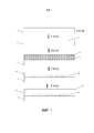
Фигура 1 представляет собой блок-схему, показывающую способ изготовления многослойной подложки по настоящему изобретению.Figure 1 is a block diagram showing a method for manufacturing a multilayer substrate of the present invention.
Фигура 2 представляет собой фотографию растрового электронного микроскопа (РЭМ), показывающую поперечный разрез многослойной подложки согласно изобретению.Figure 2 is a photograph of a scanning electron microscope (SEM) showing a cross section of a multilayer substrate according to the invention.
На Фигуре 1 сначала, на этапе (a) обеспечивают плоскую прозрачную стеклянную подложку 1. Затем, на этапе (b), на одну сторону этой подложки магнетронным напылением наносят слой 2 оксида металла. На следующем этапе (этапе (c)) наносят слой 3 стеклофритты с высоким показателем преломления, например, путем трафаретной печати пасты, включающей в себя стеклофритту и органический носитель (полимер и органический растворитель).In Figure 1, first, in step (a), a flat
Затем, на этапе (d), полученную подложку, несущую на себе слой 2 оксида металла и слой стеклообразующей пасты, подвергают постепенному нагреву, сначала до испарения органического растворителя, затем до выгорания органического полимера, и наконец, до плавления порошка стеклофритты для получения слоя 4 эмали с высоким показателем преломления. В ходе этого конечного этапа нагрева, сферические пустоты 5 образуются на дне слоя стефритты в результате реакции между оксидом металла и стеклофриттой. Сферические пустоты прикрепляются к границе раздела эмали 4 с высоким показателем преломления и не поднимаются к поверхности слоя эмали. Затем, на этапе (e) на гладкую поверхность эмали 4 с высоким показателем преломления наносят прозрачный электропроводящий слой 6.Then, in step (d), the resulting substrate, bearing on itself a
На РЭМ-фотографии на Фигуре 2, темно-серая стеклянная подложка покрыта более светлым серым слоем эмали с высоким показателем преломления. Монослой сферических пустот полностью в него внедрен и находится в контакте с границей раздела между стеклянной подложкой и вышележащей эмалью. Показано, что многослойная подложка еще не содержит прозрачного электропроводящего слоя. Видно, что поверхность слоя эмали с высоким показателем преломления является идеально гладкой и свободна от кратерообразных неровностей поверхности.In the SEM photograph of Figure 2, the dark gray glass substrate is coated with a lighter gray layer of enamel with a high refractive index. A monolayer of spherical voids is fully embedded in it and is in contact with the interface between the glass substrate and the overlying enamel. It is shown that the multilayer substrate does not yet contain a transparent electrically conductive layer. It can be seen that the surface of the enamel layer with a high refractive index is perfectly smooth and free from crater-like surface irregularities.
ПримерExample
Лист кальциево-натриевого стекла толщиной 0,7 мм был покрыт раствором соединения-предшественника TiO2, нанесенным методом центрифугирования. Покрытый лист стекла был затем подвергнут 10-минутному воздействию температуры 150°C, для испарения растворителя, а затем в течение примерно 1 часа - воздействию температуры 400°C, для осуществления уплотнения слоя TiO2.A sheet of calcium-sodium glass with a thickness of 0.7 mm was coated with a solution of the precursor compound TiO 2 , applied by centrifuging. The coated sheet of glass was then subjected to a 10-minute exposure to a temperature of 150 ° C, to evaporate the solvent, and then for about 1 hour to a temperature of 400 ° C, to effect the compaction of the TiO 2 layer.
На полученный стеклянный лист, покрытый TiO2, была методом трафаретной печати нанесена паста, содержащая 75 мас.% стеклофритты с высоким показателем преломления (Bi2O3-B2O3-ZnO-SiO2) и 25 мас.% органического носителя (этилцеллюлозы и органического растворителя), и подвергнута воздействию этапа сушки (10 минут при 150°C).The resulting glass sheet coated with TiO 2 was screen printed with a paste containing 75 wt.% Glass frits with a high refractive index (Bi 2 O 3 -B 2 O 3 -ZnO-SiO 2 ) and 25 wt.% Organic carrier ( ethyl cellulose and an organic solvent), and exposed to a drying step (10 minutes at 150 ° C).
Подложка затем обжигалась в течение примерно 10 минут при 570°C, с получением слоя эмали с высоким показателем преломления (12 мкм), содержащего несколько сферических пустот.The substrate was then calcined for about 10 minutes at 570 ° C to form an enamel layer with a high refractive index (12 μm) containing several spherical voids.
Средний размер сферических пустот и степень нанесения покрытия (площадь поверхности, покрытой TiO2, занимаемой сферическими пустотами) были измерены путем анализа изображений, проведенного на трех различных образцах с возрастающей толщиной слоя TiO2.The average size of the spherical voids and the degree of coating (surface area coated with TiO 2 occupied by spherical voids) were measured by analyzing images on three different samples with increasing thickness of the TiO 2 layer.
Ниже в Таблице показан средний размер сферических пустот, степень нанесения покрытия и степень помутнения полученной подложки, для повышенных содержаний TiO2, по сравнению с отрицательным контролем, сделанным за счет нанесения покрытия в виде стеклофритты с высоким показателем преломления, непосредственно на кальциево-натриевом стекле.The Table below shows the average size of the spherical voids, the degree of coating and the degree of turbidity of the substrate obtained, for elevated TiO 2 contents, compared to the negative control made by applying a coating in the form of glass frits with a high refractive index, directly on calcium-sodium glass.
Слой эмали с высоким показателем преломления согласно отрицательному контролю был свободен от сферических пустот, расположенных на дне слоя эмали.The high refractive index enamel layer, according to the negative control, was free of spherical voids located at the bottom of the enamel layer.
Повышение количества оксида металла привело к повышению среднего размера сферических пустот, образованных на границе раздела стекло/эмаль, области, занимаемой пустотами, и степени помутнения полученного слоя IEL.An increase in the amount of metal oxide led to an increase in the average size of the spherical voids formed at the glass / enamel interface, the area occupied by the voids, and the degree of turbidity of the resulting IEL layer.
Эти экспериментальные данные ясно показывают, что сферические пустоты на дне слоя эмали возникают вследствие взаимодействия слоя оксида металла с вышележащей стеклофриттой с высоким показателем преломления.These experimental data clearly show that spherical voids at the bottom of the enamel layer arise due to the interaction of the metal oxide layer with the overlying glass frit with a high refractive index.
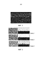
Фигура 3 показывает ракурс проекции (слева) и поперечный разрез (справа) для каждого из вышеприведенных Примеров 1, 2 и 3 согласно настоящему изобретению.Figure 3 shows the perspective view (left) and cross section (right) for each of the above Examples 1, 2 and 3 according to the present invention.
Claims (19)
Applications Claiming Priority (3)
| Application Number | Priority Date | Filing Date | Title |
|---|---|---|---|
| EP14177291.3 | 2014-07-16 | ||
| EP14177291.3A EP2975008B1 (en) | 2014-07-16 | 2014-07-16 | Transparent diffusive oled substrate and method for producing such a substrate |
| PCT/EP2015/064157 WO2016008685A1 (en) | 2014-07-16 | 2015-06-23 | Transparent diffusive oled substrate and method for producing such a substrate |
Publications (3)
| Publication Number | Publication Date |
|---|---|
| RU2017104776A RU2017104776A (en) | 2018-08-16 |
| RU2017104776A3 RU2017104776A3 (en) | 2018-12-25 |
| RU2693123C2 true RU2693123C2 (en) | 2019-07-01 |
Family
ID=51178780
Family Applications (1)
| Application Number | Title | Priority Date | Filing Date |
|---|---|---|---|
| RU2017104776A RU2693123C2 (en) | 2014-07-16 | 2015-06-23 | Oled translucent diffusion substrate and method for making such substrate |
Country Status (10)
| Country | Link |
|---|---|
| US (1) | US10379269B2 (en) |
| EP (1) | EP2975008B1 (en) |
| JP (1) | JP6568197B2 (en) |
| KR (1) | KR20170031142A (en) |
| CN (1) | CN106488893B (en) |
| ES (1) | ES2625733T3 (en) |
| MY (1) | MY181429A (en) |
| RU (1) | RU2693123C2 (en) |
| TW (1) | TWI666804B (en) |
| WO (1) | WO2016008685A1 (en) |
Families Citing this family (4)
| Publication number | Priority date | Publication date | Assignee | Title |
|---|---|---|---|---|
| EP3028999B1 (en) * | 2014-12-01 | 2017-05-24 | Saint-Gobain Glass France | Transparent diffusive oled substrate and method for producing such a substrate |
| US10700242B2 (en) * | 2016-12-27 | 2020-06-30 | Nichia Corporation | Method of producing wavelength conversion member |
| US10650935B2 (en) * | 2017-08-04 | 2020-05-12 | Vitro Flat Glass Llc | Transparent conductive oxide having an embedded film |
| WO2022250995A1 (en) * | 2021-05-25 | 2022-12-01 | OLEDWorks LLC | Segmented oled |
Citations (4)
| Publication number | Priority date | Publication date | Assignee | Title |
|---|---|---|---|---|
| US7691288B2 (en) * | 2005-07-18 | 2010-04-06 | E.I. Du Pont De Nemours And Company | Thick film getter paste compositions with pre-hydrated desiccant for use in atmosphere control |
| US20110001159A1 (en) * | 2008-03-18 | 2011-01-06 | Asahi Glass Company, Limited | Substrate for electronic device, layered body for organic led element, method for manufacturing the same, organic led element, and method for manufacturing the same |
| WO2011046156A1 (en) * | 2009-10-15 | 2011-04-21 | 旭硝子株式会社 | Glass for diffusion layer in organic led element, and organic led element utilizing same |
| US8427045B2 (en) * | 2007-07-27 | 2013-04-23 | Asahi Glass Company, Limited | Translucent substrate, process for producing the same, organic LED element and process for producing the same |
Family Cites Families (8)
| Publication number | Priority date | Publication date | Assignee | Title |
|---|---|---|---|---|
| US20080090034A1 (en) * | 2006-09-18 | 2008-04-17 | Harrison Daniel J | Colored glass frit |
| US8227988B2 (en) * | 2008-09-11 | 2012-07-24 | Samsung Sdi Co., Ltd | Material for forming barrier ribs, barrier ribs formed using the material and PDP comprising the barrier ribs |
| FR2955575B1 (en) * | 2010-01-22 | 2012-02-24 | Saint Gobain | GLASS SUBSTRATE COATED WITH A HIGH INDEX LAYER UNDER AN ELECTRODE COATING AND ORGANIC ELECTROLUMINESCENT DEVICE COMPRISING SUCH A SUBSTRATE. |
| KR20130143547A (en) * | 2010-07-16 | 2013-12-31 | 에이쥐씨 글래스 유럽 | Translucent conductive substrate for organic light emitting devices |
| KR102648076B1 (en) | 2010-11-04 | 2024-03-18 | 지이 비디오 컴프레션, 엘엘씨 | Picture coding supporting block merging and skip mode |
| KR101715112B1 (en) * | 2012-06-14 | 2017-03-10 | 쌩-고벵 글래스 프랑스 | Layered body for OLED, method for manufacturing the same and OLED element having the same |
| KR101493601B1 (en) | 2013-07-17 | 2015-02-13 | 쌩-고벵 글래스 프랑스 | A laminate for a light emitting device and process for preparing thereof |
| CN109074895B (en) * | 2016-08-16 | 2022-05-27 | 浙江凯盈新材料有限公司 | Thick film paste for front side metallization in silicon solar cells |
-
2014
- 2014-07-16 ES ES14177291.3T patent/ES2625733T3/en active Active
- 2014-07-16 EP EP14177291.3A patent/EP2975008B1/en not_active Not-in-force
-
2015
- 2015-06-23 JP JP2017501649A patent/JP6568197B2/en not_active Expired - Fee Related
- 2015-06-23 RU RU2017104776A patent/RU2693123C2/en active
- 2015-06-23 CN CN201580038240.3A patent/CN106488893B/en not_active Expired - Fee Related
- 2015-06-23 MY MYPI2017700108A patent/MY181429A/en unknown
- 2015-06-23 KR KR1020177000858A patent/KR20170031142A/en not_active Application Discontinuation
- 2015-06-23 WO PCT/EP2015/064157 patent/WO2016008685A1/en active Application Filing
- 2015-06-23 US US15/326,311 patent/US10379269B2/en not_active Expired - Fee Related
- 2015-06-29 TW TW104120951A patent/TWI666804B/en not_active IP Right Cessation
Patent Citations (5)
| Publication number | Priority date | Publication date | Assignee | Title |
|---|---|---|---|---|
| US7691288B2 (en) * | 2005-07-18 | 2010-04-06 | E.I. Du Pont De Nemours And Company | Thick film getter paste compositions with pre-hydrated desiccant for use in atmosphere control |
| US8427045B2 (en) * | 2007-07-27 | 2013-04-23 | Asahi Glass Company, Limited | Translucent substrate, process for producing the same, organic LED element and process for producing the same |
| EP2178343B1 (en) * | 2007-07-27 | 2013-05-29 | Asahi Glass Company, Limited | Translucent substrate, method for manufacturing the translucent substrate and organic led element |
| US20110001159A1 (en) * | 2008-03-18 | 2011-01-06 | Asahi Glass Company, Limited | Substrate for electronic device, layered body for organic led element, method for manufacturing the same, organic led element, and method for manufacturing the same |
| WO2011046156A1 (en) * | 2009-10-15 | 2011-04-21 | 旭硝子株式会社 | Glass for diffusion layer in organic led element, and organic led element utilizing same |
Also Published As
| Publication number | Publication date |
|---|---|
| CN106488893A (en) | 2017-03-08 |
| ES2625733T3 (en) | 2017-07-20 |
| RU2017104776A3 (en) | 2018-12-25 |
| JP2017528399A (en) | 2017-09-28 |
| WO2016008685A1 (en) | 2016-01-21 |
| EP2975008A1 (en) | 2016-01-20 |
| TWI666804B (en) | 2019-07-21 |
| KR20170031142A (en) | 2017-03-20 |
| US10379269B2 (en) | 2019-08-13 |
| JP6568197B2 (en) | 2019-08-28 |
| CN106488893B (en) | 2020-08-07 |
| MY181429A (en) | 2020-12-21 |
| RU2017104776A (en) | 2018-08-16 |
| US20170205542A1 (en) | 2017-07-20 |
| EP2975008B1 (en) | 2017-03-01 |
| TW201622204A (en) | 2016-06-16 |
Similar Documents
| Publication | Publication Date | Title |
|---|---|---|
| TWI441790B (en) | A light-transmitting substrate, a method for manufacturing the same, an organic LED device, and a method for manufacturing the same | |
| EP2384086B1 (en) | Substrate for electronic device and electronic device using same | |
| TWI482527B (en) | A light-transmitting substrate, a method for manufacturing the same, an organic LED device, and a method for manufacturing the same | |
| RU2693123C2 (en) | Oled translucent diffusion substrate and method for making such substrate | |
| RU2666962C2 (en) | Laminate for light emitting device and method for its manufacture | |
| TWI555253B (en) | Laminate for light emitting device and process of preparing same | |
| KR20170137087A (en) | Layered structures for OLEDs and methods of making such structures | |
| RU2656264C2 (en) | Transparent diffusive oled substrate and method for producing such substrate | |
| RU2656261C2 (en) | Transparent diffusive oled substrate and method for producing such substrate | |
| JP6608932B2 (en) | Transparent diffusive OLED substrate and method for producing the substrate | |
| JP7538071B2 (en) | Method for manufacturing light-transmitting substrate with light-scattering film, and method for manufacturing organic EL panel |