EP2975008B1 - Transparent diffusive oled substrate and method for producing such a substrate - Google Patents
Transparent diffusive oled substrate and method for producing such a substrate Download PDFInfo
- Publication number
- EP2975008B1 EP2975008B1 EP14177291.3A EP14177291A EP2975008B1 EP 2975008 B1 EP2975008 B1 EP 2975008B1 EP 14177291 A EP14177291 A EP 14177291A EP 2975008 B1 EP2975008 B1 EP 2975008B1
- Authority
- EP
- European Patent Office
- Prior art keywords
- substrate
- layer
- glass
- high index
- metal oxide
- Prior art date
- Legal status (The legal status is an assumption and is not a legal conclusion. Google has not performed a legal analysis and makes no representation as to the accuracy of the status listed.)
- Not-in-force
Links
- 239000000758 substrate Substances 0.000 title claims description 75
- 238000004519 manufacturing process Methods 0.000 title description 3
- 239000010410 layer Substances 0.000 claims description 99
- 239000011521 glass Substances 0.000 claims description 90
- 210000003298 dental enamel Anatomy 0.000 claims description 47
- 229910044991 metal oxide Inorganic materials 0.000 claims description 35
- 150000004706 metal oxides Chemical class 0.000 claims description 35
- GWEVSGVZZGPLCZ-UHFFFAOYSA-N Titan oxide Chemical compound O=[Ti]=O GWEVSGVZZGPLCZ-UHFFFAOYSA-N 0.000 claims description 22
- 238000000034 method Methods 0.000 claims description 16
- 238000010304 firing Methods 0.000 claims description 10
- WMWLMWRWZQELOS-UHFFFAOYSA-N bismuth(iii) oxide Chemical compound O=[Bi]O[Bi]=O WMWLMWRWZQELOS-UHFFFAOYSA-N 0.000 claims description 8
- MCMNRKCIXSYSNV-UHFFFAOYSA-N Zirconium dioxide Chemical compound O=[Zr]=O MCMNRKCIXSYSNV-UHFFFAOYSA-N 0.000 claims description 6
- 239000011248 coating agent Substances 0.000 claims description 6
- 238000000576 coating method Methods 0.000 claims description 6
- ZKATWMILCYLAPD-UHFFFAOYSA-N niobium pentoxide Chemical compound O=[Nb](=O)O[Nb](=O)=O ZKATWMILCYLAPD-UHFFFAOYSA-N 0.000 claims description 6
- XOLBLPGZBRYERU-UHFFFAOYSA-N tin dioxide Chemical compound O=[Sn]=O XOLBLPGZBRYERU-UHFFFAOYSA-N 0.000 claims description 6
- 230000008018 melting Effects 0.000 claims description 5
- 238000002844 melting Methods 0.000 claims description 5
- 239000000203 mixture Substances 0.000 claims description 5
- PNEYBMLMFCGWSK-UHFFFAOYSA-N aluminium oxide Inorganic materials [O-2].[O-2].[O-2].[Al+3].[Al+3] PNEYBMLMFCGWSK-UHFFFAOYSA-N 0.000 claims description 4
- 229910052593 corundum Inorganic materials 0.000 claims description 4
- 229910001845 yogo sapphire Inorganic materials 0.000 claims description 4
- QZQVBEXLDFYHSR-UHFFFAOYSA-N gallium(III) oxide Inorganic materials O=[Ga]O[Ga]=O QZQVBEXLDFYHSR-UHFFFAOYSA-N 0.000 claims description 3
- CJNBYAVZURUTKZ-UHFFFAOYSA-N hafnium(IV) oxide Inorganic materials O=[Hf]=O CJNBYAVZURUTKZ-UHFFFAOYSA-N 0.000 claims description 3
- PJXISJQVUVHSOJ-UHFFFAOYSA-N indium(III) oxide Inorganic materials [O-2].[O-2].[O-2].[In+3].[In+3] PJXISJQVUVHSOJ-UHFFFAOYSA-N 0.000 claims description 3
- 239000002356 single layer Substances 0.000 claims description 3
- PBCFLUZVCVVTBY-UHFFFAOYSA-N tantalum pentoxide Inorganic materials O=[Ta](=O)O[Ta](=O)=O PBCFLUZVCVVTBY-UHFFFAOYSA-N 0.000 claims description 3
- ZNOKGRXACCSDPY-UHFFFAOYSA-N tungsten(VI) oxide Inorganic materials O=[W](=O)=O ZNOKGRXACCSDPY-UHFFFAOYSA-N 0.000 claims description 3
- 238000000605 extraction Methods 0.000 description 11
- 239000012044 organic layer Substances 0.000 description 8
- 239000002245 particle Substances 0.000 description 8
- 238000000149 argon plasma sintering Methods 0.000 description 6
- 238000006243 chemical reaction Methods 0.000 description 6
- 239000011159 matrix material Substances 0.000 description 6
- 230000015572 biosynthetic process Effects 0.000 description 4
- 239000003960 organic solvent Substances 0.000 description 4
- 239000007787 solid Substances 0.000 description 4
- 239000001856 Ethyl cellulose Substances 0.000 description 3
- ZZSNKZQZMQGXPY-UHFFFAOYSA-N Ethyl cellulose Chemical compound CCOCC1OC(OC)C(OCC)C(OCC)C1OC1C(O)C(O)C(OC)C(CO)O1 ZZSNKZQZMQGXPY-UHFFFAOYSA-N 0.000 description 3
- 239000000975 dye Substances 0.000 description 3
- 229920001249 ethyl cellulose Polymers 0.000 description 3
- 235000019325 ethyl cellulose Nutrition 0.000 description 3
- 238000010438 heat treatment Methods 0.000 description 3
- 238000001755 magnetron sputter deposition Methods 0.000 description 3
- 239000013642 negative control Substances 0.000 description 3
- 230000000630 rising effect Effects 0.000 description 3
- 239000005361 soda-lime glass Substances 0.000 description 3
- XLYOFNOQVPJJNP-UHFFFAOYSA-N water Substances O XLYOFNOQVPJJNP-UHFFFAOYSA-N 0.000 description 3
- VYPSYNLAJGMNEJ-UHFFFAOYSA-N Silicium dioxide Chemical compound O=[Si]=O VYPSYNLAJGMNEJ-UHFFFAOYSA-N 0.000 description 2
- -1 TiO2 Chemical class 0.000 description 2
- 238000000231 atomic layer deposition Methods 0.000 description 2
- 238000000280 densification Methods 0.000 description 2
- 239000012530 fluid Substances 0.000 description 2
- 238000007650 screen-printing Methods 0.000 description 2
- 239000002904 solvent Substances 0.000 description 2
- 239000011800 void material Substances 0.000 description 2
- KKCBUQHMOMHUOY-UHFFFAOYSA-N Na2O Inorganic materials [O-2].[Na+].[Na+] KKCBUQHMOMHUOY-UHFFFAOYSA-N 0.000 description 1
- 229910007676 ZnO—SiO2 Inorganic materials 0.000 description 1
- 238000004458 analytical method Methods 0.000 description 1
- 230000004888 barrier function Effects 0.000 description 1
- 239000011230 binding agent Substances 0.000 description 1
- 230000005540 biological transmission Effects 0.000 description 1
- CETPSERCERDGAM-UHFFFAOYSA-N ceric oxide Chemical compound O=[Ce]=O CETPSERCERDGAM-UHFFFAOYSA-N 0.000 description 1
- 229910000422 cerium(IV) oxide Inorganic materials 0.000 description 1
- 239000007795 chemical reaction product Substances 0.000 description 1
- 229910052681 coesite Inorganic materials 0.000 description 1
- 238000007796 conventional method Methods 0.000 description 1
- 238000010168 coupling process Methods 0.000 description 1
- 238000005859 coupling reaction Methods 0.000 description 1
- 229910052906 cristobalite Inorganic materials 0.000 description 1
- 239000013078 crystal Substances 0.000 description 1
- 229910021488 crystalline silicon dioxide Inorganic materials 0.000 description 1
- 230000006378 damage Effects 0.000 description 1
- 230000007547 defect Effects 0.000 description 1
- 238000001035 drying Methods 0.000 description 1
- 230000000694 effects Effects 0.000 description 1
- 239000002320 enamel (paints) Substances 0.000 description 1
- 238000005530 etching Methods 0.000 description 1
- 239000005357 flat glass Substances 0.000 description 1
- 230000004927 fusion Effects 0.000 description 1
- 238000010191 image analysis Methods 0.000 description 1
- AMGQUBHHOARCQH-UHFFFAOYSA-N indium;oxotin Chemical compound [In].[Sn]=O AMGQUBHHOARCQH-UHFFFAOYSA-N 0.000 description 1
- 229910052500 inorganic mineral Inorganic materials 0.000 description 1
- 230000003993 interaction Effects 0.000 description 1
- 238000010030 laminating Methods 0.000 description 1
- 239000007788 liquid Substances 0.000 description 1
- 239000011707 mineral Substances 0.000 description 1
- 239000006060 molten glass Substances 0.000 description 1
- 230000005693 optoelectronics Effects 0.000 description 1
- 229920000620 organic polymer Polymers 0.000 description 1
- 238000005325 percolation Methods 0.000 description 1
- 229920000642 polymer Polymers 0.000 description 1
- 239000000843 powder Substances 0.000 description 1
- 239000002243 precursor Substances 0.000 description 1
- 239000000047 product Substances 0.000 description 1
- 239000000377 silicon dioxide Substances 0.000 description 1
- 238000007764 slot die coating Methods 0.000 description 1
- 238000007711 solidification Methods 0.000 description 1
- 238000000935 solvent evaporation Methods 0.000 description 1
- 229910052682 stishovite Inorganic materials 0.000 description 1
- 239000002344 surface layer Substances 0.000 description 1
- 230000003746 surface roughness Effects 0.000 description 1
- 229910052905 tridymite Inorganic materials 0.000 description 1
Images

Classifications
-
- G—PHYSICS
- G02—OPTICS
- G02B—OPTICAL ELEMENTS, SYSTEMS OR APPARATUS
- G02B5/00—Optical elements other than lenses
- G02B5/02—Diffusing elements; Afocal elements
- G02B5/0268—Diffusing elements; Afocal elements characterized by the fabrication or manufacturing method
-
- C—CHEMISTRY; METALLURGY
- C03—GLASS; MINERAL OR SLAG WOOL
- C03C—CHEMICAL COMPOSITION OF GLASSES, GLAZES OR VITREOUS ENAMELS; SURFACE TREATMENT OF GLASS; SURFACE TREATMENT OF FIBRES OR FILAMENTS MADE FROM GLASS, MINERALS OR SLAGS; JOINING GLASS TO GLASS OR OTHER MATERIALS
- C03C17/00—Surface treatment of glass, not in the form of fibres or filaments, by coating
- C03C17/006—Surface treatment of glass, not in the form of fibres or filaments, by coating with materials of composite character
- C03C17/007—Surface treatment of glass, not in the form of fibres or filaments, by coating with materials of composite character containing a dispersed phase, e.g. particles, fibres or flakes, in a continuous phase
-
- C—CHEMISTRY; METALLURGY
- C03—GLASS; MINERAL OR SLAG WOOL
- C03C—CHEMICAL COMPOSITION OF GLASSES, GLAZES OR VITREOUS ENAMELS; SURFACE TREATMENT OF GLASS; SURFACE TREATMENT OF FIBRES OR FILAMENTS MADE FROM GLASS, MINERALS OR SLAGS; JOINING GLASS TO GLASS OR OTHER MATERIALS
- C03C17/00—Surface treatment of glass, not in the form of fibres or filaments, by coating
- C03C17/02—Surface treatment of glass, not in the form of fibres or filaments, by coating with glass
- C03C17/04—Surface treatment of glass, not in the form of fibres or filaments, by coating with glass by fritting glass powder
-
- C—CHEMISTRY; METALLURGY
- C03—GLASS; MINERAL OR SLAG WOOL
- C03C—CHEMICAL COMPOSITION OF GLASSES, GLAZES OR VITREOUS ENAMELS; SURFACE TREATMENT OF GLASS; SURFACE TREATMENT OF FIBRES OR FILAMENTS MADE FROM GLASS, MINERALS OR SLAGS; JOINING GLASS TO GLASS OR OTHER MATERIALS
- C03C17/00—Surface treatment of glass, not in the form of fibres or filaments, by coating
- C03C17/22—Surface treatment of glass, not in the form of fibres or filaments, by coating with other inorganic material
- C03C17/23—Oxides
-
- C—CHEMISTRY; METALLURGY
- C03—GLASS; MINERAL OR SLAG WOOL
- C03C—CHEMICAL COMPOSITION OF GLASSES, GLAZES OR VITREOUS ENAMELS; SURFACE TREATMENT OF GLASS; SURFACE TREATMENT OF FIBRES OR FILAMENTS MADE FROM GLASS, MINERALS OR SLAGS; JOINING GLASS TO GLASS OR OTHER MATERIALS
- C03C17/00—Surface treatment of glass, not in the form of fibres or filaments, by coating
- C03C17/34—Surface treatment of glass, not in the form of fibres or filaments, by coating with at least two coatings having different compositions
- C03C17/3411—Surface treatment of glass, not in the form of fibres or filaments, by coating with at least two coatings having different compositions with at least two coatings of inorganic materials
- C03C17/3417—Surface treatment of glass, not in the form of fibres or filaments, by coating with at least two coatings having different compositions with at least two coatings of inorganic materials all coatings being oxide coatings
-
- C—CHEMISTRY; METALLURGY
- C03—GLASS; MINERAL OR SLAG WOOL
- C03C—CHEMICAL COMPOSITION OF GLASSES, GLAZES OR VITREOUS ENAMELS; SURFACE TREATMENT OF GLASS; SURFACE TREATMENT OF FIBRES OR FILAMENTS MADE FROM GLASS, MINERALS OR SLAGS; JOINING GLASS TO GLASS OR OTHER MATERIALS
- C03C17/00—Surface treatment of glass, not in the form of fibres or filaments, by coating
- C03C17/34—Surface treatment of glass, not in the form of fibres or filaments, by coating with at least two coatings having different compositions
- C03C17/36—Surface treatment of glass, not in the form of fibres or filaments, by coating with at least two coatings having different compositions at least one coating being a metal
- C03C17/3602—Surface treatment of glass, not in the form of fibres or filaments, by coating with at least two coatings having different compositions at least one coating being a metal the metal being present as a layer
- C03C17/3657—Surface treatment of glass, not in the form of fibres or filaments, by coating with at least two coatings having different compositions at least one coating being a metal the metal being present as a layer the multilayer coating having optical properties
-
- C—CHEMISTRY; METALLURGY
- C03—GLASS; MINERAL OR SLAG WOOL
- C03C—CHEMICAL COMPOSITION OF GLASSES, GLAZES OR VITREOUS ENAMELS; SURFACE TREATMENT OF GLASS; SURFACE TREATMENT OF FIBRES OR FILAMENTS MADE FROM GLASS, MINERALS OR SLAGS; JOINING GLASS TO GLASS OR OTHER MATERIALS
- C03C8/00—Enamels; Glazes; Fusion seal compositions being frit compositions having non-frit additions
- C03C8/02—Frit compositions, i.e. in a powdered or comminuted form
-
- G—PHYSICS
- G02—OPTICS
- G02B—OPTICAL ELEMENTS, SYSTEMS OR APPARATUS
- G02B5/00—Optical elements other than lenses
- G02B5/02—Diffusing elements; Afocal elements
- G02B5/0205—Diffusing elements; Afocal elements characterised by the diffusing properties
- G02B5/0236—Diffusing elements; Afocal elements characterised by the diffusing properties the diffusion taking place within the volume of the element
- G02B5/0247—Diffusing elements; Afocal elements characterised by the diffusing properties the diffusion taking place within the volume of the element by means of voids or pores
-
- G—PHYSICS
- G02—OPTICS
- G02B—OPTICAL ELEMENTS, SYSTEMS OR APPARATUS
- G02B5/00—Optical elements other than lenses
- G02B5/02—Diffusing elements; Afocal elements
- G02B5/0273—Diffusing elements; Afocal elements characterized by the use
- G02B5/0278—Diffusing elements; Afocal elements characterized by the use used in transmission
-
- H—ELECTRICITY
- H05—ELECTRIC TECHNIQUES NOT OTHERWISE PROVIDED FOR
- H05B—ELECTRIC HEATING; ELECTRIC LIGHT SOURCES NOT OTHERWISE PROVIDED FOR; CIRCUIT ARRANGEMENTS FOR ELECTRIC LIGHT SOURCES, IN GENERAL
- H05B33/00—Electroluminescent light sources
- H05B33/02—Details
-
- H—ELECTRICITY
- H05—ELECTRIC TECHNIQUES NOT OTHERWISE PROVIDED FOR
- H05B—ELECTRIC HEATING; ELECTRIC LIGHT SOURCES NOT OTHERWISE PROVIDED FOR; CIRCUIT ARRANGEMENTS FOR ELECTRIC LIGHT SOURCES, IN GENERAL
- H05B33/00—Electroluminescent light sources
- H05B33/10—Apparatus or processes specially adapted to the manufacture of electroluminescent light sources
-
- H—ELECTRICITY
- H05—ELECTRIC TECHNIQUES NOT OTHERWISE PROVIDED FOR
- H05B—ELECTRIC HEATING; ELECTRIC LIGHT SOURCES NOT OTHERWISE PROVIDED FOR; CIRCUIT ARRANGEMENTS FOR ELECTRIC LIGHT SOURCES, IN GENERAL
- H05B33/00—Electroluminescent light sources
- H05B33/12—Light sources with substantially two-dimensional radiating surfaces
- H05B33/22—Light sources with substantially two-dimensional radiating surfaces characterised by the chemical or physical composition or the arrangement of auxiliary dielectric or reflective layers
-
- H—ELECTRICITY
- H10—SEMICONDUCTOR DEVICES; ELECTRIC SOLID-STATE DEVICES NOT OTHERWISE PROVIDED FOR
- H10K—ORGANIC ELECTRIC SOLID-STATE DEVICES
- H10K50/00—Organic light-emitting devices
- H10K50/80—Constructional details
- H10K50/85—Arrangements for extracting light from the devices
- H10K50/854—Arrangements for extracting light from the devices comprising scattering means
-
- H—ELECTRICITY
- H10—SEMICONDUCTOR DEVICES; ELECTRIC SOLID-STATE DEVICES NOT OTHERWISE PROVIDED FOR
- H10K—ORGANIC ELECTRIC SOLID-STATE DEVICES
- H10K77/00—Constructional details of devices covered by this subclass and not covered by groups H10K10/80, H10K30/80, H10K50/80 or H10K59/80
- H10K77/10—Substrates, e.g. flexible substrates
-
- C—CHEMISTRY; METALLURGY
- C03—GLASS; MINERAL OR SLAG WOOL
- C03C—CHEMICAL COMPOSITION OF GLASSES, GLAZES OR VITREOUS ENAMELS; SURFACE TREATMENT OF GLASS; SURFACE TREATMENT OF FIBRES OR FILAMENTS MADE FROM GLASS, MINERALS OR SLAGS; JOINING GLASS TO GLASS OR OTHER MATERIALS
- C03C2217/00—Coatings on glass
- C03C2217/40—Coatings comprising at least one inhomogeneous layer
- C03C2217/43—Coatings comprising at least one inhomogeneous layer consisting of a dispersed phase in a continuous phase
- C03C2217/44—Coatings comprising at least one inhomogeneous layer consisting of a dispersed phase in a continuous phase characterized by the composition of the continuous phase
- C03C2217/45—Inorganic continuous phases
- C03C2217/452—Glass
-
- C—CHEMISTRY; METALLURGY
- C03—GLASS; MINERAL OR SLAG WOOL
- C03C—CHEMICAL COMPOSITION OF GLASSES, GLAZES OR VITREOUS ENAMELS; SURFACE TREATMENT OF GLASS; SURFACE TREATMENT OF FIBRES OR FILAMENTS MADE FROM GLASS, MINERALS OR SLAGS; JOINING GLASS TO GLASS OR OTHER MATERIALS
- C03C2217/00—Coatings on glass
- C03C2217/40—Coatings comprising at least one inhomogeneous layer
- C03C2217/43—Coatings comprising at least one inhomogeneous layer consisting of a dispersed phase in a continuous phase
- C03C2217/46—Coatings comprising at least one inhomogeneous layer consisting of a dispersed phase in a continuous phase characterized by the dispersed phase
- C03C2217/48—Coatings comprising at least one inhomogeneous layer consisting of a dispersed phase in a continuous phase characterized by the dispersed phase having a specific function
-
- C—CHEMISTRY; METALLURGY
- C03—GLASS; MINERAL OR SLAG WOOL
- C03C—CHEMICAL COMPOSITION OF GLASSES, GLAZES OR VITREOUS ENAMELS; SURFACE TREATMENT OF GLASS; SURFACE TREATMENT OF FIBRES OR FILAMENTS MADE FROM GLASS, MINERALS OR SLAGS; JOINING GLASS TO GLASS OR OTHER MATERIALS
- C03C2217/00—Coatings on glass
- C03C2217/70—Properties of coatings
- C03C2217/73—Anti-reflective coatings with specific characteristics
- C03C2217/734—Anti-reflective coatings with specific characteristics comprising an alternation of high and low refractive indexes
-
- C—CHEMISTRY; METALLURGY
- C03—GLASS; MINERAL OR SLAG WOOL
- C03C—CHEMICAL COMPOSITION OF GLASSES, GLAZES OR VITREOUS ENAMELS; SURFACE TREATMENT OF GLASS; SURFACE TREATMENT OF FIBRES OR FILAMENTS MADE FROM GLASS, MINERALS OR SLAGS; JOINING GLASS TO GLASS OR OTHER MATERIALS
- C03C2217/00—Coatings on glass
- C03C2217/90—Other aspects of coatings
- C03C2217/91—Coatings containing at least one layer having a composition gradient through its thickness
-
- C—CHEMISTRY; METALLURGY
- C03—GLASS; MINERAL OR SLAG WOOL
- C03C—CHEMICAL COMPOSITION OF GLASSES, GLAZES OR VITREOUS ENAMELS; SURFACE TREATMENT OF GLASS; SURFACE TREATMENT OF FIBRES OR FILAMENTS MADE FROM GLASS, MINERALS OR SLAGS; JOINING GLASS TO GLASS OR OTHER MATERIALS
- C03C2217/00—Coatings on glass
- C03C2217/90—Other aspects of coatings
- C03C2217/94—Transparent conductive oxide layers [TCO] being part of a multilayer coating
- C03C2217/948—Layers comprising indium tin oxide [ITO]
-
- H—ELECTRICITY
- H10—SEMICONDUCTOR DEVICES; ELECTRIC SOLID-STATE DEVICES NOT OTHERWISE PROVIDED FOR
- H10K—ORGANIC ELECTRIC SOLID-STATE DEVICES
- H10K2102/00—Constructional details relating to the organic devices covered by this subclass
-
- Y—GENERAL TAGGING OF NEW TECHNOLOGICAL DEVELOPMENTS; GENERAL TAGGING OF CROSS-SECTIONAL TECHNOLOGIES SPANNING OVER SEVERAL SECTIONS OF THE IPC; TECHNICAL SUBJECTS COVERED BY FORMER USPC CROSS-REFERENCE ART COLLECTIONS [XRACs] AND DIGESTS
- Y02—TECHNOLOGIES OR APPLICATIONS FOR MITIGATION OR ADAPTATION AGAINST CLIMATE CHANGE
- Y02E—REDUCTION OF GREENHOUSE GAS [GHG] EMISSIONS, RELATED TO ENERGY GENERATION, TRANSMISSION OR DISTRIBUTION
- Y02E10/00—Energy generation through renewable energy sources
- Y02E10/50—Photovoltaic [PV] energy
- Y02E10/549—Organic PV cells
Definitions
- the present invention is drawn to a new method for producing translucent, light-scattering glass substrates for organic light emitting diodes (OLEDs) and to substrates obtainable by such a method.
- OLEDs are opto-electronic elements comprising a stack of organic layers with fluorescent or phosphorescent dyes sandwiched between two electrodes, at least one of which is translucent. When a voltage is applied to the electrodes the electrons injected from the cathode and the holes injected from the anode combine within the organic layers, resulting in light emission from the fluorescent/phosphorescent layers.
- Such light scattering layers have a transparent matrix with a high refractive index close to the TCL refractive index and contain a plurality of light scattering elements having a refractive index different from that of the matrix.
- Such high index matrices are commonly obtained by fusing a high index glass frit thereby obtaining thin high index enamel layers on low index glass substrates.
- the light scattering elements may be solid particles added to the glass frit before the fusing step, crystals formed during the fusing step or air bubbles formed during the fusing step.
- IEL internal extraction layers
- EEL External extraction layers
- the present invention is in the field of internal extraction layers (IEL) having a transparent high index glass matrix containing air bubbles as low index diffusing elements.
- IEL internal extraction layers
- Such IEL with light diffusing air bubbles are advantageous over similar IEL with solid particles because there is no risk of large sized particles protruding from the matrix and generating short-circuits and/or inter-electrode leakage currents in the final OLED product.
- EP 2 178 343 B1 discloses a translucent glass substrate for OLEDs with an internal extraction layer (scattering layer) comprising a high index glass matrix and air bubble scattering elements.
- the surface of the scattering layer is free of surface defects due to open air bubble craters (see [0026] to [0028], and Fig 55).
- a thorough analysis of this document and in particular of [0202] shows however that this result is simply an artifact due to an inappropriate method of counting the scattering elements in the lower surface layers.
- Such a scattering layer has a very high surface quality with an open bubble density of less than 0.1/cm 2 , but suffers from the inconvenience that water or other fluids coming into contact with the edges of the laminate substrate may percolate through the interconnected voids over large areas of the laminate and, through pinholes, into the stack of organic layers with fluorescent or phosphorescent dyes, resulting in destruction of said layers.
- the Applicant surprisingly found that a high number of individual air bubbles formed in the lower layer of a melting high index frit, sticking to the underlying glass substrate essentially without rising to the surface, when the glass frit was applied and fused not directly in contact with the glass substrate but on a thin metal oxide layer coated onto said glass surface beforehand.
- the subject-matter of the present application is a method for preparing a laminate substrate for a light emitting as defined in claim 1.
- Another subject-matter of the present application is a laminate substrate obtainable by the above method as defined in claim 7.
- the glass substrate provided in step (a) is a flat translucent or transparent substrate of mineral glass, for example soda lime glass, generally having a thickness of between 0.1 and 5 mm, preferably of between 0.3 and 1.6 mm.
- Its light transmission ISO9050 standard, illuminant D65 (TLD) such as defined by ISO/IEC 10526 standard in considering the standard colorimetric observer CIE 1931 as defined by the ISO / IEC 10527
- TLD illuminant D65
- a thin layer of a metal oxide is coated by any suitable method onto one side of the flat glass substrate, preferably by reactive or non-reactive magnetron sputtering, atomic layer deposition (ALD) or sol-gel wet coating.
- Said metal oxide layer may cover the whole surface of one side of the glass substrate.
- only part of the surface of the substrate is coated with the metal oxide layer. It could be particularly interesting to coat the substrate with a patterned metal oxide layer in order to prepare a final laminate substrate with a non-uniform extraction pattern.
- the Applicant thinks that the light scattering spherical voids are generated during the firing step (d) by reaction between the metal oxide and a component of the overlying high index glass frit.
- the specific nature of said reaction has not yet been fully elucidated. It is thought that O 2 gas could evolve as a reaction product.
- the majority of the spherical voids are not just air bubbles entrapped in the glass frit during the fusion-solidification steps, such as described in EP 2 178 343 B1 , but gas bubbles generated during the firing step.
- the Applicant observed that the density of spherical voids is far higher in areas where the glass frit layer is coated onto the metal oxide layer than in areas where it is coated directly onto the bare glass substrate.
- the thickness of the metal oxide layer there is no specific limit to the thickness of the metal oxide layer as long as it provides enough reactive components for generating a significant amount of spherical voids in the lower half of the resulting enamel layer.
- a metal oxide layer of a few nanometers only has turned out to be able to trigger the formation of the desirable spherical voids.
- the metal oxide layer preferably has a thickness of between 5 and 80 nm, more preferably of between 10 and 40 nm, and even more preferably of between 15 and 30 nm.
- the Applicant had experimentally shown that at least three metal oxides, i.e. TiO 2 , Al 2 O 3 , ZrO 2 , led to formation of spherical voids near the glass frit interface.
- the skilled person without departing from the present invention, may easily replace these metal oxides by different metal oxides such as, Nb 2 O 5 , HfO 2 , Ta 2 O 5 , WO 3 , Ga 2 O 3 , In 2 O 3 and SnO 2 , or mixtures thereof in order to complete the experimental work of the Applicant and find additional metal oxides suitable for use in the method of the present invention.
- the metal oxide consequently is selected from the group consisting of TiO 2 , Al 2 O 3 , ZrO 2 , Nb 2 O 5 , HfO 2 , Ta 2 O 5 , WO 3 , Ga 2 O 3 , In 2 O 3 , SnO 2 , and mixtures thereof.
- the side of the glass substrate carrying the patterned or non-patterned thin metal oxide layer is then coated with a high index glass frit.
- the refractive index of said glass frit is preferably comprised between 1.70 and 2.20, more preferably between 1.80 and 2.10.
- the high index glass frit advantageously comprises at least 50 weight % and more preferably at least 60 weight % of Bi 2 O 3 .
- the glass frit should be selected to have a melting point (Littleton point) comprised between 450 °C and 570 °C and should lead to an enamel having a refractive index of 1.8 to 2.1.
- Preferred glass frits have the following composition:
- the glass frit particles (70 - 80 wt%) are mixed with 20 - 30 wt% of an organic vehicle (ethyl cellulose and organic solvent).
- the resulting frit paste is then applied onto the metal oxide-coated glass substrate by screen printing or slot die coating.
- the resulting layer is dried by heating at a temperature of 120 - 200 °C.
- the organic binder ethyl cellulose
- the firing step i.e. the fusing of the high index glass frit, resulting in the final enamel is carried out at a temperature of preferably between 540 °C and 600 °C.
- the resulting enamels have been shown to have a surface roughness with an arithmetical mean deviation R a (ISO 4287) of less than 3 nm when measured by AFM on an area of 10 ⁇ m x 10 ⁇ m.
- the amount of the high index glass frit coated onto the metal oxide layer is generally comprised between 20 and 200 g/m 2 , preferably between 25 and 150 g/m 2 , more preferably between 30 and 100 g/m 2 , and most preferably between 35 and 70 g/m 2 .
- the glass frit is heated to a temperature above the Littleton temperature of the glass frit, resulting in fusion of the glass frit, reaction of components of the glass frit with components of the underlying metal oxide, and formation of spherical voids in this reaction zone.
- the metal oxide layer is digested by the glass frit creating locally a glass frit with a slightly different composition. It is therefore impossible to specify the thickness of each of these two layers.
- the overall thickness of the solidified enamel layer hereafter called “high index enamel layer” comprising a plurality of spherical voids (scattering elements) embedded therein is preferably comprised between 3 ⁇ m and 25 ⁇ m, more preferably between 4 ⁇ m and 20 ⁇ m and most preferably between 5 ⁇ m and 15 ⁇ m.
- step (d) To efficiently hold the spherical voids near the bottom of the high index enamel layer and prevent them from rising to the surface, the firing temperature of step (d) however should not be excessively high and the duration of the firing step should not be excessively long.
- the duration of the firing step (d) is preferably comprised between 3 and 30 minutes, more preferably between 5 and 20 minutes.
- the high index glass frit used in the present invention and the enamel resulting therefrom should preferably be substantially devoid of solid scattering particles such as crystalline SiO 2 or TiO 2 particles. Such particles are commonly used as scattering elements in internal extraction layers but require an additional planarization layer, thereby undesirably increasing the total thickness of extraction layer.
- the spherical voids formed during the firing step are not randomly distributed throughout the thickness of the high index enamel layer but are located predominantly in the "lower" half, i.e. near the interface of said enamel layer with the underlying glass substrate.
- the spherical voids of course must be significantly smaller than the thickness of the enamel layer.
- At least 95 %, preferably at least 99 %, and more preferably essentially all of the spherical air voids have a diameter smaller than the half-thickness of the enamel layer and are located in the lower half of the high index enamel layer near the interface with the underlying glass substrate.
- the expression "located in the lower half of the high index enamel layer” means that at least 80 % of the void's volume is located below the median plane of the enamel layer.
- the spherical voids preferably have an average equivalent spherical diameter of between 0.2 ⁇ m and 8 ⁇ m, more preferably of between 0.4 ⁇ m and 4 ⁇ m, and most preferably of between 0.5 ⁇ m and 3 ⁇ m.
- the spherical voids are randomly distributed over the whole area corresponding to the surface of the glass substrate previously coated with the metal oxide layer.
- the density of the spherical voids preferably is comprised between 10 4 and 25.10 6 per mm 2 , more preferably between 10 5 and 5.10 6 per mm 2 .
- the spherical voids When viewed from a direction perpendicular to the general plane of the substrate (projection view), the spherical voids preferably occupy at least 20 %, more preferably at least 25 % of the surface and at most 80 % more preferably at most 70 % of the surface of the substrate previously covered by the metal oxide.
- the laminate substrate of the present invention is meant to be used as a translucent substrate for the production of bottom emitting OLEDs.
- a bottom emitting OLED comprises a translucent substrate carrying a translucent electrode, generally the anode, and a light reflecting electrode, generally the cathode. Light emitted from the stack of light-emitting organic layers is either emitted directly via the translucent anode and substrate or first reflected by the cathode towards and through the translucent anode and substrate.
- the laminate substrate of the present invention consequently further comprises a transparent electro-conductive layer on the high index enamel layer, this electro-conductive layer preferably being directly in contact with the enamel layer or being coated onto an intermediate layer, for example a barrier layer or protection layer.
- the method of the present invention therefore further comprises an additional step of coating a transparent electro-conductive layer (TCL) on the high index enamel layer.
- This layer preferably is a transparent conductive oxide such as ITO (indium tin oxide). Formation of such a TCL may be carried out according to conventional methods familiar to the skilled person, such as magnetron sputtering.
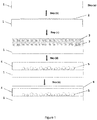
- Figure 1 is a flowchart showing the process of preparing the laminate substrate of the present invention
- Figure 2 is a Scanning Electronic Microscope (SEM) photograph showing a cross-sectional view of a laminate substrate according to the invention
- a flat transparent glass substrate 1 is first provided in step (a).
- a metal oxide layer 2 is then coated onto one side of this substrate by magnetron sputtering.
- a layer 3 of a high index glass frit is applied for example by screen printing a paste including the glass frit and an organic medium (polymer & organic solvent).
- the resulting substrate carrying the metal oxide layer 2 and glass paste layer 3 is then submitted in step (d) to a stepwise heating to first evaporate the organic solvent, then burn out the organic polymer and eventually fuse the glass frit powder to obtain a high index enamel layer 4.
- spherical voids 5 form at the bottom of the glass frit layer from reaction between the metal oxide and the glass frit.
- the spherical voids stick to the interface of the high index enamel 4 and do not rise to the surface of the enamel layer.
- a transparent electro-conducting layer 6 is then coated, in step (e), onto the smooth surface of the high index enamel 4.
- the dark grey glass substrate is covered by a lighter grey layer of high index enamel.
- a monolayer of spherical voids is completely embedded therein and located in contact with the interface between the glass substrate and the overlying enamel.
- the laminate substrate shown does not yet comprise a transparent electro-conducting layer.
- One can see that the surface of the high index enamel layer is perfectly smooth and free of crater-like surface irregularities.
- a 0.7 mm soda lime glass sheet was spin coated with a solution of a TiO 2 precursor.
- the coated glass sheet was then submitted for 10 minutes to a temperature of 150 °C for solvent evaporation and then for about 1 hour to a temperature of 400 °C to effect densification of the TiO 2 layer.
- the resulting TiO 2 -coated glass sheet was screen printed with a paste comprising 75 wt % of a high index glass frit (Bi 2 O 3 -B 2 O 3 -ZnO-SiO 2 ) and 25 wt % of an organic medium (ethyl cellulose and organic solvent) and submitted to a drying step (10 minutes at 150 °C).
- a paste comprising 75 wt % of a high index glass frit (Bi 2 O 3 -B 2 O 3 -ZnO-SiO 2 ) and 25 wt % of an organic medium (ethyl cellulose and organic solvent) and submitted to a drying step (10 minutes at 150 °C).
- the substrate was then fired for about 10 minutes at 570 °C resulting in a high index enamel layer (12 ⁇ m) containing a plurality of spherical voids.
- the mean size of the spherical voids and the coverage rate (area of the TiO 2 -coated surface occupied by the spherical voids) were measured by image analysis on three different samples with increasing TiO 2 layer thickness.
- the below table shows the mean size of the spherical voids, the coverage rate, and the haze ratio of the resulting substrate for increasing amounts of TiO 2 in comparison with a negative control made by coating of the high index glass frit directly on the soda lime glass.
- Negative control Example 1 Example 2
- Example 3 Thickness of the TiO 2 layer after densification 0 26 nm 32 nm 39 nm
- the high index enamel layer of the negative control was free of spherical voids located at the bottom of the enamel layer.
- Figure 3 shows a projection view (left) and a cross-sectional view (right) for each of the above examples 1, 2 and 3 according to the present invention.
Description
- The present invention is drawn to a new method for producing translucent, light-scattering glass substrates for organic light emitting diodes (OLEDs) and to substrates obtainable by such a method.
- OLEDs are opto-electronic elements comprising a stack of organic layers with fluorescent or phosphorescent dyes sandwiched between two electrodes, at least one of which is translucent. When a voltage is applied to the electrodes the electrons injected from the cathode and the holes injected from the anode combine within the organic layers, resulting in light emission from the fluorescent/phosphorescent layers.
- It is commonly known that light extraction from conventional OLEDs is rather poor, most of the light being trapped by total internal reflection in the high index organic layers and transparent conductive layers (TCL). Total internal reflection takes place not only at the boundary between the high index TCL and the underlying glass substrate (refractive index of about 1.5) but also at the boundary between the glass and the air.
- According to estimates, in conventional OLEDs not comprising any additional extraction layer about 60 % of the light emitted from the organic layers is trapped at the TCL/glass boundary, an additional 20 % fraction is trapped at the glass/air surface and only about 20 % exit the OLED into air.
- It is known to reduce this light entrapment by means of a light scattering layer between the TCL and the glass substrate. Such light scattering layers have a transparent matrix with a high refractive index close to the TCL refractive index and contain a plurality of light scattering elements having a refractive index different from that of the matrix. Such high index matrices are commonly obtained by fusing a high index glass frit thereby obtaining thin high index enamel layers on low index glass substrates. The light scattering elements may be solid particles added to the glass frit before the fusing step, crystals formed during the fusing step or air bubbles formed during the fusing step.
- It is also known to increase out-coupling of light by texturing the interface, i.e. creating a relief at the interface between the glass and the high index layers of the OLED, for example by etching or lapping of the low index transparent substrate before applying and fusing a high index glass frit.
- Both of these extraction means are commonly called "internal extraction layers" (IEL) because they are located between the OLED substrate and the TCL.
- External extraction layers (EEL), also commonly known in the art, work in a similar way but are located at the glass/air boundary.
- The present invention is in the field of internal extraction layers (IEL) having a transparent high index glass matrix containing air bubbles as low index diffusing elements. Such IEL with light diffusing air bubbles are advantageous over similar IEL with solid particles because there is no risk of large sized particles protruding from the matrix and generating short-circuits and/or inter-electrode leakage currents in the final OLED product.
- In spite of the absence of solid particles it is however not easy to obtain diffusing enamels with a perfect surface quality by simply fusing high index glass frits on low index glass substrates. As a matter of fact the air bubbles formed and entrapped in the melting matrix during the fusing step rise towards the surface where they burst and level out. However, open or partially open air bubbles, solidified at the IEL surface before completely leveling out create crater-like surface irregularities that may have rather sharps edges and lead to inter-electrode leakage currents and pin-holes in the final OLED.
-
EP 2 178 343 B1 - The Applicant has recently filed a South Korean patent application No
10-2013-0084314 (July 17, 2013 KR 10-2015-0009858 on 27.01.2015 - It would therefore be advantageous to provide a laminate substrate for OLEDs similar to the one described in South Korean application No
10-2013-0084314 filed on July 17, 2013 KR 10-2015-0009858 on 27.01.2015 - The Applicant surprisingly found that a high number of individual air bubbles formed in the lower layer of a melting high index frit, sticking to the underlying glass substrate essentially without rising to the surface, when the glass frit was applied and fused not directly in contact with the glass substrate but on a thin metal oxide layer coated onto said glass surface beforehand.
- The subject-matter of the present application is a method for preparing a laminate substrate for a light emitting as defined in
claim 1. - Another subject-matter of the present application is a laminate substrate obtainable by the above method as defined in claim 7.
- The glass substrate provided in step (a) is a flat translucent or transparent substrate of mineral glass, for example soda lime glass, generally having a thickness of between 0.1 and 5 mm, preferably of between 0.3 and 1.6 mm. Its light transmission (ISO9050 standard, illuminant D65 (TLD) such as defined by ISO/IEC 10526 standard in considering the standard colorimetric observer CIE 1931 as defined by the ISO / IEC 10527) preferably is as high as possible and typically higher than 80 %, preferably higher than 85 % or even higher than 90 %.
- In step (b) of the method of the present invention a thin layer of a metal oxide is coated by any suitable method onto one side of the flat glass substrate, preferably by reactive or non-reactive magnetron sputtering, atomic layer deposition (ALD) or sol-gel wet coating. Said metal oxide layer may cover the whole surface of one side of the glass substrate. In an alternative embodiment, only part of the surface of the substrate is coated with the metal oxide layer. It could be particularly interesting to coat the substrate with a patterned metal oxide layer in order to prepare a final laminate substrate with a non-uniform extraction pattern.
- Without wanting to be bound by any theory, the Applicant thinks that the light scattering spherical voids are generated during the firing step (d) by reaction between the metal oxide and a component of the overlying high index glass frit. The specific nature of said reaction has not yet been fully elucidated. It is thought that O2 gas could evolve as a reaction product. The majority of the spherical voids are not just air bubbles entrapped in the glass frit during the fusion-solidification steps, such as described in
EP 2 178 343 B1 - As a matter of fact, the Applicant observed that the density of spherical voids is far higher in areas where the glass frit layer is coated onto the metal oxide layer than in areas where it is coated directly onto the bare glass substrate.
- There is no specific limit to the thickness of the metal oxide layer as long as it provides enough reactive components for generating a significant amount of spherical voids in the lower half of the resulting enamel layer. A metal oxide layer of a few nanometers only has turned out to be able to trigger the formation of the desirable spherical voids.
- The metal oxide layer preferably has a thickness of between 5 and 80 nm, more preferably of between 10 and 40 nm, and even more preferably of between 15 and 30 nm.
- At the time the present application was filed, the Applicant had experimentally shown that at least three metal oxides, i.e. TiO2, Al2O3, ZrO2, led to formation of spherical voids near the glass frit interface. The skilled person, without departing from the present invention, may easily replace these metal oxides by different metal oxides such as, Nb2O5, HfO2, Ta2O5, WO3, Ga2O3, In2O3 and SnO2, or mixtures thereof in order to complete the experimental work of the Applicant and find additional metal oxides suitable for use in the method of the present invention.
- The metal oxide consequently is selected from the group consisting of TiO2, Al2O3, ZrO2, Nb2O5, HfO2, Ta2O5, WO3, Ga2O3, In2O3, SnO2, and mixtures thereof.
- The side of the glass substrate carrying the patterned or non-patterned thin metal oxide layer is then coated with a high index glass frit.
- The refractive index of said glass frit is preferably comprised between 1.70 and 2.20, more preferably between 1.80 and 2.10.
- The high index glass frit advantageously comprises at least 50 weight % and more preferably at least 60 weight % of Bi2O3.
- The glass frit should be selected to have a melting point (Littleton point) comprised between 450 °C and 570 °C and should lead to an enamel having a refractive index of 1.8 to 2.1. Preferred glass frits have the following composition:
- Bi2O3: 55 - 75 wt%
- BaO: 0 - 20 wt%
- ZnO: 0 - 20 wt%
- Al2O3: 1 - 7 wt%
- SiO2: 5 - 15 wt%
- B2O3: 5 - 20 wt%
- Na2O: 0.1 - 1 wt%
- CeO2: 0 - 0.1 wt%
- In a typical embodiment, the glass frit particles (70 - 80 wt%) are mixed with 20 - 30 wt% of an organic vehicle (ethyl cellulose and organic solvent). The resulting frit paste is then applied onto the metal oxide-coated glass substrate by screen printing or slot die coating. The resulting layer is dried by heating at a temperature of 120 - 200 °C. The organic binder (ethyl cellulose) is burned out at a temperature of between 350 - 440 °C, and the firing step, i.e. the fusing of the high index glass frit, resulting in the final enamel is carried out at a temperature of preferably between 540 °C and 600 °C.
- The resulting enamels have been shown to have a surface roughness with an arithmetical mean deviation Ra (ISO 4287) of less than 3 nm when measured by AFM on an area of 10 µm x 10 µm.
- The amount of the high index glass frit coated onto the metal oxide layer is generally comprised between 20 and 200 g/m2, preferably between 25 and 150 g/m2, more preferably between 30 and 100 g/m2, and most preferably between 35 and 70 g/m2.
- In the firing step (d) the glass frit is heated to a temperature above the Littleton temperature of the glass frit, resulting in fusion of the glass frit, reaction of components of the glass frit with components of the underlying metal oxide, and formation of spherical voids in this reaction zone. In the final solidified enamel coating, it is generally impossible to clearly differentiate the original metal oxide layer from the glass frit layer. Most probably the metal oxide layer is digested by the glass frit creating locally a glass frit with a slightly different composition. It is therefore impossible to specify the thickness of each of these two layers. The overall thickness of the solidified enamel layer, hereafter called "high index enamel layer" comprising a plurality of spherical voids (scattering elements) embedded therein is preferably comprised between 3 µm and 25 µm, more preferably between 4 µm and 20 µm and most preferably between 5 µm and 15 µm.
- One of the most surprising aspects of the present invention is the observation that the gaseous bubbles formed during the firing step at the bottom of the glass frit layer (reaction zone with the metal oxide) do not rise in the molten glass phase towards the surface thereof but seem to be held back at a location rather close to the interface between the resulting enamel and the underlying glass substrate. This "holding down" of the scattering elements results in an excellent surface quality of the solidified high index enamel, without crater-like recesses due to solidified open bubbles.
- To efficiently hold the spherical voids near the bottom of the high index enamel layer and prevent them from rising to the surface, the firing temperature of step (d) however should not be excessively high and the duration of the firing step should not be excessively long.
- The duration of the firing step (d) is preferably comprised between 3 and 30 minutes, more preferably between 5 and 20 minutes.
- It goes without saying that the high index glass frit used in the present invention and the enamel resulting therefrom should preferably be substantially devoid of solid scattering particles such as crystalline SiO2 or TiO2 particles. Such particles are commonly used as scattering elements in internal extraction layers but require an additional planarization layer, thereby undesirably increasing the total thickness of extraction layer.
- As already explained above the spherical voids formed during the firing step are not randomly distributed throughout the thickness of the high index enamel layer but are located predominantly in the "lower" half, i.e. near the interface of said enamel layer with the underlying glass substrate. To be completely embedded in the enamel layer, the spherical voids of course must be significantly smaller than the thickness of the enamel layer. At least 95 %, preferably at least 99 %, and more preferably essentially all of the spherical air voids have a diameter smaller than the half-thickness of the enamel layer and are located in the lower half of the high index enamel layer near the interface with the underlying glass substrate. The expression "located in the lower half of the high index enamel layer" means that at least 80 % of the void's volume is located below the median plane of the enamel layer.
- The spherical voids preferably have an average equivalent spherical diameter of between 0.2 µm and 8 µm, more preferably of between 0.4 µm and 4 µm, and most preferably of between 0.5 µm and 3 µm.
- The spherical voids are randomly distributed over the whole area corresponding to the surface of the glass substrate previously coated with the metal oxide layer. To efficiently scatter the light emitted from the stack of organic layers containing fluorescent or phosphorescent dyes, the density of the spherical voids preferably is comprised between 104 and 25.106 per mm2, more preferably between 105 and 5.106 per mm2.
- When viewed from a direction perpendicular to the general plane of the substrate (projection view), the spherical voids preferably occupy at least 20 %, more preferably at least 25 % of the surface and at most 80 % more preferably at most 70 % of the surface of the substrate previously covered by the metal oxide.
- As can be seen on
Figure 2 , showing a section of a laminate substrate according to the present invention, nearly all the spherical voids are in contact with the underlying glass substrate, thereby forming a monolayer of individual voids in contact with said glass substrate. Said voids may be very close to each other or even in contact with each other but are not connected to each other. Percolation of fluids, such as water or other solvents in liquid or gaseous form, entering from the periphery of the laminate substrate of the invention is thus efficiently impeded. OLEDs made from the laminate substrate of the present invention therefore are much less sensitive to water or solvent than those made from the laminate substrates described in the South Korean patent application No10-2013-008431 4 KR 10-2015-0009858 on 27.01.2015 - The laminate substrate of the present invention is meant to be used as a translucent substrate for the production of bottom emitting OLEDs. A bottom emitting OLED comprises a translucent substrate carrying a translucent electrode, generally the anode, and a light reflecting electrode, generally the cathode. Light emitted from the stack of light-emitting organic layers is either emitted directly via the translucent anode and substrate or first reflected by the cathode towards and through the translucent anode and substrate.
- Before laminating the light emitting organic layer stack, a transparent conductive layer (electrode layer) must therefore be coated on top of the internal extraction layer. In a preferred embodiment the laminate substrate of the present invention consequently further comprises a transparent electro-conductive layer on the high index enamel layer, this electro-conductive layer preferably being directly in contact with the enamel layer or being coated onto an intermediate layer, for example a barrier layer or protection layer.
- In a preferred embodiment, the method of the present invention therefore further comprises an additional step of coating a transparent electro-conductive layer (TCL) on the high index enamel layer. This layer preferably is a transparent conductive oxide such as ITO (indium tin oxide). Formation of such a TCL may be carried out according to conventional methods familiar to the skilled person, such as magnetron sputtering.
-
Figure 1 is a flowchart showing the process of preparing the laminate substrate of the present invention -
Figure 2 is a Scanning Electronic Microscope (SEM) photograph showing a cross-sectional view of a laminate substrate according to the invention - In
Figure 1 , a flattransparent glass substrate 1 is first provided in step (a). In step (b) ametal oxide layer 2 is then coated onto one side of this substrate by magnetron sputtering. In the next step (step (c)) alayer 3 of a high index glass frit is applied for example by screen printing a paste including the glass frit and an organic medium (polymer & organic solvent). - The resulting substrate carrying the
metal oxide layer 2 andglass paste layer 3 is then submitted in step (d) to a stepwise heating to first evaporate the organic solvent, then burn out the organic polymer and eventually fuse the glass frit powder to obtain a highindex enamel layer 4. During this final heating step,spherical voids 5 form at the bottom of the glass frit layer from reaction between the metal oxide and the glass frit. The spherical voids stick to the interface of thehigh index enamel 4 and do not rise to the surface of the enamel layer. A transparent electro-conductinglayer 6 is then coated, in step (e), onto the smooth surface of thehigh index enamel 4. - On the SEM photograph of
Figure 2 the dark grey glass substrate is covered by a lighter grey layer of high index enamel. A monolayer of spherical voids is completely embedded therein and located in contact with the interface between the glass substrate and the overlying enamel. The laminate substrate shown does not yet comprise a transparent electro-conducting layer. One can see that the surface of the high index enamel layer is perfectly smooth and free of crater-like surface irregularities. - A 0.7 mm soda lime glass sheet was spin coated with a solution of a TiO2 precursor. The coated glass sheet was then submitted for 10 minutes to a temperature of 150 °C for solvent evaporation and then for about 1 hour to a temperature of 400 °C to effect densification of the TiO2 layer.
- The resulting TiO2-coated glass sheet was screen printed with a paste comprising 75 wt % of a high index glass frit (Bi2O3-B2O3-ZnO-SiO2) and 25 wt % of an organic medium (ethyl cellulose and organic solvent) and submitted to a drying step (10 minutes at 150 °C).
- The substrate was then fired for about 10 minutes at 570 °C resulting in a high index enamel layer (12 µm) containing a plurality of spherical voids.
- The mean size of the spherical voids and the coverage rate (area of the TiO2-coated surface occupied by the spherical voids) were measured by image analysis on three different samples with increasing TiO2 layer thickness.
- The below table shows the mean size of the spherical voids, the coverage rate, and the haze ratio of the resulting substrate for increasing amounts of TiO2 in comparison with a negative control made by coating of the high index glass frit directly on the soda lime glass.
Negative control Example 1 Example 2 Example 3 Thickness of the TiO2 layer after densification 0 26 nm 32 nm 39 nm Mean size of spherical voids - 1.1 µm 1.4 µm 3.6 µm Coverage rate - 49.9 % 65 % 73.1 % IEL haze ratio 12.9 % 56.0 % 74.1 % 75.2 - The high index enamel layer of the negative control was free of spherical voids located at the bottom of the enamel layer.
- Increasing the amount of metal oxide resulted in an increase of the mean size of the spherical voids formed at the glass/enamel interface, of the area occupied by the voids and of the haze ratio of the resulting IEL layer.
- These experimental data clearly show that the spherical voids at the bottom of the enamel layer result from the interaction of the metal oxide layer with the overlying high index glass frit.
-
Figure 3 shows a projection view (left) and a cross-sectional view (right) for each of the above examples 1, 2 and 3 according to the present invention.
Claims (12)
- A method for preparing a laminate substrate for a light emitting device, comprising at least the following steps :(a) providing a glass substrate (1) having a refraction index, at 550 nm, of between 1.45 and 1.65,(b) coating a metal oxide layer (2) onto one side of the glass substrate, the metal oxide being selected from the group consisting of TiO2, Al2O3, ZrO2, Nb2O5, HfO2,Ta2O5, WO3, Ga2O3, In2O3 and SnO2, and mixtures thereof,(c) coating a glass frit (3) having a refractive index, at 550 nm, of at least 1.7 onto said metal oxide layer (2), said glass frit comprising at least 30 weight % of Bi2O3,(d) firing the resulting coated glass substrate at a temperature above the Littleton temperature of the glass frit and comprised between 530 °C and 620 °C, thereby making react the metal oxide with the melting glass frit and forming a high index enamel layer (4) with a plurality of spherical voids (5) embedded in the lower section of the enamel layer near the interface with the glass substrate.
- The method according to claim 1, wherein the metal oxide layer has a thickness of between 5 and 80 nm, preferably of between 10 and 40 nm, more preferably of between 15 and 30 nm.
- The method according to any of the preceding claims, wherein the refractive index of the glass frit is comprised between 1.70 and 2.20, preferably between 1.80 and 2.10.
- The method according to any of the preceding claims, wherein the glass frit comprises at least 50 weight % and more preferably at least 60 weight % of Bi2O3.
- The method according to any of the preceding claims, wherein the fusing of the high index glass frit is carried out at a temperature comprised between 540 °C and 600 °C.
- The method according to any of the preceding claims, further comprising (e) coating a transparent electro-conductive layer (TCL) on the high index enamel layer (4).
- A laminate substrate obtainable by the method of any of the preceding claims, comprising(i) a glass substrate (1) having a refractive index of between 1.45 and 1.65,(ii) a high index glass enamel layer (4) having a refractive index, at 550 nm, of at least 1.7,characterized by the fact that a plurality of spherical voids (5) are embedded in the high index enamel layer near the interface of the enamel layer with the underlying glass substrate, at least 95 %, preferably at least 99 %, and more preferably essentially all of the spherical voids having a diameter significantly smaller than the half-thickness of the enamel layer and being located in the lower half of the high index enamel layer near the interface (7) with the underlying glass substrate (1) and in contact with the underlying glass substrate.
- The laminate substrate according to claim 7, wherein the spherical voids have an average equivalent spherical diameter of between 0.2 µm and 8 µm, preferably of between 0.4 µm and 4 µm, more preferably of between 0.5 µm and 3 µm
- The laminate substrate according to claims 7 or 8, wherein the thickness of the high index enamel layer is comprised between 3 µm and 25 µm, preferably between 4 µm and 20 µm and more preferably between 5 µm and 15 µm.
- The laminate substrate according to any of claims 7 to 9, wherein the spherical voids form a monolayer of individual voids in contact with the underlying glass substrate (1).
- The laminate substrate according to any of claims 7 to 10, further comprising (iii) a transparent electro-conductive layer (6) on the high index enamel layer (4).
- The laminate substrate according to any of claims 7 to 11, wherein the spherical voids occupy at least 20 % of the surface and at most 80 % of the surface of the substrate previously covered by the metal oxide.
Priority Applications (10)
| Application Number | Priority Date | Filing Date | Title |
|---|---|---|---|
| ES14177291.3T ES2625733T3 (en) | 2014-07-16 | 2014-07-16 | OLED substrate transparent diffuser and method to produce said substrate |
| EP14177291.3A EP2975008B1 (en) | 2014-07-16 | 2014-07-16 | Transparent diffusive oled substrate and method for producing such a substrate |
| US15/326,311 US10379269B2 (en) | 2014-07-16 | 2015-06-23 | Transparent diffusive OLED substrate and method for producing such a substrate |
| PCT/EP2015/064157 WO2016008685A1 (en) | 2014-07-16 | 2015-06-23 | Transparent diffusive oled substrate and method for producing such a substrate |
| CN201580038240.3A CN106488893B (en) | 2014-07-16 | 2015-06-23 | Transparent diffusive O L ED substrate and method of making such a substrate |
| RU2017104776A RU2693123C2 (en) | 2014-07-16 | 2015-06-23 | Oled translucent diffusion substrate and method for making such substrate |
| JP2017501649A JP6568197B2 (en) | 2014-07-16 | 2015-06-23 | Transparent diffusive OLED substrate and method for producing the substrate |
| KR1020177000858A KR20170031142A (en) | 2014-07-16 | 2015-06-23 | Transparent diffusive oled substrate and method for producing such a substrate |
| MYPI2017700108A MY181429A (en) | 2014-07-16 | 2015-06-23 | Transparent diffusive oled substrate and method for producing such a substrate |
| TW104120951A TWI666804B (en) | 2014-07-16 | 2015-06-29 | Transparent diffusive oled substrate and method for producing such a substrate |
Applications Claiming Priority (1)
| Application Number | Priority Date | Filing Date | Title |
|---|---|---|---|
| EP14177291.3A EP2975008B1 (en) | 2014-07-16 | 2014-07-16 | Transparent diffusive oled substrate and method for producing such a substrate |
Publications (2)
| Publication Number | Publication Date |
|---|---|
| EP2975008A1 EP2975008A1 (en) | 2016-01-20 |
| EP2975008B1 true EP2975008B1 (en) | 2017-03-01 |
Family
ID=51178780
Family Applications (1)
| Application Number | Title | Priority Date | Filing Date |
|---|---|---|---|
| EP14177291.3A Not-in-force EP2975008B1 (en) | 2014-07-16 | 2014-07-16 | Transparent diffusive oled substrate and method for producing such a substrate |
Country Status (10)
| Country | Link |
|---|---|
| US (1) | US10379269B2 (en) |
| EP (1) | EP2975008B1 (en) |
| JP (1) | JP6568197B2 (en) |
| KR (1) | KR20170031142A (en) |
| CN (1) | CN106488893B (en) |
| ES (1) | ES2625733T3 (en) |
| MY (1) | MY181429A (en) |
| RU (1) | RU2693123C2 (en) |
| TW (1) | TWI666804B (en) |
| WO (1) | WO2016008685A1 (en) |
Families Citing this family (4)
| Publication number | Priority date | Publication date | Assignee | Title |
|---|---|---|---|---|
| ES2637715T3 (en) * | 2014-12-01 | 2017-10-16 | Saint-Gobain Glass France | OLED substrate transparent diffuser and method to produce said substrate |
| US10700242B2 (en) * | 2016-12-27 | 2020-06-30 | Nichia Corporation | Method of producing wavelength conversion member |
| US10650935B2 (en) * | 2017-08-04 | 2020-05-12 | Vitro Flat Glass Llc | Transparent conductive oxide having an embedded film |
| JP2023548288A (en) * | 2021-05-25 | 2023-11-16 | オーレッドワークス エルエルシー | split OLED |
Family Cites Families (12)
| Publication number | Priority date | Publication date | Assignee | Title |
|---|---|---|---|---|
| US20070013305A1 (en) * | 2005-07-18 | 2007-01-18 | Wang Carl B | Thick film getter paste compositions with pre-hydrated desiccant for use in atmosphere control |
| US20080090034A1 (en) * | 2006-09-18 | 2008-04-17 | Harrison Daniel J | Colored glass frit |
| EP2178343B2 (en) * | 2007-07-27 | 2020-04-08 | AGC Inc. | Translucent substrate, method for manufacturing the translucent substrate and organic led element |
| JPWO2009116531A1 (en) * | 2008-03-18 | 2011-07-21 | 旭硝子株式会社 | Electronic device substrate, laminate for organic LED element and method for producing the same, organic LED element and method for producing the same |
| US8227988B2 (en) * | 2008-09-11 | 2012-07-24 | Samsung Sdi Co., Ltd | Material for forming barrier ribs, barrier ribs formed using the material and PDP comprising the barrier ribs |
| EP2489643B1 (en) * | 2009-10-15 | 2019-01-09 | AGC Inc. | Organic led element utilizing a glass for diffusion layer |
| FR2955575B1 (en) * | 2010-01-22 | 2012-02-24 | Saint Gobain | GLASS SUBSTRATE COATED WITH A HIGH INDEX LAYER UNDER AN ELECTRODE COATING AND ORGANIC ELECTROLUMINESCENT DEVICE COMPRISING SUCH A SUBSTRATE. |
| TW201228069A (en) * | 2010-07-16 | 2012-07-01 | Agc Glass Europe | Translucent conductive substrate for organic light emitting devices |
| PL3962088T3 (en) | 2010-11-04 | 2023-11-27 | Ge Video Compression, Llc | Picture coding supporting block merging and skip mode |
| KR101715112B1 (en) * | 2012-06-14 | 2017-03-10 | 쌩-고벵 글래스 프랑스 | Layered body for OLED, method for manufacturing the same and OLED element having the same |
| KR101493601B1 (en) | 2013-07-17 | 2015-02-13 | 쌩-고벵 글래스 프랑스 | A laminate for a light emitting device and process for preparing thereof |
| WO2018032351A1 (en) * | 2016-08-16 | 2018-02-22 | Zhejiang Kaiying New Materials Co., Ltd. | Thick-film paste for front-side metallization in silicon solar cells |
-
2014
- 2014-07-16 ES ES14177291.3T patent/ES2625733T3/en active Active
- 2014-07-16 EP EP14177291.3A patent/EP2975008B1/en not_active Not-in-force
-
2015
- 2015-06-23 KR KR1020177000858A patent/KR20170031142A/en not_active Application Discontinuation
- 2015-06-23 CN CN201580038240.3A patent/CN106488893B/en not_active Expired - Fee Related
- 2015-06-23 JP JP2017501649A patent/JP6568197B2/en not_active Expired - Fee Related
- 2015-06-23 WO PCT/EP2015/064157 patent/WO2016008685A1/en active Application Filing
- 2015-06-23 US US15/326,311 patent/US10379269B2/en not_active Expired - Fee Related
- 2015-06-23 MY MYPI2017700108A patent/MY181429A/en unknown
- 2015-06-23 RU RU2017104776A patent/RU2693123C2/en active
- 2015-06-29 TW TW104120951A patent/TWI666804B/en not_active IP Right Cessation
Non-Patent Citations (1)
| Title |
|---|
| None * |
Also Published As
| Publication number | Publication date |
|---|---|
| US10379269B2 (en) | 2019-08-13 |
| CN106488893B (en) | 2020-08-07 |
| ES2625733T3 (en) | 2017-07-20 |
| MY181429A (en) | 2020-12-21 |
| US20170205542A1 (en) | 2017-07-20 |
| RU2017104776A (en) | 2018-08-16 |
| TW201622204A (en) | 2016-06-16 |
| KR20170031142A (en) | 2017-03-20 |
| WO2016008685A1 (en) | 2016-01-21 |
| TWI666804B (en) | 2019-07-21 |
| CN106488893A (en) | 2017-03-08 |
| JP6568197B2 (en) | 2019-08-28 |
| RU2693123C2 (en) | 2019-07-01 |
| EP2975008A1 (en) | 2016-01-20 |
| RU2017104776A3 (en) | 2018-12-25 |
| JP2017528399A (en) | 2017-09-28 |
Similar Documents
| Publication | Publication Date | Title |
|---|---|---|
| EP2489643B1 (en) | Organic led element utilizing a glass for diffusion layer | |
| EP2384086B1 (en) | Substrate for electronic device and electronic device using same | |
| TW200930677A (en) | Light transmitting substrate, method for manufacturing light transmitting substrate, organic led element and method for manufacturing organic led element | |
| US10379269B2 (en) | Transparent diffusive OLED substrate and method for producing such a substrate | |
| CN105359291B (en) | Laminate for light-emitting device and preparation method thereof | |
| WO2016102401A1 (en) | Translucent conductive substrate for an organic light emitting device and method for its production | |
| CN105684181A (en) | Laminate for light emitting device and process of preparing same | |
| US9412958B2 (en) | Transparent diffusive OLED substrate and method for producing such a substrate | |
| US10361398B2 (en) | Transparent diffusive OLED substrate and method for producing such a substrate | |
| CN105189384B (en) | Transparent diffusive OLED substrate and the method for manufacturing such substrate |
Legal Events
| Date | Code | Title | Description |
|---|---|---|---|
| PUAI | Public reference made under article 153(3) epc to a published international application that has entered the european phase |
Free format text: ORIGINAL CODE: 0009012 |
|
| AK | Designated contracting states |
Kind code of ref document: A1 Designated state(s): AL AT BE BG CH CY CZ DE DK EE ES FI FR GB GR HR HU IE IS IT LI LT LU LV MC MK MT NL NO PL PT RO RS SE SI SK SM TR |
|
| AX | Request for extension of the european patent |
Extension state: BA ME |
|
| 17P | Request for examination filed |
Effective date: 20160720 |
|
| RBV | Designated contracting states (corrected) |
Designated state(s): AL AT BE BG CH CY CZ DE DK EE ES FI FR GB GR HR HU IE IS IT LI LT LU LV MC MK MT NL NO PL PT RO RS SE SI SK SM TR |
|
| GRAP | Despatch of communication of intention to grant a patent |
Free format text: ORIGINAL CODE: EPIDOSNIGR1 |
|
| INTG | Intention to grant announced |
Effective date: 20161103 |
|
| GRAS | Grant fee paid |
Free format text: ORIGINAL CODE: EPIDOSNIGR3 |
|
| GRAA | (expected) grant |
Free format text: ORIGINAL CODE: 0009210 |
|
| AK | Designated contracting states |
Kind code of ref document: B1 Designated state(s): AL AT BE BG CH CY CZ DE DK EE ES FI FR GB GR HR HU IE IS IT LI LT LU LV MC MK MT NL NO PL PT RO RS SE SI SK SM TR |
|
| REG | Reference to a national code |
Ref country code: GB Ref legal event code: FG4D |
|
| REG | Reference to a national code |
Ref country code: CH Ref legal event code: EP Ref country code: AT Ref legal event code: REF Ref document number: 871068 Country of ref document: AT Kind code of ref document: T Effective date: 20170315 |
|
| REG | Reference to a national code |
Ref country code: IE Ref legal event code: FG4D |
|
| REG | Reference to a national code |
Ref country code: DE Ref legal event code: R096 Ref document number: 602014007043 Country of ref document: DE |
|
| REG | Reference to a national code |
Ref country code: NL Ref legal event code: FP |
|
| REG | Reference to a national code |
Ref country code: LT Ref legal event code: MG4D |
|
| REG | Reference to a national code |
Ref country code: ES Ref legal event code: FG2A Ref document number: 2625733 Country of ref document: ES Kind code of ref document: T3 Effective date: 20170720 |
|
| REG | Reference to a national code |
Ref country code: FR Ref legal event code: PLFP Year of fee payment: 4 |
|
| PG25 | Lapsed in a contracting state [announced via postgrant information from national office to epo] |
Ref country code: HR Free format text: LAPSE BECAUSE OF FAILURE TO SUBMIT A TRANSLATION OF THE DESCRIPTION OR TO PAY THE FEE WITHIN THE PRESCRIBED TIME-LIMIT Effective date: 20170301 Ref country code: LT Free format text: LAPSE BECAUSE OF FAILURE TO SUBMIT A TRANSLATION OF THE DESCRIPTION OR TO PAY THE FEE WITHIN THE PRESCRIBED TIME-LIMIT Effective date: 20170301 Ref country code: FI Free format text: LAPSE BECAUSE OF FAILURE TO SUBMIT A TRANSLATION OF THE DESCRIPTION OR TO PAY THE FEE WITHIN THE PRESCRIBED TIME-LIMIT Effective date: 20170301 Ref country code: NO Free format text: LAPSE BECAUSE OF FAILURE TO SUBMIT A TRANSLATION OF THE DESCRIPTION OR TO PAY THE FEE WITHIN THE PRESCRIBED TIME-LIMIT Effective date: 20170601 Ref country code: GR Free format text: LAPSE BECAUSE OF FAILURE TO SUBMIT A TRANSLATION OF THE DESCRIPTION OR TO PAY THE FEE WITHIN THE PRESCRIBED TIME-LIMIT Effective date: 20170602 |
|
| PG25 | Lapsed in a contracting state [announced via postgrant information from national office to epo] |
Ref country code: BG Free format text: LAPSE BECAUSE OF FAILURE TO SUBMIT A TRANSLATION OF THE DESCRIPTION OR TO PAY THE FEE WITHIN THE PRESCRIBED TIME-LIMIT Effective date: 20170601 Ref country code: LV Free format text: LAPSE BECAUSE OF FAILURE TO SUBMIT A TRANSLATION OF THE DESCRIPTION OR TO PAY THE FEE WITHIN THE PRESCRIBED TIME-LIMIT Effective date: 20170301 Ref country code: RS Free format text: LAPSE BECAUSE OF FAILURE TO SUBMIT A TRANSLATION OF THE DESCRIPTION OR TO PAY THE FEE WITHIN THE PRESCRIBED TIME-LIMIT Effective date: 20170301 Ref country code: SE Free format text: LAPSE BECAUSE OF FAILURE TO SUBMIT A TRANSLATION OF THE DESCRIPTION OR TO PAY THE FEE WITHIN THE PRESCRIBED TIME-LIMIT Effective date: 20170301 |
|
| PG25 | Lapsed in a contracting state [announced via postgrant information from national office to epo] |
Ref country code: EE Free format text: LAPSE BECAUSE OF FAILURE TO SUBMIT A TRANSLATION OF THE DESCRIPTION OR TO PAY THE FEE WITHIN THE PRESCRIBED TIME-LIMIT Effective date: 20170301 Ref country code: RO Free format text: LAPSE BECAUSE OF FAILURE TO SUBMIT A TRANSLATION OF THE DESCRIPTION OR TO PAY THE FEE WITHIN THE PRESCRIBED TIME-LIMIT Effective date: 20170301 Ref country code: SK Free format text: LAPSE BECAUSE OF FAILURE TO SUBMIT A TRANSLATION OF THE DESCRIPTION OR TO PAY THE FEE WITHIN THE PRESCRIBED TIME-LIMIT Effective date: 20170301 Ref country code: CZ Free format text: LAPSE BECAUSE OF FAILURE TO SUBMIT A TRANSLATION OF THE DESCRIPTION OR TO PAY THE FEE WITHIN THE PRESCRIBED TIME-LIMIT Effective date: 20170301 |
|
| PG25 | Lapsed in a contracting state [announced via postgrant information from national office to epo] |
Ref country code: PL Free format text: LAPSE BECAUSE OF FAILURE TO SUBMIT A TRANSLATION OF THE DESCRIPTION OR TO PAY THE FEE WITHIN THE PRESCRIBED TIME-LIMIT Effective date: 20170301 Ref country code: SM Free format text: LAPSE BECAUSE OF FAILURE TO SUBMIT A TRANSLATION OF THE DESCRIPTION OR TO PAY THE FEE WITHIN THE PRESCRIBED TIME-LIMIT Effective date: 20170301 Ref country code: IS Free format text: LAPSE BECAUSE OF FAILURE TO SUBMIT A TRANSLATION OF THE DESCRIPTION OR TO PAY THE FEE WITHIN THE PRESCRIBED TIME-LIMIT Effective date: 20170701 Ref country code: PT Free format text: LAPSE BECAUSE OF FAILURE TO SUBMIT A TRANSLATION OF THE DESCRIPTION OR TO PAY THE FEE WITHIN THE PRESCRIBED TIME-LIMIT Effective date: 20170703 |
|
| REG | Reference to a national code |
Ref country code: DE Ref legal event code: R097 Ref document number: 602014007043 Country of ref document: DE |
|
| PLBE | No opposition filed within time limit |
Free format text: ORIGINAL CODE: 0009261 |
|
| STAA | Information on the status of an ep patent application or granted ep patent |
Free format text: STATUS: NO OPPOSITION FILED WITHIN TIME LIMIT |
|
| PG25 | Lapsed in a contracting state [announced via postgrant information from national office to epo] |
Ref country code: DK Free format text: LAPSE BECAUSE OF FAILURE TO SUBMIT A TRANSLATION OF THE DESCRIPTION OR TO PAY THE FEE WITHIN THE PRESCRIBED TIME-LIMIT Effective date: 20170301 |
|
| 26N | No opposition filed |
Effective date: 20171204 |
|
| PG25 | Lapsed in a contracting state [announced via postgrant information from national office to epo] |
Ref country code: SI Free format text: LAPSE BECAUSE OF FAILURE TO SUBMIT A TRANSLATION OF THE DESCRIPTION OR TO PAY THE FEE WITHIN THE PRESCRIBED TIME-LIMIT Effective date: 20170301 |
|
| REG | Reference to a national code |
Ref country code: IE Ref legal event code: MM4A |
|
| PG25 | Lapsed in a contracting state [announced via postgrant information from national office to epo] |
Ref country code: IE Free format text: LAPSE BECAUSE OF NON-PAYMENT OF DUE FEES Effective date: 20170716 |
|
| REG | Reference to a national code |
Ref country code: BE Ref legal event code: MM Effective date: 20170731 |
|
| PG25 | Lapsed in a contracting state [announced via postgrant information from national office to epo] |
Ref country code: LU Free format text: LAPSE BECAUSE OF NON-PAYMENT OF DUE FEES Effective date: 20170716 |
|
| REG | Reference to a national code |
Ref country code: FR Ref legal event code: PLFP Year of fee payment: 5 |
|
| PG25 | Lapsed in a contracting state [announced via postgrant information from national office to epo] |
Ref country code: BE Free format text: LAPSE BECAUSE OF NON-PAYMENT OF DUE FEES Effective date: 20170731 |
|
| PG25 | Lapsed in a contracting state [announced via postgrant information from national office to epo] |
Ref country code: MT Free format text: LAPSE BECAUSE OF NON-PAYMENT OF DUE FEES Effective date: 20170716 |
|
| PG25 | Lapsed in a contracting state [announced via postgrant information from national office to epo] |
Ref country code: MC Free format text: LAPSE BECAUSE OF FAILURE TO SUBMIT A TRANSLATION OF THE DESCRIPTION OR TO PAY THE FEE WITHIN THE PRESCRIBED TIME-LIMIT Effective date: 20170301 Ref country code: HU Free format text: LAPSE BECAUSE OF FAILURE TO SUBMIT A TRANSLATION OF THE DESCRIPTION OR TO PAY THE FEE WITHIN THE PRESCRIBED TIME-LIMIT; INVALID AB INITIO Effective date: 20140716 |
|
| PG25 | Lapsed in a contracting state [announced via postgrant information from national office to epo] |
Ref country code: CY Free format text: LAPSE BECAUSE OF FAILURE TO SUBMIT A TRANSLATION OF THE DESCRIPTION OR TO PAY THE FEE WITHIN THE PRESCRIBED TIME-LIMIT Effective date: 20170301 |
|
| PG25 | Lapsed in a contracting state [announced via postgrant information from national office to epo] |
Ref country code: MK Free format text: LAPSE BECAUSE OF FAILURE TO SUBMIT A TRANSLATION OF THE DESCRIPTION OR TO PAY THE FEE WITHIN THE PRESCRIBED TIME-LIMIT Effective date: 20170301 |
|
| REG | Reference to a national code |
Ref country code: AT Ref legal event code: UEP Ref document number: 871068 Country of ref document: AT Kind code of ref document: T Effective date: 20170301 |
|
| PG25 | Lapsed in a contracting state [announced via postgrant information from national office to epo] |
Ref country code: TR Free format text: LAPSE BECAUSE OF FAILURE TO SUBMIT A TRANSLATION OF THE DESCRIPTION OR TO PAY THE FEE WITHIN THE PRESCRIBED TIME-LIMIT Effective date: 20170301 |
|
| PG25 | Lapsed in a contracting state [announced via postgrant information from national office to epo] |
Ref country code: AL Free format text: LAPSE BECAUSE OF FAILURE TO SUBMIT A TRANSLATION OF THE DESCRIPTION OR TO PAY THE FEE WITHIN THE PRESCRIBED TIME-LIMIT Effective date: 20170301 |
|
| PGFP | Annual fee paid to national office [announced via postgrant information from national office to epo] |
Ref country code: NL Payment date: 20200715 Year of fee payment: 7 |
|
| PGFP | Annual fee paid to national office [announced via postgrant information from national office to epo] |
Ref country code: DE Payment date: 20200630 Year of fee payment: 7 Ref country code: ES Payment date: 20200803 Year of fee payment: 7 Ref country code: FR Payment date: 20200724 Year of fee payment: 7 Ref country code: GB Payment date: 20200708 Year of fee payment: 7 |
|
| PGFP | Annual fee paid to national office [announced via postgrant information from national office to epo] |
Ref country code: CH Payment date: 20200716 Year of fee payment: 7 Ref country code: IT Payment date: 20200610 Year of fee payment: 7 Ref country code: AT Payment date: 20200625 Year of fee payment: 7 |
|
| REG | Reference to a national code |
Ref country code: DE Ref legal event code: R119 Ref document number: 602014007043 Country of ref document: DE |
|
| REG | Reference to a national code |
Ref country code: CH Ref legal event code: PL |
|
| REG | Reference to a national code |
Ref country code: NL Ref legal event code: MM Effective date: 20210801 |
|
| REG | Reference to a national code |
Ref country code: AT Ref legal event code: MM01 Ref document number: 871068 Country of ref document: AT Kind code of ref document: T Effective date: 20210716 |
|
| GBPC | Gb: european patent ceased through non-payment of renewal fee |
Effective date: 20210716 |
|
| PG25 | Lapsed in a contracting state [announced via postgrant information from national office to epo] |
Ref country code: LI Free format text: LAPSE BECAUSE OF NON-PAYMENT OF DUE FEES Effective date: 20210731 Ref country code: GB Free format text: LAPSE BECAUSE OF NON-PAYMENT OF DUE FEES Effective date: 20210716 Ref country code: DE Free format text: LAPSE BECAUSE OF NON-PAYMENT OF DUE FEES Effective date: 20220201 Ref country code: CH Free format text: LAPSE BECAUSE OF NON-PAYMENT OF DUE FEES Effective date: 20210731 Ref country code: AT Free format text: LAPSE BECAUSE OF NON-PAYMENT OF DUE FEES Effective date: 20210716 |
|
| PG25 | Lapsed in a contracting state [announced via postgrant information from national office to epo] |
Ref country code: NL Free format text: LAPSE BECAUSE OF NON-PAYMENT OF DUE FEES Effective date: 20210801 Ref country code: FR Free format text: LAPSE BECAUSE OF NON-PAYMENT OF DUE FEES Effective date: 20210731 |
|
| PG25 | Lapsed in a contracting state [announced via postgrant information from national office to epo] |
Ref country code: IT Free format text: LAPSE BECAUSE OF NON-PAYMENT OF DUE FEES Effective date: 20210716 |
|
| REG | Reference to a national code |
Ref country code: ES Ref legal event code: FD2A Effective date: 20220929 |
|
| PG25 | Lapsed in a contracting state [announced via postgrant information from national office to epo] |
Ref country code: ES Free format text: LAPSE BECAUSE OF NON-PAYMENT OF DUE FEES Effective date: 20210717 |