RU2665463C2 - Driver device and driving method for driving load, in particular in led unit comprising one or more leds - Google Patents
Driver device and driving method for driving load, in particular in led unit comprising one or more leds Download PDFInfo
- Publication number
- RU2665463C2 RU2665463C2 RU2014135413A RU2014135413A RU2665463C2 RU 2665463 C2 RU2665463 C2 RU 2665463C2 RU 2014135413 A RU2014135413 A RU 2014135413A RU 2014135413 A RU2014135413 A RU 2014135413A RU 2665463 C2 RU2665463 C2 RU 2665463C2
- Authority
- RU
- Russia
- Prior art keywords
- voltage
- input voltage
- input
- excitation
- load
- Prior art date
Links
Images
Classifications
-
- H—ELECTRICITY
- H05—ELECTRIC TECHNIQUES NOT OTHERWISE PROVIDED FOR
- H05B—ELECTRIC HEATING; ELECTRIC LIGHT SOURCES NOT OTHERWISE PROVIDED FOR; CIRCUIT ARRANGEMENTS FOR ELECTRIC LIGHT SOURCES, IN GENERAL
- H05B45/00—Circuit arrangements for operating light-emitting diodes [LED]
- H05B45/30—Driver circuits
- H05B45/37—Converter circuits
-
- H—ELECTRICITY
- H05—ELECTRIC TECHNIQUES NOT OTHERWISE PROVIDED FOR
- H05B—ELECTRIC HEATING; ELECTRIC LIGHT SOURCES NOT OTHERWISE PROVIDED FOR; CIRCUIT ARRANGEMENTS FOR ELECTRIC LIGHT SOURCES, IN GENERAL
- H05B44/00—Circuit arrangements for operating electroluminescent light sources
-
- H—ELECTRICITY
- H05—ELECTRIC TECHNIQUES NOT OTHERWISE PROVIDED FOR
- H05B—ELECTRIC HEATING; ELECTRIC LIGHT SOURCES NOT OTHERWISE PROVIDED FOR; CIRCUIT ARRANGEMENTS FOR ELECTRIC LIGHT SOURCES, IN GENERAL
- H05B45/00—Circuit arrangements for operating light-emitting diodes [LED]
- H05B45/30—Driver circuits
- H05B45/31—Phase-control circuits
- H05B45/315—Reverse phase-control circuits
-
- H—ELECTRICITY
- H05—ELECTRIC TECHNIQUES NOT OTHERWISE PROVIDED FOR
- H05B—ELECTRIC HEATING; ELECTRIC LIGHT SOURCES NOT OTHERWISE PROVIDED FOR; CIRCUIT ARRANGEMENTS FOR ELECTRIC LIGHT SOURCES, IN GENERAL
- H05B45/00—Circuit arrangements for operating light-emitting diodes [LED]
- H05B45/30—Driver circuits
- H05B45/357—Driver circuits specially adapted for retrofit LED light sources
- H05B45/3574—Emulating the electrical or functional characteristics of incandescent lamps
- H05B45/3575—Emulating the electrical or functional characteristics of incandescent lamps by means of dummy loads or bleeder circuits, e.g. for dimmers
Abstract
Description
ОБЛАСТЬ ИЗОБРЕТЕНИЯFIELD OF THE INVENTION
Настоящее изобретение относится к устройству возбуждения и к соответствующему способу для возбуждения нагрузки, в частности, блока СИД, содержащего один или более СИД. Кроме того, настоящее изобретение относится к световому устройству.The present invention relates to an excitation device and to a corresponding method for exciting a load, in particular, an LED unit containing one or more LEDs. In addition, the present invention relates to a lighting device.
УРОВЕНЬ ТЕХНИКИBACKGROUND
В области возбудителей СИД, для применений в автономном режиме, таких как усовершенствованные лампы и новые лампы или модули, требуются решения, чтобы справиться с высокой эффективностью, высокой плотностью мощности и высоким коэффициентом мощности, среди других подходящих признаков. Тогда как практически все существующие решения содержат одно или другое требование, основным является то, что предложенная схема возбуждения надлежащим образом преобразует форму линии электропитания в форму, требуемую для СИД, при сохранении соответствия настоящим и будущим правилам для линий электропитания. Ключевое значение имеет управление количеством мощности, подаваемой на лампы, для управления яркостью ламп, при сохранении высокой эффективности и сниженных потерь мощности в преобразователе мощности. Для регулирования количества мощности, подаваемой на лампы, одним из параметров является регулирование яркости света с фазовой отсечкой, обладающее высокой эффективностью и низкими потерями мощности. Если используются устройства возбуждения, включающие в себя регулятор яркости света с фазовой отсечкой, лампы получают электроэнергию из напряжения фазовой отсечки из питающей сети и соответственно должны восстанавливать позицию фазовой отсечки для установления уровня мощности лампы. Регуляторы яркости света с фазовой отсечкой по заднему фронту, которые преимущественно используются, не всегда обеспечивают скачок напряжения со значительным фронтом, который легко можно обнаружить, благодаря конденсаторам фильтра, на лампе и на регуляторе мощности. Поэтому, лампы снабжены схемой делителя напряжения, имеющей один или более стабилизирующих нагрузочных резисторов для разрядки заряженного конденсатора, для подтверждения того, что регулятор яркости света отключен. Однако, ток схемы делителя напряжения повышает потери мощности в лампах.In the field of LED drivers, offline applications such as advanced lamps and new lamps or modules require solutions to cope with high efficiency, high power density and high power factor, among other suitable features. While almost all existing solutions contain one or another requirement, the main thing is that the proposed drive circuit properly converts the shape of the power line into the form required for LEDs, while maintaining compliance with the present and future rules for power lines. Of key importance is controlling the amount of power supplied to the lamps to control the brightness of the lamps, while maintaining high efficiency and reduced power losses in the power converter. To control the amount of power supplied to the lamps, one of the parameters is the regulation of the brightness of the light with phase cutoff, which has high efficiency and low power loss. If excitation devices are used, including a phase-cut light dimmer, the lamps receive electricity from the phase-cut voltage from the supply network and accordingly must restore the phase-cut position to establish the lamp power level. The dimming front-end dimmers, which are mainly used, do not always provide a voltage surge with a significant edge, which can be easily detected thanks to the filter capacitors on the lamp and on the power regulator. Therefore, the lamps are equipped with a voltage divider circuit having one or more stabilizing load resistors for discharging a charged capacitor to confirm that the light dimmer is turned off. However, the current of the voltage divider circuit increases the power loss in the lamps.
В WO 2010/137002 Al раскрыто устройство регулятора яркости света с фазовой отсечкой, для возбуждения блока СИД, причем блок СИД содержит схему делителя напряжения, предназначенную для регулировки выпрямленного входного напряжения фазовой отсечки. Схемы делителя напряжения содержат средства обнаружения, для обнаружения падения напряжения при двух заданных уровнях напряжения, для активации одной из двух схем делителя напряжения. Точное обнаружение фазового угла напряжения фазовой отсечки при этой схеме делителя напряжения невозможно.WO 2010/137002 Al discloses a phase-cut light dimmer device for driving an LED unit, the LED unit comprising a voltage divider circuit for adjusting a rectified input phase-cut voltage. The voltage divider circuits comprise detection means for detecting a voltage drop at two predetermined voltage levels, for activating one of two voltage divider circuits. Accurate detection of the phase angle of the voltage of the phase cutoff with this voltage divider circuit is not possible.
СУЩНОСТЬ ИЗОБРЕТЕНИЯSUMMARY OF THE INVENTION
Задачей настоящего изобретения является обеспечение устройства возбуждения и соответствующего способа для возбуждения нагрузки, в частности блока СИД, содержащего один или более СИД, обеспечение высокого коэффициента мощности, сниженных потерь и низкой стоимости. Кроме того, задачей настоящего изобретения является обеспечение соответствующего светового устройства.It is an object of the present invention to provide an excitation device and a corresponding method for exciting a load, in particular an LED unit containing one or more LEDs, providing a high power factor, reduced losses and low cost. In addition, an object of the present invention is to provide an appropriate lighting device.
Согласно одному аспекту настоящего изобретения обеспечено устройство возбуждения для возбуждения нагрузки, в частности блока СИД, содержащего один или более СИД, содержащее:According to one aspect of the present invention, there is provided an excitation device for driving a load, in particular an LED unit comprising one or more LEDs, comprising:
- входные контакты для приема входного напряжения от внешнего источника электропитания,- input contacts for receiving input voltage from an external power source,
- выходные контакты для подачи выходного напряжения на нагрузку для возбуждения нагрузки,- output contacts for supplying the output voltage to the load to excite the load,
- блок преобразователя для преобразования входного напряжения в преобразованное напряжение и для подачи преобразованного напряжения на внутренние соединительные элементы устройства возбуждения,- a converter unit for converting the input voltage to the converted voltage and for supplying the converted voltage to the internal connecting elements of the excitation device,
- устройство управления сигналами для подачи электрического сигнала, по меньшей мере, на один из соединительных элементов, и- a signal control device for supplying an electrical signal to at least one of the connecting elements, and
- схему обнаружения для обнаружения фазового угла входного напряжения путем измерения падения напряжения для преобразованного напряжения, вызванного электрическим сигналом.a detection circuit for detecting a phase angle of an input voltage by measuring a voltage drop for a converted voltage caused by an electrical signal.
Согласно другому аспекту настоящего изобретения обеспечен способ возбуждения для возбуждения нагрузки, в частности блока СИД, содержащего один или более СИД, причем упомянутый способ содержит:According to another aspect of the present invention, there is provided a driving method for driving a load, in particular an LED unit comprising one or more LEDs, said method comprising:
- прием входного напряжения от внешнего источника электропитания на входных контактах,- receiving input voltage from an external power source at the input contacts,
- преобразование входного напряжения в преобразованное напряжение и подачу преобразованного напряжения на внутренние соединительные элементы,- the conversion of the input voltage to the converted voltage and the supply of the converted voltage to the internal connecting elements,
- подачу электрического сигнала, по меньшей мере, на один из соединительных элементов посредством блока управления сигналами, и- applying an electrical signal to at least one of the connecting elements by means of a signal control unit, and
- обнаружение фазового угла входного напряжения путем обнаружения падения напряжения для преобразованного напряжения, вызванного электрическим сигналом.- detecting the phase angle of the input voltage by detecting a voltage drop for the converted voltage caused by an electrical signal.
Согласно еще одному аспекту настоящего изобретения обеспечено световое устройство, содержащее световой узел, содержащий один или более световых блоков, в частности блок СИД, содержащий один или более СИД, и устройство возбуждения для возбуждения светового узла, как обеспечено согласно настоящему изобретению.According to another aspect of the present invention, there is provided a lighting device comprising a light unit comprising one or more light units, in particular an LED unit comprising one or more LEDs, and an excitation device for driving an light unit, as provided according to the present invention.
Предпочтительные варианты воплощения изобретения заданы в зависимых пунктах изобретения. Следует понимать, что заявленный способ имеет сходные и/или идентичные предпочтительные варианты воплощения, как и заявленное устройство, и как задано в зависимых пунктах формулы изобретения.Preferred embodiments of the invention are defined in the dependent claims. It should be understood that the claimed method has similar and / or identical preferred embodiments, like the claimed device, and as defined in the dependent claims.
Настоящее изобретение основано на идее об обнаружении того, приложено ли входное напряжение от внешнего источника электропитания к входному контакту за счет подачи электрического сигнала на внутренние соединительные элементы. Электрический сигнал порождает понижение напряжения в преобразованном напряжении, причем это понижение ограничено низким пиком, если входное напряжение приложено к входному контакту, и при этом пик большой, если входное напряжение не подано на входные контакты. Поэтому, если устройство регулятора яркости света с фазовой отсечкой соединено с внешним источником электропитания, а входное напряжение представляет собой входное напряжение фазовой отсечки, схема обнаружения может точно обнаруживать фазовый угол, исходя из пикового значения падения напряжения или понижения напряжения преобразованного напряжения, и соответственно можно управлять нагрузкой. Поэтому, для обнаружения фазового угла входного напряжения можно избежать энергоемких токов схемы делителя напряжения. В силу этого, общие потери в устройстве возбуждения, вызванные делением напряжения, снижаются при небольших технических затратах и низкой стоимости.The present invention is based on the idea of detecting whether an input voltage from an external power source is applied to an input contact by supplying an electrical signal to the internal connecting elements. The electrical signal causes a voltage drop in the converted voltage, and this decrease is limited to a low peak if the input voltage is applied to the input contact, and the peak is large if the input voltage is not applied to the input contacts. Therefore, if the phase-cutoff light dimmer device is connected to an external power source, and the input voltage is the input phase-cut voltage, the detection circuit can accurately detect the phase angle based on the peak value of the voltage drop or voltage decrease of the converted voltage, and accordingly, it is possible to control load. Therefore, to detect the phase angle of the input voltage, energy-intensive currents of the voltage divider circuit can be avoided. Because of this, the total losses in the excitation device caused by voltage division are reduced at low technical cost and low cost.
В варианте воплощения электрический сигнал представляет собой ток, поступающий с входного контакта или подаваемый на него. Это является эффективной возможностью создания понижения напряжения в преобразованном напряжении для обнаружения фазового угла входного напряжения.In an embodiment, the electrical signal is current supplied from or supplied to an input contact. This is an effective opportunity to create undervoltage in the converted voltage to detect the phase angle of the input voltage.
В варианте воплощения устройство управления сигналами содержит элемент хранения электроэнергии для хранения электроэнергии и управляемый переключатель для электрического подключения элемента хранения электроэнергии, по меньшей мере, на один из соединительных элементов. Посредством элемента хранения электроэнергии может быть обеспечен электрический сигнал на кратковременное подключение элемента, с низкими техническими затратами и низкими потерями мощности.In an embodiment, the signal control device comprises an electric energy storage element for storing electric energy and a controllable switch for electrically connecting the electric energy storage element to at least one of the connecting elements. By means of an electric energy storage element, an electrical signal can be provided for a short-term connection of the element, with low technical costs and low power losses.
В дополнительном варианте воплощения устройство управления сигналами содержит элемент управления зарядом, соединенный с элементом хранения электроэнергии, для управления электрическим зарядом, хранимым в элементе хранения электроэнергии. Это является эффективным и простым решением для обеспечения заданного потенциала напряжения для подачи желаемого электрического сигнала.In a further embodiment, the signal control device comprises a charge control element coupled to the electric power storage element for controlling an electric charge stored in the electric power storage element. This is an effective and simple solution to provide a given voltage potential to supply the desired electrical signal.
Согласно дополнительному варианту воплощения элемент хранения электроэнергии представляет собой зарядный конденсатор. Зарядный конденсатор может обеспечивать заданный потенциал напряжения для подключения элемента и может быть заряжен быстро для создания короткого падения напряжения или понижения преобразованного напряжения с низкими потерями мощности.According to a further embodiment, the electric energy storage element is a charging capacitor. A charging capacitor can provide a predetermined voltage potential for connecting the cell and can be charged quickly to create a short voltage drop or lower the converted voltage with low power loss.
Согласно альтернативному варианту воплощения устройство управления сигналами содержит путь тока, включающий в себя резистор и управляемый переключатель для соединения соединительных элементов друг с другом. Путем соединения соединительных элементов друг с другом, может быть обеспечен короткий импульс тока схемы делителя напряжения, для создания понижения напряжения в преобразованном напряжении, с низкими техническими затратами.According to an alternative embodiment, the signal control device comprises a current path including a resistor and a controlled switch for connecting the connecting elements to each other. By connecting the connecting elements to each other, a short current pulse of the voltage divider circuit can be provided to create a voltage reduction in the converted voltage, with low technical costs.
Согласно дополнительному альтернативному варианту воплощения устройство управления сигналами содержит управляемый источник тока для подачи электрического сигнала. Преимущество управляемого источника тока состоит в том, что электрический сигнал может быть задан точно для генерирования заданного понижения напряжения, которое может быть легко обнаружено.According to a further alternative embodiment, the signal control device comprises a controllable current source for supplying an electrical signal. An advantage of a controllable current source is that an electrical signal can be set precisely to generate a predetermined voltage drop that can be easily detected.
Согласно дополнительному варианту воплощения блок преобразователя содержит блок выпрямителя, соединенный с входными контактами для выпрямления входного напряжения до однополярного напряжения, подаваемого на соединительные элементы. Это простая схема для получения однополярного напряжения для возбуждения блока СИД от переменного биполярного напряжения, подаваемого по питающей сети.According to a further embodiment, the converter unit comprises a rectifier unit connected to the input contacts to rectify the input voltage to a unipolar voltage supplied to the connecting elements. This is a simple circuit for generating a unipolar voltage for driving an LED unit from an alternating bipolar voltage supplied through a supply network.
Согласно предпочтительному варианту воплощения схема обнаружения содержит схему дифференциатора для измерения падения напряжения или понижения преобразованного напряжения. Схема дифференциатора является простым решением для измерения падения напряжения преобразованного напряжения, поскольку обнаруживается изменение преобразованного напряжения, и поскольку дифференциатор может быть выполнен с низкими затратами, например, в интегральной схеме.According to a preferred embodiment, the detection circuit comprises a differentiator circuit for measuring a voltage drop or a decrease in the converted voltage. The differentiator circuit is a simple solution for measuring the voltage drop of the converted voltage, since a change in the converted voltage is detected, and since the differentiator can be performed at low cost, for example, in an integrated circuit.
Предпочтительно, чтобы устройство управления сигналами было адаптировано для обеспечения электрического сигнала на период времени менее 1/10 от полуцикла входного напряжения, в частности, менее 200 мкс. Поскольку потери мощности устройства управления сигналами зависит от продолжительности электрического сигнала, потери мощности могут быть снижены за счет подачи электрического сигнала на короткий период времени, составляющий менее 1/10 от полуцикла входного напряжения.Preferably, the signal control device is adapted to provide an electrical signal for a period of time less than 1/10 of the input voltage half-cycle, in particular less than 200 μs. Since the power loss of the signal control device depends on the duration of the electrical signal, the power loss can be reduced by supplying an electrical signal for a short period of time, which is less than 1/10 of the input voltage half-cycle.
Согласно дополнительному предпочтительному варианту воплощения входное напряжение представляет собой переменное напряжение фазовой отсечки, и в котором блок управления сигналами адаптирован для подачи электрического сигнала в различные моменты времени в пределах каждого полуцикла входного напряжения, для обнаружения фазового угла входного напряжения. Это является эффективной и простой возможностью для обнаружения фазового угла входного напряжения фазовой отсечки с низким энергопотреблением.According to a further preferred embodiment, the input voltage is an alternating phase-cut voltage, and wherein the signal control unit is adapted to supply an electrical signal at various times within each half cycle of the input voltage to detect a phase angle of the input voltage. This is an efficient and easy way to detect the phase angle of the input voltage of the phase-cut voltage with low power consumption.
Согласно варианту воплощения устройство возбуждения подключают к устройству регулятора яркости света для обеспечения входного напряжения фазовой отсечки, и в котором устройство возбуждения адаптировано для приема, в качестве входного напряжения, напряжения фазовой отсечки по заднему фронту.According to an embodiment, the drive device is connected to a light dimmer device to provide an input phase cutoff voltage, and in which the drive device is adapted to receive, as an input voltage, a phase cut voltage from a trailing edge.
Согласно варианту воплощения способа возбуждения входное напряжение представляет собой переменное напряжение фазовой отсечки, а момент времени, при котором подается электрический сигнал, изменяется в пределах каждого полуцикла входного напряжения, для обнаружения фазового угла входного напряжения. Это является эффективным решением для быстрого обнаружения фазового угла входного напряжения, в течение нескольких полуциклов входного напряжения и с низкими потерями мощности.According to an embodiment of the excitation method, the input voltage is an alternating phase-cut voltage, and the point in time at which the electrical signal is applied varies within each half-cycle of the input voltage to detect the phase angle of the input voltage. This is an effective solution for quickly detecting the phase angle of the input voltage, within a few half cycles of the input voltage and with low power loss.
Согласно дополнительному варианту воплощения способа возбуждения момент времени изменяют скачкообразно в течение последовательных полуциклов входного напряжения, для обнаружения фазового угла входного напряжения. Это снижает усилия, требуемые на управление, поскольку фазовый угол обнаруживается итерационно в течение нескольких полуциклов входного напряжения.According to a further embodiment of the excitation method, the moment of time is changed stepwise during successive half-cycles of the input voltage to detect the phase angle of the input voltage. This reduces the control effort required since the phase angle is detected iteratively for several half cycles of the input voltage.
Как было упомянуто выше, настоящее изобретение обеспечивает решение для обнаружения фазового угла входного напряжения фазовой отсечки с низкими техническими затратами путем подачи электрического сигнала на один из соединительных элементов и путем обнаружения соответствующего понижения напряжения, возникающего в преобразованном напряжении. Поэтому, фазовый угол может быть обнаружен точно и легко, для управления прикрепленной нагрузкой, в соответствии с высоким коэффициентом мощности и низкими потерями.As mentioned above, the present invention provides a solution for detecting the phase angle of the input voltage of the phase-cut with low technical costs by supplying an electrical signal to one of the connecting elements and by detecting a corresponding decrease in voltage occurring in the converted voltage. Therefore, the phase angle can be detected accurately and easily, to control the attached load, in accordance with a high power factor and low losses.
КРАТКОЕ ОПИСАНИЕ ЧЕРТЕЖЕЙBRIEF DESCRIPTION OF THE DRAWINGS
Эти и другие аспекты изобретения станут ясными и будут объяснены со ссылкой на вариант (варианты) воплощения, описанный(ые) ниже. На следующих чертежах:These and other aspects of the invention will become apparent and will be explained with reference to the embodiment (s) of the embodiment described below. In the following drawings:
Фиг. 1a показывает схематическую блок-схему устройства регулятора яркости света и устройства возбуждения для возбуждения блока СИД,FIG. 1a shows a schematic block diagram of a light dimmer device and an excitation device for driving an LED unit,
Фиг. 1b показывает выпрямленное напряжение для возбуждения блока СИД, соответствующее напряжение питающей сети и управляющий сигнал для возбуждения устройства регулятора яркости света,FIG. 1b shows a rectified voltage for driving an LED unit, a corresponding mains voltage and a control signal for driving a light dimmer device,
Фиг. 2 показывает схематическую блок-схему устройства возбуждения, имеющего блок управления сигналами для обнаружения фазового угла напряжения фазовой отсечки, обеспечиваемого устройством регулятора яркости света,FIG. 2 shows a schematic block diagram of an excitation device having a signal control unit for detecting a phase angle of a phase-cut voltage provided by a light dimmer device,
Фиг. 3 показывает предпочтительный вариант воплощения устройства возбуждения согласно Фиг. 2,FIG. 3 shows a preferred embodiment of the drive device according to FIG. 2
Фиг. 4 показывает временную диаграмму напряжения возбуждения для возбуждения нагрузки, обеспечиваемого устройством возбуждения согласно Фиг. 2 и 3, соответствующее выпрямленное напряжение питающей сети и импульсный сигнал возбуждения для возбуждения блока управления сигналами, иFIG. 4 shows a timing diagram of a drive voltage for driving a load provided by a drive device according to FIG. 2 and 3, a corresponding rectified supply voltage and a pulse excitation signal for driving the signal control unit, and
Фиг. 5 показывает схематическую блок-схему, иллюстрирующую блок поиска для обнаружения фазового угла напряжения фазовой отсечки, обеспечиваемого устройством регулятора яркости света.FIG. 5 shows a schematic block diagram illustrating a search unit for detecting a phase angle of a phase-cut voltage provided by a light dimmer device.
ПОДРОБНОЕ ОПИСАНИЕ ИЗОБРЕТЕНИЯDETAILED DESCRIPTION OF THE INVENTION
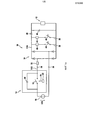
Вариант воплощения устройства 10 возбуждения для возбуждения нагрузки, в частности блока 12 СИД, схематически показан на Фиг. 1a. Устройство 10 возбуждения соединено с устройством 14 регулятора яркости света, которое соединено с внешним источником 16 напряжения, например, с внешним источником напряжения питающей сети, и адаптировано для обеспечения переменного напряжения V12 фазовой отсечки из напряжения V10 питания переменного тока. Устройство 14 регулятора яркости света содержит двунаправленный переключатель 18 и блок 22 управления для управления переключателем 18. Устройство 14 регулятора яркости света преобразует напряжение питания V10 переменного тока в напряжение V12 фазовой отсечки, путем переключения переключателя 18 и размыкания соединения между внешним источником 16 напряжения и выходным контактом устройства 14 регулятора яркости света. Устройство 14 регулятора яркости света дополнительно содержит конденсатор 26, подключенный параллельно к переключателю 18. Блок 22 управления управляет переключателем 18 посредством управляющего сигнала 24, чтобы обеспечивать сигнал V12 фазовой отсечки по заднему фронту.An embodiment of a
Блок 22 управления содержит схему синхронизации, которая требует обнаружения переходов через ноль для перезапуска таймера при каждом пересечении ноля напряжения V10 питающей сети для поддержания надлежащей работы устройства 14 регулятора яркости света.The control unit 22 includes a synchronization circuit, which requires the detection of zero crossings to restart the timer each time the zero voltage V10 of the supply network is crossed in order to maintain proper operation of the light
Устройство 10 возбуждения содержит первый входной контакт 28 и второй входной контакт 30, для соединения устройства 10 возбуждения с внешним источником 16 напряжения. Первый входной контакт 28 соединен с выходным контактом устройства 14 регулятора яркости света для приема напряжение V12 фазовой отсечки. Второй входной контакт 30 соединен с нейтральной линией внешнего источника 16 напряжения. Устройство 10 возбуждения может содержать входной импеданс 32, соединенный с первым входным контактом 28. Входной импеданс 32 может быть образован резистором, индуктором, EMI-фильтром (фильтром электромагнитных помех), и т.п. Устройство 10 возбуждения содержит выпрямитель 34 для выпрямления напряжения V12 фазовой отсечки до выпрямленного напряжения V14. Устройство 10 возбуждения дополнительно содержит первый делитель 36 напряжения и второй делитель 38 напряжения. Каждый из делителей 36, 38 напряжения содержит резистор 40, 42 и управляемый переключатель 44, 46. Резисторы 40, 42 имеют разные сопротивления, причем первый делитель 36 напряжения содержит высокоомный резистор 40, а второй делитель 38 напряжения содержит низкоомный резистор 42. Делители 36, 38 напряжения применяют к выпрямленному напряжению V14 за счет переключения переключателей 44, 46, причем второй делитель 38 напряжения применяют, когда обнаружен переход через ноль для напряжения V10 питания, или когда напряжение V10 питающей сети падает ниже значения 50 В, и причем первый делитель 36 напряжения применяют, когда амплитуда напряжения сети питания падает ниже значения 200 В, что снижает рассеивание мощности в резисторе 42. Делители 36, 38 напряжения соединяют входные контакты 28, 30 друг с другом в течение некоторого периода времени для напряжения фазовой отсечки для адаптации устройства 10 возбуждения к устройству 14 регулятора яркости света, вследствие чего схема синхронизации устройства 14 регулятора яркости света функционирует, как требуется.The
Устройство 10 возбуждения дополнительно содержит диод 48 и конденсатор 50, причем конденсатор 50 подключен параллельно к блоку 12 СИД, для обеспечения соответствующего напряжения возбуждения для возбуждения нагрузки 12. Нагрузка 12 содержит СИД, включая линейный или переключаемый преобразователь постоянного тока для согласования напряжения СИД с напряжением конденсатора 50.The
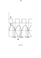
На Фиг. 1b показана блок-схема, иллюстрирующая форму волны напряжения для выпрямленного напряжения V14, соответствующего напряжению V10 питания (пунктирные линии), обеспечиваемого внешним источником 16 напряжения, и управляющий сигнал 24, обеспечиваемый блоком 22 управления, для управления переключателем 18 устройства 14 регулятора яркости света.In FIG. 1b is a block diagram illustrating a voltage waveform for a rectified voltage V14 corresponding to a supply voltage V10 (dashed lines) provided by an
Управляющий сигнал 24 отключает управляемый переключатель 18 и отсоединяет внешний источник 16 напряжения в момент времени t1. Выпрямленное напряжение V14 придерживается напряжения V10 питания до активации первого делителя 36 напряжения в момент времени t2. Выпрямленное напряжение V14 придерживается напряжения V10 питания, поскольку входной импеданс устройства 10 возбуждения велик по сравнению с импедансом конденсатора 26 устройства 14 регулятора яркости света. Поскольку конденсатор 26 разряжается в момент времени t1, а напряжение V10 прикладывают к контактам 28,30 через разряженный конденсатор 26, невозможно различить напряжение V12 фазовой отсечки и напряжение V10 питания до активации первого делителя 36 напряжения в момент времени t2. В момент времени t3, когда напряжение V14 понижается, например, ниже значения 50В, активируется второй делитель 38 напряжения. В момент времени t4, при обнаружении перехода через ноль напряжения V10 питания, управляющий сигнал 24 прикладывают для повторного замыкания управляемого переключателя 18 и для подачи напряжения V10 питания на выходное устройство 14 регулятора яркости света. Делители напряжения, как 36, так и 38, отключают в момент времени t4. Незначительное искажение выпрямленного напряжения V14 приводит к образованию нелинейности и мертвой зоне на кривой регулировки яркости света, поскольку фазовый угол напряжения V12 фазовой отсечки не может быть обнаружен. Компенсацию этой нелинейности можно преодолеть путем предварительного приложения слабого делителя 36 напряжения, однако, это может усилить рассеивание мощности устройства 10 возбуждения. Поэтому, для соответствующего возбуждения СИД необходимо обнаружить фазовый угол напряжения фазовой отсечки.The
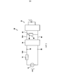
Фиг. 2 показывает устройство 60 возбуждения, включающее в себя блок 62 управления сигналами для управления выпрямленным напряжением V14. Основные элементы идентичны элементам на Фиг. 1 и обозначены идентичными ссылочными позициями. Здесь подробно разъясняются только различия.FIG. 2 shows an
Блок 62 управления сигналами подключен параллельно к выпрямителю 34. Выпрямитель 34 подключен к нагрузке 12 посредством соединительных элементов 63, 64. Блок 62 управления сигналами электрически соединен с соединительными элементами 63, 64. Выпрямитель 34 подает выпрямленное напряжение V14 на нагрузку 12 для возбуждения нагрузки 12.The
Блок 62 управления сигналами подключен к соединительным элементам 63, 64 и обеспечена подача электрического сигнала I на соединительные элементы 63, 64. Электрический сигнал I представляет собой электрический ток I, поступающий с электрического элемента 63. Электрический сигнал I обеспечивает понижение напряжения до выпрямленного напряжения V14, которое измеряют с помощью измерительного устройства 65 блока 62 управления сигналами, причем пиковое значение понижения напряжения зависит от состояния устройства 14 регулятора яркости света. Иными словами, пиковое значение понижения напряжения зависит от того, включен ли управляемый переключатель 18, и подается ли напряжение V10 питания на выпрямитель 34, или управляемый переключатель отключен, а конденсатор 26 устройства 14 регулятора яркости света подключен к выпрямителю 34. Электрический сигнал I подают в течение кратковременного интервала, предпочтительно, 50-100 мкс, на соединительный элемент 63. Если управляемый переключатель 18 устройства 14 регулятора яркости света включен, то пиковое значение понижения напряжения выпрямленного напряжения V14 мало. Если управляемый переключатель 18 устройства регулятора яркости света отключен, то пиковое значение понижения напряжения велико. Поэтому, блок 62 управления сигналами может обнаруживать состояние устройства 14 регулятора яркости света, и поэтому устройство 10 возбуждения может обнаруживать фазовый угол напряжения V12 фазовой отсечки за счет приложения электрического сигнала и измерения пикового значения возникающего понижения напряжения выпрямленного напряжения V14.The
Согласно одному варианту воплощения блок 62 управления сигналами содержит путь тока, включающий в себя низкое сопротивление, для соединения соединительных элементов 63, 64 друг с другом с обеспечением тока I и с возникновением понижения напряжения выпрямленного напряжения V14. Согласно другому варианту воплощения блок 62 управления сигналами содержит управляемый источник тока, направляющий ток I от соединительного элемента 63 к соединительному элементу 64, с возникновением понижения напряжения в выпрямленном напряжении V14. Согласно дополнительному варианту воплощения блок 62 управления сигналами содержит зарядный конденсатор, направляющий ток I от соединительного элемента 63 и обеспечивающий понижение напряжения в выпрямленном напряжении V14, как будет подробно описано в дальнейшем.According to one embodiment, the
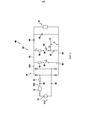
Фиг. 3 показывает устройство 60 возбуждения, включающее в себя блок 62 управления сигналами для управления выпрямленным напряжением V14 согласно предпочтительному варианту воплощения. Идентичные элементы обозначены идентичными ссылочными позициями, и здесь подробно разъяснены лишь различия.FIG. 3 shows an
Блок 62 управления сигналами соединен с соединительными элементами 63, 64, параллельно выпрямителю 34. Блок 62 управления сигналами содержит конденсатор 66, управляемый переключатель 68 и резистор 70. Конденсатор 66, управляемый переключатель 68 и резистор 70 последовательно соединены друг с другом. Управляемый переключатель 72 подключен параллельно конденсатору 66. Управляемый переключатель 72 обеспечен для соединения контактов конденсатора 66 друг с другом для разрядки конденсатора 66. Управляемым переключателем 68 управляют посредством управляющего сигнала 69. В ходе эксплуатации конденсатор 66 подключают параллельно выпрямителю 34 путем замыкания управляемого переключателя 68. Когда управляемый переключатель 68 замкнут, ток I заряжает конденсатор 66, и в выпрямленном напряжении V14 возникает понижение напряжения. Если управляемый переключатель 18 устройства 14 регулятора яркости света включен, и напряжение V10 питания подается к выпрямителю 34, ток зарядки I ограничен последовательным сопротивлением входного импеданса 32 и резистором 70 блока 62 управления сигналами. Поэтому, получается ограниченное малое пиковое значение понижения напряжения выпрямленного напряжения V14, соответствующее падению напряжения на входном импедансе 32. Если управляемый переключатель 18 отключен, напряжение на конденсаторе 66 определяется соотношением импеданса конденсатора 26 устройства регулятора яркости света и конденсатора 66 блока 62 управления сигналами. Если емкость конденсаторов 26, 66 идентична (например, составляет 100 нФ), то выпрямленное напряжение V14 падает приблизительно до 50%. Поэтому, значительное понижение напряжения выпрямленного напряжения V14 может быть обеспечено, если устройство 14 регулятора яркости света отключено. Понижение напряжения выпрямленного напряжения V14 измеряют, когда управляемый переключатель 68 замыкается посредством схемы дифференциатора. Схема дифференциатора обнаруживает пиковое значение понижения напряжения и, следовательно, определяет, включен ли или отключен управляемый переключатель 18.The
Предпочтительно, чтобы управляемый переключатель 68 был замкнут в течение кратковременного интервала, например, 50-100 мкс. Управляемый переключатель 68 и управляемый переключатель 72 приводятся в действие поочередно, таким образом, чтобы один их управляемых переключателей 68, 72 был бы разомкнут, когда другой управляемый переключатель 68, 72 замкнут. Поскольку управляемый переключатель 72 соединяет соединительные элементы конденсатора 66 друг с другом, то конденсатор 66 разряжается посредством тока 12 разрядки, когда управляемый переключатель 68 разомкнут. Поэтому, обеспечивается, чтобы конденсатор 66 разряжался при разомкнутом управляемом переключателе 68 для отведения тока I от соединительного элемента 62.Preferably, the controlled
Для обнаружения фазового угла напряжения V12 фазовой отсечки, управляемый переключатель 68 можно замыкать часто или раз в полпериода напряжения V10 питания. Поскольку рассеивание мощности устройства 10 возбуждения с применением понижения напряжения к выпрямленному напряжению V14 повышается, понижение напряжения генерируют, предпочтительно, только раз в полпериода напряжения V10 питания. Для обнаружения фазового угла напряжения V12 фазовой отсечки, момент времени, когда генерируется понижение напряжения, смещают от одного полупериода напряжения V10 питания к другому, как будет описано ниже.To detect the phase angle of the phase-cut voltage V12, the controlled
Фиг. 4 показывает диаграмму, иллюстрирующую форму волны напряжения выпрямленного напряжения V14, абсолютное значение напряжения V10 питания и управляющий сигнал 69 для управления управляемым переключателем 68.FIG. 4 shows a diagram illustrating the waveform of the voltage of the rectified voltage V14, the absolute value of the supply voltage V10, and the
Управляющий сигнал 69 для замыкания управляемого переключателя 68 обеспечивается для некоторых кратковременных интервалов для соединения конденсатора 66 с выпрямителем 34 и для обеспечения тока I. Продолжительность управления импульсами управляющего сигнала 69 составляет менее 1/10 от полуцикла входного напряжения V12, например, менее 200 мкс. При каждом управляющем импульсе управляющего сигнала 69, выпрямленное напряжение V14 показывает малое понижение напряжения 74 в течение интервала времени перед отключением устройства 14 регулятора яркости света в момент времени t1. После отключения устройства 14 регулятора яркости света в момент времени t1 путем размыкания управляемого переключателя 18, пиковое значение понижения напряжения возрастает, вследствие чего выпрямленное напряжение V14 падает приблизительно до 50%. Большое пиковое значение этого понижения напряжения 75 может быть легко обнаружено посредством схемы дифференциатора.The
Поэтому, фазовый угол напряжения V12 фазовой отсечки может быть легко обнаружен путем создания понижения напряжения в выпрямленном напряжении V14, и, соответственно, блок 12 СИД может быть возбужден.Therefore, the phase angle of the phase-cut voltage V12 can be easily detected by creating undervoltage in the rectified voltage V14, and accordingly, the
Потеря энергии за управляющий импульс определяется по электроэнергии, хранящейся в конденсаторе 66, и зависит от напряжения на конденсаторе 66. Напряжение на конденсаторе 66 ограничено постоянной времени сопротивления резистора 70 и емкостью конденсатора 66. Для снижения потери энергии устройства 10 возбуждения электрический сигнал I может быть обеспечен блоком 62 управления сигналами только раз за полуцикл напряжения V10 питания.The energy loss per control pulse is determined from the electric energy stored in the
Фиг. 5 показывает схематическую блок-схему блока поиска для обнаружения фазового угла напряжения V12 фазовой отсечки, в целом обозначенного ссылочной позицией 80. Блок 80 поиска содержит устройство 82 алгоритма поиска, детектор 84 перехода через ноль и дифференциатор 86. Каждый из детектора 84 перехода через ноль и дифференциатора 86 измеряет выпрямленное напряжение V14. Детектор 84 перехода через ноль обнаруживает переход через ноль выпрямленного напряжения V14 и подает соответствующий сигнал на устройство 82 алгоритма поиска. Дифференциатор 86 обнаруживает любые изменения выпрямленного напряжения V14, включая понижения 74, 75 напряжения, вызываемые электрическим сигналом I. Дифференциатор 86 обеспечивает информацию о том, обнаружено ли большое понижение 75 напряжения или малое понижение 74 напряжения для устройства 82 алгоритма поиска, посредством управляющего сигнала. Устройство 82 алгоритма поиска обеспечивает управляющий сигнал 69 или, как правило, управляющий сигнал 69 для управления блоком управления посредством сигналов 62 и для подачи соответствующего электрического сигнала I на соединительные элементы 63, 64. Устройство 82 алгоритма поиска обеспечивает короткие управляющие импульсы для создания понижения 74, 75 напряжения в выпрямленном напряжении V14. Если большое понижение 75 напряжения, т.е., срез по заднему фронту напряжения V12 фазовой отсечки, не обнаружено дифференциатором 86, то устройство 82 алгоритма поиска смещает управляющий импульс в следующем полуцикле выпрямленного напряжения V14 на более поздний момент времени для обнаружения фазового угла напряжения V12 фазовой отсечки. Если обнаружено большое понижение 75 напряжения, то алгоритм поиска смещает управляющий импульс в следующем полуцикле выпрямленного напряжения V14 на более ранний момент времени для более точного определения фазового угла. Поэтому, для точного определения фазового угла алгоритм сводится к 5-10 полуциклам (с точностью до 3-5°) выпрямленного напряжения V14. Блок 80 поиска может быть образован в виде цифровой интегральной схемы, такой как микроконтроллер.FIG. 5 shows a schematic block diagram of a search unit for detecting a phase angle of a phase-cut voltage V12, generally designated 80. The
Тогда как изобретение было проиллюстрировано и подробно описано на чертежах и в вышеприведенном описании, такую иллюстрацию и описание следует рассматривать как иллюстративные или примерные, а не ограничивающие; изобретение не ограничено раскрытыми вариантами воплощения. Другие модификации раскрытых вариантов воплощения могут быть поняты и осуществлены специалистами в данной области техники при реализации заявленного изобретения, из исследования чертежей, раскрытия и прилагаемой формулы изобретения.While the invention has been illustrated and described in detail in the drawings and in the above description, such illustration and description should be considered as illustrative or exemplary, and not limiting; the invention is not limited to the disclosed embodiments. Other modifications of the disclosed embodiments may be understood and carried out by those skilled in the art in the practice of the claimed invention, from examination of the drawings, disclosure and appended claims.
В формуле изобретения слово «содержащий» не исключает наличия других элементов или этапов, а элемент в единственном числе не исключает наличия множества элементов. Одиночный элемент или другой блок может выполнять функции нескольких единиц, перечисленных в формуле изобретения. Сам факт, что определенные меры перечислены во взаимно различных зависимых пунктах формулы изобретения, не указывает на то, что невозможно успешно использовать сочетание этих мер.In the claims, the word “comprising” does not exclude the presence of other elements or steps, and the singular element does not exclude the presence of a plurality of elements. A single element or other block may fulfill the functions of several units listed in the claims. The fact that certain measures are listed in mutually different dependent claims does not indicate that it is not possible to successfully use a combination of these measures.
Компьютерная программа может быть установлена/распространена на подходящем носителе, таком как оптический носитель данных или твердотельный носитель данных, поставляемый вместе с другим оборудованием, или как его часть, но также может распространяться в других формах, например, через Интернет или другие проводные или беспроводные телекоммуникационные системы.The computer program may be installed / distributed on a suitable medium, such as an optical data medium or a solid-state data medium supplied with other equipment, or as part of it, but can also be distributed in other forms, for example, via the Internet or other wired or wireless telecommunications system.
Никакие ссылочные позиции в формуле изобретения не должны рассматриваться как ограничивающие его объем.No reference position in the claims should not be construed as limiting its scope.
Claims (26)
Applications Claiming Priority (3)
| Application Number | Priority Date | Filing Date | Title |
|---|---|---|---|
| US201261593378P | 2012-02-01 | 2012-02-01 | |
| US61/593,378 | 2012-02-01 | ||
| PCT/IB2013/050468 WO2013114242A1 (en) | 2012-02-01 | 2013-01-18 | Driver device and driving method for driving a load, in particular in led unit comprising one or more leds |
Publications (2)
| Publication Number | Publication Date |
|---|---|
| RU2014135413A RU2014135413A (en) | 2016-03-27 |
| RU2665463C2 true RU2665463C2 (en) | 2018-08-30 |
Family
ID=47827395
Family Applications (1)
| Application Number | Title | Priority Date | Filing Date |
|---|---|---|---|
| RU2014135413A RU2665463C2 (en) | 2012-02-01 | 2013-01-18 | Driver device and driving method for driving load, in particular in led unit comprising one or more leds |
Country Status (6)
| Country | Link |
|---|---|
| US (1) | US9743467B2 (en) |
| EP (1) | EP2810532B1 (en) |
| JP (1) | JP6407724B2 (en) |
| CN (1) | CN104115559B (en) |
| RU (1) | RU2665463C2 (en) |
| WO (1) | WO2013114242A1 (en) |
Families Citing this family (19)
| Publication number | Priority date | Publication date | Assignee | Title |
|---|---|---|---|---|
| US11131431B2 (en) | 2014-09-28 | 2021-09-28 | Jiaxing Super Lighting Electric Appliance Co., Ltd | LED tube lamp |
| EP2810533B1 (en) * | 2012-02-02 | 2015-08-05 | Koninklijke Philips N.V. | Led light source |
| EP2802191B1 (en) * | 2013-05-07 | 2023-08-16 | Goodrich Lighting Systems GmbH | Dimmable led light unit and method of replacing a light unit |
| EP2802192B1 (en) * | 2013-05-10 | 2019-07-03 | Goodrich Lighting Systems GmbH | LED light unit and method of operating an LED light unit |
| US9369048B2 (en) * | 2014-04-22 | 2016-06-14 | Power Integrations, Inc. | Dimming edge detection for power converter |
| US9629207B2 (en) * | 2014-09-15 | 2017-04-18 | Dialog Semiconductor Inc. | Solid state lamp control |
| US9438122B2 (en) | 2014-11-10 | 2016-09-06 | Power Integrations, Inc. | Phase angle detection module for power converter |
| US9897265B2 (en) | 2015-03-10 | 2018-02-20 | Jiaxing Super Lighting Electric Appliance Co., Ltd. | LED tube lamp having LED light strip |
| GB2597856B (en) | 2015-12-18 | 2022-07-20 | Southwire Co Llc | Cable integrated solar inverter |
| EP3412117B1 (en) * | 2016-02-05 | 2020-08-19 | Schreder | Lamp control module consisting of base and control parts, communicating via nfc |
| DE102016217747B4 (en) * | 2016-09-16 | 2024-02-22 | Tridonic Gmbh & Co Kg | METHOD FOR BIDIRECTIONAL COMMUNICATION CENTER PHASE CUT MODULATION OF AN AC SUPPLY VOLTAGE AND CORRESPONDINGLY DESIGNED OPERATING DEVICE, CONTROL DEVICE AND SYSTEM |
| US10993297B2 (en) * | 2016-12-13 | 2021-04-27 | Koito Manufacturing Co., Ltd. | Lighting circuit and vehicular lamp |
| US11251621B1 (en) | 2017-08-03 | 2022-02-15 | Southwire Company, Llc | Solar power generation system |
| US11438988B1 (en) * | 2017-08-11 | 2022-09-06 | Southwire Company, Llc | DC power management system |
| US10582598B1 (en) * | 2017-11-02 | 2020-03-03 | Katerra Inc. | Light emitting diode activation control |
| CN109041331B (en) * | 2018-07-06 | 2020-05-12 | 矽力杰半导体技术(杭州)有限公司 | Reset current control circuit, control method and LED drive circuit |
| US11191136B2 (en) | 2018-07-16 | 2021-11-30 | Jiaxing Super Lighting Electric Appliance Co., Ltd. | LED lighting system, apparatus, and dimming method |
| US11071178B2 (en) | 2018-07-16 | 2021-07-20 | Jiaxing Super Lighting Electric Appliance Co., Ltd. | LED lighting system, apparatus, and dimming method |
| CN108848598B (en) * | 2018-08-31 | 2024-04-12 | 厦门市必易微电子技术有限公司 | Bleeder module for silicon controlled rectifier dimmer, LED driving circuit and driving method |
Citations (4)
| Publication number | Priority date | Publication date | Assignee | Title |
|---|---|---|---|---|
| EP2257124A1 (en) * | 2009-05-29 | 2010-12-01 | Nxp B.V. | Circuit for connecting a low current lighting circuit to a dimmer |
| WO2011008635A1 (en) * | 2009-07-14 | 2011-01-20 | Iwatt Inc. | Adaptive dimmer detection and control for led lamp |
| RU2009140317A (en) * | 2007-04-02 | 2011-05-10 | Конинклейке Филипс Электроникс Н.В. (Nl) | LED MANAGEMENT |
| US20110309759A1 (en) * | 2006-01-20 | 2011-12-22 | Exclara Inc. | Adaptive Current Regulation for Solid State Lighting |
Family Cites Families (17)
| Publication number | Priority date | Publication date | Assignee | Title |
|---|---|---|---|---|
| JPS646768A (en) * | 1987-06-29 | 1989-01-11 | Nikon Corp | Signal-level detection circuit |
| JPH0566235A (en) * | 1991-09-06 | 1993-03-19 | Hitachi Shonan Denshi Co Ltd | Peak holding circuit, peak detecting circuit and peak-position detecting circuit |
| KR101249025B1 (en) | 2004-10-22 | 2013-03-29 | 코닌클리즈케 필립스 일렉트로닉스 엔.브이. | Method for driving a led based lighting device |
| JP2009009760A (en) * | 2007-06-26 | 2009-01-15 | Toshiba Lighting & Technology Corp | Illumination device |
| WO2009004563A1 (en) | 2007-07-02 | 2009-01-08 | Philips Intellectual Property & Standards Gmbh | Driver device for a load and method of driving a load with such a driver device |
| WO2009085244A1 (en) * | 2007-12-21 | 2009-07-09 | Cypress Semiconductor Corporation | Controlling a light emitting diode fixture |
| US8013544B2 (en) | 2008-12-10 | 2011-09-06 | Linear Technology Corporation | Dimmer control leakage pull down using main power device in flyback converter |
| CN101902851A (en) * | 2009-05-25 | 2010-12-01 | 皇家飞利浦电子股份有限公司 | Light-emitting diode driving circuit |
| US8729729B2 (en) * | 2009-06-18 | 2014-05-20 | Mikhail Fridberg | Method and apparatus for driving low-power loads from AC sources |
| CN102474931B (en) | 2009-06-29 | 2015-07-15 | 皇家飞利浦电子股份有限公司 | Driver for cooperating with a wall dimmer |
| BR112012011642A2 (en) | 2009-11-19 | 2020-03-31 | Koninklijke Philips Electronics N. V. | DEVICE FOR THE DETECTION OF A DIMMER PHASE ANGLE ESTABLISHED BY THE OPERATION OF A DIMMER FOR A SOLID STATE LIGHTING LOAD AND METHOD FOR THE DETECTION OF A DIMMER PHASE ANGLE ESTABLISHED BY A DIMMER DETERMINATION OF DIMMER DETERMINATION |
| US8102683B2 (en) * | 2010-02-09 | 2012-01-24 | Power Integrations, Inc. | Phase angle measurement of a dimming circuit for a switching power supply |
| JP5031865B2 (en) * | 2010-03-23 | 2012-09-26 | シャープ株式会社 | LED drive circuit, LED illumination lamp, LED illumination device, and LED illumination system |
| CN102238774B (en) | 2010-04-30 | 2016-06-01 | 奥斯兰姆有限公司 | Angle of flow acquisition methods and device, and LED driving method and device |
| US8436548B2 (en) * | 2010-05-27 | 2013-05-07 | Osram Sylvania Inc. | Dimmer conduction angle detection circuit and system incorporating the same |
| EP2752088B1 (en) | 2011-09-06 | 2018-06-20 | Philips Lighting Holding B.V. | Power control unit and method for controlling electrical power provided to a load, in particular an led unit, and voltage control unit for controlling an output voltage of a converter unit |
| TWI489911B (en) * | 2011-12-30 | 2015-06-21 | Richtek Technology Corp | Active bleeder circuit triggering triac in all phase and light emitting device power supply circuit and triac control method using the active bleeder circuit |
-
2013
- 2013-01-18 WO PCT/IB2013/050468 patent/WO2013114242A1/en active Application Filing
- 2013-01-18 EP EP13707716.0A patent/EP2810532B1/en active Active
- 2013-01-18 RU RU2014135413A patent/RU2665463C2/en active
- 2013-01-18 JP JP2014555348A patent/JP6407724B2/en active Active
- 2013-01-18 CN CN201380007633.9A patent/CN104115559B/en not_active Expired - Fee Related
- 2013-01-18 US US14/375,180 patent/US9743467B2/en active Active
Patent Citations (4)
| Publication number | Priority date | Publication date | Assignee | Title |
|---|---|---|---|---|
| US20110309759A1 (en) * | 2006-01-20 | 2011-12-22 | Exclara Inc. | Adaptive Current Regulation for Solid State Lighting |
| RU2009140317A (en) * | 2007-04-02 | 2011-05-10 | Конинклейке Филипс Электроникс Н.В. (Nl) | LED MANAGEMENT |
| EP2257124A1 (en) * | 2009-05-29 | 2010-12-01 | Nxp B.V. | Circuit for connecting a low current lighting circuit to a dimmer |
| WO2011008635A1 (en) * | 2009-07-14 | 2011-01-20 | Iwatt Inc. | Adaptive dimmer detection and control for led lamp |
Also Published As
| Publication number | Publication date |
|---|---|
| CN104115559B (en) | 2017-05-10 |
| EP2810532B1 (en) | 2019-05-22 |
| US9743467B2 (en) | 2017-08-22 |
| US20150002040A1 (en) | 2015-01-01 |
| WO2013114242A1 (en) | 2013-08-08 |
| EP2810532A1 (en) | 2014-12-10 |
| JP6407724B2 (en) | 2018-10-17 |
| CN104115559A (en) | 2014-10-22 |
| JP2015509275A (en) | 2015-03-26 |
| RU2014135413A (en) | 2016-03-27 |
Similar Documents
| Publication | Publication Date | Title |
|---|---|---|
| RU2665463C2 (en) | Driver device and driving method for driving load, in particular in led unit comprising one or more leds | |
| RU2606387C2 (en) | Power control unit and method for controlling electrical power provided to a load, in particular a led unit, and voltage control unit for controlling an output voltage of a converter unit | |
| US10159126B2 (en) | LED based lighting application | |
| US9544962B2 (en) | Driver device and driving method for driving an LED unit | |
| RU2609130C2 (en) | Driver for connecting light-emitting diode to electronic ballast | |
| US10356867B2 (en) | Light-dimming device | |
| US9544966B2 (en) | Driver device and driving method for driving a load, in particular a LED unit | |
| US20240032175A1 (en) | Method and system for reducing flickering-of lamps powered by an electricity distribution network | |
| BE1019523A5 (en) | ZERO TRANSACTION DETECTOR, USE OF SUCH DETECTOR AND DIMMER INCLUDING SUCH DETECTOR. | |
| US10070488B2 (en) | Power converter between halogen transformer and LED |
Legal Events
| Date | Code | Title | Description |
|---|---|---|---|
| HZ9A | Changing address for correspondence with an applicant | ||
| PD4A | Correction of name of patent owner |