RU2606502C2 - Device and method for controlling current to solid state lighting circuit - Google Patents
Device and method for controlling current to solid state lighting circuit Download PDFInfo
- Publication number
- RU2606502C2 RU2606502C2 RU2013133905A RU2013133905A RU2606502C2 RU 2606502 C2 RU2606502 C2 RU 2606502C2 RU 2013133905 A RU2013133905 A RU 2013133905A RU 2013133905 A RU2013133905 A RU 2013133905A RU 2606502 C2 RU2606502 C2 RU 2606502C2
- Authority
- RU
- Russia
- Prior art keywords
- current
- capacitor
- led
- circuit
- transistor
- Prior art date
Links
Images
Classifications
-
- H—ELECTRICITY
- H05—ELECTRIC TECHNIQUES NOT OTHERWISE PROVIDED FOR
- H05B—ELECTRIC HEATING; ELECTRIC LIGHT SOURCES NOT OTHERWISE PROVIDED FOR; CIRCUIT ARRANGEMENTS FOR ELECTRIC LIGHT SOURCES, IN GENERAL
- H05B45/00—Circuit arrangements for operating light-emitting diodes [LED]
- H05B45/30—Driver circuits
- H05B45/395—Linear regulators
- H05B45/397—Current mirror circuits
-
- H—ELECTRICITY
- H05—ELECTRIC TECHNIQUES NOT OTHERWISE PROVIDED FOR
- H05B—ELECTRIC HEATING; ELECTRIC LIGHT SOURCES NOT OTHERWISE PROVIDED FOR; CIRCUIT ARRANGEMENTS FOR ELECTRIC LIGHT SOURCES, IN GENERAL
- H05B45/00—Circuit arrangements for operating light-emitting diodes [LED]
- H05B45/30—Driver circuits
- H05B45/355—Power factor correction [PFC]; Reactive power compensation
-
- H—ELECTRICITY
- H05—ELECTRIC TECHNIQUES NOT OTHERWISE PROVIDED FOR
- H05B—ELECTRIC HEATING; ELECTRIC LIGHT SOURCES NOT OTHERWISE PROVIDED FOR; CIRCUIT ARRANGEMENTS FOR ELECTRIC LIGHT SOURCES, IN GENERAL
- H05B45/00—Circuit arrangements for operating light-emitting diodes [LED]
- H05B45/50—Circuit arrangements for operating light-emitting diodes [LED] responsive to malfunctions or undesirable behaviour of LEDs; responsive to LED life; Protective circuits
- H05B45/59—Circuit arrangements for operating light-emitting diodes [LED] responsive to malfunctions or undesirable behaviour of LEDs; responsive to LED life; Protective circuits for reducing or suppressing flicker or glow effects
-
- Y—GENERAL TAGGING OF NEW TECHNOLOGICAL DEVELOPMENTS; GENERAL TAGGING OF CROSS-SECTIONAL TECHNOLOGIES SPANNING OVER SEVERAL SECTIONS OF THE IPC; TECHNICAL SUBJECTS COVERED BY FORMER USPC CROSS-REFERENCE ART COLLECTIONS [XRACs] AND DIGESTS
- Y02—TECHNOLOGIES OR APPLICATIONS FOR MITIGATION OR ADAPTATION AGAINST CLIMATE CHANGE
- Y02B—CLIMATE CHANGE MITIGATION TECHNOLOGIES RELATED TO BUILDINGS, e.g. HOUSING, HOUSE APPLIANCES OR RELATED END-USER APPLICATIONS
- Y02B20/00—Energy efficient lighting technologies, e.g. halogen lamps or gas discharge lamps
- Y02B20/30—Semiconductor lamps, e.g. solid state lamps [SSL] light emitting diodes [LED] or organic LED [OLED]
Abstract
Description
Область техники, к которой относится изобретениеFIELD OF THE INVENTION
Настоящее изобретение относится в общем к управлению твердотельными осветительными устройствами. Более конкретно различные способы и устройства согласно изобретению, описанные в настоящем документе, относятся к управлению коэффициентом мощности и эффективностью формирователя сигнала питания для устройства освещения.The present invention relates generally to the management of solid state lighting devices. More specifically, the various methods and devices according to the invention described herein relate to controlling the power factor and efficiency of a power driver for a lighting device.
Уровень техникиState of the art
Цифровые технологии освещения, т.е. освещение, основанное на полупроводниковых источниках света, таких как светоизлучающие диоды (LED), представляют собой конкурентоспособную альтернативу обычным флуоресцентным лампам, газоразрядным лампам высокой интенсивности (HID) и лампам накаливания. Функциональные преимущества и полезные эффекты LED включают в себя высокий уровень преобразования энергии и оптическую эффективность, долговечность, сниженные эксплуатационные затраты и многое другое. Недавние достижения в технологии LED обеспечили эффективные и надежные источники освещения с полным спектром, которые реализуют разнообразные световые эффекты во многих применениях. Некоторые из осветительных приборов, реализующих такие источники, имеют осветительный модуль, включающий в себя один или более LED, способные производить различные цвета, например красный, зеленый и синий, а также процессор для независимого управления производительностью LED для формирования различных цветов и световых эффектов с изменением цвета, например, как подробно описано в патентах США № 6,016,038 и 6,211,626.Digital lighting technology i.e. Lighting based on semiconductor light sources such as light emitting diodes (LEDs) is a competitive alternative to conventional fluorescent lamps, high intensity discharge lamps (HIDs) and incandescent lamps. Functional advantages and beneficial effects of LEDs include high levels of energy conversion and optical efficiency, durability, reduced operating costs and much more. Recent advances in LED technology have provided efficient and reliable full-spectrum lighting sources that realize a variety of lighting effects in many applications. Some of the lighting devices that implement such sources have a lighting module that includes one or more LEDs capable of producing various colors, for example red, green and blue, as well as a processor for independently controlling LED performance to produce different colors and lighting effects with changing colors, for example, as described in detail in US Pat. Nos. 6,016,038 and 6,211,626.
Обычно осветительный элемент на основе LED или нагрузка LED, которая включает в себя множество источников света на основе LED, такая как цепочка последовательно соединенных LED, управляется преобразователем мощности, который принимает напряжение и ток от источника питания-электросети. В качестве альтернативы, для снижения стоимости формирователя сигнала питания нагрузка LED может приводиться в действие непосредственно от источника питания-электросети, включая работу от переменного и постоянного тока. Однако приведение в действие переменным током непосредственно от источника питания-электросети имеет недостатки. Например, форма волны тока, подаваемого в нагрузку LED, имеет высокое пиковое значение по сравнению со средним значением. Таким образом, нагрузка LED приводится в действие со сниженной эффективностью из-за спада, а также из-за низкого коэффициента мощности. Кроме того, протекание тока возможно только когда мгновенное напряжение сети выше, чем прямое напряжение нагрузки LED. Поэтому могут быть относительно длительные периоды, в которые ток не течет в цепочку LED и не вырабатывается свет, что вызывает мерцание.Typically, an LED-based lighting element or LED load, which includes a plurality of LED-based light sources, such as a series of LEDs connected in series, is controlled by a power converter that receives voltage and current from a power source. Alternatively, to reduce the cost of the power driver, the LED load can be driven directly from the power supply, including mains AC and DC. However, AC driving directly from a power supply network has drawbacks. For example, the waveform of the current supplied to the LED load has a high peak value compared to the average value. Thus, the LED load is driven with reduced efficiency due to recession and also due to low power factor. In addition, current flow is only possible when the instantaneous mains voltage is higher than the forward LED load voltage. Therefore, there may be relatively long periods in which current does not flow into the LED circuit and light is not generated, which causes flickering.
Для частичного решения этих вопросов между источником питания-электросетью и осветительным элементом может быть подсоединена схема выпрямителя, а параллельно с нагрузкой LED в пределах осветительного элемента может быть соединен конденсатор. Например, на Фиг. 1 показана принципиальная схема обычного осветительного элемента 100 на основе LED, который включает в себя мостовую схему 110 выпрямителя, нагрузку 160 LED и конденсатор 141, который действует в качестве элемента управления коэффициентом мощности (PFC), и сглаживающую схему 140. Конденсатор 141 параллельно соединен с нагрузкой LED 160, которая включает в себя резистор 163, последовательно соединенный с цепочкой из одного или более источников света типа LED, указанной в виде LED 161 и 162. Мостовая схема 110 выпрямителя соединена с источником 101 питания - электросетью через резистор 105 и включает в себя диоды 111-114. Таким образом, мостовая схема 110 выпрямителя выдает выпрямленное напряжение электросети или входное напряжение Urect в схему 140.To partially solve these issues, a rectifier circuit can be connected between the power supply network and the lighting element, and a capacitor can be connected in parallel with the LED load within the lighting element. For example, in FIG. 1 is a circuit diagram of a conventional LED-based
Однако вследствие формы волны зарядки и разрядки тока IC конденсатора, подаваемого в конденсатор 141, и формы волны напряжения электросети осветительный элемент 100 на основе LED обычно потребляет ток, например, для перезарядки конденсатора 141 в течение относительно короткого периода времени, что приводит к высоким пиковым значениям тока и низкому коэффициенту мощности. Кроме того, главным образом резистор 105, соединенный с источником 101 питания-электросетью, ограничивает как повторную, так и исходную зарядку конденсатора 141. Поэтому при исходном включении нагрузки 160 LED может иметь место избыточный пусковой ток. Например, если нагрузку 160 LED включают при пиковом значении напряжения электросети источника 101 питания-электросети, ток IC конденсатора 141 может иметь относительно высокое значение по сравнению с работой в номинальном режиме. В результате, если нагрузка 160 LED не включает в себя несколько источников света, последовательно соединенных с одной схемой, что приводит к относительно низкому значению номинального рабочего тока LED за счет дополнительных компонентов осветительного элемента 100 на основе LED, даже относительно малого числа источников света будет достаточно для того, чтобы привести в действие магнитный расцепитель разъединителя цепи. Таким образом, число осветительных блоков 100 на основе LED, которые могут быть соединены в одну схему, может быть значительно меньшим (например, лишь 1/10 или даже 1/50) по сравнению с тем, которое можно ожидать в соответствии с номинальным значением тока.However, due to the waveform of charging and discharging the current I C of the capacitor supplied to the
С точки зрения эффективности и при рассмотрении отдельного источника света на основе LED форма волны тока не представляет собой проблему. Однако при рассмотрении большого числа источников света на основе LED высокие значения тока в короткий интервал времени вносят искажения в электросети питания и могут привести в действие разъединитель цепи (например, привести в действие быстродействующий магнитный расцепитель разъединителя цепи). Из-за искажения тока сети питания использование нагрузок LED с очень низкими коэффициентами мощности запрещено правилами. Например, в Европе минимальный требуемый коэффициент мощности может составлять 0,5, что может быть обеспечено с использованием вышеописанного решения, основанного на выпрямителе и конденсаторе. Однако в других регионах требуются относительно высокие значения коэффициента мощности, такие как 0,7 или выше, например 0,9.In terms of efficiency and when considering a separate LED-based light source, the current waveform is not a problem. However, when considering a large number of LED-based light sources, high currents in a short period of time introduce distortions into the power supply network and can trigger a circuit disconnector (for example, actuate a high-speed magnetic trip of a circuit disconnector). Due to the distortion of the power supply current, the use of LED loads with very low power factors is prohibited by the rules. For example, in Europe, the minimum required power factor may be 0.5, which can be achieved using the above solution based on the rectifier and capacitor. However, in other regions, relatively high power factor values, such as 0.7 or higher, for example 0.9, are required.
Таким образом, в данной области техники существует потребность в обеспечении приведения в действие переменным током осветительных элементов на основе LED непосредственно от источника питания-электросети, при этом поддерживая относительно высокие коэффициенты мощности. Кроме того, в данной области техники существует потребность в исключении избыточных значений пускового тока при исходном включении осветительных элементов на основе LED, приводимых в действие непосредственно от источника питания-электросети.Thus, in the art there is a need to provide alternating current driving of LED-based lighting elements directly from a power supply network while maintaining relatively high power factors. In addition, in the art there is a need to eliminate excessive inrush current values when initially turning on LED-based lighting elements that are driven directly from a power source.
Сущность изобретенияSUMMARY OF THE INVENTION
Настоящее описание относится к устройствам и способам согласно изобретению, использующим источник динамически модулированного тока, соединенный последовательно с конденсатором в осветительном элементе LED для формирования тока конденсатора, повышая таким образом коэффициент мощности осветительного элемента LED, при этом повышая или доводя до максимального значения эффективность, а также снижая импульсную рассеиваемую мощность в источнике тока. Кроме того, источник модулированного тока ограничивает входной ток, не позволяя осветительному элементу LED привести в действие разъединитель цепи.The present description relates to devices and methods according to the invention, using a dynamically modulated current source connected in series with a capacitor in the LED lighting element to generate a capacitor current, thereby increasing the power factor of the LED lighting element, while increasing or maximizing the efficiency, as well as reducing pulsed power dissipation in the current source. In addition, the modulated current source limits the input current, preventing the LED lighting element from activating the circuit breaker.
В общем, в одном аспекте предложено устройство управления током для твердотельной осветительной нагрузки, причем устройство включает в себя конденсатор и источник тока. Конденсатор соединен в параллельном соединении с твердотельной осветительной нагрузкой. Источник тока последовательно соединен с параллельным соединением конденсатора и твердотельной осветительной нагрузки, причем источник тока выполнен с возможностью динамической модуляции амплитуды входного тока, подаваемого в параллельное соединение конденсатора и твердотельной осветительной нагрузки, на основании входного напряжения.In general, in one aspect, there is provided a current control device for a solid state lighting load, the device including a capacitor and a current source. The capacitor is connected in parallel with a solid-state lighting load. The current source is connected in series with the parallel connection of the capacitor and the solid-state lighting load, the current source being configured to dynamically modulate the amplitude of the input current supplied to the parallel connection of the capacitor and the solid-state lighting load based on the input voltage.
В другом аспекте предложено устройство управления током для светодиодной (LED) нагрузки, причем устройство включает в себя конденсатор, транзистор и схему управления модуляцией. Конденсатор параллельно соединен нагрузкой LED. Транзистор последовательно соединен между конденсатором и мостовой схемой выпрямителя, обеспечивающей выпрямленное входное напряжение. Схема управления модуляцией соединена параллельно с конденсатором и транзистором и выполнена с возможностью приема выпрямленного входного напряжения из мостовой схемы выпрямителя. Схема управления модуляцией включает в себя токовое зеркало, соединенное с затвором транзистора, причем токовое зеркало активируется и деактивируется по выбору для модуляции с понижением и повышением амплитуды тока через конденсатор на основании входного напряжения от мостовой схемы выпрямителя.In another aspect, there is provided a current control device for an LED load, the device including a capacitor, a transistor, and a modulation control circuit. The capacitor is connected in parallel by the LED load. The transistor is connected in series between the capacitor and the rectifier bridge circuit, providing a rectified input voltage. The modulation control circuit is connected in parallel with the capacitor and transistor and is configured to receive the rectified input voltage from the bridge rectifier circuit. The modulation control circuit includes a current mirror connected to the gate of the transistor, the current mirror being activated and deactivated optionally for modulation with decreasing and increasing the amplitude of the current through the capacitor based on the input voltage from the rectifier bridge circuit.
В другом аспекте предложен способ управления током для твердотельной осветительной нагрузки. Способ включает в себя этапы, на которых принимают входное напряжение, имеющее форму волны; и регулируют модуляцию амплитуды тока конденсатора для конденсатора, соединенного параллельно с твердотельной осветительной нагрузкой, в ответ на, по меньшей мере, одно из формы волны принятого входного напряжения и временной задержки формы волны принятого входного напряжения. При регулировке модуляции амплитуды тока конденсатора изменяют, по меньшей мере, одно из коэффициента мощности и эффективности работы твердотельной осветительной нагрузки.In another aspect, a method for controlling current for a solid state lighting load is provided. The method includes the steps of taking an input voltage in the form of a wave; and adjusting the modulation of the amplitude of the capacitor current for the capacitor connected in parallel with the solid-state lighting load in response to at least one of the waveform of the received input voltage and the time delay of the waveform of the received input voltage. When adjusting the modulation, the amplitudes of the capacitor current change at least one of the power factor and the efficiency of the solid-state lighting load.
В контексте настоящего документа, в целях настоящего описания понятие «LED» следует понимать как включающее в себя любой электролюминесцентный диод или другой вид системы на основе инжекции носителей/перехода, способной формировать излучение в ответ на электрический сигнал. Таким образом, понятие LED включает в себя, не ограничиваясь, различные полупроводниковые структуры, которые испускают свет в ответ на ток, светоизлучающие полимеры, органические светоизлучающие диоды (OLED), электролюминесцентные полосы и тому подобное. В частности, понятие LED относится к светоизлучающим диодам всех видов (включая полупроводниковые и органические светоизлучающие диоды), которые могут быть выполнены с возможностью формирования излучения в одном или более из инфракрасного спектра, ультрафиолетового спектра и различных участков видимого спектра (включая, в общем, излучения с длиной волны от приблизительно 400 нанометров до приблизительно 700 нанометров). Некоторые примеры LED включают в себя, не ограничиваясь, различные виды LED инфракрасного излучения, LED ультрафиолетового излучения, LED красного свечения, LED синего свечения, LED зеленого свечения, LED желтого свечения, LED янтарного свечения, LED оранжевого свечения и LED белого свечения (дополнительно описаны ниже). Также следует понимать, что LED могут быть конфигурированы и/или управляемы для формирования излучения, имеющего различные значения ширины спектральной полосы (например, полную ширину на половине максимума или FWHM) для конкретного спектра (например, малую ширину спектральной полосы, большую ширину спектральной полосы), и различные преобладающие значения длины волны в пределах конкретной общей категоризации цвета.In the context of this document, for the purposes of the present description, the concept of "LED" should be understood as including any electroluminescent diode or other type of system based on the injection of carriers / transition, capable of generating radiation in response to an electrical signal. Thus, the concept of LED includes, but is not limited to, various semiconductor structures that emit light in response to current, light emitting polymers, organic light emitting diodes (OLED), electroluminescent strips, and the like. In particular, the concept of LED refers to light emitting diodes of all kinds (including semiconductor and organic light emitting diodes), which can be configured to generate radiation in one or more of the infrared spectrum, the ultraviolet spectrum and various parts of the visible spectrum (including, in general, radiation with a wavelength of from about 400 nanometers to about 700 nanometers). Some examples of LEDs include, but are not limited to, various types of LED infrared, LED UV, LED red, LED blue, LED green, LED yellow, LED amber, LED orange and white LED (further described below). It should also be understood that LEDs can be configured and / or controlled to generate radiation having different spectral bandwidths (e.g., full width at half maximum or FWHM) for a particular spectrum (e.g., small spectral bandwidth, large spectral bandwidth) , and various prevailing wavelengths within a particular general color categorization.
Например, один вариант реализации LED, выполненного с возможностью формирования по существу белого цвета (например, LED белого свечения) может включать в себя несколько кристаллов, которые соответственно испускают различные спектры электролюминесценции, которые в сочетании смешиваются для формирования по существу белого цвета. В другом варианте реализации LED белого свечения может быть связан с люминесцентным материалом, который преобразует электролюминесценцию, имеющую первый спектр, в другой, второй спектр. В одном примере данного варианта реализации электролюминесценция с относительно малой длиной волны и малой шириной спектральной полосы «накачивает» люминесцентный материал, который, в свою очередь, испускает излучение с большей длиной волны, имеющее несколько более широкий спектр.For example, one embodiment of an LED configured to produce substantially white color (e.g., a white LED) may include several crystals that respectively emit different electroluminescence spectra that are combined to form a substantially white color. In another embodiment, a white LED may be associated with a luminescent material that converts electroluminescence having a first spectrum into another, second spectrum. In one example of this embodiment, electroluminescence with a relatively short wavelength and a small spectral bandwidth “pumps” luminescent material, which, in turn, emits radiation with a longer wavelength, which has a slightly wider spectrum.
Также следует понимать, что понятие LED не ограничивает физические и/или электрические виды сборки LED. Например, как описано выше, LED может означать одиночное светоизлучающее устройство, имеющее множество кристаллов, которые выполнены с возможностью соответственно испускать излучение в различных спектрах (например, которые могут или не могут быть управляемыми по отдельности). Также LED может быть связан с люминесцентным материалом, который рассматривается в качестве неотъемлемой части LED (например, некоторые виды LED белого свечения). В общем, понятие LED может относиться к LED в корпусе, LED без корпуса, LED поверхностного монтажа, LED для монтажа на плате, LED с Т-образным корпусом, LED с корпусом с радиальными выводами, к LED в рассеивающем большую мощность корпусе, LED, включающим в себя какой-либо корпусный и/или оптический элемент (например, рассеивающую линзу) и т.п.It should also be understood that the concept of LED does not limit the physical and / or electrical forms of LED assembly. For example, as described above, an LED may mean a single light emitting device having a plurality of crystals that are configured to respectively emit radiation in different spectra (for example, which may or may not be individually controlled). LED can also be associated with a luminescent material, which is considered as an integral part of LEDs (for example, some types of white LEDs). In general, the concept of LED can refer to LED in a housing, LED without a housing, LED for surface mounting, LED for mounting on a board, LED with a T-shaped housing, LED with a housing with radial terminals, LED in a high power dissipating housing, LED, including any housing and / or optical element (for example, a scattering lens), etc.
Понятие «источник света» следует понимать как относящееся к одному или более из различных источников излучения, включая, но не ограничиваясь, источники на основе LED (включающие в себя один или более LED, как определено выше), источники с элементом накаливания (например, лампы накаливания, галогеновые лампы), флуоресцентные источники, фосфоресцирующие источники, источники на основе разряда высокой интенсивности (например, натриевые, ртутные и металлогалоидные лампы), лазеры, другие виды электролюминесцентных источников, пиролюминесцентные источники (например, факел), свечелюминесцентные источники (например, калильные сетки, угольные дуговые источники излучения), фотолюминесцентные источники (например, газоразрядные источники), источники с катодной люминесценцией, использующие электронное насыщение, гальванолюминесцентные источники, кристаллолюминесцентные источники, кинелюминесцентные источники, термолюминесцентные источники, триболюминесцентные источники, сонолюминесцентные источники, радиолюминесцентные источники и люминесцентные полимеры.The term "light source" should be understood as referring to one or more of various radiation sources, including, but not limited to, LED-based sources (including one or more LEDs, as defined above), incandescent sources (for example, lamps incandescent, halogen lamps), fluorescent sources, phosphorescent sources, sources based on a high-intensity discharge (for example, sodium, mercury and metal halide lamps), lasers, other types of electroluminescent sources, pyroluminescent sources (e.g., torch), candle-luminescent sources (e.g., glow grids, carbon arc radiation sources), photoluminescent sources (e.g., gas-discharge sources), electron-saturated cathode luminescence sources, galvanoluminescent sources, crystal-luminescent sources, cine-luminescent sources, thermoluminescent sources triboluminescent sources, sonoluminescent sources, radioluminescent sources and luminescent polymers.
Конкретный источник света может быть выполнен с возможностью формирования электромагнитного излучения в пределах видимого спектра, за пределами видимого спектра или в сочетании обоих упомянутых спектров. Таким образом, понятия «свет» и «излучение» используются в настоящем документе взаимозаменяемо. Кроме того, источник света может в качестве неотъемлемого компонента включать в себя один или более фильтров (например, цветные фильтры), линзы или другие оптические компоненты. Также следует понимать, что источники света могут быть конфигурированы для различных применений, включая, но не ограничиваясь, индикацию, отображение и/или освещение. «Источник освещения» представляет собой источник света, который, в частности, выполнен с возможностью формирования излучения, имеющего достаточную интенсивность для эффективного освещения внутреннего или наружного пространства. В данном контексте «достаточная интенсивность» подразумевает достаточную мощность излучения в видимом спектре, формируемого в пространстве или окружении (для обозначения общего светового выхода источника света во всех направлениях с точки зрения мощности излучения или «светового потока» часто используется единица «люмен») для обеспечения окружающего освещения (то есть света, который может восприниматься опосредованно и может, например, отражаться от одной или более из различных лежащих на его пути поверхностей перед тем, как он будет полностью или частично воспринят).A particular light source may be configured to generate electromagnetic radiation within the visible spectrum, outside the visible spectrum, or in a combination of both of these spectra. Thus, the concepts of “light” and “radiation” are used interchangeably herein. In addition, the light source may, as an integral component, include one or more filters (eg, color filters), lenses, or other optical components. It should also be understood that light sources can be configured for various applications, including, but not limited to, display, display, and / or lighting. A “light source” is a light source which, in particular, is configured to generate radiation having sufficient intensity to effectively illuminate an indoor or outdoor space. In this context, “sufficient intensity” means sufficient radiation power in the visible spectrum formed in space or surroundings (the unit “lumen” is often used to indicate the total light output of a light source in all directions from the point of view of radiation power or “light flux”) ambient lighting (that is, light that can be perceived indirectly and can, for example, be reflected from one or more of the different surfaces lying in its path before it is fully or partially perceived).
Понятие «спектр» следует понимать как подразумевающее одну или более частот (или длин волн) излучения, вырабатываемого одним или более источниками света. Соответственно, понятие «спектр» подразумевает частоты (или длины волн) не только в видимом диапазоне, но также частоты (или длины волн) в инфракрасном, ультрафиолетовом и других частях общего спектра электромагнитных излучений. Также конкретный спектр может иметь относительно малую ширину спектральной полосы (например, FWHM, имеющую по существу мало частотных составляющих или составляющих по длине волны) или относительно большую ширину спектральной полосы (несколько частотных составляющих или составляющих по длине волны, имеющих разную относительную интенсивность). Также следует понимать, что конкретный спектр может быть результатом смешивания двух или более других спектров (например, смешивания излучения, соответственно испускаемого множеством источников света).The concept of “spectrum” should be understood as implying one or more frequencies (or wavelengths) of radiation generated by one or more light sources. Accordingly, the concept of “spectrum” means frequencies (or wavelengths) not only in the visible range, but also frequencies (or wavelengths) in the infrared, ultraviolet, and other parts of the general spectrum of electromagnetic radiation. Also, a particular spectrum may have a relatively small spectral bandwidth (e.g., FWHM having substantially few frequency or wavelength components) or a relatively large spectral bandwidth (several frequency or wavelength components having different relative intensities). It should also be understood that a particular spectrum may be the result of mixing two or more other spectra (for example, mixing radiation, respectively emitted by multiple light sources).
Понятие «осветительный прибор» используется в настоящем документе для обозначения варианта реализации или конфигурации одного или более осветительных элементов с конкретным формфактором, компоновкой или сборкой. Понятие «осветительный элемент» используется в настоящем документе для обозначения устройства, включающего в себя один или более источников света одного и того же вида или различных видов. Конкретный осветительный элемент может иметь одну из различных конфигураций монтажа для источника(ов) света, конфигураций и форм оболочки/корпуса и/или конфигураций электрического и механического соединения. Кроме того, конкретный осветительный элемент может при необходимости быть связан с (например, включать в себя, быть соединенным и/или находиться в одной сборке с) различными другими компонентами (например, с управляющей схемой), относящимися к работе источника(ов) света. «Осветительный элемент на основе LED» обозначает осветительный элемент, который включает в себя один или более источников света на основе LED, описанных выше, по отдельности или в сочетании с другими источниками света не на основе LED. «Многоканальный» осветительный элемент относится к осветительному элементу на основе LED или не на основе LED, который включает в себя по меньшей мере два источника света, выполненных с возможностью соответственно формировать излучение в различных спектрах, причем каждый различный спектр источника может называться «каналом» многоканального осветительного элемента.The term “lighting fixture” is used herein to indicate an embodiment or configuration of one or more lighting elements with a specific form factor, layout, or assembly. The term “lighting element” is used herein to refer to a device including one or more light sources of the same kind or different kinds. A particular lighting element may have one of various mounting configurations for the light source (s), configurations and shapes of the shell / housing and / or configurations of the electrical and mechanical connection. In addition, a particular lighting element may, if necessary, be associated with (for example, include, be connected to and / or be in the same assembly with) various other components (for example, with a control circuit) related to the operation of the light source (s). “LED-based lighting element” means a lighting element that includes one or more LED-based light sources described above, individually or in combination with other non-LED-based light sources. A "multi-channel" lighting element refers to an LED or non-LED-based lighting element that includes at least two light sources configured to respectively generate radiation in different spectra, each different source spectrum being referred to as a "multi-channel" channel lighting element.
Понятие «контроллер» используется в настоящем документе в общем для описания различных устройств, относящихся к работе одного или более источников света. Контроллер может быть реализован множеством способов (например, такой как специализированное аппаратное обеспечение) для выполнения различных функций, описанных в настоящем документе. «Процессор» представляет собой один пример контроллера, который использует один или более микропроцессоров, которые могут быть запрограммированы с использованием программного обеспечения (например, микропрограммы) для выполнения различных функций, описанных в настоящем документе. Контроллер может быть реализован с использованием или без использования процессора и также может быть реализован в виде сочетания специализированного аппаратного обеспечения для выполнения некоторых функций и процессора (например, одного или более запрограммированных микропроцессоров и связанной с ним схемы) для выполнения других функций. Примеры компонентов контроллера, которые могут быть использованы в различных вариантах выполнения настоящего изобретения включают в себя, не ограничиваясь, обычные микропроцессоры, специализированные интегральные схемы (ASIC) и программируемые логические интегральные схемы (FPGA).The term “controller” is used throughout this document to describe various devices related to the operation of one or more light sources. A controller may be implemented in a variety of ways (e.g., such as specialized hardware) to perform various functions described herein. A “processor” is one example of a controller that uses one or more microprocessors that can be programmed using software (eg, microprograms) to perform the various functions described herein. A controller may be implemented with or without a processor and may also be implemented as a combination of specialized hardware to perform certain functions and a processor (for example, one or more programmed microprocessors and an associated circuit) to perform other functions. Examples of controller components that can be used in various embodiments of the present invention include, but are not limited to, conventional microprocessors, application specific integrated circuits (ASICs), and programmable logic integrated circuits (FPGAs).
В различных вариантах реализации процессор или контроллер могут быть связаны с одним или более запоминающим носителем (называемым в общем «запоминающим устройством», например энергозависимым и энергонезависимым компьютерным запоминающим устройством, таким как RAM, PROM, EPROM и EEPROM, гибкие диски, компакт-диски, оптические диски, магнитная лента и т.д.). В некоторых вариантах реализации запоминающий носитель может быть кодирован одной или более программами, которые при выполнении в одном или более процессорах и/или контроллерах выполняют по меньшей мере некоторые из функций, описанных в настоящем документе. Различные запоминающие носители могут быть закреплены в процессоре или контроллере или могут быть переносными таким образом, что одна или более программ, сохраненных в них, могут быть загружены в процессор или контроллер для реализации различных аспектов настоящего изобретения, описанного в настоящем документе. Понятия «программа» или «компьютерная программа» используются в настоящем документе в общем смысле для обозначения любого вида компьютерного кода (например, программного обеспечения или микропрограммы), которые могут быть использованы для программирования одного или более процессоров или контроллеров.In various embodiments, the processor or controller may be associated with one or more storage media (referred to generally as a “storage device”, for example volatile and non-volatile computer storage devices such as RAM, PROM, EPROM and EEPROM, floppy disks, CDs, optical disks, magnetic tape, etc.). In some embodiments, the storage medium may be encoded by one or more programs that, when executed on one or more processors and / or controllers, perform at least some of the functions described herein. Various storage media may be attached to a processor or controller, or may be portable, such that one or more programs stored therein can be downloaded to a processor or controller to implement various aspects of the present invention described herein. The terms “program” or “computer program” are used herein in a general sense to mean any kind of computer code (eg, software or firmware) that can be used to program one or more processors or controllers.
Понятие «адресуемый» используется в настоящем документе для обозначения устройства (например, источника света в общем, осветительного элемента или прибора, контроллера или процессора, связанного с одним или более источников света или осветительных элементов, других устройств, не относящихся с освещению и т.п.), которое выполнено с возможностью приема информации (например, данных), предназначенной для множества устройств, включающих в себя данное устройство, и для реагирования по выбору на конкретную информацию, предназначенную для него. Понятие «адресуемый» часто используется в связи с сетевым окружением (или «сетью», дополнительно описанной ниже), в котором множество устройств соединены вместе какой-либо средой или средами связи.The term “addressable” is used herein to mean a device (for example, a light source in general, a lighting element or device, controller or processor associated with one or more light sources or lighting elements, other devices not related to lighting, etc. .), which is configured to receive information (eg, data) intended for a plurality of devices including this device, and to optionally respond to specific information intended for it. The term “addressable” is often used in connection with a network environment (or “network”, further described below), in which a plurality of devices are connected together by any medium or communication medium.
В одном сетевом варианте реализации одно или более устройств, соединенных с сетью, могут служить в качестве контроллера для одного или более других устройств, соединенных с сетью (например, в отношениях «главный/подчиненный»). В другом варианте реализации сетевое окружение может включать в себя один или более специализированных контроллеров, которые выполнены с возможностью управления одним или более устройствами, соединенными с сетью. В общем, каждое из множества устройств, соединенных с сетью, может иметь доступ к данным, которые имеются в средстве или средствах связи; однако конкретное устройство может быть «адресуемым», поскольку оно выполнено с возможностью по выбору обмениваться данными (например, принимать данные и/или передавать данные) с сетью на основании, например, одного или более конкретных назначенных ему идентификаторов (например, «адресов»).In one network embodiment, one or more devices connected to the network can serve as a controller for one or more other devices connected to the network (for example, in a master / slave relationship). In another embodiment, the network environment may include one or more specialized controllers that are configured to control one or more devices connected to the network. In general, each of a plurality of devices connected to a network may have access to data that is available in the medium or means of communication; however, a particular device may be “addressable” because it is configured to optionally exchange data (eg, receive data and / or transmit data) with the network based on, for example, one or more specific identifiers assigned to it (eg, “addresses”) .
Понятие «сеть» в контексте настоящего документа относится к любой взаимосвязи двух или более устройств (включая контроллеры или процессоры), которая способствует переносу информации (например, для управления устройством, хранения данных, обмена данными и т.п.) между любыми двумя или более устройствами и/или среди множества устройств, соединенных с сетью. Как следует понимать, различные варианты реализации сетей, подходящих для соединения между собой множества устройств, могут включать в себя любую из различных сетевых топологий и использовать любой из различных протоколов связи. Кроме того, в различных сетях согласно настоящему описанию любое соединение между двумя устройствами может представлять специализированное соединение между двумя системами или, в качестве альтернативы, неспециализированное соединение. В дополнение к переносу информации, предназначенной для двух устройств, такое неспециализированное соединение может переносить информацию, не обязательно предназначенную для какого-либо из двух устройств (например, открытое сетевое соединение). Кроме того, следует понимать, что различные сети устройств, описанные в настоящем документе, могут использовать одно или более беспроводных, проводных/кабельных и/или оптоволоконных соединений, способствующих переносу информации по сети.The term "network" in the context of this document refers to any relationship between two or more devices (including controllers or processors) that facilitates the transfer of information (for example, to control a device, store data, exchange data, etc.) between any two or more devices and / or among a plurality of devices connected to a network. As should be understood, various network implementations suitable for connecting multiple devices to each other may include any of various network topologies and use any of various communication protocols. In addition, in various networks, as described herein, any connection between two devices may represent a specialized connection between two systems or, alternatively, a non-specialized connection. In addition to transferring information intended for two devices, such a non-specialized connection may carry information not necessarily intended for either of the two devices (for example, an open network connection). In addition, it should be understood that the various device networks described herein may use one or more wireless, wired / cable and / or fiber-optic connections to facilitate the transfer of information over the network.
Понятие «пользовательский интерфейс» в контексте настоящего документа означает интерфейс между пользователем или оператором-человеком и одним или более устройств, который обеспечивает возможность связи между пользователем и устройством(ами). Примеры таких пользовательских интерфейсов, которые могут быть использованы в различных вариантах реализации настоящего изобретения, включают в себя, не ограничиваясь, переключатели, потенциометры, клавиши, диски, ползунки, мышь, клавиатуру, кнопочную панель, различные виды игровых устройств управления (например, джойстики), шаровые манипуляторы, экраны отображения, различные виды графических пользовательских интерфейсов (GUI), сенсорные экраны, микрофоны и другие виды датчиков, которые могут принимать какую-либо форму формируемого человеком стимула и формировать сигнал в ответ.The term "user interface" in the context of this document means an interface between a user or human operator and one or more devices, which provides the possibility of communication between the user and device (s). Examples of such user interfaces that can be used in various embodiments of the present invention include, but are not limited to, switches, potentiometers, keys, disks, sliders, mouse, keyboard, keypad, various kinds of game control devices (e.g., joysticks) , trackballs, display screens, various kinds of graphical user interfaces (GUIs), touch screens, microphones and other types of sensors that can take any form of a formed person FROM stimulus and generate a signal in response.
Следует понимать, что все сочетания вышеприведенных подходов и дополнительные подходы, более подробно описанные ниже (при условии, что такие подходы не являются взаимно несовместимыми), рассматриваются как часть изобретения, описанного в настоящем документе. В частности, все сочетания признаков заявляемого изобретения, приведенные в конце настоящего описания, подразумеваются частью изобретения, раскрытого в настоящем документе. Также следует понимать, что терминологию, явным образом используемую в настоящем документе, которая также может быть приведена в любом описании, включенном в настоящий документ путем ссылки, следует понимать в значении, которое более всего соответствует конкретным подходам, раскрытым в настоящем документе.It should be understood that all combinations of the above approaches and additional approaches, described in more detail below (provided that such approaches are not mutually incompatible), are considered as part of the invention described herein. In particular, all combinations of features of the claimed invention given at the end of the present description are intended to be part of the invention disclosed herein. It should also be understood that the terminology explicitly used herein, which may also be given in any description incorporated herein by reference, should be understood in a meaning that is most consistent with the specific approaches disclosed herein.
Краткое описание чертежейBrief Description of the Drawings
На чертежах подобные ссылочные позиции в общем относятся к одним и тем же элементам на различных видах. Также чертежи не обязательно выполнены в масштабе, вместо чего основное внимание уделяется в общем иллюстрации принципов настоящего изобретения.In the drawings, like reference numerals generally refer to the same elements in different views. Also, the drawings are not necessarily drawn to scale, instead, the focus is generally on illustrating the principles of the present invention.
На Фиг. 1 приведена принципиальная схема обычного устройства управления током для схемы LED.In FIG. 1 is a schematic diagram of a conventional current control device for an LED circuit.
На Фиг. 2 приведена принципиальная схема устройства управления током для схемы LED согласно примерному варианту выполнения.In FIG. 2 is a circuit diagram of a current control device for an LED circuit according to an exemplary embodiment.
На Фиг. 3 приведена принципиальная схема устройства управления током для схемы LED согласно примерному варианту выполнения.In FIG. 3 is a circuit diagram of a current control device for an LED circuit according to an exemplary embodiment.
На Фиг. 4 приведена принципиальная схема устройства управления током для схемы LED согласно примерному варианту выполнения.In FIG. 4 is a circuit diagram of a current control device for an LED circuit according to an exemplary embodiment.
На Фиг. 5 показаны кривые входного тока и формы волны тока LED, обеспечиваемые устройством управления током для схемы LED согласно примерному варианту выполнения.In FIG. 5 shows input current curves and LED current waveforms provided by the current control device for the LED circuit according to an exemplary embodiment.
На Фиг. 6 приведен график, иллюстрирующий смоделированную работу устройства управления током для схемы LED согласно примерному варианту выполнения.In FIG. 6 is a graph illustrating simulated operation of a current control device for an LED circuit according to an exemplary embodiment.
Осуществление изобретенияThe implementation of the invention
Заявитель в общем осознал и оценил полезность поддержания высоких коэффициентов мощности и эффективности при приведении в действие осветительных элементов на основе LED непосредственно от источника питания-электросети. Кроме того, заявитель осознал и оценил полезность исключения избыточных пусковых токов при исходном включении осветительных элементов на основе LED, приводимых в действие непосредственно от источника питания-электросети.The applicant generally recognized and appreciated the usefulness of maintaining high power and efficiency factors when driving LED-based lighting elements directly from a power source. In addition, the applicant realized and appreciated the usefulness of eliminating excess inrush currents during the initial inclusion of LED-based lighting elements that are driven directly from a power source.
Ввиду вышесказанного, различные варианты выполнения и реализации настоящего изобретения относятся к формирователю сигнала питания для осветительного элемента на основе LED, который выполняет активное формирование над входным током. То есть формирователь сигнала питания включает в себя источник тока, который выполнен с возможностью динамической модуляции амплитуды входного тока в ответ на форму волны входного напряжения, хотя могут быть использованы и другие входные критерии. Например, амплитуду входного тока можно модулировать в ответ на временную задержку или сочетание временной задержки и формы волны входного напряжения, не выходя за рамки объема настоящего описания. Соответственно, ток конденсатора, соединенного параллельно с осветительным элементом на основе LED, является активно управляемым и формируемым для достижения значения, зависимого от времени или состояния. Применение другой формы волны тока (например, имеющей другие амплитуды) влияет на коэффициент мощности и электрическую эффективность осветительного элемента на основе LED таким образом, что источники света LED могут быть «настроены» на желаемый коэффициент мощности при сохранении высокой эффективности. Также может быть снижена импульсная рассеиваемая мощность в источнике тока. Приводное устройство может быть использовано, например, в модернизационных светодиодных лампах с малым потреблением мощности и модулях с более высокими коэффициентами мощности.In view of the foregoing, various embodiments and implementations of the present invention relate to a power driver for an LED-based lighting element that performs active shaping on the input current. That is, the power driver includes a current source that is capable of dynamically modulating the amplitude of the input current in response to the waveform of the input voltage, although other input criteria may be used. For example, the amplitude of the input current can be modulated in response to a time delay or a combination of time delay and the waveform of the input voltage, without going beyond the scope of the present description. Accordingly, the current of the capacitor connected in parallel with the LED-based lighting element is actively controlled and generated to achieve a value dependent on time or state. The use of a different current waveform (for example, having different amplitudes) affects the power factor and electrical efficiency of the LED-based lighting element in such a way that the LED light sources can be “tuned” to the desired power factor while maintaining high efficiency. The pulsed power dissipation in the current source may also be reduced. The drive unit can be used, for example, in modernization LED lamps with low power consumption and modules with higher power factors.
На Фиг. 2 приведена принципиальная схема устройства управления током для твердотельной осветительной нагрузки, такой как схема LED, согласно примерному варианту выполнения.In FIG. 2 is a circuit diagram of a current control device for a solid state lighting load, such as an LED circuit, according to an exemplary embodiment.
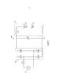
Как показано на Фиг. 2, осветительный элемент 200 на основе LED включает в себя мостовую схему 210 выпрямителя, схему 240 управления коэффициентом мощности (PFC) и сглаживания и нагрузку 260 LED. Мостовая схема 210 выпрямителя соединена с источником 201 питания-электросетью через резистор 205 и включает в себя диоды 211-214. Мостовая схема 210 выпрямителя, таким образом, выдает выпрямленное напряжение Urect электросети в схему 240 PFC и сглаживания. Как может быть очевидно специалисту в данной области техники, некоторые варианты реализации осветительного элемента 200 на основе LED также могут включать в себя дополнительные компоненты. Например, для соблюдения определенных нормативов по искажениям в электросети питания могут иметься элементы защиты от избыточного напряжения, такие как предохранители, конденсаторы фильтрации шума, средство тепловой защиты, интерфейсы связи и тому подобное. Однако эти дополнительные элементы не будут подробно описаны ради ясности описания.As shown in FIG. 2, the LED-based
Схема 240 PFC и сглаживания включает в себя источник 245 тока, конденсатор 241 и диод 242. Источник 245 тока последовательно соединен между положительным выходом мостовой схемы 210 выпрямителя и узлом N1 для приема выпрямленного входного напряжения Urect и выдачи тока IC конденсатора. Диод 242 параллельно соединен с источником 245 тока между положительным выходом мостовой схемы 210 выпрямителя и узлом N1. Диод 242 может быть, например, диодом Зенера и включен в схему для защиты источника 245 тока от перенапряжения. Например, без диода 242 большой всплеск напряжения (например, в несколько раз более высокий, чем нормальное выпрямленное напряжение Urect электросети) вызвал бы высокое напряжение в источнике 245 тока. На практике компоненты источника 245 тока (примеры которых описаны ниже со ссылкой на Фиг. 4) имеют ограничения по номинальному напряжению, и поэтому диод 242 выбирают таким образом, чтобы не превышать номинальное напряжение, установленное для этих компонентов. В одном варианте выполнения диод 242 не принимает на себя ток перенапряжения, а перегружает модуляцию источника 245 тока для активного сдерживания входного напряжения Urect. В данной ситуации ограничение входного тока обеспечивается главным образом резистором 205.The PFC and smoothing
Конденсатор 241 последовательно соединен между узлом N1 и землей и таким образом отделен от входа схемы 210 выпрямителя источником 245 тока. Конденсатор 241 также параллельно соединен с нагрузкой 260 LED, которая включает в себя резистор 263, полосу из одного или более источников света LED, представленную примерными LED 261 и 262. Нагрузка 260 LED соединена между узлом N1 и землей и таким образом соединена параллельно с конденсатором 241. В показанной конфигурации резистор 205 и источник 245 тока определяют величину входного тока IIn, поступающего от источника 201 питания-электросети, который обеспечивает соответственно ток IC конденсатора (то есть ток зарядки конденсатора и ток разрядки конденсатора) через конденсатор 241 и ток ILED LED через нагрузку 260 LED.A
Активное влияние источника 245 тока на ток IC конденсатора обеспечивает возможность формирования тока IC конденсатора и установки таким образом коэффициента мощности в схеме 240 PFC и сглаживания. Ток IC конденсатора не является фиксированным, а динамически изменяется в зависимости от времени и/или состояния. В самом деле, ввиду интегрирующего поведения конденсатора 241 в процесс может быть вовлечена некоторая временная составляющая. В данном примере ток IC конденсатора изменяется в соответствии с формой волны входного напряжения Urect от источника 201 питания-электросети и мостовой схемы 210 выпрямителя, хотя понятно, что ток IC конденсатора может в качестве альтернативы изменяться в соответствии с другими и/или дополнительными критериями, такими как временная задержка, как упоминалось выше. Например, измеряют мгновенное значение входного напряжения Urect и используют его в качестве управляющего сигнала для источника 245 тока. В ответ на форму волны входного напряжения Urect источник 245 тока модулирует амплитуду входного тока IIn, что приводит к соответствующей модуляции амплитуды тока, выдаваемого в параллельное соединение конденсатора 141 и нагрузки 260 LED, указываемого соответственно как ток IC конденсатора и ток ILED LED. В простом случае амплитуда входного тока IIn (начиная с заданного уровня) модулируется с повышением (увеличивается) или модулируется с понижением (уменьшается) в ответ на увеличения и уменьшения мгновенного входного напряжения Urect соответственно. При условии относительно стабильного значения тока ILED LED можно обнаружить, что эта модуляция является в высокой степени модуляцией тока IC конденсатора.Active influence on the
Кроме того, пусковой ток ILED LED для нагрузки 260 LED, то есть ток при исходном соединении нагрузки 260 LED с источником 201 питания-электросетью после предшествующего выключения, эффективным образом ограничен. То есть даже при запуске ток ILED LED ограничен номинальным значением, за счет чего полностью исключается эффект пускового тока. Эта активная функция ограничения тока является результатом того, что нагрузка 260 LED параллельно соединена с конденсатором 241. Во-первых, входной ток IIN в параллельное соединение конденсатора 241 и нагрузки 260 LED является ограниченным, и, во-вторых, конденсатор 241 действует как обход для более высокочастотных компонентов для нагрузки 260 LED. Поэтому нагрузка 260 LED эффективно защищена от пускового тока. Также ограничение входного тока IIN предотвращает приведение в действие разъединителей цепи, как упоминалось выше.In addition, the starting current I LED LED for the
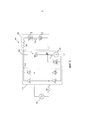
На Фиг. 3 приведена принципиальная схема устройства управления током для твердотельной осветительной нагрузки, такой как схема LED, согласно примерному варианту выполнения.In FIG. 3 is a circuit diagram of a current control device for a solid state lighting load, such as an LED circuit, according to an exemplary embodiment.
Как показано на Фиг. 3, осветительный элемент 300 на основе LED включает в себя мостовую схему 310 выпрямителя, схему 340 PFC и сглаживания и нагрузку 360 LED, которые аналогичны мостовой схеме 210 выпрямителя, схеме 240 PFC и сглаживания и нагрузке 260 LED, описанным выше со ссылкой на осветительный элемент 200 на основе LED. Однако схема 340 PFC и сглаживания по Фиг. 3 включает в себя источник 345 тока, конденсатор 341 и диод 342, причем источник 345 тока соединен с отрицательным выходом мостовой схемы 310 выпрямителя. Источник 345 тока последовательно соединен между узлом N2 и землей и управляет модуляцией тока IC конденсатора для конденсатора 341 и током ILED LED в ответ на форму волны входного напряжения Urect, как описано выше. В остальном конфигурация и работа осветительного элемента 300 на основе LED является по существу той же, что описана выше в отношении осветительного элемента 200 на основе LED. Диод 342 параллельно соединен с источником 345 тока между выходом на землю мостовой схемы 310 выпрямителя и узлом N2. Как описано выше, диод 342 может быть, например, диодом Зенера и включен в схему для защиты от перенапряжения источника 345 тока и нагрузки 360 LED.As shown in FIG. 3, the LED-based
На Фиг. 4 приведена принципиальная схема устройства управления током для твердотельной осветительной нагрузки, такой как схема LED, согласно примерному варианту выполнения. Более конкретно, на Фиг. 4 показан иллюстративный вариант реализации схемы PFC и сглаживания, обозначенной как схема 440 PFC и сглаживания, согласно примерному варианту выполнения.In FIG. 4 is a circuit diagram of a current control device for a solid state lighting load, such as an LED circuit, according to an exemplary embodiment. More specifically, in FIG. 4 shows an illustrative embodiment of a PFC and smoothing scheme designated as PFC and smoothing
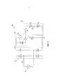
Как показано на Фиг. 4, осветительный элемент 400 на основе LED включает в себя мостовую схему 410 выпрямителя, схему 440 PFC и сглаживания и нагрузку 460 LED. Мостовая схема 410 выпрямителя соединена с источником 401 питания-электросетью через резистор 505 и включает в себя диоды 411-414. Мостовая схема 410 выпрямителя, таким образом, выдает выпрямленное напряжение Urect электросети в схему 440 PFC и сглаживания. Кроме того, Фиг. 4 включает в себя (факультативные) конденсаторы 406 и 407 переменного тока для демонстрации возможности изменения входного каскада. Хотя показаны два примерных конденсатора 406 и 407, следует понимать, что могут присутствовать один или более конденсаторов. Когда конденсаторы входного каскада не используются, входной ток электросети непосредственно подается в мостовой выпрямитель 410, как показано перемычкой X3.As shown in FIG. 4, the LED-based
Схема 440 PFC и сглаживания включает в себя источник 445 тока и конденсатор 441, причем источник 445 тока соединен с отрицательным выходом мостовой схемы 410 выпрямителя, как описано выше в отношении источника 345 тока, показанного на Фиг. 3. Однако следует понимать, что источник 445 тока по Фиг. 4 может, в качестве альтернативы, быть соединен с положительным выходом мостовой схемы 410 выпрямителя, как описано выше в отношении источника 245 тока, показанного на Фиг. 2, не выходя за рамки объема настоящего описания. Конденсатор 441 параллельно соединен с нагрузкой 460 LED, которая включает в себя резистор 463 и примерный источник 461 напряжения LED, соединенный последовательно.The PFC and smoothing
Источник 445 тока схемы 440 PFC и сглаживания включает в себя схему 471 источника тока и схему 472 опорного уровня. Схема 471 источника тока модулирует входной ток IIn и включает в себя переключатель или транзистор 442, последовательно соединенный между конденсатором 441 и землей. Транзистор 442 показан в виде полевого транзистора «металл-оксид-полупроводник» (MOSFET), хотя в схему могут быть включены и другие виды транзисторов, такие как биполярный плоскостной транзистор (BJT), не выходя за рамки объема настоящего описания. Схема 471 источника тока также включает в себя резистор 458, диод 448 и конденсатор 449, описанные ниже. Схема 472 опорного уровня определяет номинальный, немодулированный входной управляющий сигнал для схемы 471 источника тока и включает в себя резисторы 446 и 447 и диод 457, который может быть, например, диодом Зенера.The
Резистор 446 и диод 457 в общем формируют опорное напряжение, которое устанавливается посредством резистора 447, и входной управляющий сигнал схемы 471 источника тока. В частности, входной управляющий сигнал стробируют в транзистор 442 и схему 450 управления модуляцией, которая включает в себя токовое зеркало 459, которое активируется по выбору в ответ на работу перемычки X1. То есть когда перемычка X1 закрыта, а перемычка X2 открыта, токовое зеркало 459 активируется, что приводит к модуляции с понижением (более низкой амплитуде) входного тока IIn. Когда перемычка X2 закрыта, а перемычка X1 открыта, токовое зеркало 459 деактивируется и ток Imr приведет к модуляции с повышением (более высокой амплитуде) входного тока IIn.
Более конкретно, схема 450 управления модуляцией включает в себя резистор 453 и диод 456, который может быть диодом Зенера, последовательно соединенным между положительным выходом мостовой схемы 410 выпрямителя (для приема входного напряжения Urect) и узлом N1. Узел N1 соединен с землей через первую и вторую цепи. Первая цепь включает в себя резистор 454, по выбору последовательно соединенный с транзистором 451 токового зеркала 459 через первую перемычку X1. Вторая цепь включает в себя резистор 455, последовательно соединенный по выбору с транзистором 452 токового зеркала 459 через первую перемычку X2. Транзисторы 451 и 452 изображены как BJT в целях пояснения, но могут быть любым видом из различных видов транзисторов, включая, например, полевые транзисторы (FET), не выходя за рамки объема настоящего описания. Транзистор 451 имеет коллектор, соединенный с первой перемычкой X1, эмиттер, соединенный с землей, и базу, соединенную с коллектором транзистора 451 и с базой транзистора 452. Транзистор 452 имеет коллектор, соединенный со второй перемычкой X2, эмиттер, соединенный с землей, и базу, соединенную с базой и коллектором транзистора 451.More specifically, the
Что касается транзистора 442 схемы 471 источника тока, его затвор соединен с узлом N2, который является коллектором транзистора 452. Транзистор 442 дополнительно включает в себя сток, соединенный с конденсатором 441 через диод 444, и исток, соединенный с землей через резистор 458 токового шунта, который обеспечивает сопротивление токового шунта. Конденсатор 449 и диод 448, который может быть диодом Зенера, соединены параллельно друг другу между затвором и истоком транзистора 452. Кроме того, резистор 446 соединен между диодом 444 и узлом N3. Резистор 447 соединен между узлами N3 и N4, который является затвором транзистора 442. Диод 457, который может быть диодом Зенера, соединен между узлом N3 и землей. Следует отметить, что схема 440 PFC и сглаживания может также включать в себя диод защиты от перенапряжения, такой как диод 342 по Фиг. 3, который может быть соединен параллельно с транзистором 442, параллельно с последовательным соединением транзистора 442 и резистора 458, параллельно с резистором 446 или в любой другой конфигурации, подходящей для ограничения напряжения через транзистор 442. Однако ради ясности описания диод защиты от перенапряжения не показан на Фиг. 4.As for the
В показанной иллюстративной конфигурации напряжение затвора транзистора 442, напряжение UGS_442 «затвор-исток» транзистора 442 и резистор 458 определяют верхний предел тока через транзистор 442 и, таким образом, верхний предел входного тока IIn при нормальной работе, т.е. когда защита от чрезмерного напряжения не является активной. Напряжение UG_442 на затворе транзистора 442 обычно подается через диод 457 и резисторы 446 и 447. Поскольку затвор транзистора 442 в некоторой степени разъединен с напряжением диода 457 посредством резистора 447, существует возможность манипулирования напряжением UG_442 на затворе и, таким образом, входным током IIn. Входной ток IIn модулируют с повышением или понижением на определенное значение, когда входное напряжение Urect превышает пороговое значение напряжения, определяемое диодом 456. Как только пороговое значение напряжения превышено, выполняется модуляция с понижением через резистор 454 и активированное токовое зеркало 459 путем закрытия X1 и/или выполняется модуляция с повышением через резистор 455 путем закрытия второй перемычки X2.In the illustrated configuration shown, the gate voltage of the
В различных вариантах выполнения может осуществляться активное управление функциональностью, указанное на Фиг. 4 примерными перемычками X1 и X2. Например, X1 и X2 могут быть заменены управляемыми переключателями или другими средствами для активирования и деактивирования левой и правой цепей тока соответственно, не выходя за рамки объема настоящего описания. Состояние (например, уровень входного напряжения Urect), при котором активируется любая из модуляции с повышением и/или с понижением, может в таком случае быть выбрано посредством дополнительных элементов схемы (не показаны), таких как микропроцессор, процессор или контроллер.In various embodiments, the active functionality control described in FIG. 4 exemplary jumpers X1 and X2. For example, X1 and X2 can be replaced by controlled switches or other means to activate and deactivate the left and right current circuits, respectively, without departing from the scope of the present description. The state (for example, the input voltage level U rect ) at which any of the modulation is activated with increasing and / or decreasing, can then be selected by additional circuit elements (not shown), such as a microprocessor, processor or controller.
На Фиг. 4 показан универсальный вариант реализации, в котором возможны модуляции как с повышением, так и с понижением для обеспечения максимальной гибкости. Разумеется, могут быть предусмотрены альтернативные варианты реализации, обеспечивающие возможность только модуляции с повышением или с понижением, не выходя за рамки объема настоящего описания. Например, специализированный вариант выполнения, например предназначенный для определенного рынка с известными нормативами гармоник электросети, может требовать обеспечения только модуляции с повышением для достижения желаемого сочетания эффективности, коэффициента мощности и гармоник электросети. В таком случае, например, не будет необходимости в токовом зеркале 459.In FIG. Figure 4 shows a universal embodiment in which modulations are possible with both increase and decrease to provide maximum flexibility. Of course, alternative implementations may be provided, providing the possibility of only modulation with increasing or decreasing, without going beyond the scope of the present description. For example, a specialized embodiment, for example, designed for a specific market with well-known standards for harmonics of the mains, may require only modulation with increase to achieve the desired combination of efficiency, power factor and harmonics of the mains. In this case, for example, there will be no need for a
При необходимости большей гибкости, вместо извлечения сигнала модуляции с повышением или с понижением из общего сигнала напряжения, формируемого в узле N1 могут быть добавлены один или более диодов Зенера (не показаны), например, параллельно диоду 456, таким образом, чтобы уровень входного напряжения Urect, при котором начинается модуляция с повышением, отличался от уровня входного напряжения Urect, при котором начинается модуляция с понижением. В результате входной управляющий сигнал для схемы 471 источника тока может быть базовым опорным сигналом от схемы 472 опорного уровня до тех пор, пока входное напряжение Urect ниже какого-либо из пороговых значений. Входной управляющий сигнал модулируют с повышением, когда входное напряжение Urect выше первого порогового значения, но ниже второго порогового значения, и модулируют с понижением, когда входное напряжение Urect выше второго порогового значения. В данной конфигурации уровни первого и второго пороговых значений должны быть установлены соответственно (например, путем выбора надлежащих диодов), а «интенсивность» модулирующего сигнала определяется значениями резисторов 454, 455 и 447, участвующими в модуляции с повышением и с понижением, которые могут быть различными для обеспечения уникальных полезных эффектов для любой конкретной ситуации или для соответствия расчетным требованиям, предъявляемым конкретным применением в различных вариантах реализации, что очевидно специалисту в данной области техники.If more flexibility is needed, instead of extracting the modulation signal with increasing or decreasing voltage from the common voltage signal generated in node N1, one or more Zener diodes (not shown) can be added, for example, parallel to
В описанных вариантах выполнения токовое зеркало имеет соотношение 1:1 между токами на коллекторах транзисторов 451 и 452. Некоторое количество энергии, связанной с формированием тока на коллекторах из входного напряжения, может быть сэкономлено при использовании токового зеркала с другим соотношением, например при использовании большего числа транзисторов или других элементов схемы.In the described embodiments, the current mirror has a 1: 1 ratio between the currents on the collectors of
Обращаясь вновь к Фиг. 4, в качестве примера работы осветительного элемента 400 на основе LED можно предположить, что перемычка X1 закрыта, а перемычка X2 открыта, что обеспечивает возможность модуляции с понижением амплитуды входного тока IIn. В частности, исходный запрограммированный ток I0 показан в уравнении (1), где U457 - напряжение на диоде 457, UGS_442 - напряжение «затвор-исток» транзистора 442, и R458 - сопротивление резистора 458:Referring again to FIG. 4, as an example of the operation of the LED-based
![]()
![]()
С левой стороны токового зеркала 459 ток Iml транзистора 451 токового зеркала 459 показан в уравнении (2), где U456 - напряжение на диоде 456, UBE_452 - напряжение «база-эмиттер» транзистора 452, R453 - сопротивление резистора 453 и R454 - сопротивление резистора 454:On the left side of the
![]()
![]()
Как правило, значением UBE_452 в 0,7 В можно пренебречь. Вследствие конфигурации токового зеркала 459 то же значение тока Iml обеспечено с правой стороны токового зеркала 459 как ток Imr, которое равно току IC_452 на коллекторе транзистора 452. Ток IC_452 на коллекторе пропускают через разъединительный резистор 447, что приводит к пропорциональному падению напряжения. Таким образом, оставшееся напряжение UG_442 транзистора 442 снижается, и таким образом ограничивается оставшийся входной ток IIn, как показано в уравнении (3):As a rule, a value of U BE_452 of 0.7 V can be neglected. Due to the configuration of

Разумеется, подобное уравнение можно получить для модуляции с повышением, когда перемычка X1 открыта и перемычка X2 закрыта. Кроме того, значения различных составляющих, исходный (максимальный) входной ток In и степень модуляции с понижением могут быть различными, что обеспечивает уникальные полезные эффекты для любой конкретной ситуации или для соответствия расчетным требованиям, предъявляемым конкретным применением в различных вариантах реализации, что очевидно специалисту в данной области техники. Например, в целях иллюстрации, не ограничивающие значения различных компонентов по Фиг. 4 могут быть следующими: конденсаторы 406 и 407 могут иметь емкость 1000 нф и 680 нф соответственно, а резистор 405 может иметь сопротивление 100 Ом. В схеме 440 PFC и сглаживания конденсатор 441 может иметь емкость 5 мкф, конденсатор 449 может иметь емкость 1 нф, резистор 453 может иметь сопротивление 200 кОм, резистор 446 может иметь сопротивление 39 кОм, и резистор 447 может иметь сопротивление 22 кОм. Кроме того, транзисторы 451 и 452 токового зеркала могут представлять собой биполярные транзисторы обратной проводимости (NPN BJT), а транзистор 442 может представлять собой n-канальный полевой транзистор «металл-оксид-полупроводник» (NMOS MOSFET). В различных альтернативных конфигурациях транзисторы 451 и 452 могут быть биполярными транзисторами прямой проводимости (PNP BJT) и/или их коллекторы и эмиттеры могут быть инвертированы, а транзистор 442 может быть p-канальным полевым транзистором «металл-оксид-полупроводник» (PMOS MOSFET) и/или его исток и сток могут быть инвертированы. В нагрузке 460 LED резистор может иметь сопротивление 470 Ом, а источник 461 напряжения нагрузки LED может представлять собой последовательное соединение множества спаек LED, имеющих подходящее высокое прямое напряжение, например около от 60 до 130 В при работе от сети переменного тока 120 В. Источник 461 нагрузки LED включен для того, чтобы представлять общее поведение нагрузки LED, имеющей относительно ограниченный диапазон рабочего входного напряжения, например, по сравнению с резистором. И все же источник 461 напряжения нагрузки LED будет иметь некоторое резистивное поведение. Это резистивное поведение может быть достаточным для реализации функциональности, обозначенной резистором 463 на Фиг. 4, хотя также может иметь место случай, когда функциональность, обозначенная резистором 463, реализуется внутренним резистивным поведением источника 461 напряжения нагрузки LED и дополнительным сопротивлением (например, дорожки с сопротивлением на печатной плате или резистором).Of course, a similar equation can be obtained for modulation with increasing when jumper X1 is open and jumper X2 is closed. In addition, the values of the various components, the initial (maximum) input current In, and the degree of modulation with decreasing can be different, which provides unique useful effects for any particular situation or for meeting the design requirements for a particular application in various implementations, which is obvious to a specialist in this technical field. For example, for purposes of illustration, not limiting the values of the various components of FIG. 4 may be as follows:
Как указано выше, могут быть использованы и другие входные критерии кроме формы волны входного напряжения, такие как временная задержка или сочетание временной задержки и формы волны входного напряжения, не выходя за рамки объема настоящего описания. Например, источник тока может приводиться в действие в соответствии с формой волны, но с определенной временной задержкой. В примерной конфигурации временная задержка может быть реализована через задержку на резисторе/конденсаторе, например, включая конденсаторы 406 и 407 по Фиг. 4, или через реальную схему «записи и проигрывания» для регистрации формы волны за один цикл, ее смещения по времени и использования сигнала со смещением по времени для модуляции в более поздней части этого цикла или в любом последующем цикле.As indicated above, other input criteria can be used in addition to the input voltage waveform, such as a time delay or a combination of time delay and input voltage waveform, without departing from the scope of the present description. For example, a current source may be driven in accordance with a waveform, but with a specific time delay. In an exemplary configuration, the time delay can be realized through the delay on the resistor / capacitor, for example, including
На Фиг. 5 показаны кривые входного тока и формы волны тока LED, обеспечиваемые устройством управления током в схеме LED согласно примерному варианту выполнения.In FIG. 5 shows input current curves and LED current waveforms provided by the current control device in the LED circuit according to an exemplary embodiment.
Как показано на Фиг. 5, кривая 515 показывает форму волны примерного входного тока IIn, а кривая 525 показывает результирующую форму волны примерного тока ILED LED, где схема 440 PFC и сглаживания обеспечивает интенсивную модуляцию с понижением. Например, кривая 525 может получиться, когда перемычка X1 закрыта и перемычка X2 открыта, активируя токовое зеркало 459 схемы 440 PFC и сглаживания. Полезный эффект модуляции с понижением заключается в уменьшении тока при максимальной разности напряжений между входным напряжением Urect и напряжением конденсатора на транзисторе 442. Эта разность напряжений представляет собой напряжение отпускания на источнике 445 тока, которое в большой степени является напряжением на транзисторе 442. При снижении входного тока IIn при таком высоком уровне входного напряжения Urect рассеивание энергии на источнике 445 тока ограничено и таким образом повышается эффективность. Разумеется, некоторое среднее значение входного тока IIn должно быть подано на нагрузку 460 LED. Более высокий входной ток IIn при более низких уровнях входного напряжения Urect обеспечивает более высокое значение тока зарядки (тока IC конденсатора) для конденсатора 441 для достижения желаемого уровня среднего тока ILED LED в нагрузку 460 LED. При такой модуляции с понижением повышается эффективность, а пиковая тепловая нагрузка (термическое напряжение) источника 445 тока полезным образом снижается. Кроме того, уменьшается мерцание нагрузки 460 LED, поскольку общая зарядка конденсатора 441 эффективным образом разбивается на две части, что приводит к уменьшению пульсации напряжения на конденсаторе 441 и таким образом к уменьшенной пульсации тока ILED LED. Кроме того, пульсация тока ILED LED содержит более высокочастотные составляющие, к которым менее чувствителен человеческий глаз.As shown in FIG. 5,
На Фиг. 6 приведен график, иллюстрирующий смоделированную работу устройства управления током в схеме LED согласно примерному варианту выполнения. В частности, на Фиг. 6 показаны рабочие точки (например, включая один или более конденсаторов 460, 407 на стороне переменного тока) в диапазоне от эффективности около 92 процентов при коэффициенте мощности около 0,58 до эффективности около 75 процентов при коэффициенте мощности около 0,85, обозначенные черными ромбами. Дополнительные модели работы показывают рабочие точки (например, без конденсаторов на стороне переменного тока) в диапазоне от эффективности около 83 процентов при коэффициенте мощности около 0,56 до эффективности около 72 процентов при коэффициенте мощности около 0,91, обозначенные черными квадратами. С целью сравнения на Фиг. 6 также показана существующая рабочая точка при квазипостоянном токе, обозначенная черным кружком, и данные измерений, обозначенные незакрашенными кружками.In FIG. 6 is a graph illustrating simulated operation of a current control device in an LED circuit according to an exemplary embodiment. In particular, in FIG. 6 shows operating points (for example, including one or
При том, что в настоящем документе были описаны и проиллюстрированы несколько вариантов выполнения изобретения, специалистами в данной области техники будет с легкостью установлено множество различных прочих средств и/или структур для выполнения функций и/или достижения результатов и/или одного или более преимуществ, описанных в настоящем документе, и подразумевается, что каждая из таких вариаций и/или модификаций находится в рамках объема вариантов выполнения изобретения, описанных в настоящем документе. В более общем плане, специалистам в данной области техники будет с легкостью понятно, что все параметры, размеры, материалы и конфигурации, описанные в настоящем документе, подразумеваются в качестве примерных и что фактические параметры, размеры, материалы и/или конфигурации будут зависеть от конкретного применения или применений, в которых используются сведения, раскрытые в описании изобретения. Специалистами в данной области техники будет признано или установлено, используя лишь стандартные методы исследования, множество эквивалентов для конкретных вариантов выполнения изобретения, описанных в настоящем документе. Таким образом, следует понимать, что вышеприведенные варианты выполнения представлены лишь в качестве примера и что в рамках объема прилагаемой формулы изобретения и ее эквивалентов на практике могут быть осуществлены другие варианты выполнения изобретения по сравнению с теми, которые конкретно описаны и заявлены. Варианты выполнения изобретения, раскрытые в настоящем описании, относятся к каждому отдельному признаку, системе, предмету, материалу, набору и/или способу, описанным в настоящем документе. Кроме того, любое сочетание двух или более таких признаков, систем, предметов, материалов, наборов и/или способов, если такие признаки, системы, предметы, материалы, наборы и/или способы не являются взаимно несовместимыми, включено в объем изобретения согласно настоящему описанию.While several embodiments of the invention have been described and illustrated herein, those skilled in the art will readily be able to easily identify a variety of other means and / or structures for performing functions and / or achieving results and / or one or more of the advantages described in this document, and it is understood that each of such variations and / or modifications is within the scope of embodiments of the invention described herein. More generally, it will be readily apparent to those skilled in the art that all parameters, sizes, materials and configurations described herein are meant to be exemplary and that actual parameters, sizes, materials and / or configurations will depend on the particular applications or applications that use the information disclosed in the description of the invention. Those skilled in the art will recognize or establish, using only standard research methods, many equivalents for the specific embodiments of the invention described herein. Thus, it should be understood that the above embodiments are presented only as an example and that, within the scope of the attached claims and their equivalents, other embodiments of the invention can be practiced in comparison with those specifically described and claimed. Embodiments of the invention disclosed in the present description relate to each individual feature, system, subject, material, kit and / or method described herein. In addition, any combination of two or more of such features, systems, objects, materials, kits and / or methods, if such features, systems, objects, materials, kits and / or methods are not mutually incompatible, is included in the scope of the invention according to the present description .
Все определения, установленные и используемые в настоящем документе, следует понимать как относящиеся к словарным определениям, определениям по документам, включенным в настоящий документ путем ссылки и/или общепринятым значениям определенных терминов.All definitions established and used in this document should be understood as referring to dictionary definitions, definitions of documents included in this document by reference and / or generally accepted meanings of certain terms.
Формы единственного числа, используемые в настоящем документе в описании и формуле изобретения, следует понимать как «по меньшей мере одно», если явным образом не указано иное.The singular forms used herein in the description and claims are to be understood as “at least one” unless expressly indicated otherwise.
Словосочетание «и/или», используемое в настоящем документе в описании и в формуле изобретения, следует понимать как «любой или оба» из элементов, соединенных таким образом, т.е. как элементы, которые в некоторых случаях присутствуют вместе, а в других случаях присутствуют по отдельности. Элементы во множественном числе, перечисленные с «и/или», следует понимать таким же образом, т.е. «один или более» из элементов, соединенных таким образом. При необходимости могут присутствовать другие элементы кроме тех элементов, которые конкретно определены с использованием словосочетания «и/или», как связанные с этими конкретно определенными элементами, так и не связанные с ними. Так, в качестве неограничивающего примера, упоминание «А и/или Б» при использовании вместе с неисчерпывающим перечнем, вводимым словом «содержащий», может в одном варианте выполнения подразумевать только А (при необходимости включая прочие элементы кроме Б); в другом варианте выполнения - только к Б (при необходимости включая прочие элементы кроме А); в другом варианте выполнения - к А и Б (при необходимости включая прочие элементы) и т.д.The phrase "and / or" used herein in the description and in the claims, should be understood as "either or both" of the elements connected in this way, i.e. as elements that in some cases are present together, and in other cases are present separately. Plural elements listed with “and / or” should be understood in the same way, i.e. "One or more" of the elements connected in this way. If necessary, there may be other elements other than those elements that are specifically defined using the phrase "and / or", both associated with these specifically defined elements, and not related to them. So, as a non-limiting example, the mention of “A and / or B” when used in conjunction with a non-exhaustive list entered by the word “comprising”, may in one embodiment only mean A (including, if necessary, other elements except B); in another embodiment, only to B (if necessary, including other elements except A); in another embodiment, to A and B (if necessary including other elements), etc.
В контексте настоящего документа в описании и формуле изобретения «или» следует понимать как имеющее то же значение, что и «и/или», как определено выше. Например, при разделении элементов в списке «или» или «и/или» следует понимать как неисключающие, т.е. как включение по меньшей мере одного, но также и включение более одного, из числа или перечня элементов, и при необходимости также дополнительных неперечисленных элементов. Только понятия, явным образом указывающие на обратное, такие как «только одно из», или «в точности одно из», или, при использовании в формуле изобретения, «состоящий из», будут означать включение в точности одного элемента из числа или перечня элементов. В общем, понятие «или» в контексте настоящего документа следует истолковывать как указывающее на взаимоисключающие альтернативы (т.е. «одно или другое, но не оба»), только когда ему предшествуют исключающие понятия, такие как «любое» «одно из», «только одно из» или «в точности одно из». Словосочетание «состоящий по существу из» при употреблении в формуле изобретения имеет то значение, в котором его обычно понимают в области патентного права.In the context of this document, in the description and claims, “or” should be understood as having the same meaning as “and / or” as defined above. For example, when separating items in a list, either “or” and “and / or” should be understood as non-exclusive, i.e. as the inclusion of at least one, but also the inclusion of more than one, from a number or list of elements, and if necessary also additional non-listed elements. Only concepts that explicitly indicate the opposite, such as “only one of”, or “exactly one of”, or, when used in the claims, “consisting of”, will mean the inclusion of exactly one element from a number or list of elements . In general, the term “or” in the context of this document should be construed as indicating mutually exclusive alternatives (ie, “one or the other, but not both”) only when it is preceded by exclusive terms, such as “any”, “one of” , "Only one of" or "exactly one of." The phrase "consisting essentially of" when used in the claims has the meaning in which it is usually understood in the field of patent law.
В контексте настоящего документа в описании и в формуле изобретения словосочетание «по меньшей мере один» в отношении перечня из одного или более элементов следует понимать как указывающее на по меньшей мере один элемент, выбранный из любого одного или более элементов, входящих в перечень элементов, но не обязательно включающее в себя по меньшей мере один каждый элемент из конкретно перечисленных в перечне элементов и не исключающее каких-либо сочетаний элементов из перечня элементов. Это определение также допускает присутствие при необходимости других элементов кроме элементов, конкретно определенных в перечне элементов, к которому относится словосочетание «по меньшей мере один», как связанных с конкретно определенными элементами, так и не связанных с ними.In the context of this document, in the description and in the claims, the phrase “at least one” in relation to a list of one or more elements should be understood as indicating at least one element selected from any one or more elements included in the list of elements, but not necessarily including at least one each element from the elements specifically listed in the list and not excluding any combination of elements from the list of elements. This definition also allows the presence, if necessary, of other elements besides the elements specifically defined in the list of elements, to which the phrase “at least one” refers, both related to specific elements and not related to them.
Следует также понимать, что, если явным образом не указано обратное, в любых способах, заявленных в настоящем документе, которые включают в себя один или более этапов или действий, порядок этапов или действий способа не обязательно ограничен тем порядком, в котором перечислены этапы или действия способа.It should also be understood that, unless explicitly stated otherwise, in any methods claimed herein that include one or more steps or actions, the order of steps or actions of the method is not necessarily limited to the order in which the steps or actions are listed way.
Любые ссылочные позиции или другие обозначения, приведенные в круглых скобках в формуле изобретения, предусмотрены лишь для удобства и не предназначены для ограничения формулы каким-либо образом.Any reference numerals or other designations shown in parentheses in the claims are provided for convenience only and are not intended to limit the claims in any way.
В формуле изобретения, а также в вышеприведенном описании все переходные фразы, такие как «содержащий», «включающий в себя», «несущий», «имеющий», «содержащий», «использующий», «вмещающий», «состоящий из» и им подобные, следует понимать как не исчерпывающие, то есть в значении включения перечисленного, но не ограничения им. Только переходные фразы «состоящий из» и «состоящий по существу из» следует понимать как переходные фразы, обозначающие соответственно закрытый или наполовину закрытый перечень.In the claims, as well as in the above description, all transitional phrases such as “comprising”, “including”, “bearing”, “having”, “comprising”, “using”, “containing”, “consisting of” and similar to them, should be understood as not exhaustive, that is, in the meaning of inclusion of the above, but not limitation to them. Only the transitional phrases “consisting of” and “consisting essentially of” should be understood as transitional phrases meaning a closed or half-closed list, respectively.
Claims (28)
Applications Claiming Priority (3)
| Application Number | Priority Date | Filing Date | Title |
|---|---|---|---|
| US201061425334P | 2010-12-21 | 2010-12-21 | |
| US61/425,334 | 2010-12-21 | ||
| PCT/IB2011/055747 WO2012085800A1 (en) | 2010-12-21 | 2011-12-16 | Device and method for controlling current to solid state lighting circuit |
Publications (2)
| Publication Number | Publication Date |
|---|---|
| RU2013133905A RU2013133905A (en) | 2015-01-27 |
| RU2606502C2 true RU2606502C2 (en) | 2017-01-10 |
Family
ID=45531898
Family Applications (1)
| Application Number | Title | Priority Date | Filing Date |
|---|---|---|---|
| RU2013133905A RU2606502C2 (en) | 2010-12-21 | 2011-12-16 | Device and method for controlling current to solid state lighting circuit |
Country Status (7)
| Country | Link |
|---|---|
| US (1) | US9271349B2 (en) |
| EP (1) | EP2656689A1 (en) |
| JP (1) | JP5968904B2 (en) |
| CN (1) | CN103270814B (en) |
| RU (1) | RU2606502C2 (en) |
| TW (1) | TW201244534A (en) |
| WO (1) | WO2012085800A1 (en) |
Families Citing this family (37)
| Publication number | Priority date | Publication date | Assignee | Title |
|---|---|---|---|---|
| US8901829B2 (en) | 2009-09-24 | 2014-12-02 | Cree Led Lighting Solutions, Inc. | Solid state lighting apparatus with configurable shunts |
| US9713211B2 (en) | 2009-09-24 | 2017-07-18 | Cree, Inc. | Solid state lighting apparatus with controllable bypass circuits and methods of operation thereof |
| US10264637B2 (en) | 2009-09-24 | 2019-04-16 | Cree, Inc. | Solid state lighting apparatus with compensation bypass circuits and methods of operation thereof |
| US8901845B2 (en) | 2009-09-24 | 2014-12-02 | Cree, Inc. | Temperature responsive control for lighting apparatus including light emitting devices providing different chromaticities and related methods |
| US8476836B2 (en) | 2010-05-07 | 2013-07-02 | Cree, Inc. | AC driven solid state lighting apparatus with LED string including switched segments |
| CN102244955B (en) * | 2010-05-14 | 2015-12-30 | 皇家飞利浦电子股份有限公司 | Adaptive circuit |
| CN103460802B (en) | 2011-04-08 | 2016-08-17 | 皇家飞利浦有限公司 | For driving the actuator device and driving method loading particularly LED component |
| US9839083B2 (en) | 2011-06-03 | 2017-12-05 | Cree, Inc. | Solid state lighting apparatus and circuits including LED segments configured for targeted spectral power distribution and methods of operating the same |
| US9131561B2 (en) * | 2011-09-16 | 2015-09-08 | Cree, Inc. | Solid-state lighting apparatus and methods using energy storage |
| US8742671B2 (en) | 2011-07-28 | 2014-06-03 | Cree, Inc. | Solid state lighting apparatus and methods using integrated driver circuitry |
| US9510413B2 (en) | 2011-07-28 | 2016-11-29 | Cree, Inc. | Solid state lighting apparatus and methods of forming |
| US9277605B2 (en) | 2011-09-16 | 2016-03-01 | Cree, Inc. | Solid-state lighting apparatus and methods using current diversion controlled by lighting device bias states |
| US8791641B2 (en) | 2011-09-16 | 2014-07-29 | Cree, Inc. | Solid-state lighting apparatus and methods using energy storage |
| DE102011088407A1 (en) * | 2011-12-13 | 2013-06-13 | Osram Gmbh | Circuit arrangement and method for operating an LED chain and lighting device with such a circuit arrangement and an LED chain |
| US9374858B2 (en) | 2012-05-21 | 2016-06-21 | Cree, Inc. | Solid-state lighting apparatus and methods using switched energy storage |
| DE102012111209B3 (en) * | 2012-11-21 | 2014-05-22 | Unity Opto Technology Co., Ltd. | LED drive circuit, has resistors parallely switched, and current acquisition feedback unit forming protective circuit to reduce rise of output power if fed voltage of alternating current source is high |
| TWI462640B (en) * | 2012-12-25 | 2014-11-21 | Unity Opto Technology Co Ltd | Adaptive LED dimming drive circuit |
| ES2481965B1 (en) * | 2013-01-04 | 2015-09-03 | Cero Cero Rotulos S.L. | High energy efficiency circuit for connection of high brightness LEDs |
| DE102013216155A1 (en) * | 2013-08-14 | 2015-02-19 | Osram Gmbh | Electronic ballast for operating at least a first cascade of LEDs |
| JP6264821B2 (en) * | 2013-10-07 | 2018-01-24 | パナソニックIpマネジメント株式会社 | Visible light communication device |
| JP6404560B2 (en) * | 2013-10-23 | 2018-10-10 | コイト電工株式会社 | Light modulation circuit for vehicle detection of optical beacons |
| WO2015067480A1 (en) * | 2013-11-08 | 2015-05-14 | Koninklijke Philips N.V. | Driver with open output protection |
| CN203788515U (en) * | 2014-03-11 | 2014-08-20 | 东莞嘉盛照明科技有限公司 | LED color temperature and luminous flux adjusting circuit |
| CN104913210A (en) * | 2014-03-14 | 2015-09-16 | 陈权霈 | Light-emitting diode light tube |
| US9379533B1 (en) * | 2014-08-22 | 2016-06-28 | Universal Lighting Technologies, Inc. | Input surge protection circuit and method for an LED load |
| WO2016049054A1 (en) * | 2014-09-22 | 2016-03-31 | Lenk Ronald J | Low flicker alternating current (ac) led driver |
| US10757785B2 (en) | 2014-10-24 | 2020-08-25 | Signify Holding B.V. | Driver with open output protection |
| USRE48798E1 (en) | 2015-03-02 | 2021-10-26 | Epistar Corporation | LED driver and illumination system related to the same |
| DE102016103623B4 (en) * | 2015-03-02 | 2023-05-17 | Epistar Corporation | LED driver |
| DE102016220198B3 (en) * | 2016-10-17 | 2018-02-15 | Continental Automotive Gmbh | Method for regulating an operating current of a lighting unit and control unit and motor vehicle |
| KR102156333B1 (en) * | 2017-05-12 | 2020-09-15 | 주식회사 웰랑 | Load driving device and led device including the same |
| WO2018207981A1 (en) * | 2017-05-12 | 2018-11-15 | 주식회사 웰랑 | Load driving device and led device including same |
| CN107221286B (en) * | 2017-07-27 | 2019-04-05 | 芯颖科技有限公司 | Drive circuit, drive current control method and processor |
| EP3521838B1 (en) * | 2018-02-01 | 2020-11-25 | Technische Universität Graz | Device for measuring the impedance of an electrochemical energy storage device |
| US10554204B1 (en) * | 2018-12-20 | 2020-02-04 | Analog Devices, Inc. | Load bypass slew control techniques |
| US11418125B2 (en) | 2019-10-25 | 2022-08-16 | The Research Foundation For The State University Of New York | Three phase bidirectional AC-DC converter with bipolar voltage fed resonant stages |
| WO2023139054A1 (en) | 2022-01-21 | 2023-07-27 | Signify Holding B.V. | Radiation source driver for accelerated modulation in an optical wireless communication system |
Citations (4)
| Publication number | Priority date | Publication date | Assignee | Title |
|---|---|---|---|---|
| US5065209A (en) * | 1987-01-30 | 1991-11-12 | Texas Instruments Incorporated | Bipolar transistor fabrication utilizing CMOS techniques |
| US20080272651A1 (en) * | 2007-05-01 | 2008-11-06 | Pacifictech Microelectronics, Inc. | LED current control circuits and methods |
| DE102008039409A1 (en) * | 2008-08-22 | 2010-02-25 | Marx, Peter, Prof. Dr.-Ing. | Dimming circuit for dimming of alternating current LED for lighting application, has voltage divider provided with resistance, where constant voltage supply of divider takes place such that divider is connected with main voltage directly |
| US20100207536A1 (en) * | 2007-10-26 | 2010-08-19 | Lighting Science Group Corporation | High efficiency light source with integrated ballast |
Family Cites Families (20)
| Publication number | Priority date | Publication date | Assignee | Title |
|---|---|---|---|---|
| US4107757A (en) * | 1977-06-30 | 1978-08-15 | Senichi Masuda | Pulse power source |
| JP2797461B2 (en) * | 1989-06-22 | 1998-09-17 | オムロン株式会社 | Light emitting element drive circuit |
| FR2765045B1 (en) | 1997-06-24 | 1999-09-03 | Sgs Thomson Microelectronics | DEVICE FOR ADJUSTING THE CHARGE CURRENT OF A STORAGE CAPACITOR |
| US6016038A (en) | 1997-08-26 | 2000-01-18 | Color Kinetics, Inc. | Multicolored LED lighting method and apparatus |
| US6211626B1 (en) | 1997-08-26 | 2001-04-03 | Color Kinetics, Incorporated | Illumination components |
| JP4156072B2 (en) * | 1998-04-23 | 2008-09-24 | アビックス株式会社 | LED collective lamp for AC power supply |
| JP2000260578A (en) * | 1999-03-10 | 2000-09-22 | Seiwa Electric Mfg Co Ltd | Led lighting circuit |
| DE10323669A1 (en) * | 2003-05-14 | 2004-12-02 | Atmel Germany Gmbh | Driver circuit for operating an electronic component |
| JP5607926B2 (en) | 2006-06-20 | 2014-10-15 | コーニンクレッカ フィリップス エヌ ヴェ | Method for operating resonant power supply and resonant power supply |
| US7902771B2 (en) * | 2006-11-21 | 2011-03-08 | Exclara, Inc. | Time division modulation with average current regulation for independent control of arrays of light emitting diodes |
| EP2163132B1 (en) | 2007-06-27 | 2013-10-09 | Philips Intellectual Property & Standards GmbH | Supplying a signal to a light source |
| US7772782B2 (en) | 2007-12-05 | 2010-08-10 | Leadtrend Technology Corp. | Light emitting diode (LED) driving device |
| JP2009200257A (en) * | 2008-02-21 | 2009-09-03 | Sharp Corp | Led drive circuit |
| TWI508622B (en) * | 2008-08-28 | 2015-11-11 | Koninkl Philips Nv | Method and circuit for controlling an led load |
| TWI580305B (en) | 2008-09-05 | 2017-04-21 | 艾杜雷控股有限公司 | Led based lighting application |
| JP5508425B2 (en) | 2008-10-02 | 2014-05-28 | コーニンクレッカ フィリップス エヌ ヴェ | LED circuit layout with improved flicker performance |
| US8044609B2 (en) * | 2008-12-31 | 2011-10-25 | 02Micro Inc | Circuits and methods for controlling LCD backlights |
| CN201365204Y (en) | 2009-01-20 | 2009-12-16 | 华南理工大学 | Single-stage and single-phase AC-DC converter based on LLC series resonance |
| US8305004B2 (en) * | 2009-06-09 | 2012-11-06 | Stmicroelectronics, Inc. | Apparatus and method for constant power offline LED driver |
| DE102009030225A1 (en) * | 2009-06-23 | 2010-12-30 | Dorma Gmbh + Co. Kg | Braking circuit for a door operator with a generator-operable electric motor |
-
2011
- 2011-12-16 US US13/995,981 patent/US9271349B2/en active Active
- 2011-12-16 EP EP11813565.6A patent/EP2656689A1/en not_active Withdrawn
- 2011-12-16 RU RU2013133905A patent/RU2606502C2/en active
- 2011-12-16 CN CN201180062233.9A patent/CN103270814B/en not_active Expired - Fee Related
- 2011-12-16 WO PCT/IB2011/055747 patent/WO2012085800A1/en active Application Filing
- 2011-12-16 JP JP2013545592A patent/JP5968904B2/en not_active Expired - Fee Related
- 2011-12-21 TW TW100147829A patent/TW201244534A/en unknown
Patent Citations (4)
| Publication number | Priority date | Publication date | Assignee | Title |
|---|---|---|---|---|
| US5065209A (en) * | 1987-01-30 | 1991-11-12 | Texas Instruments Incorporated | Bipolar transistor fabrication utilizing CMOS techniques |
| US20080272651A1 (en) * | 2007-05-01 | 2008-11-06 | Pacifictech Microelectronics, Inc. | LED current control circuits and methods |
| US20100207536A1 (en) * | 2007-10-26 | 2010-08-19 | Lighting Science Group Corporation | High efficiency light source with integrated ballast |
| DE102008039409A1 (en) * | 2008-08-22 | 2010-02-25 | Marx, Peter, Prof. Dr.-Ing. | Dimming circuit for dimming of alternating current LED for lighting application, has voltage divider provided with resistance, where constant voltage supply of divider takes place such that divider is connected with main voltage directly |
Also Published As
| Publication number | Publication date |
|---|---|
| EP2656689A1 (en) | 2013-10-30 |
| JP5968904B2 (en) | 2016-08-10 |
| RU2013133905A (en) | 2015-01-27 |
| TW201244534A (en) | 2012-11-01 |
| US20130278157A1 (en) | 2013-10-24 |
| US9271349B2 (en) | 2016-02-23 |
| WO2012085800A1 (en) | 2012-06-28 |
| JP2014507752A (en) | 2014-03-27 |
| CN103270814A (en) | 2013-08-28 |
| CN103270814B (en) | 2017-05-24 |
Similar Documents
| Publication | Publication Date | Title |
|---|---|---|
| RU2606502C2 (en) | Device and method for controlling current to solid state lighting circuit | |
| US10298014B2 (en) | System and method for controlling solid state lamps | |
| RU2604869C2 (en) | System and method of reducing brightness based on the mains signal of solid-state lighting module | |
| US8629619B2 (en) | Method and apparatus for controlling dimming levels of LEDs | |
| ES2758731T3 (en) | Coordinated dimmer compatibility functions | |
| US9894725B2 (en) | Current feedback for improving performance and consistency of LED fixtures | |
| CN107071955B (en) | Dimmable multi-channel driver for solid state light sources | |
| US11246203B2 (en) | Tapped single-stage buck converter LED driver | |
| WO2014087581A1 (en) | Drive circuit, light source for lighting, and lighting device | |
| RU2621720C2 (en) | Bypass device in the lighting control system without neutral conductor | |
| EP3261413B1 (en) | Power supply circuit for led lighting | |
| CA2867826C (en) | Driver circuit for solid state light sources | |
| RU2462842C2 (en) | Control methods and device of in-series connected light-emitting diodes (led) | |
| KR20130016299A (en) | Method and apparatus for increasing dimming range of solid state lighting fixtures | |
| WO2012007798A2 (en) | Bleeding circuit and related method for preventing improper dimmer operation | |
| US20140292218A1 (en) | Transistor led ladder driver with current regulation and optical feedback for light emitting diodes | |
| JPH11307815A (en) | Collective led lamp for ac power source | |
| JP5795803B2 (en) | Method and apparatus for driving a light emitting diode (LED) having parallel flyback converter stages | |
| WO2012109044A2 (en) | Current sensing transistor ladder driver for light emitting diodes | |
| US11602021B2 (en) | Linear drive circuit and led light having the same | |
| RU2333522C2 (en) | Light-emitting diode lamp | |
| US9198265B2 (en) | Illumination apparatus automatically adjusted with time | |
| TW201310879A (en) | Power converter and a dimmable solid-state lighting device with the power converter | |
| TW201600795A (en) | Dimming circuit and LED power supply device having the same |
Legal Events
| Date | Code | Title | Description |
|---|---|---|---|
| HZ9A | Changing address for correspondence with an applicant |