RU2603435C2 - Through-wafer via device and method of manufacturing the same - Google Patents
Through-wafer via device and method of manufacturing the same Download PDFInfo
- Publication number
- RU2603435C2 RU2603435C2 RU2014119923/28A RU2014119923A RU2603435C2 RU 2603435 C2 RU2603435 C2 RU 2603435C2 RU 2014119923/28 A RU2014119923/28 A RU 2014119923/28A RU 2014119923 A RU2014119923 A RU 2014119923A RU 2603435 C2 RU2603435 C2 RU 2603435C2
- Authority
- RU
- Russia
- Prior art keywords
- substrate
- grooves
- conductive layer
- vias
- groove
- Prior art date
Links
Images

Classifications
-
- H—ELECTRICITY
- H01—ELECTRIC ELEMENTS
- H01L—SEMICONDUCTOR DEVICES NOT COVERED BY CLASS H10
- H01L21/00—Processes or apparatus adapted for the manufacture or treatment of semiconductor or solid state devices or of parts thereof
- H01L21/70—Manufacture or treatment of devices consisting of a plurality of solid state components formed in or on a common substrate or of parts thereof; Manufacture of integrated circuit devices or of parts thereof
- H01L21/71—Manufacture of specific parts of devices defined in group H01L21/70
- H01L21/768—Applying interconnections to be used for carrying current between separate components within a device comprising conductors and dielectrics
- H01L21/76898—Applying interconnections to be used for carrying current between separate components within a device comprising conductors and dielectrics formed through a semiconductor substrate
-
- H—ELECTRICITY
- H01—ELECTRIC ELEMENTS
- H01L—SEMICONDUCTOR DEVICES NOT COVERED BY CLASS H10
- H01L21/00—Processes or apparatus adapted for the manufacture or treatment of semiconductor or solid state devices or of parts thereof
- H01L21/70—Manufacture or treatment of devices consisting of a plurality of solid state components formed in or on a common substrate or of parts thereof; Manufacture of integrated circuit devices or of parts thereof
- H01L21/71—Manufacture of specific parts of devices defined in group H01L21/70
- H01L21/768—Applying interconnections to be used for carrying current between separate components within a device comprising conductors and dielectrics
-
- B—PERFORMING OPERATIONS; TRANSPORTING
- B06—GENERATING OR TRANSMITTING MECHANICAL VIBRATIONS IN GENERAL
- B06B—METHODS OR APPARATUS FOR GENERATING OR TRANSMITTING MECHANICAL VIBRATIONS OF INFRASONIC, SONIC, OR ULTRASONIC FREQUENCY, e.g. FOR PERFORMING MECHANICAL WORK IN GENERAL
- B06B1/00—Methods or apparatus for generating mechanical vibrations of infrasonic, sonic, or ultrasonic frequency
- B06B1/02—Methods or apparatus for generating mechanical vibrations of infrasonic, sonic, or ultrasonic frequency making use of electrical energy
- B06B1/0292—Electrostatic transducers, e.g. electret-type
-
- H—ELECTRICITY
- H01—ELECTRIC ELEMENTS
- H01L—SEMICONDUCTOR DEVICES NOT COVERED BY CLASS H10
- H01L23/00—Details of semiconductor or other solid state devices
- H01L23/48—Arrangements for conducting electric current to or from the solid state body in operation, e.g. leads, terminal arrangements ; Selection of materials therefor
- H01L23/481—Internal lead connections, e.g. via connections, feedthrough structures
-
- H—ELECTRICITY
- H01—ELECTRIC ELEMENTS
- H01L—SEMICONDUCTOR DEVICES NOT COVERED BY CLASS H10
- H01L23/00—Details of semiconductor or other solid state devices
- H01L23/52—Arrangements for conducting electric current within the device in operation from one component to another, i.e. interconnections, e.g. wires, lead frames
- H01L23/522—Arrangements for conducting electric current within the device in operation from one component to another, i.e. interconnections, e.g. wires, lead frames including external interconnections consisting of a multilayer structure of conductive and insulating layers inseparably formed on the semiconductor body
- H01L23/5226—Via connections in a multilevel interconnection structure
-
- H—ELECTRICITY
- H01—ELECTRIC ELEMENTS
- H01L—SEMICONDUCTOR DEVICES NOT COVERED BY CLASS H10
- H01L23/00—Details of semiconductor or other solid state devices
- H01L23/52—Arrangements for conducting electric current within the device in operation from one component to another, i.e. interconnections, e.g. wires, lead frames
- H01L23/522—Arrangements for conducting electric current within the device in operation from one component to another, i.e. interconnections, e.g. wires, lead frames including external interconnections consisting of a multilayer structure of conductive and insulating layers inseparably formed on the semiconductor body
- H01L23/532—Arrangements for conducting electric current within the device in operation from one component to another, i.e. interconnections, e.g. wires, lead frames including external interconnections consisting of a multilayer structure of conductive and insulating layers inseparably formed on the semiconductor body characterised by the materials
- H01L23/53204—Conductive materials
- H01L23/53271—Conductive materials containing semiconductor material, e.g. polysilicon
-
- H—ELECTRICITY
- H01—ELECTRIC ELEMENTS
- H01L—SEMICONDUCTOR DEVICES NOT COVERED BY CLASS H10
- H01L2224/00—Indexing scheme for arrangements for connecting or disconnecting semiconductor or solid-state bodies and methods related thereto as covered by H01L24/00
- H01L2224/01—Means for bonding being attached to, or being formed on, the surface to be connected, e.g. chip-to-package, die-attach, "first-level" interconnects; Manufacturing methods related thereto
- H01L2224/02—Bonding areas; Manufacturing methods related thereto
- H01L2224/023—Redistribution layers [RDL] for bonding areas
- H01L2224/0237—Disposition of the redistribution layers
- H01L2224/02372—Disposition of the redistribution layers connecting to a via connection in the semiconductor or solid-state body
-
- H—ELECTRICITY
- H01—ELECTRIC ELEMENTS
- H01L—SEMICONDUCTOR DEVICES NOT COVERED BY CLASS H10
- H01L2224/00—Indexing scheme for arrangements for connecting or disconnecting semiconductor or solid-state bodies and methods related thereto as covered by H01L24/00
- H01L2224/01—Means for bonding being attached to, or being formed on, the surface to be connected, e.g. chip-to-package, die-attach, "first-level" interconnects; Manufacturing methods related thereto
- H01L2224/02—Bonding areas; Manufacturing methods related thereto
- H01L2224/04—Structure, shape, material or disposition of the bonding areas prior to the connecting process
- H01L2224/0401—Bonding areas specifically adapted for bump connectors, e.g. under bump metallisation [UBM]
-
- H—ELECTRICITY
- H01—ELECTRIC ELEMENTS
- H01L—SEMICONDUCTOR DEVICES NOT COVERED BY CLASS H10
- H01L2224/00—Indexing scheme for arrangements for connecting or disconnecting semiconductor or solid-state bodies and methods related thereto as covered by H01L24/00
- H01L2224/01—Means for bonding being attached to, or being formed on, the surface to be connected, e.g. chip-to-package, die-attach, "first-level" interconnects; Manufacturing methods related thereto
- H01L2224/02—Bonding areas; Manufacturing methods related thereto
- H01L2224/04—Structure, shape, material or disposition of the bonding areas prior to the connecting process
- H01L2224/05—Structure, shape, material or disposition of the bonding areas prior to the connecting process of an individual bonding area
- H01L2224/0554—External layer
- H01L2224/05541—Structure
- H01L2224/05548—Bonding area integrally formed with a redistribution layer on the semiconductor or solid-state body
-
- H—ELECTRICITY
- H01—ELECTRIC ELEMENTS
- H01L—SEMICONDUCTOR DEVICES NOT COVERED BY CLASS H10
- H01L2224/00—Indexing scheme for arrangements for connecting or disconnecting semiconductor or solid-state bodies and methods related thereto as covered by H01L24/00
- H01L2224/01—Means for bonding being attached to, or being formed on, the surface to be connected, e.g. chip-to-package, die-attach, "first-level" interconnects; Manufacturing methods related thereto
- H01L2224/10—Bump connectors; Manufacturing methods related thereto
- H01L2224/12—Structure, shape, material or disposition of the bump connectors prior to the connecting process
- H01L2224/13—Structure, shape, material or disposition of the bump connectors prior to the connecting process of an individual bump connector
- H01L2224/13001—Core members of the bump connector
- H01L2224/1302—Disposition
- H01L2224/13024—Disposition the bump connector being disposed on a redistribution layer on the semiconductor or solid-state body
-
- H—ELECTRICITY
- H01—ELECTRIC ELEMENTS
- H01L—SEMICONDUCTOR DEVICES NOT COVERED BY CLASS H10
- H01L2224/00—Indexing scheme for arrangements for connecting or disconnecting semiconductor or solid-state bodies and methods related thereto as covered by H01L24/00
- H01L2224/01—Means for bonding being attached to, or being formed on, the surface to be connected, e.g. chip-to-package, die-attach, "first-level" interconnects; Manufacturing methods related thereto
- H01L2224/10—Bump connectors; Manufacturing methods related thereto
- H01L2224/12—Structure, shape, material or disposition of the bump connectors prior to the connecting process
- H01L2224/13—Structure, shape, material or disposition of the bump connectors prior to the connecting process of an individual bump connector
- H01L2224/13001—Core members of the bump connector
- H01L2224/13099—Material
- H01L2224/131—Material with a principal constituent of the material being a metal or a metalloid, e.g. boron [B], silicon [Si], germanium [Ge], arsenic [As], antimony [Sb], tellurium [Te] and polonium [Po], and alloys thereof
-
- H—ELECTRICITY
- H01—ELECTRIC ELEMENTS
- H01L—SEMICONDUCTOR DEVICES NOT COVERED BY CLASS H10
- H01L2224/00—Indexing scheme for arrangements for connecting or disconnecting semiconductor or solid-state bodies and methods related thereto as covered by H01L24/00
- H01L2224/01—Means for bonding being attached to, or being formed on, the surface to be connected, e.g. chip-to-package, die-attach, "first-level" interconnects; Manufacturing methods related thereto
- H01L2224/10—Bump connectors; Manufacturing methods related thereto
- H01L2224/15—Structure, shape, material or disposition of the bump connectors after the connecting process
- H01L2224/16—Structure, shape, material or disposition of the bump connectors after the connecting process of an individual bump connector
- H01L2224/161—Disposition
- H01L2224/16135—Disposition the bump connector connecting between different semiconductor or solid-state bodies, i.e. chip-to-chip
- H01L2224/16145—Disposition the bump connector connecting between different semiconductor or solid-state bodies, i.e. chip-to-chip the bodies being stacked
-
- H—ELECTRICITY
- H01—ELECTRIC ELEMENTS
- H01L—SEMICONDUCTOR DEVICES NOT COVERED BY CLASS H10
- H01L2924/00—Indexing scheme for arrangements or methods for connecting or disconnecting semiconductor or solid-state bodies as covered by H01L24/00
- H01L2924/10—Details of semiconductor or other solid state devices to be connected
- H01L2924/146—Mixed devices
- H01L2924/1461—MEMS
Landscapes
- Engineering & Computer Science (AREA)
- Power Engineering (AREA)
- General Physics & Mathematics (AREA)
- Condensed Matter Physics & Semiconductors (AREA)
- Computer Hardware Design (AREA)
- Microelectronics & Electronic Packaging (AREA)
- Physics & Mathematics (AREA)
- Manufacturing & Machinery (AREA)
- Mechanical Engineering (AREA)
- Transducers For Ultrasonic Waves (AREA)
- Micromachines (AREA)
- Internal Circuitry In Semiconductor Integrated Circuit Devices (AREA)
- Combinations Of Printed Boards (AREA)
- Printing Elements For Providing Electric Connections Between Printed Circuits (AREA)
Abstract
Description
ОБЛАСТЬ ТЕХНИКИ, К КОТОРОЙ ОТНОСИТСЯ ИЗОБРЕТЕНИЕFIELD OF THE INVENTION
Настоящее изобретение относится к устройству с переходными отверстиями в подложке и способу его производства, в частности для использования в сборке емкостного преобразователя, подвергнутого микрообработке (CMUT). Настоящее изобретение также относится к сборке емкостного ультразвукового преобразователя, подвергнутого микрообработке (CMUT), содержащей такое устройство с переходными отверстиями в подложке и содержащей как минимум одну ячейку CMUT.The present invention relates to a device with vias in a substrate and a method for its manufacture, in particular for use in assembly of a microprocessed capacitive transducer (CMUT). The present invention also relates to the assembly of a microprocessed capacitive ultrasonic transducer (CMUT) comprising such a device with vias in a substrate and containing at least one CMUT cell.
УРОВЕНЬ ТЕХНИКИ ИЗОБРЕТЕНИЯBACKGROUND OF THE INVENTION
Центром любой ультразвуковой системы (визуализации) является преобразователь, который преобразует электрическую энергию в акустическую энергию и обратно. Традиционно эти преобразователи создаются из пьезоэлектрических кристаллов, размещаемых в линейных (1-D) матрицах преобразователей и работающих на частотах до 10 МГц. Однако тенденция к двумерным (2-D) матрицам преобразователей и стремление к миниатюризации, чтобы интегрировать ультразвуковую (визуализацию) функциональность в катетеры и проволочные проводники катетеров, привели к развитию так называемых ячеек емкостных ультразвуковых преобразователей, подвергнутых микрообработке (CMUT). Эти ячейки CMUT могут быть размещены или изготовлены наверху ASIC (специализированная интегральная схема), содержащей управляющую электронику и обработчик сигналов. Это приведет к значительному уменьшению расходов по сборке и наименьшему возможному форм-фактору.The center of any ultrasound system (imaging) is a transducer that converts electrical energy into acoustic energy and vice versa. Traditionally, these transducers are created from piezoelectric crystals placed in linear (1-D) transducer arrays and operating at frequencies up to 10 MHz. However, the tendency to two-dimensional (2-D) transducer arrays and the desire for miniaturization to integrate ultrasonic (visualization) functionality into catheters and catheter guide wires led to the development of so-called micro-processed capacitive ultrasonic transducer cells (CMUTs). These CMUT cells can be placed or fabricated at the top of an ASIC (specialized integrated circuit) containing control electronics and a signal processor. This will lead to a significant reduction in assembly costs and the smallest possible form factor.
Предпочтительно ячейки CMUT изготавливаются по отдельной специализированной технологии, которая оптимизирована под производительность, и размещаются наверху ASIC. Важный вопрос, который теперь нужно задать, как ячейки CMUT должны быть соединены с ASIC. Одно из решений - использовать устройство с переходными отверстиями в подложке. Устройство с переходными отверстиями в подложке, изготовленное по подходящей технологии переходных отверстий в подложке, может быть затем использовано для соединения ячеек CMUT на передней поверхности подложки с контактами на задней поверхности подложки. Таким образом ячейки CMUT могут быть монтированы на ASIC способом перевернутого кристалла (например, столбиковым выводом из припоя). Preferably, the CMUT cells are manufactured using a separate, specialized technology that is optimized for performance and are located at the top of the ASIC. The important question to ask now is how the CMUT cells should be connected to the ASIC. One solution is to use a device with vias in the substrate. A device with vias in the substrate, made using suitable vias in the substrate, can then be used to connect CMUT cells on the front surface of the substrate with contacts on the rear surface of the substrate. In this way, the CMUT cells can be mounted on the ASIC using an inverted crystal method (for example, by a solder bar).
US 2008/0203556 A1 раскрывает схему сквозных межсоединений в подложке и способ их производства. Данный способ начинается с формирования структурированной канавки на проводящей подложке за счет удаления материала проводящей подложки. Структурированная канавка проходит в глубине от передней к задней стороне подложки и имеет округлое отверстие, обычно разделяющее проводящую подложку на внутреннюю и внешнюю части, посредством чего внутренняя часть проводящей подложки изолируется от внешней части и служит в качестве проводника, насквозь пронизывающего подложку. В структурированной канавке формируется или добавляется диэлектрический материал, чтобы механически поддерживать и электрически изолировать проводник, насквозь пронизывающий подложку.US 2008/0203556 A1 discloses an end-to-end wiring diagram in a substrate and a method for their manufacture. This method begins with the formation of a structured groove on the conductive substrate by removing the material of the conductive substrate. The structured groove extends in depth from the front to the rear side of the substrate and has a rounded hole that usually separates the conductive substrate into internal and external parts, whereby the internal part of the conductive substrate is isolated from the external part and serves as a conductor penetrating through the substrate. A dielectric material is formed or added to the structured groove to mechanically support and electrically insulate the conductor through the substrate.
Однако эти сквозные межсоединения в подложке и способ их производства требуют, чтобы канавки заполнялись механически крепким и электрически изолирующим диэлектриком, который должен выдерживать этапы обработки при высокой температуре, необходимые для производства ячеек CMUT.However, these end-to-end interconnects in the substrate and the method of their production require that the grooves be filled with a mechanically strong and electrically insulating dielectric, which must withstand the processing steps at high temperature required for the production of CMUT cells.
Существует потребность дальше улучшать такие сквозные межсоединения в подложке и способ их производства.There is a need to further improve such end-to-end interconnects in the substrate and the method for their manufacture.
СУЩНОСТЬ ИЗОБРЕТЕНИЯSUMMARY OF THE INVENTION
Задача настоящего изобретения - создать усовершенствованное устройство с переходными отверстиями в подложке и способ его изготовления, так же как и усовершенствованную сборку емкостного ультразвукового преобразователя, подвергнутого микрообработке (CMUT).An object of the present invention is to provide an improved device with vias in a substrate and a method for manufacturing it, as well as an improved assembly of a microprocessed capacitive ultrasonic transducer (CMUT).
Согласно первому аспекту настоящего изобретения устройство с переходными отверстиями в подложке представлено как содержащее подложку, изготовленную из материала подложки и имеющую первую поверхность подложки и вторую поверхность подложки, противоположную первой поверхности подложки. Устройство с переходными отверстиями в подложке дополнительно содержит множество соседних первых канавок, обеспеченных проводящим материалом и проходящих со стороны первой поверхности подложки внутрь подложки, так что между первыми канавками образуется множество спейсеров (промежуточных слоев) из материала подложки. Устройство с переходными отверстиями в подложке также содержит вторую канавку, обеспеченную проводящим материалом и проходящую от второй поверхности подложки внутрь подложки, причем вторичная канавка соединена с первыми канавками. Устройство с переходными отверстиями в подложке также содержит проводящий слой, выполненный из проводящего материала и сформированный на стороне первой поверхности подложки, причем проводящий материал заполняет первые канавки так, что первый проводящий слой имеет по существу плоскую и закрытую поверхность.According to a first aspect of the present invention, a device with vias in a substrate is provided as comprising a substrate made of a substrate material and having a first surface of the substrate and a second surface of the substrate opposite the first surface of the substrate. The device with vias in the substrate further comprises a plurality of adjacent first grooves provided with a conductive material and extending from the side of the first surface of the substrate into the substrate, so that many spacers (intermediate layers) of the substrate material are formed between the first grooves. The device with vias in the substrate also comprises a second groove provided with a conductive material and extending from the second surface of the substrate into the substrate, the secondary groove being connected to the first grooves. The device with vias in the substrate also comprises a conductive layer made of a conductive material and formed on the side of the first surface of the substrate, the conductive material filling the first grooves so that the first conductive layer has a substantially flat and closed surface.
Согласно дополнительному аспекту настоящего изобретения сборка емкостного ультразвукового преобразователя, подвергнутого микрообработке (CMUT), представлена содержащей устройство с переходными отверстиями в подложке в соответствии с изобретением и содержащей как минимум одну CMUT ячейку, электрически соединенную с первым проводящим слоем.According to a further aspect of the present invention, an assembly of a micro-machined capacitive ultrasonic transducer (CMUT) is provided comprising a device with vias in a substrate in accordance with the invention and comprising at least one CMUT cell electrically connected to the first conductive layer.
В соответствии со следующим аспектом настоящего изобретения представлен способ производства устройства с переходными отверстиями в подложке, данный способ включает:In accordance with a further aspect of the present invention, there is provided a method of manufacturing a device with vias in a substrate, the method comprising:
- обеспечение подложки, выполненной из материала подложки и имеющей первую поверхность подложки и вторую поверхность подложки, противоположную первой поверхности подложки, - providing a substrate made of a substrate material and having a first surface of the substrate and a second surface of the substrate opposite the first surface of the substrate,
- вытравливание множества соседних первых канавок с первой поверхности подложки внутрь подложки так, что между первыми канавками образуется множество спейсеров из материала подложки,- etching a plurality of adjacent first first grooves from the first surface of the substrate into the substrate so that between the first grooves a plurality of spacers are formed from the substrate material,
- вытравливание второй канавки со второй поверхности подложки внутрь подложки, причем вторая канавка соединена с первыми канавками, - etching the second groove from the second surface of the substrate into the substrate, the second groove connected to the first grooves,
- обеспечение проводящего слоя, выполненного из проводящего материала на стороне первой поверхности подложки, причем проводящий материал заполняет первые канавки, так что первый проводящий слой имеет по существу плоскую и закрытую поверхность.- providing a conductive layer made of conductive material on the side of the first surface of the substrate, and the conductive material fills the first grooves, so that the first conductive layer has a substantially flat and closed surface.
Основная концепция изобретения - обеспечить (высокотемпературное) устройство с переходными отверстиями в подложке (либо устройство со сквозными межсоединениями в подложке), содержащее первый проводящий слой, имеющий по существу планарную (или плоскую) и предпочтительно закрытую (в частности, непористую и/или без выемок) поверхность. Поверхность должна быть планарной и закрытой, например, чтобы осуществить нанесение резиста способом центрифугирования, особенно чтобы можно было держать подложку вакуумным хватом, который присутствует во многих единицах оборудования, во время производства. По существу планарная и закрытая поверхность получается использованием трюка процесса обработки, при котором обеспечивается (вытравливается) сетка или решетка из соседних (тонких) первых канавок на первой стороне подложки, и в первые канавки наполняется проводящий материал (поликремний) (например, первые канавки полностью заполняются или закрываются проводящим материалом). Следовательно, обработка достаточно проста, так как трюк с тонкими канавками автоматически приведет к планарной поверхности. Это означает экономию на (сложных) технологических этапах и, следовательно, уменьшение затрат.The basic concept of the invention is to provide a (high-temperature) device with vias in the substrate (or a device with through-wirings in the substrate) containing a first conductive layer having substantially planar (or flat) and preferably closed (in particular non-porous and / or without recesses ) surface. The surface must be planar and closed, for example, in order to carry out the application of the resist by centrifugation, especially so that it is possible to hold the substrate with a vacuum grip, which is present in many pieces of equipment, during production. Essentially a planar and closed surface is obtained using a trick of the processing process, which provides (etches) a grid or lattice from adjacent (thin) first grooves on the first side of the substrate, and conductive material (polysilicon) is filled into the first grooves (for example, the first grooves are completely filled or covered with conductive material). Therefore, the processing is quite simple, since the trick with thin grooves will automatically lead to a planar surface. This means savings in (complex) process steps and therefore cost savings.
В частности, для сборки CMUT устройство с переходными отверстиями в подложке может быть произведено в начале, а затем ячейки CMUT могут быть присоединены к устройству с переходными отверстиями в подложке. Данный порядок процесса обработки имеет определенное преимущество в том, что для производства переходных отверстий в подложке могут быть использованы технологические этапы, которые были бы несовместимы со слоями и структурой сборки CMUT. Один из примеров - осаждение/выращивание высококачественных однородных диэлектрических слоев, которое производится при температурах, начиная с 700°C, которые несовместимы с металлическими слоями в устройстве CMUT. In particular, for assembling a CMUT, a device with vias in a substrate can be manufactured at the beginning, and then CMUT cells can be attached to a device with vias in a substrate. This order of the processing process has a definite advantage in that technological steps can be used to produce vias in the substrate that would be incompatible with the layers and structure of the CMUT assembly. One example is the deposition / growth of high-quality homogeneous dielectric layers, which is carried out at temperatures starting from 700 ° C, which are incompatible with the metal layers in the CMUT.
Кроме того, требования для сопротивления переходных отверстий в подложке менее строгие в сравнении с другими устройствами (например, устройства стековой памяти). Это делает возможным использование поликремния (легированного «на месте») в качестве проводящего слоя для заполнения переходных отверстий в подложке, таким образом с выгодой используя свойства однородного осаждения поликремния. In addition, the requirements for resistance of vias in the substrate are less stringent in comparison with other devices (for example, stack memory devices). This makes it possible to use polysilicon (doped "in place") as a conductive layer to fill the vias in the substrate, thus taking advantage of the properties of uniform deposition of polysilicon.
Предпочтительные варианты осуществления изобретения определены в зависимых пунктах формулы изобретения. Будет подразумеваться, что способ, описанный в формуле изобретения, или сборка CMUT имеет подобные и/или идентичные предпочтительные варианты осуществления с устройством, описанным в формуле изобретения, и как определено в зависимых пунктах формулы изобретения.Preferred embodiments of the invention are defined in the dependent claims. It will be understood that the method described in the claims or the CMUT assembly has similar and / or identical preferred embodiments with the device described in the claims and as defined in the dependent claims.
В первом варианте осуществления устройство дополнительно содержит второй проводящий слой, выполненный из проводящего материала и сформированный на второй поверхности подложки. Таким образом может быть обеспечено электрическое соединение c ASIC.In the first embodiment, the device further comprises a second conductive layer made of a conductive material and formed on the second surface of the substrate. In this way, an electrical connection to the ASIC can be provided.
В одном из вариантов этой реализации устройство с переходными отверстиями в подложке содержит проводящий материал на поверхностях второй канавки, так что первый проводящий слой и второй проводящий слой электрически соединены. Таким образом могут быть обеспечены переходные отверстия в подложке (или сквозные межсоединения в подложке).In one embodiment of this implementation, the device with vias in the substrate comprises conductive material on the surfaces of the second groove, such that the first conductive layer and the second conductive layer are electrically connected. In this way, vias in the substrate (or through wiring in the substrate) can be provided.
В следующем варианте этого примера реализации второй проводящий слой формируется на по меньшей мере части второй поверхности подложки, окружающей вторую канавку.In a further embodiment of this embodiment, a second conductive layer is formed on at least a portion of the second surface of the substrate surrounding the second groove.
В следующем варианте данного примера реализации устройство с переходными отверстиями в подложке дополнительно содержит электрическое соединение между вторым проводящим слоем и ASIC. Таким образом, устройство с переходными отверстиями в подложке может быть монтировано на ASIC методом перевернутого кристалла (например, используя столбиковый вывод из припоя). При использовании в сборке CMUT ASIC может, в частности, быть использован для обеспечения электрических сигналов по меньшей мере к одной ячейке CMUT и/или для приема электрических сигналов по меньшей мере из одной ячейки CMUT.In a further embodiment of this embodiment, the device with vias in the substrate further comprises an electrical connection between the second conductive layer and the ASIC. Thus, the device with vias in the substrate can be mounted on the ASIC using the inverted crystal method (for example, using a bump pin from solder). When used in a CMUT assembly, an ASIC can, in particular, be used to provide electrical signals to at least one CMUT cell and / or to receive electrical signals from at least one CMUT cell.
В следующем варианте осуществления вторая канавка имеет ширину, покрывающую значительную часть или все первые канавки и/или спейсеры. Таким образом, вторая канавка эффективно соединяется с первыми канавками.In a further embodiment, the second groove has a width covering a substantial portion or all of the first grooves and / or spacers. Thus, the second groove is effectively connected to the first grooves.
В следующем варианте осуществления ширина каждой первой канавки и/или каждого спейсера находится в диапазоне между 0,5 мкм и 5 мкм. Эти значения особенно выгодны при обеспечении по существу планарной поверхности первого проводящего слоя.In a further embodiment, the width of each first groove and / or each spacer is in the range between 0.5 μm and 5 μm. These values are particularly advantageous in providing a substantially planar surface of the first conductive layer.
В следующем варианте осуществления глубина каждой первой канавки и/или каждого спейсера ниже 100 мкм, в особенности ниже 40 мкм. Таким образом первые канавки и спейсеры не проходят через всю подложку, которая обычно толще 100 мкм. Первые канавки и спейсеры имеют глубину, которая является только субфрагментом общей толщины подложки.In a further embodiment, the depth of each first groove and / or each spacer is below 100 μm, in particular below 40 μm. Thus, the first grooves and spacers do not pass through the entire substrate, which is usually thicker than 100 μm. The first grooves and spacers have a depth that is only a subfragment of the total thickness of the substrate.
В следующем варианте осуществления отношение размеров первых канавок и/или вторых канавок составляет между 10 и 30, в особенности около 20. Это нормальный коэффициент травления, которым ограничивается процесс травления.In a further embodiment, the ratio of the sizes of the first grooves and / or second grooves is between 10 and 30, in particular about 20. This is a normal etching coefficient to which the etching process is limited.
В следующем варианте осуществления подложка дополнительно содержит слой электрически изолирующей поверхности. Таким образом, гарантируется, что материал подложки электрически не соединен с проводящим материалом.In a further embodiment, the substrate further comprises a layer of an electrically insulating surface. Thus, it is guaranteed that the substrate material is not electrically connected to the conductive material.
В следующем варианте осуществления ячейка CMUT содержит нижний электрод, полость, мембрану, расположенную на полости, и верхний электрод. Это основной пример реализации ячейки CMUT.In a further embodiment, the CMUT cell comprises a lower electrode, a cavity, a membrane located on the cavity, and an upper electrode. This is a basic example of a CMUT cell implementation.
КРАТКОЕ ОПИСАНИЕ ЧЕРТЕЖЕЙBRIEF DESCRIPTION OF THE DRAWINGS
Эти и другие аспекты изобретения станут очевидными из и будут разъяснены, ссылаясь на вариант(ы) осуществления, описанный ниже.These and other aspects of the invention will become apparent from and will be elucidated by referring to the embodiment (s) described below.
На следующих чертежах каждая из фиг. 1a-c описывает поперечное сечение устройства с переходными отверстиями в подложке согласно первому варианту осуществления на различных стадиях производства,In the following drawings, each of FIG. 1a-c describes a cross-section of a device with vias in a substrate according to a first embodiment at various stages of production,
Фиг. 2 описывает сборку CMUT согласно первому варианту осуществления,FIG. 2 describes a CMUT assembly according to a first embodiment,
Фиг. 2а описывает поперечное сечение ячейки CMUT,FIG. 2a describes a cross section of a CMUT cell,
каждая из фиг. 3а-g показывает поперечное сечение устройства с переходными отверстиями в подложке согласно второму варианту осуществления на различных стадиях производства, и each of FIG. 3a-g shows a cross section of a device with vias in a substrate according to a second embodiment at various stages of production, and
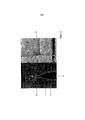
Фиг. 4 показывает поперечное сечение и вид сверху устройства с переходными отверстиями в подложке на стадиях производства фиг. 3b или фиг. 3c.FIG. 4 shows a cross section and a top view of a device with vias in a substrate in the manufacturing steps of FIG. 3b or FIG. 3c.
ПОДРОБНОЕ ОПИСАНИЕ ИЗОБРЕТЕНИЯDETAILED DESCRIPTION OF THE INVENTION
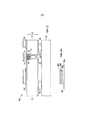
Каждая из фиг. 1a-c описывает поперечное сечение устройства с переходными отверстиями в подложке согласно первому варианту осуществления на различных стадиях производства. Фиг. 1c описывает законченное устройство 10 с переходными отверстиями в подложке согласно данному варианту осуществления. Устройство 10 с переходными отверстиями в подложке содержит подложку 12, сделанную из материала подложки и имеющую первую поверхность 12а подложки и вторую поверхность 12b подложки, противоположную первой поверхности 12а подложки. Устройство 10 с переходными отверстиями в подложке также содержит множество соседних первых канавок 14, обеспеченных проводящим материалом и проходящих с первой поверхности 12а подложки внутрь подложки 12, так что между первыми канавками 14 формируется множество спейсеров 16 из материала подложки. Устройство 10 с переходными отверстиями в подложке также содержит вторую канавку 18, обеспеченную проводящим материалом и проходящую со второй поверхности подложки внутрь подложки 12. Вторая канавка 18 (обеспеченная проводящим материалом) соединена с первыми канавками 14 (обеспеченными проводящим материалом). Посредством первых канавок 14 и второй канавки 18 формируется переходное отверстие сквозь всю подложку. Устройство с переходными отверстиями в подложке 10 также содержит проводящий слой 20, выполненный из проводящего материала и сформированный на стороне первой поверхности 12а подложки, проводящий материал заполняет первые канавки 14, так что первый проводящий слой 20 имеет по существу планарную, в особенности непористую и/или без выемок и предпочтительно закрытую поверхность.Each of FIG. 1a-c describes a cross-section of a device with vias in a substrate according to a first embodiment at various stages of production. FIG. 1c describes a
Материал подложки может быть электрически проводящим или полупроводящим материалом. В этом случае проводящий слой и электрически проводящий или полупроводящий материал подложки не контактируют напрямую, а электрически изолированы друг от друга, например, изолирующим слоем (не показан). Таким образом, подложка 12 может дополнительно содержать слой электрически изолирующей поверхности, например, обеспеченный посредством оксидирования. В другом случае материал подложки может быть электрически изолирующим материалом. В этом случае проводящий слой может быть напрямую нанесен на электрически изолирующий материал подложки.The substrate material may be an electrically conductive or semi-conductive material. In this case, the conductive layer and the electrically conductive or semiconducting substrate material do not contact directly, but are electrically isolated from each other, for example, by an insulating layer (not shown). Thus, the
Как показано на фиг. 1с, устройство с переходными отверстиями в подложке может дополнительно содержать второй проводящий слой 22, выполненный из проводящего материала и сформированный на второй поверхности 12b подложки. Второй проводящий слой 22 формируется на по меньшей мере части второй поверхности 12b подложки, окружающей вторую канавку 18. Между первым проводящим слоем 20 и вторым проводящим слоем 22 обеспечивается электрическое соединение. На поверхностях второй канавки 18 обеспечивается проводящий материал, так что первый проводящий слой 20 и второй проводящий слой 22 становятся электрически соединены. Предпочтительно первый проводящий слой 20 и второй проводящий слой 22 создаются из одного и того же проводящего материала (например, наносимого на одной и той же стадии производства), в частности. образуя общий слой, состоящий из одного и того же проводящего материала, как можно увидеть на фиг. 1с. В этом примере на той же самой стадии производства проводящий материал наносится на первую поверхность 12а подложки (таким образом формируя первый проводящий слой 20), первые канавки 14, на поверхности второй канавки 18 и вторую поверхность 12b подложки (таким образом формируя второй проводящий слой 22). Другими словами, проводящий материал наносится таким образом, что между первой поверхностью 12а подложки (или первым проводящим слоем 20) и второй поверхностью подложки 12b (или вторым проводящим слоем 22) обеспечивается электрическое соединение.As shown in FIG. 1c, the device with vias in the substrate may further comprise a second
Вторая канавка 18 имеет ширину w18, перекрывающую значительную часть первых канавок 14 и спейсеров 16 (или все канавки и спейсеры, за исключением крайних первых канавок). Здесь будет указано, что данный вариант осуществления обеспечивает предпочтительную ситуацию, при которой задняя (вторая) канавка 18 идеально выровнена с передними (первыми) канавками 14. Другие варианты осуществления, однако, все еще работают, если задняя канавка 18 не идеально выровнена до тех пор, пока есть электрическое соединение, и сопротивление достаточно низкое.The
Ширина w14 каждой из первых канавок 14 может, например, находиться в диапазоне между 0,5 мкм и 5 мкм. Поочередно или в сумме ширина w16 каждого спейсера 16 может, например, находиться в диапазоне между 0,5 мкм и 5 мкм. Глубина l16 каждой первой канавки 14 может быть меньше 100 мкм, в частности меньше 40 мкм. Поочередно или в сумме глубина l16 каждого спейсера 16 может быть меньше 100 мкм, в частности меньше 40 мкм. Отношение размеров первых канавок 14 и/или вторых канавок 16 может быть между 10 и 30, в частности около 20.The width w 14 of each of the
Только как пример ширина каждой из первых канавок 14 может быть около 1,5 мкм и/или ширина (оставшихся) спейсеров 16 может быть около 1 мкм, но этим не ограничена. Снова, только как пример глубина каждой из первых канавок может быть примерно от 30 до 40 мкм, но этим не ограничена. Только как пример, ширина второй канавки 18 (или переходного отверстия) может быть не меньше 20 мкм, согласно толщине подложки около 400 мкм и максимальному коэффициенту травления 20, но этим не ограничена. Только как пример, первый проводящий слой 20 и/или второй проводящий слой 22 могут иметь толщину примерно от 1 мкм до 2 мкм, но не ограничены ей. Будет подразумеваться, что возможны любые другие подходящие размеры. Just as an example, the width of each of the
Например, форма поперечного сечения каждой из первых канавок 14 может быть округлой и/или первые канавки 14 могут быть размещены в концентрической конфигурации (не показано), чтобы уменьшить давление.For example, the cross-sectional shape of each of the
Только как пример, подложка 12 может быть выполнена из кремния, но этим не ограничена. Также, только как пример, проводящий материал может быть поликремнием, но этим не ограничен. Осаждение поликремния в высокой степени однородно и может полностью запечатать узкие первые канавки 14.Just as an example, the
Сейчас способ производства устройства 10 с переходными отверстиями в подложке будет объяснен, ссылаясь на фиг. 1а-с. Данный способ начинается с обеспечения подложки 12, выполненной из материала подложки и имеющей первую поверхность 12а подложки и вторую поверхность 12b подложки, противоположную первой поверхности 12а подложки (см. фиг. 1а). Затем множество соседних первых канавок 14 вытравливается с первой поверхности 12а подложки внутрь подложки 12, так что множество спейсеров 16 из материала подложки формируется между первыми канавками 14 (см. фиг. 1a). Впоследствии вторая канавка 18 вытравливается со второй поверхности 12b подложки внутрь подложки 12, причем вторая канавка 18 соединена с первыми канавками 14 (см. фиг. 1b). Now, the manufacturing method of the
Затем на стороне первой поверхности 12a подложки (или на первую поверхность подложки 12а) обеспечивается (первый) проводящий слой 20, выполненный из проводящего материала, проводящий материал заполняет первые канавки 14, так что первый проводящий слой 20 имеет по существу планарную и закрытую поверхность. В некоторых случаях на второй поверхности 12b подложки может быть обеспечен второй проводящий слой 22, выполненный из проводящего материала. В частности, первый проводящий слой 20 и второй проводящий слой 22 могут быть нанесены на одной и той же стадии производства (например, формирование общего слоя, выполненного из того же материала), как можно увидеть на фиг. 1с.Then, on the side of the
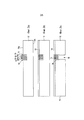
Фиг. 2 описывает сборку 100 емкостного ультразвукового преобразователя, подвергнутого микрообработке (CMUT), согласно первому варианту осуществления. Сборка 100 CMUT содержит устройство 10 с переходными отверстиями в подложке. Сборка 100 CMUT также содержит по меньшей мере одну ячейку 30 CMUT, электрически соединенную с первым проводящим слоем 20. Сборка 100 CMUT может, в частности, содержать множество ячеек 30 CMUT, как обозначено на фиг. 2 первой и второй ячейками 30 CMUT. Будет подразумеваться, что может быть использовано любое подходящее число ячеек CMUT. Ячейки CMUT могут сформировать ультразвуковую матрицу CMUT, в частности линейную (1-D) матрицу или двумерную (2-D) матрицу. Сборка CMUT может, например, быть использована для 2-D ультразвуковой визуализации и 3-D ультразвуковой визуализации.FIG. 2 describes an
Устройство 10 с переходными отверстиями в подложке, описанное на фиг. 2, может быть устройством с переходными отверстиями в подложке варианта осуществления по фиг. 1с. В отличие от устройства с переходными отверстиями в подложке варианта осуществления по фиг. 1с устройство 10 с переходными отверстиями в подложке фиг.2 также содержит электрическое соединение 39 (например, столбиковые выводы из припоя) между вторым проводящим слоем 22 и ASIC 40. ASIC 40 затем используется для обеспечения электрических сигналов по меньшей мере к одной ячейке 30 CMUT.The
Фиг. 2а описывает поперечное сечение ячейки CMUT. Ячейка 30 CMUT содержит нижний электрод 30а, полость 30b, мембрану 30с, размещенную на полости 30b, и верхний электрод 30d. Будет подразумеваться, что ячейка CMUT по фиг. 2а только примерная основная ячейка CMUT. Ячейка CMUT сборки 100 CMUT согласно настоящему изобретению может содержать любой подходящий тип ячейки CMUT.FIG. 2a describes a cross section of a CMUT cell. The
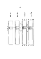
Каждая из фиг. 3a-g описывает поперечное сечение устройства с переходными отверстиями в подложке согласно второму варианту осуществления на различных стадиях производства. Устройство с переходными отверстиями в подложке второго варианта осуществления может, например, быть использовано в сборке CMUT первого варианта осуществления по фиг. 2, описанного выше.Each of FIG. 3a-g describes a cross-section of a device with vias in a substrate according to a second embodiment at various stages of production. The device with vias in the substrate of the second embodiment may, for example, be used in the CMUT assembly of the first embodiment of FIG. 2 described above.
Как уже объяснялось, ссылаясь на фиг. 1а-с, данный способ начинается с обеспечения подложки 12, выполненной из материала подложки и имеющей первую поверхность 12а подложки и вторую поверхность 12b подложки, противоположную первой поверхности 12а подложки (фиг. 3а). Например, подложка 12 может быть пустой кремниевой подложкой. Предпочтительно подложка 12 настолько тонка, насколько это возможно, чтобы облегчить вытравливание переходных отверстий в подложке, и в то же время достаточно толстой, чтобы обеспечить достаточную механическую поддержку и/или манипулирование.As already explained, referring to FIG. 1a-c, this method begins by providing a
Только как пример, для подложки, имеющей диаметр 150 мм, толщина подложки 400 мкм - хороший выбор.Just as an example, for a substrate having a diameter of 150 mm, a substrate thickness of 400 μm is a good choice.
Затем, как показано на фиг. 3а, множество соседних первых канавок 14 вытравливаются с первой (лицевой) поверхности 12а подложки внутрь подложки 12, так что между первыми канавками 14 формируется множество спейсеров 16 из материала подложки.Then, as shown in FIG. 3a, a plurality of adjacent
Например, это может быть произведено, используя реактивное ионное травление (RIE).For example, this can be done using reactive ion etching (RIE).
Впоследствии, как можно увидеть на фиг. 3b, слой 13, препятствующий травлению, наносится на первую поверхность подложки после вытравливания первых канавок 14. Например, слой 13, препятствующий травлению, может быть выполнен из оксида и/или может быть нанесен, используя PECVD. Потому что оксид PECVD осаждается со слабой конформностью, первые канавки будут автоматически запечатаны после того как осаждены несколько микрон оксида. Только как пример толщина слоя, препятствующего травлению, может быть примерно между 4 мкм и 6 мкм.Subsequently, as can be seen in FIG. 3b, the
Затем, как показано на фиг. 4с, вторая канавка 18 (или переходное отверстие) вытравливается из второй (задней) поверхности 12b подложки внутрь подложки 12, вторая канавка 18 соединена с первыми канавками 14. Вторая канавка 18 имеет контакт или оканчивается в области, в которой расположены первые канавки 14. Фиг. 4 описывает поперечное сечение и вид сверху устройства с переходными отверстиями в подложке на стадии производства на фиг. 3b или фиг. 3с.Then, as shown in FIG. 4c, the second groove 18 (or transition hole) is etched from the second (back)
Ссылаясь на фиг. 3d, после вытравливания второй канавки 18 слой 13, препятствующий травлению, удаляется.Referring to FIG. 3d, after etching the
Затем, как можно увидеть на фиг. 3e, подложка 12 обеспечивается слоем 15 электрически изолирующей поверхности (например, оксидированием, в особенности высокотемпературным оксидированием). Таким образом, боковые поверхности второй канавки 18, первых канавок 14 и спейсеров 16 обеспечиваются слоем 15 изолирующей поверхности.Then, as can be seen in FIG. 3e, the
Впоследствии, как описано на фиг. 3f, проводящий слой 20, выполненный из проводящего материала, обеспечивается на стороне первой поверхности 12а подложки, проводящий материал заполняет первые канавки 14, так что первый проводящий слой 20 имеет по существу планарную и закрытую поверхность. На том же этапе обработки проводящий материал также наносится на вторую поверхность 12b подложки (таким образом формируя второй проводящий слой 22) и на поверхности вторых канавок 18. Таким образом, первый проводящий слой 20 и второй проводящий слой 22 электрически соединены.Subsequently, as described in FIG. 3f, a
Затем, как можно увидеть на фиг. 3g, на первой (передней) поверхности подложки структурируется первый проводящий слой 20. Структурирование второго проводящего слоя 22 на вторую (заднюю) поверхность подложки может быть произведено на поздней стадии. Например, в некоторых сборках CMUT (здесь не показано) первый проводящий слой 14 может быть напрямую использован как нижний электрод ячейки CMUT. На этой стадии производство (высокотемпературного) устройства с переходными отверстиями в подложке практически завершено. Then, as can be seen in FIG. 3g, a first
Затем обработка ячейки 30 CMUT может начинаться. Например, первый нижний электрод 30а закрепляется на устройстве 10 с переходными отверстиями в подложке (в частности, на первом проводящем слое 27 или на дополнительном слое, таком как оксидный слой). Затем обеспечивается оставшаяся часть ячейки 30 CMUT, в частности полость 30b, мембрана 30с, размещенная на полости 30b, и верхний электрод 30d, как объясняется согласно фиг. 2а.Then, processing of the
В конце может быть обеспечено электрическое соединение 39 между вторым проводящим слоем 22 и ASIC 40. Сборка CMUT может затем быть монтирована на ASIC способом перевернутого кристалла (например, с помощью столбикового вывода из припоя) (см. фиг. 2).At the end, an
Чтобы привести одно конкретное применение, 3D ультразвуковая визуализация с электронным сканированием требует электронику формирования луча, вплотную интегрированную с акустическими элементами. В гибридной сборке или устройстве CMUT (емкостной ультразвуковой преобразователь, подвергнутый микрообработке) специализированное устройство с переходными отверстиями, содержащее матрицу ячеек преобразователей CMUT или элементов на нем (все вместе называемое кремниевой ИС), монтируется способом перевернутого кристалла наверху отдельного чипа ASIC, который содержит всю электронику, чтобы управлять каждой отдельной ячейкой преобразователя или элементом (или пикселом). Этот подход возможен только при подходящей технологии переходных отверстий в подложке, которая соединяет ячейку CMUT или элемент на лицевой стороне устройства с переходными отверстиями в подложке с ASIC на тыльной стороне устройства с переходными отверстиями в подложке. Технология переходных отверстий в подложке обычно очень сложна, потому что нормально они выполняются после обработки активного устройства (т. е. с интегрированной электроникой) и, следовательно, подвергаются серьезным ограничениям обработки, особенно в отношении допустимого температурного запаса. В этом особом случае устройства «пассивного CMUT» (т.е. без встроенной электроники), однако, возможно сначала обработать переходные отверстия в подложке или устройство с переходными отверстиями в подложке, а затем изготовить ячейки CMUT. Таким образом, изготовление устройства с переходными отверстиями в подложке может быть значительно упрощено. В этом описании изобретения обсуждается особенно привлекательная последовательность технологических операций, которая выдает в результате планарную верхнюю поверхность. Конкретное применение усовершенствованного устройства CMUT представлено.To cite one specific application, 3D ultrasound imaging with electronic scanning requires beamforming electronics that are closely integrated with acoustic elements. In a hybrid assembly or CMUT device (micro-processed capacitive ultrasonic transducer), a specialized vias device containing a matrix of CMUT transducer cells or elements on it (collectively referred to as a silicon IC) is mounted by the inverted crystal method on top of a separate ASIC chip that contains all the electronics to control each individual transducer cell or element (or pixel). This approach is only possible with a suitable vias in the substrate, which connects the CMUT cell or element on the front of the device with vias in the substrate with an ASIC on the back of the device with vias in the substrate. The technology of vias in a substrate is usually very complicated, because they are normally performed after processing an active device (i.e., with integrated electronics) and, therefore, are subject to severe processing limitations, especially with regard to the allowable temperature margin. In this special case of a “passive CMUT” device (ie, without integrated electronics), however, it is possible to first process the vias in the substrate or the vias with vias in the substrate, and then fabricate the CMUT cells. Thus, the manufacture of a device with vias in the substrate can be greatly simplified. This description of the invention discusses a particularly attractive process flow that results in a planar upper surface. The specific application of the advanced CMUT device is presented.
Возможно в таком случае начать с изготовления переходных отверстий в подложке, а затем изготавливать устройства CMUT. Кроме того, требования для сопротивления переходных отверстий в подложке не такие строгие, как, например, для устройств стековой памяти. Подводя итог изложенному, это делает возможным использование высокотемпературных техник осаждения (термальное оксидирование и LPCVD) для изоляции и заполнения переходных отверстий. Это значительно упрощает их изготовление.It is possible in this case to start with the manufacture of vias in the substrate, and then make CMUT devices. In addition, the requirements for the resistance of vias in the substrate are not as stringent as, for example, for stack memory devices. To summarize, this makes it possible to use high-temperature deposition techniques (thermal oxidation and LPCVD) to isolate and fill vias. This greatly simplifies their manufacture.
Устройство с переходными отверстиями в подложке настоящего изобретения может, в частности, быть использовано для сборки емкостного преобразователя, подвергнутого микрообработке (CMUT), как описано выше. Однако будет подразумеваться, что устройство с переходными отверстиями в подложке настоящего изобретения может также быть использовано для другого устройства или сборки, таких как, например, любой датчик или устройство MEMS. Например, устройство с переходными отверстиями в подложке настоящего изобретения может также быть использовано для тонкопленочного или подвергнутого микрообработке датчика, катетера, проволочного проводника катетера с измерительным датчиком и/или визуализацией и интегрированной электроникой, устройства интракардиальной эхографии (ICE), устройства внутрисосудистого ультразвукового исследования (IVUS), визуализации и датчика измерений внутри тела, хирургического или терапевтического устройства с системой визуализации (IGIT).The through-hole device of the substrate of the present invention can, in particular, be used to assemble a microprocessed capacitive transducer (CMUT) as described above. However, it will be understood that the device with vias in the substrate of the present invention can also be used for another device or assembly, such as, for example, any sensor or MEMS device. For example, a device with vias in the substrate of the present invention can also be used for a thin-film or micro-processed sensor, catheter, catheter guidewire with a measuring sensor and / or imaging and integrated electronics, intracardial ultrasound imaging (ICE) device, intravascular ultrasound (IVUS) device ), a visualization and measurement sensor inside the body, a surgical or therapeutic device with an imaging system (IGIT).
Несмотря на то, что данное изобретение было проиллюстрировано и детально описано на чертежах и предшествующем описании, такие иллюстрация и описание должны рассматриваться как иллюстративные и примерные и неограничительные; изобретение не ограничено раскрытыми примерами реализации.Although the invention has been illustrated and described in detail in the drawings and the preceding description, such illustration and description should be considered as illustrative and exemplary and not restrictive; the invention is not limited to the disclosed implementation examples.
Другие вариации раскрытых примеров реализации могут быть поняты и воспроизведены специалистами в данной области в практической реализации изобретения, описанного в формуле изобретения, от изучения чертежей, раскрытия сущности и приложенной формулы изобретения.Other variations of the disclosed exemplary embodiments may be understood and reproduced by those skilled in the art in the practice of the invention described in the claims, from the study of the drawings, the disclosure, and the appended claims.
В формуле изобретения слово «содержащий» не исключает другие элементы или этапы, а единственное число не исключает множественность. Один элемент или другой компонент могут выполнить функции нескольких пунктов, перечисленных в формуле изобретения. Простой факт, что определенные меры перечислены во взаимно различных зависимых пунктах формулы изобретения, не указывает на то, что комбинация этих мер не может быть использована с выгодой.In the claims, the word “comprising” does not exclude other elements or steps, and the singular does not exclude plurality. One element or another component can fulfill the functions of several points listed in the claims. The simple fact that certain measures are listed in mutually different dependent claims does not indicate that a combination of these measures cannot be used to advantage.
Любые условные обозначения в формуле изобретения не следует интерпретировать как ограничивающие объем.Any conventions in the claims should not be interpreted as limiting the scope.
Claims (13)
- подложку (12), выполненную из материала подложки и имеющую первую поверхность (12а) подложки и вторую поверхность (12b) подложки, противоположную первой поверхности (12а) подложки,
- множество соседних первых канавок (14), обеспеченных проводящим материалом и проходящих с первой поверхности (12а) подложки внутрь подложки (12), так что между первыми канавками (14) формируется множество спейсеров (16) из материала подложки,
- вторую канавку (18), обеспеченную проводящим материалом и проходящую со второй поверхности (12b) подложки внутрь материала подложки (12), причем вторая канавка (18) соединена с первыми канавками (14),
- проводящий слой (20), выполненный из проводящего материала и сформированный на стороне первой поверхности (12а) подложки, причем проводящий материал заполняет первые канавки (14), так что первый проводящий слой (20) имеет по существу планарную и закрытую поверхность, покрывающую заполненные первые канавки и формирующую электрическое соединение между заполненными канавками.1. The device (10) with vias in the substrate, containing:
- a substrate (12) made of a substrate material and having a first substrate surface (12a) and a second substrate surface (12b) opposite the first substrate surface (12a),
- a plurality of adjacent first grooves (14) provided with a conductive material and extending from the first surface (12a) of the substrate into the substrate (12), so that many spacers (16) are formed between the first grooves (14) from the substrate material,
- a second groove (18) provided with a conductive material and extending from the second substrate surface (12b) into the substrate material (12), the second groove (18) being connected to the first grooves (14),
a conductive layer (20) made of conductive material and formed on the side of the first substrate surface (12a), the conductive material filling the first grooves (14), so that the first conductive layer (20) has a substantially planar and closed surface covering the filled first grooves and forming an electrical connection between the filled grooves.
- обеспечение подложки (12), выполненной из материала подложки и имеющей первую поверхность (12а) подложки и вторую поверхность (12b) подложки, противоположную первой поверхности (12а) подложки,
- вытравливание множества соседних первых канавок (14) с первой поверхности (12а) подложки внутрь материала подложки (12), так что между первыми канавками (14) формируется множество спейсеров (16) из материала подложки,
- вытравливание второй канавки (18) со второй поверхности (12b) подложки внутрь подложки (12), причем вторая канавка (18) соединена с первыми канавками (14), и
- обеспечение проводящего слоя (20), выполненного из проводящего материала на стороне первой поверхности (12а) подложки, причем проводящий материал заполняет первые канавки (14), так что первый проводящий слой (20) имеет по существу планарную и закрытую поверхность, покрывающую заполненные первые канавки и формирующую электрическое соединение между заполненными первыми канавками. 13. A method of manufacturing a device (10) with vias in a substrate, the method comprising:
- providing a substrate (12) made of a substrate material and having a first substrate surface (12a) and a second substrate surface (12b) opposite the first substrate surface (12a),
etching the plurality of adjacent first first grooves (14) from the first substrate surface (12a) into the substrate material (12), such that a plurality of spacers (16) are formed between the first grooves (14) from the substrate material,
etching the second groove (18) from the second surface (12b) of the substrate into the substrate (12), the second groove (18) being connected to the first grooves (14), and
- providing a conductive layer (20) made of conductive material on the side of the first substrate surface (12a), the conductive material filling the first grooves (14), so that the first conductive layer (20) has a substantially planar and closed surface covering the filled first grooves and forming an electrical connection between the filled first grooves.
Applications Claiming Priority (3)
| Application Number | Priority Date | Filing Date | Title |
|---|---|---|---|
| US201161547942P | 2011-10-17 | 2011-10-17 | |
| US61/547,942 | 2011-10-17 | ||
| PCT/IB2012/055547 WO2013057642A1 (en) | 2011-10-17 | 2012-10-12 | Through-wafer via device and method of manufacturing the same |
Publications (2)
| Publication Number | Publication Date |
|---|---|
| RU2014119923A RU2014119923A (en) | 2015-11-27 |
| RU2603435C2 true RU2603435C2 (en) | 2016-11-27 |
Family
ID=47428773
Family Applications (1)
| Application Number | Title | Priority Date | Filing Date |
|---|---|---|---|
| RU2014119923/28A RU2603435C2 (en) | 2011-10-17 | 2012-10-12 | Through-wafer via device and method of manufacturing the same |
Country Status (6)
| Country | Link |
|---|---|
| US (1) | US9230908B2 (en) |
| EP (1) | EP2745315A1 (en) |
| CN (1) | CN103875068B (en) |
| IN (1) | IN2014CN02550A (en) |
| RU (1) | RU2603435C2 (en) |
| WO (1) | WO2013057642A1 (en) |
Families Citing this family (5)
| Publication number | Priority date | Publication date | Assignee | Title |
|---|---|---|---|---|
| CN104023860B (en) | 2011-12-20 | 2016-06-15 | 皇家飞利浦有限公司 | Ultrasonic transducer equipment and the method manufacturing described ultrasonic transducer equipment |
| EP3126065B1 (en) | 2014-03-31 | 2021-05-19 | Koninklijke Philips N.V. | Ic die, ultrasound probe, ultrasonic diagnostic system and method |
| CN107078061B (en) * | 2015-03-16 | 2020-07-10 | 富士电机株式会社 | Method for manufacturing semiconductor device |
| US11097942B2 (en) * | 2016-10-26 | 2021-08-24 | Analog Devices, Inc. | Through silicon via (TSV) formation in integrated circuits |
| WO2019213448A1 (en) * | 2018-05-03 | 2019-11-07 | Butterfly Network, Inc. | Vertical packaging for ultrasound-on-a-chip and related methods |
Citations (2)
| Publication number | Priority date | Publication date | Assignee | Title |
|---|---|---|---|---|
| US6430109B1 (en) * | 1999-09-30 | 2002-08-06 | The Board Of Trustees Of The Leland Stanford Junior University | Array of capacitive micromachined ultrasonic transducer elements with through wafer via connections |
| RU2419179C2 (en) * | 2006-12-20 | 2011-05-20 | Интел Корпорейшн | Integrated circuit device and method of making said device |
Family Cites Families (17)
| Publication number | Priority date | Publication date | Assignee | Title |
|---|---|---|---|---|
| US5381385A (en) | 1993-08-04 | 1995-01-10 | Hewlett-Packard Company | Electrical interconnect for multilayer transducer elements of a two-dimensional transducer array |
| US5619476A (en) * | 1994-10-21 | 1997-04-08 | The Board Of Trustees Of The Leland Stanford Jr. Univ. | Electrostatic ultrasonic transducer |
| US6716737B2 (en) * | 2002-07-29 | 2004-04-06 | Hewlett-Packard Development Company, L.P. | Method of forming a through-substrate interconnect |
| US20040104454A1 (en) * | 2002-10-10 | 2004-06-03 | Rohm Co., Ltd. | Semiconductor device and method of producing the same |
| US6836020B2 (en) | 2003-01-22 | 2004-12-28 | The Board Of Trustees Of The Leland Stanford Junior University | Electrical through wafer interconnects |
| US7257051B2 (en) * | 2003-03-06 | 2007-08-14 | General Electric Company | Integrated interface electronics for reconfigurable sensor array |
| JP2005032769A (en) * | 2003-07-07 | 2005-02-03 | Seiko Epson Corp | Method of forming multilayer wiring, method of manufacturing wiring board, and method of manufacturing device |
| WO2005088699A1 (en) * | 2004-03-10 | 2005-09-22 | Koninklijke Philips Electronics N.V. | Method of manufacturing an electronic device and a resulting device |
| EP1779784B1 (en) | 2004-06-07 | 2015-10-14 | Olympus Corporation | Electrostatic capacity type ultrasonic transducer |
| WO2006123298A2 (en) | 2005-05-18 | 2006-11-23 | Kolo Technologies, Inc. | Through-wafer interconnection |
| US7622848B2 (en) | 2006-01-06 | 2009-11-24 | General Electric Company | Transducer assembly with z-axis interconnect |
| CN101479845A (en) | 2006-06-26 | 2009-07-08 | 皇家飞利浦电子股份有限公司 | Flip-chip interconnection with a small passivation layer opening |
| JP5175853B2 (en) | 2006-09-25 | 2013-04-03 | コーニンクレッカ フィリップス エレクトロニクス エヌ ヴィ | Flip chip interconnect through chip vias |
| KR101335200B1 (en) * | 2006-11-03 | 2013-11-29 | 리써치 트라이앵글 인스티튜트 | Enhanced ultrasound imaging probes using flexure mode piezoelectric transducers |
| US7843022B2 (en) | 2007-10-18 | 2010-11-30 | The Board Of Trustees Of The Leland Stanford Junior University | High-temperature electrostatic transducers and fabrication method |
| US7781238B2 (en) | 2007-12-06 | 2010-08-24 | Robert Gideon Wodnicki | Methods of making and using integrated and testable sensor array |
| US8062975B2 (en) | 2009-04-16 | 2011-11-22 | Freescale Semiconductor, Inc. | Through substrate vias |
-
2012
- 2012-10-12 US US14/346,824 patent/US9230908B2/en active Active
- 2012-10-12 IN IN2550CHN2014 patent/IN2014CN02550A/en unknown
- 2012-10-12 CN CN201280050826.8A patent/CN103875068B/en active Active
- 2012-10-12 WO PCT/IB2012/055547 patent/WO2013057642A1/en active Application Filing
- 2012-10-12 RU RU2014119923/28A patent/RU2603435C2/en active
- 2012-10-12 EP EP12805761.9A patent/EP2745315A1/en not_active Withdrawn
Patent Citations (2)
| Publication number | Priority date | Publication date | Assignee | Title |
|---|---|---|---|---|
| US6430109B1 (en) * | 1999-09-30 | 2002-08-06 | The Board Of Trustees Of The Leland Stanford Junior University | Array of capacitive micromachined ultrasonic transducer elements with through wafer via connections |
| RU2419179C2 (en) * | 2006-12-20 | 2011-05-20 | Интел Корпорейшн | Integrated circuit device and method of making said device |
Also Published As
| Publication number | Publication date |
|---|---|
| CN103875068B (en) | 2018-07-10 |
| RU2014119923A (en) | 2015-11-27 |
| WO2013057642A1 (en) | 2013-04-25 |
| CN103875068A (en) | 2014-06-18 |
| US9230908B2 (en) | 2016-01-05 |
| IN2014CN02550A (en) | 2015-08-07 |
| EP2745315A1 (en) | 2014-06-25 |
| US20140293751A1 (en) | 2014-10-02 |
Similar Documents
| Publication | Publication Date | Title |
|---|---|---|
| US10835922B2 (en) | Ultrasound transducer device and method of manufacturing the same | |
| US8324006B1 (en) | Method of forming a capacitive micromachined ultrasonic transducer (CMUT) | |
| US9224648B2 (en) | Through-wafer interconnection | |
| KR101761818B1 (en) | Electro-acoustic trasnducer and method of manufacturing the same | |
| RU2603435C2 (en) | Through-wafer via device and method of manufacturing the same | |
| US20220048071A1 (en) | Ic die, probe and ultrasound system | |
| US9596528B2 (en) | Capacitive micromachined ultrasonic transducer and method of fabricating the same | |
| US20100255623A1 (en) | Packaging and Connecting Electrostatic Transducer Arrays | |
| US9475092B2 (en) | Electro-acoustic transducer and method of manufacturing the same | |
| EP2988883A1 (en) | Capacitive micromachined ultrasonic transducer (cmut) with through-substrate via (tsv) substrate plug | |
| US10898925B2 (en) | Ultrasound transducer assembly and method for manufacturing an ultrasound transducer assembly | |
| KR101851569B1 (en) | Ultrasonic transducer and method of manufacturig the same | |
| JP4835082B2 (en) | Semiconductor device and manufacturing method thereof | |
| KR101851568B1 (en) | Ultrasonic transducer and method of manufacturig the same | |
| CN110773408A (en) | Capacitive micro-nano ultrasonic transducer and preparation method thereof | |
| WO2013089648A1 (en) | Capacitive micromachined ultrasonic transducer arrangement and method of fabricating the same |