RU2565331C2 - Method of investigation spatial distribution of receptivity of characteristics of photoelectric converters in solar panels to optical radiation - Google Patents
Method of investigation spatial distribution of receptivity of characteristics of photoelectric converters in solar panels to optical radiation Download PDFInfo
- Publication number
- RU2565331C2 RU2565331C2 RU2013145259/28A RU2013145259A RU2565331C2 RU 2565331 C2 RU2565331 C2 RU 2565331C2 RU 2013145259/28 A RU2013145259/28 A RU 2013145259/28A RU 2013145259 A RU2013145259 A RU 2013145259A RU 2565331 C2 RU2565331 C2 RU 2565331C2
- Authority
- RU
- Russia
- Prior art keywords
- laser
- radiation
- scanning
- parameters
- solar
- Prior art date
Links
Images
Classifications
-
- Y—GENERAL TAGGING OF NEW TECHNOLOGICAL DEVELOPMENTS; GENERAL TAGGING OF CROSS-SECTIONAL TECHNOLOGIES SPANNING OVER SEVERAL SECTIONS OF THE IPC; TECHNICAL SUBJECTS COVERED BY FORMER USPC CROSS-REFERENCE ART COLLECTIONS [XRACs] AND DIGESTS
- Y02—TECHNOLOGIES OR APPLICATIONS FOR MITIGATION OR ADAPTATION AGAINST CLIMATE CHANGE
- Y02E—REDUCTION OF GREENHOUSE GAS [GHG] EMISSIONS, RELATED TO ENERGY GENERATION, TRANSMISSION OR DISTRIBUTION
- Y02E10/00—Energy generation through renewable energy sources
- Y02E10/50—Photovoltaic [PV] energy
-
- Y—GENERAL TAGGING OF NEW TECHNOLOGICAL DEVELOPMENTS; GENERAL TAGGING OF CROSS-SECTIONAL TECHNOLOGIES SPANNING OVER SEVERAL SECTIONS OF THE IPC; TECHNICAL SUBJECTS COVERED BY FORMER USPC CROSS-REFERENCE ART COLLECTIONS [XRACs] AND DIGESTS
- Y02—TECHNOLOGIES OR APPLICATIONS FOR MITIGATION OR ADAPTATION AGAINST CLIMATE CHANGE
- Y02P—CLIMATE CHANGE MITIGATION TECHNOLOGIES IN THE PRODUCTION OR PROCESSING OF GOODS
- Y02P70/00—Climate change mitigation technologies in the production process for final industrial or consumer products
- Y02P70/50—Manufacturing or production processes characterised by the final manufactured product
Landscapes
- Photovoltaic Devices (AREA)
- Testing Of Individual Semiconductor Devices (AREA)
Abstract
Description
Изобретение относится к классу устройств для визуального представления измеряемых электрических переменных величин в цифровом виде и предназначено для исследования пространственного распределения характеристик восприимчивости фотоэлектрических преобразователей (ФЭП) в составе солнечных батарей к оптическому излучению. Исследование производится путем сканирования поверхности исследуемого объекта лазерным лучом с помощью гальваносканеров с одновременной записью координат сканирования и напряжения, пропорционального величине фотоотклика в данной точке исследуемого объекта. Устройство может быть использовано для контроля качества готовых изделий на предприятиях полупроводниковой промышленности.The invention relates to a class of devices for the visual representation of measured electrical variables in digital form and is intended to study the spatial distribution of the susceptibility characteristics of photovoltaic converters (PECs) in solar cells to optical radiation. The study is performed by scanning the surface of the test object with a laser beam using galvanoscanners with simultaneous recording of the scan coordinates and voltage proportional to the magnitude of the photoresponse at a given point of the test object. The device can be used to control the quality of finished products at the enterprises of the semiconductor industry.
Из уровня техники известен один из вариантов реализации оптической системы контроля для обнаружения трещин в кремниевой подложке или в эпитаксиальных слоях солнечного элемента (патент CA 2118743). В качестве лазера (коллимированного луча света) используется гелий-неоновый лазер. В нем видеокамера с макрообъективом расположена коллинеарно с лазером. Лазер используется для наведения видеокамеры. Видеокамера чувствительна к ближней инфракрасной области частот. Тестируемая солнечная батарея расположена на пути распространения лазерного луча и в области зрения видеокамеры. Коллимированное излучение из источника, например кварцевой галогеновой лампы, обеспечивающей освещение от 0,9 до 1,2 мкм (ближний инфракрасный спектр), проецируется через длинноволновый фильтр, через который проходят только волны с длиной 1,0 мкм. Отфильтрованный коллимированный свет от источника света проецируется на поверхность белой бумажной панели. Солнечная батарея также освещается неколлимированным нефильтрованным ближним инфракрасным светом, направленным под другим углом от второй кварц-галогенной лампы.One embodiment of an optical inspection system for detecting cracks in a silicon substrate or in the epitaxial layers of a solar cell is known from the prior art (patent CA 2118743). A helium-neon laser is used as a laser (collimated light beam). In it, a video camera with a macro lens is located collinear with a laser. The laser is used to aim the camcorder. The camcorder is sensitive to near infrared frequencies. The tested solar battery is located in the path of the laser beam and in the field of view of the camera. Collimated radiation from a source, such as a quartz halogen lamp that provides illumination from 0.9 to 1.2 μm (near infrared spectrum), is projected through a long-wave filter through which only waves with a length of 1.0 μm pass. The filtered collimated light from the light source is projected onto the surface of a white paper panel. The solar panel is also illuminated by uncollimated unfiltered near-infrared light directed at a different angle from the second quartz-halogen lamp.
Лицевая сторона белой бумаги содержит включения размером порядка 1,0 микрона - того же порядка, что и длина волны, проходящей через фильтр. Эти неровности свет, отраженный от поверхности белой бумаги, делают диффузным. Белая бумага расположена таким образом, чтобы отраженный от нее диффузный свет падал на поверхность солнечной панели. Свет, отраженный от белой бумаги, не видимый невооруженным глазом, попадает на поверхность солнечной панели под множеством различных углов.The front side of the white paper contains inclusions of the order of 1.0 micron in size - the same order as the wavelength passing through the filter. These irregularities make light reflected from the surface of white paper diffuse. White paper is positioned so that diffuse light reflected from it hits the surface of the solar panel. Light reflected from white paper, not visible to the naked eye, hits the surface of the solar panel at many different angles.
Лучи света могут быть либо отражены одним из слоев ФЭП, либо пройти к следующему слою. Полное внутреннее отражение будет происходить только для определенных световых лучей от слоя между воздухом и антибликовым покрытием. Некоторые из лучей будут отражены обратно на белую бумагу, а другие будут отражены в направлении поля зрения камеры и объектива. Лучи, попадающие в поле зрения камеры, становятся изображением объекта, которое может быть просмотрено на контрольном мониторе, связанном с видеокамерой. Изображение, которое видно на контрольном мониторе, обусловлено лишь вкладом первого коллимированного кварцевого галогенного источника, свет которого прошел через фильтр. Второй источник света нефильтрованной неколлимированной кварц-галогенной лампы используется для освещения солнечной панели, когда необходимо проверить наличие трещин в защитном стекле или трещин в непокрытом еще защитным стеклом кремнии. Детектирование дефектов с помощью данного метода основано на разнице показателей преломления бездефектной поверхности подложки кремниевых ФЭП и треснувших участков, образующих затененные области на получаемом изображении.The rays of light can either be reflected by one of the layers of the photomultiplier, or pass to the next layer. Full internal reflection will occur only for certain light rays from the layer between the air and the anti-reflective coating. Some of the rays will be reflected back onto the white paper, while others will be reflected in the direction of the field of view of the camera and lens. The rays falling into the field of view of the camera become an image of an object that can be viewed on the control monitor associated with the video camera. The image that is visible on the control monitor is due only to the contribution of the first collimated quartz halogen source, the light of which passed through the filter. A second light source of unfiltered uncollimated quartz-halogen lamp is used to illuminate the solar panel when it is necessary to check for cracks in the protective glass or cracks in silicon that is not yet covered with protective glass. Defect detection using this method is based on the difference in the refractive indices of the defect-free surface of the silicon PEC substrate and the cracked areas forming shaded areas in the resulting image.
Из уровня техники известен метод обнаружения дефектов солнечных элементов (патент CN 101988904). Схема метода включает в себя расширитель лазерного луча перемещающий его по солнечной батарее и регулирующий размер лазерного пятна для того, чтобы оно могло покрыть весь солнечный элемент; контроллер, регулирующий длину волны лазерного луча, чтобы заставить солнечный элемент люминесцировать. Камера ориентируется по солнечной батарее, чтобы снимать ее электролюминесценцию. Снятые на камеру изображения загружаются на компьютер через линию передачи данных и затем анализируются компьютерной программой на предмет наличия дефектов в солнечной батарее. С помощью расширителя лазерного луча, через который непосредственно диффундирует излучение, испускаемое полупроводниковым лазером, оно попадает на всю поверхность солнечного элемента. Таким образом, солнечные элементы могут быть исследованы без перемещения, даже если они тестируются не в составе солнечной батареи. Контроллер управляет длиной волны излучения лазера, благодаря чему люминесценция солнечного элемента постоянно поддерживается в оптимальном состоянии и точность обнаружения дефектов увеличивается.The prior art method for detecting defects in solar cells (patent CN 101988904). The scheme of the method includes a laser beam expander moving it around the solar battery and adjusting the size of the laser spot so that it can cover the entire solar cell; a controller adjusting the wavelength of the laser beam to cause the solar cell to luminesce. The camera is guided by the solar battery to remove its electroluminescence. Images taken on a camera are downloaded to a computer via a data line and then analyzed by a computer program for defects in the solar battery. Using a laser beam expander through which the radiation emitted by a semiconductor laser directly diffuses, it enters the entire surface of the solar cell. Thus, solar cells can be investigated without moving, even if they are not tested in the solar panel. The controller controls the wavelength of the laser radiation, due to which the luminescence of the solar cell is constantly maintained in optimal condition and the accuracy of detection of defects increases.
Из уровня техники известно устройство контроля качества солнечных батарей (патент JP 2009122036). Устройство контроля качества солнечных элементов имеет ленточный транспортер, с помощью которого осуществляется перемещение подложки, на которой закреплена солнечная батарея. Фотокамера линейно перемещается, чтобы фотографировать подложку в каждой из множества позиций. Светоизлучающий элемент излучает через собирающую линзу, фокусирующую свет на подложку для фотографирования области с помощью фотокамеры. Цифровые фото поступают в секцию обработки изображений - компьютер обнаруживает выступы металла на электродах солнечной батареи на основе сфотографированных во множестве положений изображений подложки.The prior art device quality control solar panels (patent JP 2009122036). The quality control device of solar cells has a conveyor belt, with the help of which the substrate is moved, on which the solar battery is mounted. The camera moves linearly to photograph the substrate in each of a variety of positions. A light-emitting element emits through a collecting lens focusing the light on a substrate for photographing an area using a camera. Digital photos enter the image processing section - the computer detects the protrusions of the metal on the electrodes of the solar battery based on photographed in many positions of the substrate images.
Из уровня техники известен пример применения неразрушающего метода для поиска дефектов в фотодетекторах и ФЭП (патент US 4,287,473). Для сканирования с помощью света отдается предпочтение лазеру с низкой мощностью. В реализации может быть использован непрерывный He-Ne-лазер или другие эквивалентные источники света. В случае, если изучаемый ФЭП является кремниевым, желательно, чтобы длина волны лазера составляла 0,633 мкм. Зеркала M1 и M2 используются для вывода лазерного излучения для того, чтобы сделать лазер более компактным и прочным, но свет может быть направлен на ФЭП и другими эквивалентными средствами. Анализатор, расположенный на выходе из лазера, используется для управления интенсивностью излучения и добавляется к устройству при тестировании. Поскольку на выходе из лазера угол поляризационной плоскости может варьироваться (коэффициент пропускания изменяется от 0 до 1), используются зеркала V и H с электрическим приводом, чтобы обеспечить ортогональное отклонение луча света. Свет от зеркала Н проходит через микроскоп и ориентируется на требуемую область ФЭП для анализа. Те же электрические сигналы, которые управляют приводом зеркал V и H, также управляют пятном на экране электронно-лучевого дисплея (CRT) синхронно с лазерным сканированием. Линза L1 между вертикальным и горизонтальным отклоняющими зеркалами перефокусирует вертикальное отклонение от V на горизонтальное зеркало H. Луч отклоняется от горизонтального зеркала H, чтобы сформировать считываемое растровое изображение. Растровое сканирование обычно охватывает то же поле зрения, которое можно видеть глазом, когда микроскоп используется по своему прямому назначению. Отраженный от образца свет используется для идентификации области сканирования. Схема отраженного света использует полупрозрачное зеркало в микроскопе, которое является неотъемлемой частью вертикального осветителя микроскопа, линзу L2 и фотоэлемент (λ). Лазерное излучение, отраженное от любой точки на образце направляется полупрозрачным зеркалом на линзу и фокусируется в фиксированной точке на фотоэлементе. На экране дисплея формируется интерфереционная картина, возникающая между опорным лучом, отраженным от полупрозрачного зеркала и лучом, отраженным от исследуемого образца для отображения картины топографии поверхности устройства. Основной целью использования схемы отраженного света является осуществление корреляции между ответом устройства с особенностями поверхности, такими как области металлизации. Это достигается путем простого смешивания сигналов от сканируемого образца и фотоэлемента. Кроме того, цветной дисплей может быть использован, когда сигнал от фотоэлемента подают в один канал цвета, а электрический сигнал от сканируемого образца в другой.The prior art describes an example of the use of a non-destructive method for searching for defects in photodetectors and photomultipliers (US patent 4,287,473). For scanning with light, a low power laser is preferred. In the implementation, a cw He-Ne laser or other equivalent light sources may be used. If the photomultiplier studied is silicon, it is desirable that the laser wavelength is 0.633 μm. The mirrors M1 and M2 are used to output laser radiation in order to make the laser more compact and durable, but the light can be directed to the solar cells and other equivalent means. An analyzer located at the exit of the laser is used to control the radiation intensity and is added to the device during testing. Since the angle of the polarization plane may vary at the exit from the laser (transmittance varies from 0 to 1), electrically driven mirrors V and H are used to provide orthogonal deflection of the light beam. The light from mirror H passes through a microscope and focuses on the desired area of the photomultiplier for analysis. The same electrical signals that control the V and H mirror drives also control a spot on the cathode ray display (CRT) screen in synchronization with laser scanning. Lens L 1 between the vertical and horizontal deflection mirrors refocuses the vertical deviation from V to the horizontal mirror H. The beam deviates from the horizontal mirror H to form a readable raster image. Raster scanning usually covers the same field of view that can be seen with the eye when the microscope is used for its intended purpose. The light reflected from the sample is used to identify the scan area. The reflected light scheme uses a translucent mirror in the microscope, which is an integral part of the vertical illuminator of the microscope, L 2 lens and photocell (λ). Laser radiation reflected from any point on the sample is directed by a translucent mirror onto the lens and is focused at a fixed point on the photocell. An interference pattern is formed on the display screen that arises between the reference beam reflected from the translucent mirror and the beam reflected from the test sample to display the topography of the surface of the device. The main purpose of using the reflected light circuit is to correlate between the response of the device with surface features such as metallization regions. This is achieved by simply mixing the signals from the scanned sample and the photocell. In addition, a color display can be used when the signal from the photocell is fed into one color channel, and the electrical signal from the scanned sample to another.
Главным недостатком представленного метода является ограниченное поле сканирования. Также данный метод позволяет регистрировать лишь поверхностные дефекты - топологические дефекты, которые могут и не влиять на работоспособность ФЭП (например дефекты металлизации).The main disadvantage of the presented method is the limited scanning field. Also, this method allows you to register only surface defects - topological defects, which may not affect the performance of the photomultiplier (for example, metallization defects).
В качестве прототипа заявленного решения предлагается система и способ обнаружения дефектов в солнечных элементах (US 2010236035, WO 2010107616). С помощью данной установки солнечный элемент ФЭП тестируется на предмет уровня генерации тока во время облучения светом поверхности ФЭП по завершении производственного процесса. Исследуемый ФЭП может быть протестирован в двух режимах - независимом или последовательном. ИСЭ может быть освещен оптическим лучом, который генерируется с помощью оптического источника энергии и проходит через панель контроля уровня освещенности (ПКУО). Исходный световой пучок, если это необходимо для коллимации света, может быть расширен и сколлимирован с помощью расширителя пучка. Если ИСЭ не имеет дефектов и работает должным образом, то он генерирует фотоиндуцированный ток, поступающий в устройство измерения BAX, которое строит вольт-амперную характеристику. Данные измерения поступают в компьютер через сигнальный процессор, который соединяется с компьютером и блоком измерения ВАХ. Наличие дефекта в солнечном элементе может быть подтверждено с помощью измерения рабочих параметров солнечного элемента, таких как ток короткого замыкания, напряжение холостого хода, последовательное сопротивление, шунтирующее сопротивление, наклон кривых и фактор заполнения. В другом режиме работы разница между электролюминесценцией работоспособных участков ФЭП и яркостью дефектных участков, способных проводить большой ток из-за наличия дефектов, обуславливающих короткое замыкание между эмиттером и базой ФЭП, может быть использована для обнаружения дефектов солнечной батареи. Электрический сигнал подается между эмиттером и базой солнечного элемента от источника питания, который находится под управлением компьютера с помощью контроллера. Световой луч, полученный от солнечного элемента, может быть передан в оптический датчик и/или оптический датчик через ПКУО и фокусирующую линзу. Выбор направления распространения светового луча зависит от его длины волны и спектральной восприимчивости фильтрующего зеркала. Выходной сигнал оптических датчиков поступает в компьютер через АЦП (аналого-цифровые преобразователи) и сигнальные процессоры. Если в солнечном элементе нет дефекта, то световой луч генерируется солнечным элементом с ожидаемыми интенсивностью и частотой, соответствующими нормальной электролюминесценции. Если в солнечном элементе есть дефект, то световой луч, сгенерированный солнечным элементом, не имеет интенсивность и частоту, соответствующие нормальной электролюминесценции, но имеет интенсивность и частоту, специфичные для соответствующего вида дефекта, например такого, как короткое замыкание между эмиттером и базой солнечного элемента. Таким образом, оптические датчики генерируют различные сигналы, вычленяемые из массива сигналов при наличии дефекта в солнечном элементе, потому что его выходной сигнал зависит от интенсивности и длины волны света. Таким образом, наличие дефекта в солнечном элементе может быть обнаружено путем наблюдения выходной интенсивности с помощью оптического датчика, который настроен на чувствительность к нормальной электролюминесценции солнечной батареи, превышающей определенное значение и датчика, настроенного на ненормальную люминесценцию солнечной батареи ниже определенного значения. Для того чтобы исправить дефект, не требуется специального метода для нахождения его местоположения. Положение зависит от яркости и электролюминесценции солнечного элемента и может быть измерено с помощью камеры, которая имеет датчик, чувствительный к сигналу измеренной длины волны и используется, чтобы принимать изображение люминесценции и электролюминесценции солнечного элемента. Положение, которое зависит от яркости и электролюминесценции можно также измерить с помощью простого авиационного датчика и ПКУО. Тесты в двух режимах работы установки можно проводить независимо или последовательно. Впоследствии можно объединить эти результаты для увеличения точности определения дефектов. Основным недостатком представленных методов обнаружения дефектов является опосредованный и косвенный характер обнаружения дефектных областей с помощью видеокамеры (фиксирование электролюминесценции фотоэлемента). В подобных методах отсутствует непосредственная привязка излучающей области фотоэлемента к соответствующей области получаемого изображения. На соответствие размеров и геометрии оригинала и изображения снимаемой области могут оказывать существенное влияние тип и качество оптических элементов видеокамеры. Также с помощью подобных методов невозможно непосредственное получение координат локализации дефектных областей и реальной картины распределения уровня снимаемой с элемента мощности по площади фотоэлемента. Таким образом, установки-аналоги подходят для констатации факта наличия дефектных областей и примерного их расположения, определяемого с учетом погрешности оптических элементов видеокамеры.As a prototype of the claimed solution, a system and method for detecting defects in solar cells is proposed (US 2010236035, WO 2010107616). Using this installation, the solar cell of the photomultiplier is tested for the level of current generation during the irradiation of the surface of the photomultiplier with light at the end of the production process. The investigated PEC can be tested in two modes - independent or sequential. The ISE can be illuminated by an optical beam that is generated using an optical energy source and passes through a light level control panel (PCLR). The original light beam, if necessary for the collimation of light, can be expanded and collimated using a beam expander. If the ISE has no defects and works properly, then it generates a photo-induced current supplied to the BAX measuring device, which builds a current-voltage characteristic. The measurement data is transmitted to the computer through a signal processor that connects to the computer and the I – V characteristic measurement unit. The presence of a defect in the solar cell can be confirmed by measuring the operating parameters of the solar cell, such as short circuit current, open circuit voltage, series resistance, shunt resistance, slope of the curves, and fill factor. In another mode of operation, the difference between the electroluminescence of operable sections of the solar cells and the brightness of the defective sections that can conduct a large current due to defects that cause a short circuit between the emitter and the base of the solar cells can be used to detect defects in the solar battery. An electrical signal is applied between the emitter and the base of the solar cell from a power source, which is controlled by a computer using a controller. The light beam received from the solar cell can be transmitted to the optical sensor and / or the optical sensor through the PCUO and the focusing lens. The choice of the direction of propagation of the light beam depends on its wavelength and spectral susceptibility of the filtering mirror. The output signal of the optical sensors enters the computer through the ADC (analog-to-digital converters) and signal processors. If there is no defect in the solar cell, then a light beam is generated by the solar cell with the expected intensity and frequency corresponding to normal electroluminescence. If there is a defect in the solar cell, the light beam generated by the solar cell does not have an intensity and frequency corresponding to normal electroluminescence, but has an intensity and frequency specific to the corresponding type of defect, for example, such as a short circuit between the emitter and the base of the solar cell. Thus, optical sensors generate various signals, which are extracted from the signal array in the presence of a defect in the solar cell, because its output signal depends on the intensity and wavelength of light. Thus, the presence of a defect in the solar cell can be detected by observing the output intensity using an optical sensor that is configured to be sensitive to normal electroluminescence of the solar battery in excess of a certain value and a sensor configured for abnormal luminescence of the solar battery below a certain value. In order to fix a defect, no special method is required to find its location. The position depends on the brightness and electroluminescence of the solar cell and can be measured using a camera that has a sensor that is sensitive to the signal of the measured wavelength and is used to take an image of the luminescence and electroluminescence of the solar cell. The position, which depends on the brightness and electroluminescence, can also be measured using a simple aviation sensor and PKUO. Tests in two operating modes of the installation can be carried out independently or sequentially. Subsequently, these results can be combined to increase the accuracy of defect determination. The main drawback of the presented methods for detecting defects is the indirect and indirect nature of the detection of defective areas using a video camera (fixing the electroluminescence of a photocell). In such methods, there is no direct binding of the emitting region of the photocell to the corresponding region of the resulting image. The type and quality of the optical elements of the camcorder can have a significant impact on the correspondence of the size and geometry of the original and the image of the recorded area. Also, using such methods, it is impossible to directly obtain the localization coordinates of the defective areas and the real picture of the distribution of the level of power taken from the cell over the area of the photocell. Thus, analog installations are suitable for stating the fact of the presence of defective areas and their approximate location, determined taking into account the error of the optical elements of the video camera.
Вышеописанная установка (US 2010236035, WO 2010107616) более всего подходит на роль прототипа, так как принцип ее работы включает в себя метод непосредственного измерения электрического сигнала при освещении поверхности ФЭП. Этот служит для уточнения визуального метода определения дефектов с помощью видеокамеры и анализирующей получаемое изображение компьютерной программы.The above installation (US 2010236035, WO 2010107616) is most suitable for the role of the prototype, since the principle of its operation includes the method of direct measurement of the electrical signal when illuminating the surface of the solar cells. This serves to clarify the visual method for determining defects using a video camera and analyzing the resulting image of a computer program.
Описанный в решениях US 2010236035, WO 2010107616 анализ интегральной вольт-амперной характеристики ФЭП подтверждает наличие или отсутствие дефектов структуры ФЭП, при этом никак их не визуализирует и не локализует.The analysis of the integrated current-voltage characteristic of the photomultiplier described in decisions US 2010236035 and WO 2010107616 confirms the presence or absence of defects in the photomultiplier structure, but does not visualize or localize them.
Техническим результатом заявленного изобретения является возможность получить информацию о распределении энергетических параметров ФЭП в составе солнечной батареи; осуществить визуализацию данных; оценить возможности для улучшения удельных энергетических характеристик ФЭП или солнечной батареи.The technical result of the claimed invention is the ability to obtain information about the distribution of the energy parameters of the solar cells in the solar battery; visualize data; evaluate the possibilities for improving the specific energy characteristics of solar cells or solar cells.
Указанный технический результат достигается за счет того, что способ исследования пространственного распределения характеристик восприимчивости фотоэлектрических преобразователей в составе солнечных батарей к оптическому излучению, характеризующийся использованием лазера видимого или ИК-диапазона, гальваносканеров, блока электронной нагрузки и компьютера, оборудованного модулями ЦАП и АЦП, отличающийся тем, что исследование производят путем сканирования поверхности исследуемого объекта лазерным лучом с помощью гальваносканеров с одновременной записью величины отклика исследуемого объекта на излучение.The specified technical result is achieved due to the fact that the method of studying the spatial distribution of the susceptibility characteristics of photovoltaic cells in the composition of solar cells to optical radiation, characterized by the use of a visible or infrared laser, galvanic scanners, an electronic load unit and a computer equipped with DAC and ADC modules, characterized in that the study is performed by scanning the surface of the test object with a laser beam using a galvanoscanner in while recording the magnitude of the response of the investigated object to radiation.
Предпочтительно используют дополнительный маломощный лазер видимого диапазона, излучение которого сводят соосно с излучением лазера вышеописанного устройства, причем настройку параметров сканирования производят в режиме реального времени по видимому излучению маломощного лазера.It is preferable to use an additional low-power laser of the visible range, the radiation of which is reduced coaxially with the laser radiation of the above-described device, and the scanning parameters are set in real time according to the visible radiation of a low-power laser.
Предпочтительно используют блок электронной нагрузки, посредством которого, изменяя параметры нагрузки исследуемого объекта, проводят автоматизированные исследования зависимости электрических параметров исследуемого объекта, например внутреннего сопротивления, от параметров воздействия оптического излучения.Preferably, an electronic load unit is used, by which, by changing the load parameters of the object under study, automated studies are conducted of the dependence of the electric parameters of the object under study, for example, internal resistance, on the parameters of the effect of optical radiation.
Осуществление изобретенияThe implementation of the invention
Изобретение может быть реализовано с использованием установки, которая содержит лазер видимого или ИК-диапазона с источником питания, маломощный настроечный лазер видимого диапазона, гальваносканеры, просветленные для длины волны излучения сканирующего лазера поворотные зеркала, блок электронной нагрузки, компьютер, оборудованный модулями ЦАП и АЦП, металлический корпус с отверстием для выхода лазерного луча.The invention can be implemented using a setup that contains a visible or infrared laser with a power source, a low-power visible tuning laser, galvanic scanners, rotary mirrors for the scanning laser radiation wavelength, an electronic load unit, a computer equipped with DAC and ADC modules, metal housing with a hole for the exit of the laser beam.
Возможно использование различных вариантов лазерной системы. В качестве лазера может использоваться лазерный модуль мощностью не менее 5 Вт, имеющий длину волны излучения, согласованную со спектральной восприимчивостью ФЭП в составе исследуемой солнечной батареи (СБ). В зависимости от восприимчивости ФЭП к излучению с конкретной длиной волны, необходимая минимальная мощность может меняться. Также может быть использован лазер с перестраиваемой длиной волны. Необходимо отметить, что наиболее важным параметром, влияющим на точность получаемых данных и, соответственно, на качество получаемого с помощью установки изображения (электрограммы), является расходимость излучения. Сечение лазерного луча при попадании на фотоэлектрическую панель должно составлять порядка 1×1 мм в случае использования диодного лазерного модуля. Профиль сечения (прямоугольник, круг) не является существенным. Настроечный лазер должен иметь длину волны излучения из видимого диапазона для возможности отображения видимой человеческому глазу настроечной сетки. Также возможен вариант лазерной системы с использованием одного лазера видимого диапазона с перестраиваемой мощностью, используемого одновременно в качестве настроечного. Технические параметры установки были подтверждены в ходе исследования и испытания опытного образца установки, собранного в соответствии со схемой, показанной на Фиг.1, на которой показан опытный образец установки лазерного сканирования. В опытном образце установки в качестве одновременно настроечного и сканирующего лазера (1) использовался один диодный лазерный модуль с максимальной мощностью 10,8 Вт и длиной волны излучения 808 нм. Также блок ЦАП/АЦП (2) был перенесен непосредственно в корпус (7) установки.It is possible to use various versions of the laser system. As a laser, a laser module with a power of at least 5 W can be used, having a radiation wavelength consistent with the spectral susceptibility of the photomultiplier as part of the studied solar battery (SB). Depending on the susceptibility of the PEC to radiation with a specific wavelength, the required minimum power may vary. A tunable laser can also be used. It should be noted that the most important parameter affecting the accuracy of the received data and, accordingly, the quality of the image obtained using the installation (electrogram) is the divergence of the radiation. The cross section of the laser beam when it hits the photovoltaic panel should be about 1 × 1 mm when using a diode laser module. Section profile (rectangle, circle) is not significant. The tuning laser must have a wavelength of radiation from the visible range in order to display the tuning grid visible to the human eye. It is also possible variant of the laser system using a single laser of the visible range with tunable power, used simultaneously as a tuning. The technical parameters of the installation were confirmed during the research and testing of the prototype of the installation, assembled in accordance with the scheme shown in Fig. 1, which shows the prototype of the laser scanning installation. In the prototype of the setup, one diode laser module with a maximum power of 10.8 W and a radiation wavelength of 808 nm was used as a tuning and scanning laser (1). Also, the DAC / ADC block (2) was transferred directly to the installation case (7).
Гальваносканеры (3) могут быть укреплены в кронштейне, обеспечивающем взаимно перпендикулярное положение осей вращения зеркал (8). Блоки управления гальваносканерами устанавливают углы поворота зеркал (8), соответствующие подаваемым на их входы напряжениям. Входы блоков управления гальваносканерами - дифференциальные с диапазоном напряжений -5…+5 B. Нулевому напряжению на входе соответствует среднее положение зеркала. Полное отклонение зеркал, соответствующее напряжению +5 B, достигает 50°. Входы блоков управления гальваносканерами сопрягаются с выходами платы ЦАП.Galvanoscanners (3) can be mounted in an arm providing a mutually perpendicular position of the axes of rotation of the mirrors (8). The galvanoscanner control units set the rotation angles of the mirrors (8) corresponding to the voltages supplied to their inputs. The inputs of the galvanic scanner control units are differential with a voltage range of -5 ... + 5 B. The zero voltage at the input corresponds to the average position of the mirror. The total deflection of the mirrors, corresponding to a voltage of +5 V, reaches 50 °. The inputs of the galvanoscanner control units are mated to the outputs of the DAC board.
Электронная нагрузка (5) представляет собой устройство, способное динамически менять величину сопротивления участка электрической цепи, в который она включена, по заданной программе под управлением компьютера (4). В составе установки лазерного сканирования блок электронной нагрузки (5) служит как для установки полного сопротивления в цепи для получения оптимальной средней величины фотоотклика ФЭП, так и для динамического изменения сопротивления в цепи во время сканирования для компенсации разброса (распределения) величины снимаемого напряжения при падении лазерного луча на различные участки СБ в целях демонстрации возможной разницы качества работы реального образца и теоретической панели СБ, имеющей в своем составе однородные по электрическим характеристикам ФЭП. Также электронная нагрузка (5) может использоваться в целях компенсации эффекта переотражения лазерного луча, который может проявиться во время сканирования.The electronic load (5) is a device capable of dynamically changing the resistance value of the section of the electric circuit into which it is connected, according to a given program under the control of a computer (4). As part of the laser scanning installation, the electronic load unit (5) serves both to set the impedance in the circuit to obtain the optimal average photoresponse of the photomultiplier and to dynamically change the resistance in the circuit during the scan to compensate for the spread (distribution) of the magnitude of the removed voltage when the laser falls beam to different sections of the SB in order to demonstrate the possible difference in the quality of work of a real sample and the theoretical panel of the SB, which includes homogeneous electrical FEP characteristics. Also, the electronic load (5) can be used to compensate for the effect of re-reflection of the laser beam, which can occur during scanning.
Исследуемый образец - солнечная батарея (далее - СБ), устанавливается вертикально, напротив установки, на расстоянии 2-4 метра или более в зависимости от размеров образца и расходимости используемого лазера (1). Расстояние фиксируется оператором в программе. Прямоугольная область сканирования определяется визуально с помощью настроечной сетки, которая формируется маломощным лазером видимого диапазона. Быстрое смещение лазерного луча с помощью гальваносканеров (3), задаваемое программой установки, позволяет получать изображение настроечной сетки непосредственно на исследуемом образце (6). На основе данных о расстоянии до образца (6), введенных в программу, и заданных с помощью визуальной настройки крайних положений поворота зеркал (8), определяется необходимый полный угол поворота. Требуемое минимальное смещение места падения лазерного луча на фотопреобразователь (далее называемое шаг сканирования) по горизонтали и вертикали задается с помощью компьютера (4) программным способом в пределах установленной области. Смещение луча осуществляется «построчно»: этап процедуры сканирования осуществляется, начиная с левой верхней точки прямоугольной области сканирования в горизонтальном направлении слева-направо до правой вертикальной границы, затем лазерный луч возвращается в положение начала этапа и смещается вниз по вертикали на один шаг сканирования. Этап процедуры повторяется до момента, когда луч достигнет нижней границы диапазона сканирования. Величина выходного напряжения фиксируется через временной промежуток, необходимый для поворота зеркал на угол, соответствующий требуемому смещению места падения лазерного луча на фотопреобразователь. Скорость сканирования зависит от заданного количества шагов сканирования по вертикали и горизонтали. Минимальный шаг сканирования зависит от минимального угла поворота используемых гальваносканеров.The test sample — a solar battery (hereinafter - SB) —is installed vertically, opposite the installation, at a distance of 2-4 meters or more, depending on the size of the sample and the divergence of the laser used (1). The distance is fixed by the operator in the program. The rectangular scanning area is determined visually using a training grid, which is formed by a low-power laser in the visible range. The fast displacement of the laser beam with the help of galvanoscanners (3), set by the setup program, allows you to get an image of the training grid directly on the test sample (6). Based on the data on the distance to the sample (6) entered into the program and specified by visual adjustment of the extreme rotation positions of the mirrors (8), the required total rotation angle is determined. The required minimum displacement of the point of incidence of the laser beam on the photoconverter (hereinafter referred to as the scanning step) horizontally and vertically is set using the computer (4) programmatically within the specified area. The beam is shifted “line by line”: the scanning procedure step is carried out starting from the upper left point of the rectangular scanning region from left to right to the right vertical border, then the laser beam returns to the beginning of the stage and moves down one vertical scan step. The procedure step is repeated until the beam reaches the lower limit of the scanning range. The magnitude of the output voltage is fixed through the time interval necessary to rotate the mirrors by an angle corresponding to the required shift of the place where the laser beam falls on the photoconverter. Scanning speed depends on a given number of scanning steps vertically and horizontally. The minimum scanning step depends on the minimum angle of rotation of the galvanic scanners used.
Текущее напряжение записывается в бинарный файл. После проведения процедуры сканирования файл содержит матрицу напряжений, пропорциональных по величине фотооткликам ФЭП при сопротивлении в цепи, задаваемом электронной нагрузкой во время сканирования. Полученный файл переводится в графическую форму с помощью компьютерного приложения. На основе полученной матрицы напряжений строится графическая диаграмма фотографического качества (электрограмма), демонстрирующая разницу снимаемого с фотоэлектрической панели напряжения в зависимости от места падения лазерного луча, при этом диапазону полученных напряжений ставится в соответствие определенный цветовой диапазон. Таким образом, по цвету участка полученного изображения можно визуально оценить качество работы соответствующего ему участка ФЭП.The current voltage is written to a binary file. After the scanning procedure, the file contains a matrix of voltages proportional in magnitude to the photoelectric response of the photomultiplier with the resistance in the circuit specified by the electronic load during scanning. The resulting file is converted into graphic form using a computer application. On the basis of the obtained voltage matrix, a photographic-quality graphic diagram (electrogram) is built, showing the difference in voltage taken from the photovoltaic panel depending on the location of the laser beam, and a certain color range is associated with the voltage range obtained. Thus, by the color of the plot of the received image, you can visually assess the quality of the work of the corresponding portion of the solar cell.
Существенными отличиями установки лазерного сканирования являются:Significant differences of the laser scanning installation are:
1. Прямое измерение, снимаемого с фотоэлемента напряжения при освещении поверхности фотоэлемента в каждой данной точке, что позволяет получить матрицу фотоэлектрических откликов, привязанную к координатам узлов координатной сетки, в которых производится освещение и синхронизированный с ним замер напряжения на образце. Таким образом реализуется возможность определения места локализации дефекта и его размеров с точностью, задаваемой предварительной установкой разрешения матрицы фотооткликов (количеством снимаемых точек на площадь фотоэлемента) и размером лазерного пятна. В отличие от установок-аналогов в основу работы установки лазерного сканирования заложено непосредственное определение эксплутационно-значимых характеристик, что позволяет не только определять дефекты и их месторасположение, но и количественно оценить прямое влияние этих дефектов на энергетические характеристики солнечных батарей.1. Direct measurement of the voltage taken from the photocell when the surface of the photocell is illuminated at each given point, which allows us to obtain a matrix of photoelectric responses tied to the coordinates of the nodes of the coordinate grid in which the lighting is performed and the voltage across the sample is synchronized with it. Thus, it is possible to determine the location of the defect and its size with the accuracy specified by the preliminary setting of the resolution of the matrix of photoresponders (the number of points taken per photocell area) and the size of the laser spot. Unlike analog installations, the basis of the laser scanning installation is the direct determination of operational-significant characteristics, which allows not only to determine defects and their location, but also to quantify the direct effect of these defects on the energy characteristics of solar cells.
2. Точечное сканирующее освещение поверхности фотопреобразователя. Компьютерное приложение, обрабатывая фотоотклики и соответствующие координаты, визуализирует работу ФЭП в целом и одновременно отражает энергетические характеристики отдельных областей. Полученная матрица энергетических характеристик уже содержит в себе координаты дефектных областей, которые не нужно определять.2. Spot scanning illumination of the surface of the photoconverter. The computer application, processing the photoresponders and the corresponding coordinates, visualizes the operation of the solar cells as a whole and simultaneously reflects the energy characteristics of individual areas. The resulting matrix of energy characteristics already contains the coordinates of the defective areas that do not need to be determined.
Полученные результатыResults
В ходе исследований была разработана установка лазерного сканирования, пригодная для получения обработанной информации в цифровом виде о распределении энергетических параметров ФЭП в составе солнечной батареи, детектирования и нахождения координат дефектных областей;In the course of the research, a laser scanning installation was developed, which is suitable for receiving processed information in digital form on the distribution of the energy parameters of the solar cells in the solar battery, for detecting and finding the coordinates of defective areas;
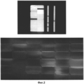
Были получены опытные результаты сканирования солнечных батарей. На представленных примерах (Фиг.2) показаны примеры электрограмм, получаемых с помощью установки лазерного сканирования от двух типов солнечных батарей. На них видны неработающие ФЭП (черный цвет) и цветовые отличия работоспособных ФЭП (различие по уровню мощности).Experimental results from scanning solar cells were obtained. The examples presented (Figure 2) show examples of electrograms obtained using a laser scanning unit from two types of solar panels. They show inactive PECs (black) and color differences of workable PECs (difference in power level).
Совокупность технических решений, примененных в Установке лазерного сканирования, позволяет решить поставленные задачи:The set of technical solutions used in the installation of laser scanning, allows to solve the tasks:
1. получить информацию о распределении энергетических параметров ФЭП в составе исследуемой солнечной батареи в цифровом виде, доступную для дальнейшей обработки с помощью различных приложений для визуализации данных;1. to obtain information on the distribution of the energy parameters of solar cells in the composition of the studied solar battery in digital form, available for further processing using various applications for data visualization;
2. осуществить визуализацию данных, позволяющую быстро оценить работоспособность ФЭП в составе солнечной батареи и распределение их энергетических параметров;2. to visualize the data, allowing you to quickly evaluate the performance of the solar cells in the composition of the solar battery and the distribution of their energy parameters;
3. оценить в процентном отношении предел возможности улучшения удельных энергетических характеристик ФЭП или солнечной батареи.3. to assess as a percentage the limit of the possibility of improving the specific energy characteristics of solar cells or solar cells.
Claims (3)
Priority Applications (1)
| Application Number | Priority Date | Filing Date | Title |
|---|---|---|---|
| RU2013145259/28A RU2565331C2 (en) | 2013-10-10 | 2013-10-10 | Method of investigation spatial distribution of receptivity of characteristics of photoelectric converters in solar panels to optical radiation |
Applications Claiming Priority (1)
| Application Number | Priority Date | Filing Date | Title |
|---|---|---|---|
| RU2013145259/28A RU2565331C2 (en) | 2013-10-10 | 2013-10-10 | Method of investigation spatial distribution of receptivity of characteristics of photoelectric converters in solar panels to optical radiation |
Publications (2)
| Publication Number | Publication Date |
|---|---|
| RU2013145259A RU2013145259A (en) | 2015-04-20 |
| RU2565331C2 true RU2565331C2 (en) | 2015-10-20 |
Family
ID=53282659
Family Applications (1)
| Application Number | Title | Priority Date | Filing Date |
|---|---|---|---|
| RU2013145259/28A RU2565331C2 (en) | 2013-10-10 | 2013-10-10 | Method of investigation spatial distribution of receptivity of characteristics of photoelectric converters in solar panels to optical radiation |
Country Status (1)
| Country | Link |
|---|---|
| RU (1) | RU2565331C2 (en) |
Cited By (1)
| Publication number | Priority date | Publication date | Assignee | Title |
|---|---|---|---|---|
| RU2803315C1 (en) * | 2022-11-01 | 2023-09-12 | Федеральное государственное бюджетное образовательное учреждение высшего образования "Удмуртский государственный университет" | Method of compiling solar module from photovoltaic converters |
Families Citing this family (1)
| Publication number | Priority date | Publication date | Assignee | Title |
|---|---|---|---|---|
| CN108365822B (en) * | 2018-04-12 | 2019-03-22 | 山东大学 | The prediction technique and system of photovoltaic cell working characteristics under the conditions of different illumination temperatures |
Citations (3)
| Publication number | Priority date | Publication date | Assignee | Title |
|---|---|---|---|---|
| US4287473A (en) * | 1979-05-25 | 1981-09-01 | The United States Of America As Represented By The United States Department Of Energy | Nondestructive method for detecting defects in photodetector and solar cell devices |
| WO2010107616A2 (en) * | 2009-03-19 | 2010-09-23 | Kyo Chung | System and method for characterizing solar cell conversion performance and detecting defects in a solar cell |
| RU2476958C2 (en) * | 2011-03-17 | 2013-02-27 | Закрытое Акционерное Общество "ТЕЛЕКОМ-СТВ" | Method of determining voltage-current characteristics of solar cells on solar radiation simulator |
-
2013
- 2013-10-10 RU RU2013145259/28A patent/RU2565331C2/en not_active IP Right Cessation
Patent Citations (3)
| Publication number | Priority date | Publication date | Assignee | Title |
|---|---|---|---|---|
| US4287473A (en) * | 1979-05-25 | 1981-09-01 | The United States Of America As Represented By The United States Department Of Energy | Nondestructive method for detecting defects in photodetector and solar cell devices |
| WO2010107616A2 (en) * | 2009-03-19 | 2010-09-23 | Kyo Chung | System and method for characterizing solar cell conversion performance and detecting defects in a solar cell |
| RU2476958C2 (en) * | 2011-03-17 | 2013-02-27 | Закрытое Акционерное Общество "ТЕЛЕКОМ-СТВ" | Method of determining voltage-current characteristics of solar cells on solar radiation simulator |
Cited By (1)
| Publication number | Priority date | Publication date | Assignee | Title |
|---|---|---|---|---|
| RU2803315C1 (en) * | 2022-11-01 | 2023-09-12 | Федеральное государственное бюджетное образовательное учреждение высшего образования "Удмуртский государственный университет" | Method of compiling solar module from photovoltaic converters |
Also Published As
| Publication number | Publication date |
|---|---|
| RU2013145259A (en) | 2015-04-20 |
Similar Documents
| Publication | Publication Date | Title |
|---|---|---|
| US10533954B2 (en) | Apparatus and methods for combined brightfield, darkfield, and photothermal inspection | |
| US7006212B2 (en) | Electrical circuit conductor inspection | |
| JP5850753B2 (en) | Inspection apparatus and inspection method for optical surface characteristics | |
| US7733111B1 (en) | Segmented optical and electrical testing for photovoltaic devices | |
| JP5319593B2 (en) | Solar cell inspection method and inspection apparatus | |
| JP2012519276A (en) | High-speed quantum efficiency measurement system using solid-state light source | |
| TW200839227A (en) | Automatic inspection system for flat panel substrate | |
| CN103765567A (en) | Method and apparatus for inspection of light emitting semiconductor devices using photoluminescence imaging | |
| KR20100110321A (en) | Inspecting apparatus and inspecting method | |
| JP2013174477A (en) | Test device and test method | |
| CN106970049B (en) | Transmission distribution measuring system and method | |
| CN117517326B (en) | Batch battery piece detection method, device and system of flexible photovoltaic module | |
| KR100863341B1 (en) | Particle inspection system of fpd and wafer using of repetition image | |
| RU2565331C2 (en) | Method of investigation spatial distribution of receptivity of characteristics of photoelectric converters in solar panels to optical radiation | |
| KR101325356B1 (en) | Method and apparatus for measuring properties of solar cell | |
| JP6436672B2 (en) | Inspection apparatus and inspection method | |
| JP5821092B2 (en) | Illuminance distribution measuring apparatus and illuminance distribution measuring method | |
| JP6352715B2 (en) | Inspection apparatus and inspection method | |
| RU2384838C1 (en) | TESTING METHOD OF CHIPS OF CASCADE PHOTOCONVERTERS BASED ON Al-Ga-In-As-P CONNECTIONS AND DEVICE FOR IMPLEMENTATION THEREOF | |
| RU153920U1 (en) | DEVICE FOR CONTROL AND VISUALIZATION OF ENERGY CHARACTERISTICS OF PHOTOELECTRIC CONVERTERS | |
| WO2019234483A1 (en) | Method and system to assess solar cells | |
| KR20180058399A (en) | defect sensing module based on line-beam and defect sensing device using its arrays for detection of the defects on surface | |
| JP4302028B2 (en) | Inspection apparatus and method for transparent electrode film substrate, and program | |
| JP4036712B2 (en) | Nondestructive inspection equipment | |
| TWI818047B (en) | Testing equipment and testing methods |
Legal Events
| Date | Code | Title | Description |
|---|---|---|---|
| MM4A | The patent is invalid due to non-payment of fees |
Effective date: 20161011 |