RU2494579C2 - Production plant for material deposition and electrode for use in it - Google Patents
Production plant for material deposition and electrode for use in it Download PDFInfo
- Publication number
- RU2494579C2 RU2494579C2 RU2010146253/07A RU2010146253A RU2494579C2 RU 2494579 C2 RU2494579 C2 RU 2494579C2 RU 2010146253/07 A RU2010146253/07 A RU 2010146253/07A RU 2010146253 A RU2010146253 A RU 2010146253A RU 2494579 C2 RU2494579 C2 RU 2494579C2
- Authority
- RU
- Russia
- Prior art keywords
- electrode
- outer coating
- contact
- head
- production plant
- Prior art date
Links
Images
Classifications
-
- C—CHEMISTRY; METALLURGY
- C23—COATING METALLIC MATERIAL; COATING MATERIAL WITH METALLIC MATERIAL; CHEMICAL SURFACE TREATMENT; DIFFUSION TREATMENT OF METALLIC MATERIAL; COATING BY VACUUM EVAPORATION, BY SPUTTERING, BY ION IMPLANTATION OR BY CHEMICAL VAPOUR DEPOSITION, IN GENERAL; INHIBITING CORROSION OF METALLIC MATERIAL OR INCRUSTATION IN GENERAL
- C23C—COATING METALLIC MATERIAL; COATING MATERIAL WITH METALLIC MATERIAL; SURFACE TREATMENT OF METALLIC MATERIAL BY DIFFUSION INTO THE SURFACE, BY CHEMICAL CONVERSION OR SUBSTITUTION; COATING BY VACUUM EVAPORATION, BY SPUTTERING, BY ION IMPLANTATION OR BY CHEMICAL VAPOUR DEPOSITION, IN GENERAL
- C23C16/00—Chemical coating by decomposition of gaseous compounds, without leaving reaction products of surface material in the coating, i.e. chemical vapour deposition [CVD] processes
- C23C16/44—Chemical coating by decomposition of gaseous compounds, without leaving reaction products of surface material in the coating, i.e. chemical vapour deposition [CVD] processes characterised by the method of coating
- C23C16/4418—Methods for making free-standing articles
-
- C—CHEMISTRY; METALLURGY
- C01—INORGANIC CHEMISTRY
- C01B—NON-METALLIC ELEMENTS; COMPOUNDS THEREOF; METALLOIDS OR COMPOUNDS THEREOF NOT COVERED BY SUBCLASS C01C
- C01B33/00—Silicon; Compounds thereof
- C01B33/02—Silicon
- C01B33/021—Preparation
- C01B33/027—Preparation by decomposition or reduction of gaseous or vaporised silicon compounds other than silica or silica-containing material
- C01B33/035—Preparation by decomposition or reduction of gaseous or vaporised silicon compounds other than silica or silica-containing material by decomposition or reduction of gaseous or vaporised silicon compounds in the presence of heated filaments of silicon, carbon or a refractory metal, e.g. tantalum or tungsten, or in the presence of heated silicon rods on which the formed silicon is deposited, a silicon rod being obtained, e.g. Siemens process
-
- C—CHEMISTRY; METALLURGY
- C25—ELECTROLYTIC OR ELECTROPHORETIC PROCESSES; APPARATUS THEREFOR
- C25D—PROCESSES FOR THE ELECTROLYTIC OR ELECTROPHORETIC PRODUCTION OF COATINGS; ELECTROFORMING; APPARATUS THEREFOR
- C25D17/00—Constructional parts, or assemblies thereof, of cells for electrolytic coating
- C25D17/10—Electrodes, e.g. composition, counter electrode
- C25D17/12—Shape or form
-
- H—ELECTRICITY
- H01—ELECTRIC ELEMENTS
- H01R—ELECTRICALLY-CONDUCTIVE CONNECTIONS; STRUCTURAL ASSOCIATIONS OF A PLURALITY OF MUTUALLY-INSULATED ELECTRICAL CONNECTING ELEMENTS; COUPLING DEVICES; CURRENT COLLECTORS
- H01R13/00—Details of coupling devices of the kinds covered by groups H01R12/70 or H01R24/00 - H01R33/00
- H01R13/005—Electrical coupling combined with fluidic coupling
-
- H—ELECTRICITY
- H05—ELECTRIC TECHNIQUES NOT OTHERWISE PROVIDED FOR
- H05B—ELECTRIC HEATING; ELECTRIC LIGHT SOURCES NOT OTHERWISE PROVIDED FOR; CIRCUIT ARRANGEMENTS FOR ELECTRIC LIGHT SOURCES, IN GENERAL
- H05B3/00—Ohmic-resistance heating
- H05B3/02—Details
- H05B3/03—Electrodes
Abstract
Description
Родственные заявкиRelated Applications
[0001] Данная заявка испрашивает приоритет и все преимущества по предварительной заявке на патент США №61/044687, которая была подана 14 апреля 2008 года.[0001] This application claims priority and all advantages in provisional application for US patent No. 61/044687, which was filed April 14, 2008.
Область изобретенияField of Invention
[0002] Данное изобретение относится к производственной установке. В частности, данное изобретение относится к электроду, используемому внутри производственной установки.[0002] This invention relates to a production plant. In particular, this invention relates to an electrode used inside a production plant.
Предпосылки изобретенияBACKGROUND OF THE INVENTION
[0003] Производственные установки для осаждения материала на несущую подложку известны в данной области техники. Такие производственные установки включают в себя корпус, который образует камеру. Обычно несущая подложка выполнена практически U-образной и имеет находящиеся на расстоянии друг от друга первый конец и второй конец. Обычно на каждом конце несущей подложки расположено контактное гнездо. Обычно внутри камеры расположены два или более электрода для приема соответствующего контактного гнезда, расположенного соответственно на первом конце и втором конце несущей подложки. Электрод также включает в себя область контакта, которая поддерживает контактное гнездо и, в итоге, несущую подложку, чтобы предотвратить перемещение несущей подложки относительно корпуса. Область контакта является частью электрода, приспособленной находиться в непосредственном контакте с контактным гнездом и обеспечивающей основной путь тока от электрода к контактному гнезду и в несущую подложку.[0003] Production facilities for depositing material on a support substrate are known in the art. Such production facilities include a housing that forms a chamber. Typically, the carrier substrate is substantially U-shaped and has a first end and a second end spaced apart from each other. Typically, a contact socket is located at each end of the carrier substrate. Typically, two or more electrodes are disposed within the chamber to receive a corresponding contact socket located respectively at a first end and a second end of a carrier substrate. The electrode also includes a contact area that supports the contact socket and, ultimately, the carrier substrate, to prevent the carrier substrate from moving relative to the housing. The contact area is part of the electrode, adapted to be in direct contact with the contact socket and providing the main current path from the electrode to the contact socket and to the carrier substrate.
[0004] С электродом соединен источник питания для питания электрическим током несущей подложки. Электрический ток нагревает как электрод, так и несущую подложку. Электрод и несущая подложка каждый имеет некую температуру, причем температура несущей подложки разогревается до температуры осаждения. Обработанная несущая подложка формируется путем осаждения материала на несущую подложку.[0004] A power source is connected to the electrode to supply electric current to the carrier substrate. An electric current heats both the electrode and the carrier substrate. The electrode and the carrier substrate each have a certain temperature, and the temperature of the carrier substrate is heated to the deposition temperature. The treated carrier substrate is formed by depositing material on the carrier substrate.
[0005] Как известно в данной области техники, существуют вариации по форме электрода и контактного гнезда, чтобы учитывать тепловое расширение осажденного на несущую подложку материала при нагревании несущей подложки до температуры осаждения. Один такой способ предполагает использование электрода с плоской головкой и контактного гнезда в виде графитового блока скольжения. Графитовый блок скольжения действует в качестве мостика между несущей подложкой и электродом с плоской головкой. Вес несущей подложки и графитового блока скольжения, действующий на область контакта, уменьшает контактное сопротивление между графитовым блоком скольжения и электродом с плоской головкой. Другой такой способ предполагает использование электрода из двух частей. Электрод из двух частей включает в себя первую половину и вторую половину для сжатия контактного гнезда. С первой половиной и второй половиной электрода из двух частей соединен пружинный элемент для обеспечения силы для сжатия контактного гнезда. Другой такой способ предполагает использование образующего стакан электрода с областью контакта, расположенной внутри части этого стакана. Контактное гнездо приспособлено садиться в стакан электрода и контактировать с областью контакта, расположенной внутри стакана электрода. Альтернативно, электрод может образовывать область контакта на своей наружной поверхности без образовывания стакана, а контактное гнездо может быть выполнено в виде колпака, который садится поверх электрода для контактирования с областью контакта, расположенной на наружной поверхности электрода.[0005] As is known in the art, there are variations in the shape of the electrode and the contact socket in order to take into account the thermal expansion of the material deposited on the carrier substrate when the carrier substrate is heated to the deposition temperature. One such method involves the use of an electrode with a flat head and a contact socket in the form of a graphite slip block. The graphite slip block acts as a bridge between the carrier substrate and the flat-head electrode. The weight of the carrier substrate and the graphite slip block acting on the contact area reduces the contact resistance between the graphite slip block and the flat-head electrode. Another such method involves the use of an electrode in two parts. The two-part electrode includes a first half and a second half for compressing the contact socket. A spring element is connected to the first half and second half of the two-electrode electrode to provide a force to compress the contact socket. Another such method involves the use of forming a glass electrode with a contact area located inside part of this glass. The contact socket is adapted to sit in the electrode cup and contact with the contact area located inside the electrode cup. Alternatively, the electrode may form a contact region on its outer surface without forming a cup, and the contact socket may be in the form of a cap that sits on top of the electrode to contact a contact region located on the outer surface of the electrode.
[0006] На внешней поверхности электрода вне области контакта на той части электрода, которая расположена внутри камеры, происходит зарастание электрода в связи с накоплением отложений. Отложения со временем приводят к ненадлежащей посадке между контактным гнездом и электродом. Ненадлежащая посадка вызывает маленькие электрические дуги между областью контакта и контактным гнездом, что приводит к загрязнению металлом материала, осажденного на несущую подложку. Загрязнение металлом уменьшает ценность несущей подложки, так как осажденный материал является менее чистым. Кроме того, зарастание уменьшает теплопередачу между электродом и контактным гнездом, в результате чего электрод достигает более высоких температур для эффективного нагревания контактного гнезда и, в итоге, несущей подложки. Более высокие температуры электрода приводят к ускоренному осаждению материала на электроде. Это особенно справедливо в случае электродов, которые содержат серебро или медь в качестве единственного или основного присутствующего в них металла.[0006] On the outer surface of the electrode outside the contact area on that part of the electrode that is located inside the chamber, overgrowing of the electrode occurs due to accumulation of deposits. Deposition over time leads to an improper fit between the contact socket and the electrode. An improper fit causes small electric arcs between the contact area and the contact socket, which leads to metal contamination of the material deposited on the supporting substrate. Metal contamination reduces the value of the carrier substrate, since the deposited material is less pure. In addition, overgrowing reduces heat transfer between the electrode and the contact socket, as a result of which the electrode reaches higher temperatures to efficiently heat the contact socket and, ultimately, the carrier substrate. Higher electrode temperatures result in accelerated deposition of material on the electrode. This is especially true for electrodes that contain silver or copper as the sole or primary metal present in them.
[0007] Кроме того, зарастание электрода происходит на внешней поверхности электрода, на той части внешней поверхности, которая находится вне камеры. Такое зарастание отличается от того типа зарастания, которое происходит на той части электрода, которая расположена внутри камеры, что обуславливается используемым для осаждения материалом. Зарастание внешней поверхности электрода, которая находится вне камеры, может быть вызвано производственными условиями вне производственной установки, или может просто обуславливаться окислением в связи с воздействием воздуха на электрод. Это особенно справедливо в случае электродов, которые содержат серебро или медь в качестве единственного или основного присутствующего в них металла.[0007] In addition, electrode overgrowth occurs on the outer surface of the electrode, on that part of the outer surface that is outside the chamber. Such overgrowing is different from the type of overgrowing that occurs on that part of the electrode that is located inside the chamber, which is caused by the material used for deposition. The growth of the outer surface of the electrode, which is located outside the chamber, can be caused by production conditions outside the production plant, or it can simply be caused by oxidation due to the effect of air on the electrode. This is especially true for electrodes that contain silver or copper as the sole or primary metal present in them.
[0008] Электрод должен быть заменен, когда имеет место одно или более из следующих условий: во-первых, когда загрязнение материала, осаждаемого на несущую подложку, превысит пороговый уровень; во-вторых, когда зарастание внешней поверхности электрода в камере вызывает ухудшение соединения между электродом и контактным гнездом; и, в-третьих, когда требуются слишком большие рабочие температуры для электрода в связи с осаждением материала на электроде. Электрод имеет срок службы, определяемый числом несущих подложек, которые электрод может обработать до того, как случится что-то одно из вышеперечисленного.[0008] The electrode must be replaced when one or more of the following conditions occurs: firstly, when the contamination of the material deposited on the supporting substrate exceeds a threshold level; secondly, when the overgrowth of the outer surface of the electrode in the chamber causes a deterioration in the connection between the electrode and the contact socket; and thirdly, when too high operating temperatures are required for the electrode due to the deposition of material on the electrode. The electrode has a service life determined by the number of carrier substrates that the electrode can process before one of the above happens.
[0009] В связи с вышеуказанными проблемами, относящимися к зарастанию электрода, остается потребность в по меньшей мере замедлении зарастания электрода, чтобы улучшить производительность электрода и тем самым увеличить полезный срок службы электрода.[0009] In connection with the above problems related to electrode overgrowth, there remains a need to at least slow down electrode overgrowth in order to improve electrode performance and thereby increase the useful life of the electrode.
Сущность изобретения и преимуществаSummary of invention and advantages
[0010] Данное изобретение относится к производственной установке для осаждения материала на несущую подложку и к электроду для использования с такой производственной установкой. Несущая подложка имеет находящиеся на расстоянии друг от друга первый конец и второй конец. На каждом из концов несущей подложки расположено контактное гнездо.[0010] This invention relates to a production plant for depositing material on a carrier substrate and to an electrode for use with such a production plant. The carrier substrate has a first end and a second end spaced apart from each other. A contact socket is located at each end of the carrier substrate.
[0011] Производственная установка включает в себя корпус, который образует камеру. Через корпус образован впуск для введения газа в камеру. Также через корпус образован выпуск для отведения газа из камеры. По меньшей мере один электрод расположен проходящим через корпус, причем этот электрод по меньшей мере частично расположен внутри камеры для соединения с контактным гнездом. Электрод имеет внешнюю поверхность, имеющую область контакта, которая приспособлена контактировать с контактным гнездом. На внешней поверхности электрода, вне области контакта, расположено внешнее покрытие. Внешнее покрытие имеет электропроводность по меньшей мере 9×10⁶ Сименс/метр и сопротивление коррозии большее, чем у серебра в ряду электродных потенциалов, который основан на использовании морской воды комнатной температуры в качестве электролита. С электродом соединен источник питания для снабжения электрическим током электрода.[0011] The manufacturing plant includes a housing that forms a chamber. An inlet is formed through the housing for introducing gas into the chamber. Also, an outlet for discharging gas from the chamber is formed through the housing. At least one electrode is located passing through the housing, and this electrode is at least partially located inside the chamber for connection with the contact socket. The electrode has an outer surface having a contact area, which is adapted to contact with the contact socket. On the outer surface of the electrode, outside the contact area, there is an outer coating. The outer coating has an electrical conductivity of at least 9 × 10 6 Siemens / meter and corrosion resistance greater than that of silver in the range of electrode potentials, which is based on the use of sea temperature at room temperature as an electrolyte. A power source is connected to the electrode to supply an electrode with electric current.
[0012] Существует много преимуществ регулирования типа и местоположения внешнего покрытия на внешней поверхности электрода. Одним преимуществом является то, что возможно замедлить зарастание электрода путем подбора внешнего покрытия на внешней поверхности электрода в его различных областях с различными материалами в зависимости от источника зарастания. Путем замедления зарастания продлевается срок службы электрода, что приводит к меньшей себестоимости производства и уменьшению длительности производства обработанных несущих подложек. Кроме того, соображения относительно электропроводности представляют меньшую важность вне области контакта на внешней поверхности по сравнению с зоной внутри области контакта, тем самым обеспечивая возможность использовать для внешнего покрытия вне области контакта большее количество вариантов по отношению к типу металла, который может быть в него включен.[0012] There are many advantages to controlling the type and location of the outer coating on the outer surface of the electrode. One advantage is that it is possible to slow down electrode overgrowth by selecting an external coating on the outer surface of the electrode in its various areas with different materials depending on the source of overgrowing. By slowing down overgrowing, the service life of the electrode is extended, which leads to lower production costs and reduced production times for the treated support substrates. In addition, considerations regarding electrical conductivity are less important outside the contact area on the external surface than in the area inside the contact area, thereby making it possible to use a larger number of options for the external coating outside the contact area with respect to the type of metal that can be included in it.
Краткое описание чертежейBrief Description of the Drawings
[0013] Другие преимущества данного изобретения будут без труда оценены, а также станут более понятными при обращении к нижеследующему подробному описанию при рассмотрении вместе с приложенными чертежами, на которых:[0013] Other advantages of this invention will be readily appreciated, and will also become clearer when referring to the following detailed description when considered together with the attached drawings, in which:
[0014] Фигура 1 является видом в сечении производственной установки для осаждения материала на несущую подложку;[0014] Figure 1 is a sectional view of a production plant for depositing material on a carrier substrate;
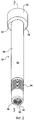
[0015] Фигура 2 является видом в перспективе электрода, используемого с производственной установкой по Фигуре 1;[0015] Figure 2 is a perspective view of an electrode used with the production unit of Figure 1;
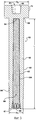
[0016] Фигура 3 является видом в сечении электрода по Фигуре 2, выполненным вдоль линии 3-3 на Фигуре 2;[0016] Figure 3 is a sectional view of the electrode of Figure 2, taken along line 3-3 of Figure 2;
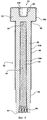
[0017] Фигура 4 является видом в сечении электрода по Фигуре 3, показывающим внешнее покрытие на его внешней поверхности;[0017] Figure 4 is a sectional view of the electrode of Figure 3, showing the outer coating on its outer surface;
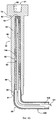
[0018] Фигура 4А является видом в сечении электрода по Фигуре 3 с частью подключенной к нему циркуляционной системы;[0018] Figure 4A is a sectional view of the electrode of Figure 3 with a portion of a circulation system connected thereto;
[0019] Фигура 5 является видом в сечении производственной установки по Фигуре 1 во время осаждения материала на несущую подложку.[0019] Figure 5 is a sectional view of the production plant of Figure 1 during the deposition of material on a carrier substrate.
Подробное описание изобретенияDETAILED DESCRIPTION OF THE INVENTION
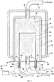
[0020] Обращаясь к Фигурам, на которых похожие номера обозначают похожие или соответствующие части на нескольких видах, производственная установка 20 для осаждения материала 22 на несущую подложку 24 показана на Фигурах 1 и 5. В одном варианте реализации подлежащий осаждению материал 22 является кремнием; тем не менее, следует понимать, что производственная установка 20 может быть использована для осаждения на несущую подложку 24 других материалов без выхода за рамки объема предложенного изобретения.[0020] Turning to the Figures in which like numbers denote similar or corresponding parts in several views, a
[0021] Обычно, при способах химического парофазного осаждения, известных в данной области техники, таких как способ Сименса, несущая подложка 24 выполнена практически U-образной и имеет первый конец 54 и второй конец 56, находящиеся на расстоянии и параллельные друг другу. На каждом из первого конца 54 и второго конца 56 несущей подложки 24 расположено контактное гнездо 57.[0021] Typically, with chemical vapor deposition methods known in the art, such as the Siemens method, the
[0022] Производственная установка 20 включает в себя корпус 28, который образует камеру 30. Обычно, корпус 28 содержит внутренний цилиндр 32, наружный цилиндр 34 и пластину-основание 36. Внутренний цилиндр 32 включает в себя открытый конец 38 и закрытый конец 40, находящиеся на расстоянии друг от друга. Наружный цилиндр 34 расположен вокруг внутреннего цилиндра 32, образуя полость 42 между внутренним цилиндром 32 и наружным цилиндром 34, обычно служащую в качестве рубашки, вмещающей циркулирующую охлаждающую жидкость (не показано). Специалисты в данной области техники должны понимать, что полость 42 может быть традиционной рубашкой сосуда, рубашкой с отражателями или рубашкой из полутрубок, но не ограничивается ими.[0022]
[0023] Пластина-основание 36 расположена на открытом конце 38 внутреннего цилиндра 32, образуя камеру 30. Пластина-основание 36 включает в себя уплотнитель (не показан), расположенный в совмещении с внутренним цилиндром 32 для уплотнения камеры 30, когда внутренний цилиндр 32 располагается на пластине-основании 36. В одном варианте реализации производственная установка 20 представляет собой реактор химического парофазного осаждения типа Сименса.[0023] The
[0024] Корпус 28 образует впуск 44 для введения газа 45 в камеру 30 и выпуск 46 для отведения газа 45 из камеры 30. Обычно, впускной патрубок 48 соединен с впуском 44 для подачи газа 45 в корпус 28, а выпускной патрубок 50 соединен с выпуском 46 для удаления газа 45 из корпуса 28. Выпускной патрубок 50 может быть заключен в рубашку с охлаждающей жидкостью, такой как вода или коммерчески доступная теплопередающая текучая среда.[0024] The
[0025] По меньшей мере один электрод 52 расположен проходящим через корпус 28 для соединения с контактным гнездом 57. В одном варианте реализации этот по меньшей мере один электрод 52 включает в себя первый электрод 52, расположенный проходящим через корпус 28, чтобы принимать контактное гнездо 57 первого конца 54 несущей подложки 24, и второй электрод 52, расположенный проходящим через корпус 28, чтобы принимать контактное гнездо 57 второго конца 56 несущей подложки 24. Следует понимать, что электрод 52 может быть электродом любого типа, известного в данной области техники, таким как, например, электрод с плоской головкой, электрод из двух частей или электрод со стаканом. Кроме того, этот по меньшей мере один электрод 52 по меньшей мере частично расположен внутри камеры 30. В одном варианте реализации электрод 52 расположен проходящим через пластину-основание 36.[0025] At least one
[0026] Электрод 52 содержит электропроводный материал, имеющий минимальную электропроводность при комнатной температуре по меньшей мере 14×106 Сименс/метр или См/м. Например, электрод 52 может содержать по меньшей мере один материал из меди, серебра, никеля, инконели и золота, каждый из которых удовлетворяет изложенным выше параметрам проводимости. Кроме того, электрод 52 может содержать сплав, который удовлетворяет изложенным выше параметрам проводимости. Обычно, электрод 52 содержит электропроводный материал, имеющий минимальную электропроводность при комнатной температуре примерно 58×106 См/м. Обычно, электрод 52 содержит медь, и медь обычно присутствует в количестве примерно 100% по весу в расчете на вес электрода 52. Медь может быть бескислородной электролитической медью марки UNS 10100.[0026] The
[0027] Обращаясь также к Фигурам 2 и 3, электрод 52 имеет внешнюю поверхность 60. Внешняя поверхность 60 электрода 52 имеет область 80 контакта. В частности, область 80 контакта, как она определена здесь, является той частью внешней поверхности 60 электрода 52, которая приспособлена находиться в непосредственном контакте с контактным гнездом 57 и которая обеспечивает основной путь тока от электрода 52 к контактному гнезду 57 и в несущую подложку 24. Как таковая, в нормальном режиме работы производственной установки 20 область 80 контакта экранирована от воздействия материала 22, который осаждают на несущую подложку 24. Так как область 80 контакта приспособлена находиться в непосредственном контакте с контактным гнездом 57 и обычно не подвержена воздействию материала 22 в процессе осаждения на несущую подложку 24, к области 80 контакта применяются иные конструктивные соображения, чем к другим частям электрода 52, причем эти соображения описаны более подробно ниже.[0027] Referring also to Figures 2 and 3, the
[0028] В одном варианте реализации электрод 52 включает в себя ствол 58, имеющий первый конец 61 и второй конец 62. Когда он есть, ствол 58 также образует внешнюю поверхность 60 электрода 52. Обычно, первый конец 61 является открытым концом электрода 52. В одном варианте реализации ствол 58 имеет круглую форму поперечного сечения, что приводит к стволу в форме цилиндра, который образует диаметр D1. Тем не менее, следует понимать, что ствол 58 может иметь прямоугольную, треугольную или эллиптическую форму поперечного сечения без выхода за рамки предложенного изобретения.[0028] In one embodiment, the
[0029] Электрод 52 может также включать в себя головку 72, расположенную на одном из концов 61, 62 ствола 58. Следует понимать, что головка 72 может быть цельной со стволом 58. Обычно, когда головка 72 имеется, головка 72 также образует внешнюю поверхность 60, имеющую область 80 контакта. Специалисты в данной области техники должны понимать, что способ соединения контактного гнезда 57 с электродом 52 может меняться в зависимости от применения без выхода за рамки предложенного изобретения. Например, в одном варианте реализации, таком как в случае электродов с плоской головкой (не показано), область контакта может быть лишь верхней, плоской поверхностью на головке 72 электрода 52, а контактное гнездо 57 может образовывать колпак контактного гнезда (не показан), который садится на головку 72 электрода 52 для контактирования с областью контакта. Альтернативно, хотя это и не показано, головка 72 может отсутствовать на концах 61, 62 ствола 58. В этом варианте реализации электрод 52 может образовывать область контакта на внешней поверхности 60 ствола 58, а контактное гнездо 57 может быть выполнено в виде колпака, который садится на ствол 58 электрода 52 для контактирования с областью 80 контакта, расположенной на внешней поверхности 60 ствола 58.[0029] The
[0030] В другом варианте реализации, как показано на Фигурах 2-4, электрод 52 образует стакан 81 для приема контактного гнезда 57. Когда электрод 52 образует стакан 81, область 80 контакта расположена внутри части стакана 81. Контактное гнездо 57 и стакан 81 могут быть сконструированы так, чтобы контактное гнездо 57 могло быть удалено из электрода 52, когда несущую подложку 24 вытаскивают из производственной установки 20. Обычно, головка 72 образует диаметр D2, который больше диаметра D1 ствола 58. Пластина-основание 36 образует отверстие (не показано) для приема ствола 58 электрода 52, так что головка 72 электрода 52 остается внутри камеры 30 для уплотнения камеры 30. Следует понимать, что головка 72 может быть цельной со стволом 58.[0030] In another embodiment, as shown in Figures 2-4, the
[0031] На внешней поверхности 60 электрода 52 может быть расположена первая резьба 84. Снова обращаясь к Фигурам 1 и 5, вокруг электрода 52 обычно расположена диэлектрическая втулка 86 для изолирования электрода 52. Диэлектрическая втулка 86 может содержать керамику. На первой резьбе 84 расположена гайка 88 для зажатия диэлектрической втулки 86 между пластиной-основанием 36 и гайкой 88, чтобы прикрепить электрод 52 к корпусу 28. Следует понимать, что электрод 52 может быть прикреплен к корпусу 28 другими способами, такими как, например, с помощью фланца, без выхода за рамки объема предложенного изобретения.[0031] A
[0032] Снова обращаясь к Фигурам со 2 по 4, обычно по меньшей мере одно из ствола 58 и головки 72 включает в себя внутреннюю поверхность 62, образующую канал 64. Внутренняя поверхность 62 включает в себя контактный конец 94, находящийся на расстоянии от первого конца 61 ствола 58. Контактный конец 94 является в целом плоским и параллельным первому концу 61 электрода 52. Следует понимать, что могут быть использованы и другие конфигурации контактного конца 94, такие как конфигурация в форме конуса, конфигурация в форме эллипса или конфигурация в форме перевернутого конуса (ни одна из которых не показана). Канал 64 имеет длину L, которая простирается от первого конца 61 электрода до контактного конца 94. Следует понимать, что контактный конец 94 может быть расположен внутри ствола 58 электрода 52, или же контактный конец 94 может быть расположен внутри головки 72 электрода, если она есть, без выхода за рамки предложенного изобретения.[0032] Referring again to Figures 2 to 4, typically at least one of the
[0033] Снова обращаясь к Фигурам 1 и 5, производственная установка 20 дополнительно включает в себя источник 96 питания, соединенный с электродом 52 для снабжения электрическим током электрода 52. Обычно, электрический провод или кабель 97 соединяет источник 96 питания с электродом 52. В одном варианте реализации электрический провод 97 соединен с электродом 52 путем пропускания электрического провода 97 между первой резьбой 84 и гайкой 88. Следует понимать, что соединение электрического провода 97 с электродом 52 может быть осуществлено различными способами.[0033] Referring again to Figures 1 and 5, the
[0034] Электрод 52 имеет температуру, которая изменяется при прохождении через него электрического тока, что приводит к нагреванию электрода 52 и тем самым установлению рабочей температуры электрода. Такое нагревание известно специалистам в данной области техники как джоулев нагрев. В частности, электрический ток проходит через электрод 52, через контактное гнездо 57 и в несущую подложку 24, что приводит к джоулеву нагреву несущей подложки 24. Кроме того, джоулев нагрев несущей подложки 24 приводит к радиационному/конвекционному нагреву камеры 30. Прохождение электрического тока через несущую подложку 24 устанавливает рабочую температуру несущей подложки 24.[0034] The
[0035] Обращаясь к Фигуре 4А и снова к Фигурам 1 и 5, производственная установка 20 может также включать в себя циркуляционную систему 98, расположенную внутри канала 64 электрода 52. Когда она имеется, циркуляционная система 98 может быть по меньшей мере частично расположена внутри канала 64. Следует понимать, что часть циркуляционной системы 98 может быть расположена вне канала 64. На внутренней поверхности 62 электрода 52 может быть расположена вторая резьба 99 для соединения циркуляционной системы 98 с электродом 52. Тем не менее, специалисты в данной области техники должны понимать, что для соединения циркуляционной системы 98 с электродом могут быть использованы и другие способы крепления, такие как использование фланцев или муфт.[0035] Referring to Figure 4A and again to Figures 1 and 5, the
[0036] Циркуляционная система 98 включает в себя охладитель в проточном сообщении с каналом 64 электрода 52 для уменьшения температуры электрода 52. В одном варианте реализации охладитель является водой; тем не менее, следует понимать, что охладитель может быть любой жидкостью, предназначенной для уменьшения тепла за счет циркуляции, без выхода за рамки предложенного изобретения. Более того, циркуляционная система 98 также включает в себя шланг 100, подключенный между электродом 52 и резервуаром (не показан). Обращаясь только к Фигуре 4А, шланг 100 включает в себя внутреннюю трубку 101 и внешнюю трубку 102. Следует понимать, что внутренняя трубка 101 и внешняя трубка 102 могут быть цельными со шлангом 100, или, альтернативно, внутренняя трубка 101 и внешняя трубка 102 могут быть прикреплены к шлангу 100 с использованием муфт (не показано). Внутренняя трубка 101 расположена внутри канала 64 и простирается на большую часть длины L канала 64 для циркуляции охладителя внутри электрода 52.[0036] The
[0037] Охладитель внутри циркуляционной системы 98 находится под давлением, чтобы принудительно направить охладитель через внутреннюю трубку 101 и внешние трубки 102. Обычно, охладитель покидает внутреннюю трубку 101 и принудительно сталкивается с контактным концом 94 внутренней поверхности 62 электрода 52, а затем покидает канал 64 через внешнюю трубку 102 шланга 100. Следует понимать, что также возможно изменение конфигурации потоков на обратную, так что охладитель входит в канал 64 через внешнюю трубку 102, а покидает канал 64 через внутреннюю трубку 101. Специалисты в области теплопередачи должны понимать, что конфигурация контактного конца 94 влияет на скорость теплопередачи в связи с площадью поверхности и близостью к головке 72 электрода 52. Как указано выше, различные геометрические контуры контактного конца 94 приводят к различным коэффициентам конвективной теплопередачи при одинаковой скорости циркуляции.[0037] The cooler inside the
[0038] Обращаясь к Фигуре 4, электрод 52 включает в себя внешнее покрытие 106, расположенное на его внешней поверхности 60 вне области 80 контакта. В частности, внешнее покрытие 106 обычно расположено на по меньшей мере одном из головки 72, вне области 80 контакта, и ствола 58 электрода 52. Другими словами, внешнее покрытие 106 может быть расположено на головке 72 вне области 80 контакта, на стволе 58, или как на головке 72 вне области 80 контакта, так и на стволе 58. Если оно находится на стволе 58, внешнее покрытие 106 может простираться от головки 72 до первой резьбы 84 на стволе 58. Внешнее покрытие 106 имеет электропроводность по меньшей мере 9×10⁶ Сименс/метр, более часто по меньшей мере 20, наиболее часто по меньшей мере 40, и сопротивление коррозии большее, чем у серебра в ряду электрических потенциалов, основанном на использовании морской воды комнатной температуры в качестве электролита. Такие опыты по определению ряда электродных потенциалов хорошо известны в данной области техники. В связи с меньшей важностью электропроводности для внешнего покрытия 106, чем для самого электрода 52, и поскольку внешнее покрытие 106 не предназначено находиться в контакте с несущей подложкой 24 в процессе осаждения, для внешнего покрытия 106 может быть использован более широкий диапазон материалов, чем те, которые могут быть использованы для частей электрода 52, которые не предназначены находиться в контакте с несущей подложкой 24. Кроме того, так как требованиям по электропроводности к внешнему покрытию 106 удовлетворяет более широкий диапазон материалов, чем к частям электрода 52, которые предназначены находиться в контакте с контактным гнездом 57, могут быть выбраны материалы, которые являются более стойкими к коррозии и, таким образом, зарастают медленнее, чем материалы, используемые для самого электрода 52. Более медленное зарастание обеспечивает преимущества относительно увеличения срока службы электрода 52.[0038] Referring to Figure 4, the
[0039] Специальный тип материала, используемый для внешнего покрытия 106, может зависеть от специфического местоположения внешнего покрытия 106. Например, источник коррозии и, следовательно, зарастания может быть разным в зависимости от специфического местоположения внешнего покрытия 106. Когда внешнее покрытие 106 расположено на внешней поверхности 60 головки 72 вне области 80 контакта, внешнее покрытие 106 расположено внутри камеры 30 и, таким образом, подвергается воздействию материала 22, который используется для осаждения на несущую подложку 24. При таких обстоятельствах, для внешнего покрытия 106 может быть желательным обеспечение сопротивления коррозии в хлоридной среде в процессе получения поликристаллического кремния и дополнительное обеспечение сопротивления химическому воздействию при хлорировании и/или силицидировании в результате воздействия материала 22, который используется в ходе процесса осаждения. Подходящие металлы, которые могут быть использованы для внешнего покрытия 106 на головке 72 электрода 52 вне области 80 контакта, включают золото, платину и палладий. Обычно, внешнее покрытие 106 содержит золото в связи с отличным сочетанием электропроводности и сопротивления коррозии от различных источников. Внешнее покрытие 106 может включать в себя и другие металлы при том условии, что по меньшей мере один элемент из золота, платины и палладия включен во внешнее покрытие 106. Например, в одном варианте реализации внешнее покрытие 106 может дополнительно включать в себя по меньшей мере один элемент из серебра, никеля и хрома, такой как сплав никель/серебро. Обычно, внешнее покрытие 106 включает в себя практически только золото, платину и/или палладий. Тем не менее, когда один или более из других металлов присутствуют, общее количество золота, платины и палладия обычно составляет по меньшей мере 50% по весу в расчете на общий вес внешнего покрытия 106. Когда внешнее покрытие 106 расположено на внешней поверхности 60 ствола 58, внешнее покрытие 106 может включать в себя те же или другие металлы из тех, что включены во внешнее покрытие 106 на головке 72 вне области 80 контакта. В одном варианте реализации внешнее покрытие 106 на стволе 58 включает в себя разные материалы с внешней поверхностью 60 головки 72, тем самым позволяя подбирать внешнее покрытие 106 на стволе 58, стойкое к коррозии от иных источников, чем причина коррозии на внешней поверхности 60 головки 72. В другом варианте реализации ствол 58 может не иметь покрытия, расположенного на его внешней поверхности 60. В еще одном другом варианте реализации внешняя поверхность 60 головки может не иметь покрытия, причем внешнее покрытие 106 расположено только на внешней поверхности 60 ствола 58.[0039] The special type of material used for the
[0040] Внешнее покрытие 106 обычно имеет толщину от 0,0254 мм до 0,254 мм, более часто от 0,0508 мм до 0,254 мм, и наиболее часто от 0,127 мм до 0,254 мм.[0040] The
[0041] Электрод 52 может быть покрыт в других местах, отличных от внешней поверхности 60, для продления срока службы электрода 52. Обращаясь к Фигурам со 2 по 4, на внутренней поверхности 62 электрода 52 может быть расположено покрытие 104 канала для сохранения теплопроводности между электродом 52 и охладителем. В общем, покрытие 104 канала имеет большее сопротивление коррозии, которая вызвана взаимодействием охладителя с внутренней поверхностью 62, по сравнению с сопротивлением коррозии электрода 52. Покрытие 104 канала обычно включает в себя металл, который противодействует коррозии и который ингибирует накопление отложений. Например, покрытие 104 канала может содержать по меньшей мере один элемент из серебра, золота, никеля и хрома. Обычно, покрытие 104 канала является никелем. Покрытие 104 канала имеет теплопроводность от 70,3 до 427 Вт/м∙К, более часто от 70,3 до 405 Вт/м∙К, а наиболее часто от 70,3 до 90,5 Вт/м∙К. Покрытие 104 канала также имеет толщину от 0,0025 мм до 0,026 мм, более часто от 0,0025 мм до 0,0127 мм, а наиболее часто от 0,0051 мм до 0,0127 мм.[0041] The
[0042] Кроме того, следует понимать, что электрод 52 может также включать в себя препятствующий потускнению слой, расположенный на покрытии 104 канала. Препятствующий потускнению слой является защитным тонкопленочным органическим слоем, который нанесен поверх покрытия 104 канала. Защитные системы, такие как Tarniban™ фирмы Technic Inc., могут быть использованы после формирования покрытия 104 канала электрода 52, чтобы уменьшить окисление металла в электроде 52 и в покрытии 104 канала, не создавая чрезмерного теплового сопротивления. Например, в одном варианте реализации электрод 52 может содержать серебро, а покрытие 104 канала может содержать серебро с препятствующим потускнению слоем, присутствующим для обеспечения улучшенного сопротивления образованию отложений по сравнению с чистым серебром. Обычно, электрод 52 содержит медь, а покрытие 104 канала содержит никель для максимизации теплопроводности и сопротивления образованию отложений, с препятствующим потускнению слоем, расположенным на покрытии 104 канала.[0042] In addition, it should be understood that the
[0043] Не углубляясь в теорию, замедление зарастания, приписываемое присутствию покрытия 104 канала, продлевает срок службы электрода 52. Увеличение срока службы электрода 52 уменьшает себестоимость производства, так как электрод 52 нужно заменять реже по сравнению с электродами 52 без покрытия 104 канала. Кроме того, длительность производства по осаждению материала 22 на несущую подложку 24 также уменьшается, так как замена электродов 52 производится реже по сравнению с ситуацией, когда используются электроды 52 без покрытия 104 канала. Покрытие 104 канала приводит к уменьшению времени простоя производственной установки 20.[0043] Without delving into the theory, the growth inhibition attributed to the presence of the
[0044] В одном варианте реализации электрод 52 включает в себя покрытие 110 области контакта, расположенное в области 80 контакта электрода 52. Покрытие 110 области контакта обычно содержит металл. Например, покрытие 110 области контакта может содержать по меньшей мере один элемент из серебра, золота, никеля и хрома. Обычно покрытие 110 области контакта содержит никель или серебро. Покрытие 110 области контакта имеет толщину от 0,00254 до 0,254 мм, более часто от 0,00508 мм до 0,127 мм, а наиболее часто от 0,00508 мм до 0,0254 мм. Выбор специального типа металла может зависеть от химической природы газа, тепловых условий вблизи электрода 52 в связи с тем, что сочетание температуры несущей подложки 24, протекающего через электрод 52 электрического тока, расхода охлаждающей жидкости и температуры охлаждающей жидкости могут все влиять на выбор металлов, используемых в различных секциях электрода. Например, когда внешнее покрытие 106 расположено на головке 72 вне области 80 контакта, внешнее покрытие 106 может содержать никель или хром в связи с сопротивлением хлорированию, тогда как использование серебра для покрытия 110 области контакта может быть выбрано из-за сопротивления силицидированию помимо естественного сопротивления хлоридному воздействию. Кроме того, так как серебро является более электропроводным, чем никель или хром, серебро может лучше подойти для покрытия 110 области контакта, чем никель или хром, при том, что электропроводность представляет меньшую важность вне области 80 контакта.[0044] In one embodiment, the
[0045] Покрытие 110 области контакта также обеспечивает улучшенную электрическую проводимость и минимизирует накопление силицида меди внутри области 80 контакта. Накопление силицида меди мешает должной посадке между контактным гнездом 57 и областью 80 контакта, что может привести к точечной коррозии контактного гнезда 57. Точечная коррозия приводит к возникновению маленьких электрических дуг между областью 80 контакта и контактным гнездом 57, что приводит к загрязнению металлом продукта - поликристаллического кремния.[0045] The
[0046] Следует понимать, что в дополнение к внешнему покрытию 106 электрод 52 может иметь по меньшей мере одно из покрытия 104 канала и покрытия 110 области контакта в любом сочетании. Покрытие 104 канала, внешнее покрытие 106 и покрытие 110 области контакта могут быть сформированы путем электроосаждения (гальваностегии). Тем не менее, следует понимать, что каждое из этих покрытий может быть сформировано различными способами без выхода за рамки предложенного изобретения. Также, специалисты в области производства полупроводниковых материалов высокой чистоты, таких как поликристаллический кремний, должны понимать, что некоторые процессы нанесения используют материалы, которые являются легирующими примесями, например, элементы III группы и V группы (за исключением азота для случая производства поликристаллического кремния), и выбор подходящего способа нанесения покрытия может минимизировать потенциальное загрязнение несущей подложки 24. Например, желательно, чтобы зоны электрода, обычно расположенные внутри камеры 32, такие как покрытие 108 головки и покрытие 110 области контакта, имели минимальные включения бора и фосфора в их соответствующие электродные покрытия.[0046] It should be understood that in addition to the
[0047] Типичный способ осаждения материала 22 на несущую подложку 24 обсуждается ниже со ссылкой на Фигуру 5. Несущую подложку 24 помещают внутрь камеры 30 так, чтобы контактные гнезда 57, расположенные на первом конце 54 и втором конце 56 несущей подложки 24, были расположены внутри стакана 81 электрода 52, и камеру 30 герметизируют. Пропускают электрический ток от источника 96 питания к электроду 52. Температуру осаждения рассчитывают, исходя из подлежащего осаждению материала 22. Рабочая температура несущей подложки 24 увеличивается при непосредственном прохождении электрического тока в несущей подложке 24, так что рабочая температура несущей подложки 24 превышает температуру осаждения. Газ 45 вводят в камеру 30, как только несущая подложка 24 достигает температуры осаждения. В одном варианте реализации газ 45, вводимый в камеру 30, содержит галоидсилан, такой как хлорсилан или бромсилан. Газ может дополнительно содержать водород. Тем не менее, следует понимать, что данное изобретение не ограничено присутствующими в газе компонентами и что газ может содержать другие предшественники осаждения, в частности, содержащие кремний молекулы, такие как силан, тетрахлорид кремния и трибромсилан. В одном варианте реализации несущая подложка 24 является тонким стержнем кремния, а производственная установка 20 может быть использована для осаждения кремния на него. В частности, в этом варианте реализации в состав газа обычно входит трихлорсилан, а кремний осаждают на несущую подложку 24 в результате термического разложения трихлорсилана. Охладитель используют для предотвращения достижения рабочей температурой электрода 52 температуры осаждения, чтобы гарантировать отсутствие осаждения кремния на электрод 52. Материал 22 осаждают равномерно на несущую подложку 24 до тех пор, пока не будет достигнут желаемый диаметр материала 22 на несущей подложке 24.[0047] A typical method of depositing
[0048] Как только несущая подложка 24 обработана, электрический ток прерывают, так что электрод 52 и несущая подложка 24 перестают получать электрический ток. Газ 45 отводят через выпуск 46 корпуса 28, и несущей подложке 24 дают охладиться. Как только рабочая температура обработанной несущей подложки 24 понизилась, обработанная несущая подложка 24 может быть вынута из камеры 30. Обработанную несущую подложку 24 затем вынимают, а в производственную установку 20 помещают новую несущую подложку 24.[0048] As soon as the
[0049] Очевидно, в свете вышеприведенных указаний возможны многочисленные модификации и вариации данного изобретения. Вышеуказанное изобретение было описано согласно соответствующим требованиям законодательства; таким образом, описание является по сути скорее примерным, чем ограничивающим. Вариации и модификации раскрытого варианта реализации могут стать ясны специалистам в данной области техники и входят в рамки объема изобретения. Соответственно, объем правовой охраны, предусмотренный этим изобретением, может быть определен только при изучении приведенной далее формулы изобретения.[0049] Obviously, in light of the above indications, numerous modifications and variations of the present invention are possible. The above invention has been described in accordance with the relevant requirements of the law; thus, the description is essentially indicative rather than limiting. Variations and modifications of the disclosed embodiment may become apparent to those skilled in the art and are within the scope of the invention. Accordingly, the scope of legal protection provided by this invention can only be determined by studying the following claims.
Claims (28)
корпус, образующий камеру;
впуск, образованный через упомянутый корпус, для введения газа в камеру;
выпуск, образованный через упомянутый корпус, для отведения газа из камеры;
по меньшей мере один электрод, имеющий внешнюю поверхность, имеющую область контакта, приспособленную контактировать с контактным гнездом, причем упомянутый электрод расположен проходящим через упомянутый корпус, причем упомянутый электрод по меньшей мере частично расположен внутри камеры для соединения с контактным гнездом;
источник питания, соединенный с упомянутым электродом, для снабжения электрическим током упомянутого электрода; и
внешнее покрытие, расположенное на упомянутой внешней поверхности упомянутого электрода вне упомянутой области контакта, причем упомянутое внешнее покрытие имеет электропроводность по меньшей мере 9·106 См/м и сопротивление коррозии большее, чем у серебра в ряду электродных потенциалов, основанном на использовании морской воды комнатной температуры в качестве электролита.1. A production plant for depositing material on a carrier substrate having a first end and a second end spaced apart from one another with a contact socket located at each end of the carrier substrate, said installation comprising:
a housing forming a chamber;
an inlet formed through said housing for introducing gas into the chamber;
an outlet formed through said housing for discharging gas from the chamber;
at least one electrode having an outer surface having a contact area adapted to contact with a contact socket, said electrode being located passing through said housing, said electrode being at least partially located inside a chamber for connecting to a contact socket;
a power source connected to said electrode for supplying electric current to said electrode; and
an outer coating located on said outer surface of said electrode outside said contact region, said outer coating having an electrical conductivity of at least 9 · 10 6 S / m and corrosion resistance greater than that of silver in a series of electrode potentials based on the use of room sea water temperature as an electrolyte.
ствол, имеющий первый конец и второй конец; и
головку, расположенную на одном из упомянутых концов упомянутого ствола.2. The production plant according to claim 1, wherein said electrode further includes:
a trunk having a first end and a second end; and
a head located at one of said ends of said barrel.
ствол, имеющий первый конец и второй конец;
головку, расположенную на одном из упомянутых концов упомянутого ствола, для соединения с контактным гнездом;
при этом упомянутый ствол и упомянутая головка имеют внешнюю поверхность, имеющую область контакта, приспособленную контактировать с контактным гнездом; и
упомянутый электрод имеет внешнюю поверхность и внешнее покрытие, расположенное на упомянутой внешней поверхности вне упомянутой области контакта, причем упомянутое внешнее покрытие имеет электропроводность по меньшей мере 9·106 См/м и сопротивление коррозии большее, чем у серебра в ряду электродных потенциалов, основанном на использовании морской воды комнатной температуры в качестве электролита.14. An electrode for use with a production plant for depositing material on a carrier substrate, said carrier substrate having a first end and a second end spaced apart from one another with a contact socket located at each end of the carrier substrate, said electrode comprising:
a trunk having a first end and a second end;
a head located at one of said ends of said barrel for connection to a contact socket;
wherein said barrel and said head have an external surface having a contact area adapted to contact with the contact socket; and
said electrode has an outer surface and an outer coating located on said outer surface outside said contact area, said outer coating having an electrical conductivity of at least 9 · 10 6 S / m and corrosion resistance greater than that of silver in a series of electrode potentials based on using seawater at room temperature as an electrolyte.
Applications Claiming Priority (3)
| Application Number | Priority Date | Filing Date | Title |
|---|---|---|---|
| US4468708P | 2008-04-14 | 2008-04-14 | |
| US61/044,687 | 2008-04-14 | ||
| PCT/US2009/002294 WO2009128888A1 (en) | 2008-04-14 | 2009-04-13 | Manufacturing apparatus for depositing a material and an electrode for use therein |
Publications (2)
| Publication Number | Publication Date |
|---|---|
| RU2010146253A RU2010146253A (en) | 2012-05-20 |
| RU2494579C2 true RU2494579C2 (en) | 2013-09-27 |
Family
ID=40791646
Family Applications (1)
| Application Number | Title | Priority Date | Filing Date |
|---|---|---|---|
| RU2010146253/07A RU2494579C2 (en) | 2008-04-14 | 2009-04-13 | Production plant for material deposition and electrode for use in it |
Country Status (10)
| Country | Link |
|---|---|
| US (2) | US8951352B2 (en) |
| EP (1) | EP2266369B1 (en) |
| JP (2) | JP5959198B2 (en) |
| KR (1) | KR101552501B1 (en) |
| CN (1) | CN102047751B (en) |
| AU (1) | AU2009236679B2 (en) |
| CA (1) | CA2721095A1 (en) |
| RU (1) | RU2494579C2 (en) |
| TW (1) | TWI505743B (en) |
| WO (1) | WO2009128888A1 (en) |
Families Citing this family (4)
| Publication number | Priority date | Publication date | Assignee | Title |
|---|---|---|---|---|
| EP2266368B1 (en) | 2008-04-14 | 2018-03-28 | Hemlock Semiconductor Operations LLC | Manufacturing apparatus for depositing a material on an electrode for use therein |
| JP5477145B2 (en) * | 2009-04-28 | 2014-04-23 | 三菱マテリアル株式会社 | Polycrystalline silicon reactor |
| JP5699060B2 (en) * | 2011-09-20 | 2015-04-08 | 信越化学工業株式会社 | Method for producing polycrystalline silicon |
| CN107820650B (en) * | 2015-04-14 | 2022-02-18 | 安费诺有限公司 | Electrical connector |
Citations (5)
| Publication number | Priority date | Publication date | Assignee | Title |
|---|---|---|---|---|
| RU2020777C1 (en) * | 1991-07-03 | 1994-09-30 | Нижегородский научно-исследовательский приборостроительный институт "Кварц" | Fluoroplastic substrate metallization deposition method |
| RU2052538C1 (en) * | 1993-04-08 | 1996-01-20 | Сергей Николаевич Кучанов | Method for vacuum deposition of metallized coating on dielectric substrates |
| WO2001060121A1 (en) * | 2000-02-10 | 2001-08-16 | Schott Glas | Electrode for heating a melt, especially a glass melt |
| US20030021894A1 (en) * | 2001-07-30 | 2003-01-30 | Komatsu Ltd. | Method of producing high-purity polycrystallin silicon |
| WO2003107720A1 (en) * | 2002-06-12 | 2003-12-24 | Johnson Matthey Public Limited Company | Improvements in coated equipment, more especially coated ceramic articles |
Family Cites Families (62)
| Publication number | Priority date | Publication date | Assignee | Title |
|---|---|---|---|---|
| GB1054141A (en) | 1900-01-01 | |||
| US1738828A (en) * | 1925-03-02 | 1929-12-10 | Jackson Arthur Hews | Low-resistance permanent wire |
| US3330251A (en) | 1955-11-02 | 1967-07-11 | Siemens Ag | Apparatus for producing highest-purity silicon for electric semiconductor devices |
| US3011877A (en) | 1956-06-25 | 1961-12-05 | Siemens Ag | Production of high-purity semiconductor materials for electrical purposes |
| NL124690C (en) | 1958-05-29 | |||
| DE1150366B (en) | 1958-12-09 | 1963-06-20 | Siemens Ag | Process for the production of hyperpure silicon |
| NL251143A (en) | 1959-05-04 | |||
| DE1155759B (en) | 1959-06-11 | 1963-10-17 | Siemens Ag | Device for obtaining the purest crystalline semiconductor material for electrotechnical purposes |
| DE1264400B (en) | 1961-01-26 | 1968-03-28 | Siemens Ag | Device for the extraction of pure semiconductor material from the gas phase |
| DE1223804B (en) * | 1961-01-26 | 1966-09-01 | Siemens Ag | Device for the extraction of pure semiconductor material, such as silicon |
| DE1138481C2 (en) | 1961-06-09 | 1963-05-22 | Siemens Ag | Process for the production of semiconductor arrangements by single-crystal deposition of semiconductor material from the gas phase |
| DE2324365C3 (en) | 1973-05-14 | 1978-05-11 | Siemens Ag, 1000 Berlin Und 8000 Muenchen | Reaction vessel for depositing semiconductor material on heated substrates |
| DE2541215C3 (en) | 1975-09-16 | 1978-08-03 | Wacker-Chemitronic Gesellschaft Fuer Elektronik-Grundstoffe Mbh, 8263 Burghausen | Process for the production of hollow silicon bodies |
| DE2652218A1 (en) | 1976-11-16 | 1978-05-24 | Wacker Chemitronic | PROCESS FOR PRODUCING SUBSTRATE-BOND LARGE-AREA SILICON |
| JPS53106626A (en) * | 1977-03-02 | 1978-09-16 | Komatsu Mfg Co Ltd | Method of making high purity rod silicon and appratus therefor |
| JPS53108029A (en) | 1977-03-03 | 1978-09-20 | Komatsu Mfg Co Ltd | Method of making high purity silicon having uniform shape |
| US4173944A (en) | 1977-05-20 | 1979-11-13 | Wacker-Chemitronic Gesellschaft Fur Elektronik-Grundstoffe Mbh | Silverplated vapor deposition chamber |
| US4179530A (en) * | 1977-05-20 | 1979-12-18 | Wacker-Chemitronic Gesellschaft Fur Elektronik-Grundstoffe Mbh | Process for the deposition of pure semiconductor material |
| DE2912661C2 (en) | 1979-03-30 | 1982-06-24 | Wacker-Chemitronic Gesellschaft Fuer Elektronik-Grundstoffe Mbh, 8263 Burghausen | Process for the deposition of pure semiconductor material and nozzle for carrying out the process |
| US4304641A (en) | 1980-11-24 | 1981-12-08 | International Business Machines Corporation | Rotary electroplating cell with controlled current distribution |
| US4477911A (en) | 1982-12-02 | 1984-10-16 | Westinghouse Electric Corp. | Integral heat pipe-electrode |
| US4481232A (en) | 1983-05-27 | 1984-11-06 | The United States Of America As Represented By The Department Of Energy | Method and apparatus for producing high purity silicon |
| US4466864A (en) * | 1983-12-16 | 1984-08-21 | At&T Technologies, Inc. | Methods of and apparatus for electroplating preselected surface regions of electrical articles |
| US4822641A (en) * | 1985-04-30 | 1989-04-18 | Inovan Gmbh & Co. Kg | Method of manufacturing a contact construction material structure |
| SE452862B (en) | 1985-06-05 | 1987-12-21 | Aga Ab | LIGHT BAGS LEAD |
| US4707225A (en) | 1986-01-06 | 1987-11-17 | Rockwell International Corporation | Fluid-cooled channel construction |
| US4805556A (en) | 1988-01-15 | 1989-02-21 | Union Carbide Corporation | Reactor system and method for forming uniformly large-diameter polycrystalline rods by the pyrolysis of silane |
| US5096550A (en) | 1990-10-15 | 1992-03-17 | The United States Of America As Represented By The United States Department Of Energy | Method and apparatus for spatially uniform electropolishing and electrolytic etching |
| US5139890A (en) * | 1991-09-30 | 1992-08-18 | Olin Corporation | Silver-coated electrical components |
| US5906799A (en) | 1992-06-01 | 1999-05-25 | Hemlock Semiconductor Corporation | Chlorosilane and hydrogen reactor |
| US5227041A (en) | 1992-06-12 | 1993-07-13 | Digital Equipment Corporation | Dry contact electroplating apparatus |
| DE4243570C1 (en) | 1992-12-22 | 1994-01-27 | Heraeus Gmbh W C | Electrical contact body - has layer sequence comprising base material, contact layer, and thin, galvanically deposited surface layer contg. Gold@ |
| US5422088A (en) | 1994-01-28 | 1995-06-06 | Hemlock Semiconductor Corporation | Process for hydrogenation of tetrachlorosilane |
| JP3377849B2 (en) | 1994-02-02 | 2003-02-17 | 日本エレクトロプレイテイング・エンジニヤース株式会社 | Wafer plating equipment |
| DE4424929C2 (en) | 1994-07-14 | 1997-02-13 | Wacker Chemie Gmbh | Holder for carrier bodies in a device for the deposition of semiconductor material |
| US5567300A (en) | 1994-09-02 | 1996-10-22 | Ibm Corporation | Electrochemical metal removal technique for planarization of surfaces |
| FR2741227A1 (en) | 1995-11-14 | 1997-05-16 | Verrerie & Cristallerie | Long life electrode esp. for glass melting furnace |
| US5911619A (en) | 1997-03-26 | 1999-06-15 | International Business Machines Corporation | Apparatus for electrochemical mechanical planarization |
| US5807165A (en) | 1997-03-26 | 1998-09-15 | International Business Machines Corporation | Method of electrochemical mechanical planarization |
| NL1005963C2 (en) | 1997-05-02 | 1998-11-09 | Asm Int | Vertical oven for treating semiconductor substrates. |
| RU2135629C1 (en) | 1997-11-12 | 1999-08-27 | Государственное предприятие ВНИИавтогенмаш | Method of increasing service life of electrode and nozzle devices and process plasma generator for its embodiment |
| US6544333B2 (en) * | 1997-12-15 | 2003-04-08 | Advanced Silicon Materials Llc | Chemical vapor deposition system for polycrystalline silicon rod production |
| WO1999031013A1 (en) * | 1997-12-15 | 1999-06-24 | Advanced Silicon Materials, Inc. | Chemical vapor deposition system for polycrystalline silicon rod production |
| US6004880A (en) | 1998-02-20 | 1999-12-21 | Lsi Logic Corporation | Method of single step damascene process for deposition and global planarization |
| US6176992B1 (en) | 1998-11-03 | 2001-01-23 | Nutool, Inc. | Method and apparatus for electro-chemical mechanical deposition |
| US6284312B1 (en) | 1999-02-19 | 2001-09-04 | Gt Equipment Technologies Inc | Method and apparatus for chemical vapor deposition of polysilicon |
| JP4372918B2 (en) | 1999-06-30 | 2009-11-25 | パナソニック電工株式会社 | Plasma processing apparatus and plasma processing method |
| JP2001156042A (en) | 1999-11-29 | 2001-06-08 | Hitachi Ltd | Plasma processing apparatus |
| DE10041564C2 (en) | 2000-08-24 | 2002-06-27 | Heraeus Noblelight Gmbh | Coolable infrared radiator element |
| DE10101040A1 (en) | 2001-01-11 | 2002-07-25 | Wacker Chemie Gmbh | Device and method for producing a polycrystalline silicon rod |
| JP2002231357A (en) * | 2001-02-06 | 2002-08-16 | Nagano Fujitsu Component Kk | Electrical contact and connector |
| JP4402860B2 (en) | 2001-03-28 | 2010-01-20 | 忠弘 大見 | Plasma processing equipment |
| JP2002313533A (en) * | 2001-04-17 | 2002-10-25 | Toshiba Ceramics Co Ltd | Planar ceramic heater |
| JP3870824B2 (en) * | 2001-09-11 | 2007-01-24 | 住友電気工業株式会社 | SUBSTRATE HOLDER, SENSOR FOR SEMICONDUCTOR MANUFACTURING DEVICE, AND PROCESSING DEVICE |
| JP2004205059A (en) | 2002-12-20 | 2004-07-22 | Toyo Radiator Co Ltd | Method of manufacturing high erosion resistance heat exchanger |
| JP2005272965A (en) * | 2004-03-25 | 2005-10-06 | Sumitomo Heavy Ind Ltd | Electrode member and deposition system equipped therewith |
| JP4031782B2 (en) | 2004-07-01 | 2008-01-09 | 株式会社大阪チタニウムテクノロジーズ | Polycrystalline silicon manufacturing method and seed holding electrode |
| JP2007281161A (en) | 2006-04-06 | 2007-10-25 | Sumitomo Electric Ind Ltd | Wafer holder for semiconductor manufacturing apparatus, and semiconductor manufacturing apparatus |
| US9683286B2 (en) | 2006-04-28 | 2017-06-20 | Gtat Corporation | Increased polysilicon deposition in a CVD reactor |
| KR100768148B1 (en) | 2006-05-22 | 2007-10-17 | 한국화학연구원 | Methods for preparation of high-purity poly-silicon rods using metallic core means |
| AU2009236677B2 (en) | 2008-04-14 | 2012-11-22 | Hemlock Semiconductor Corporation | Manufacturing apparatus for depositing a material and an electrode for use therein |
| EP2266368B1 (en) | 2008-04-14 | 2018-03-28 | Hemlock Semiconductor Operations LLC | Manufacturing apparatus for depositing a material on an electrode for use therein |
-
2009
- 2009-04-13 CN CN200980120357.0A patent/CN102047751B/en not_active Expired - Fee Related
- 2009-04-13 US US12/937,802 patent/US8951352B2/en not_active Expired - Fee Related
- 2009-04-13 CA CA2721095A patent/CA2721095A1/en not_active Abandoned
- 2009-04-13 RU RU2010146253/07A patent/RU2494579C2/en not_active IP Right Cessation
- 2009-04-13 JP JP2011505007A patent/JP5959198B2/en not_active Expired - Fee Related
- 2009-04-13 KR KR1020107025442A patent/KR101552501B1/en active IP Right Grant
- 2009-04-13 EP EP09732543.5A patent/EP2266369B1/en not_active Not-in-force
- 2009-04-13 AU AU2009236679A patent/AU2009236679B2/en not_active Ceased
- 2009-04-13 WO PCT/US2009/002294 patent/WO2009128888A1/en active Application Filing
- 2009-04-14 TW TW098112368A patent/TWI505743B/en not_active IP Right Cessation
-
2014
- 2014-08-15 US US14/460,843 patent/US20140353147A1/en not_active Abandoned
- 2014-09-19 JP JP2014191023A patent/JP5909533B2/en active Active
Patent Citations (5)
| Publication number | Priority date | Publication date | Assignee | Title |
|---|---|---|---|---|
| RU2020777C1 (en) * | 1991-07-03 | 1994-09-30 | Нижегородский научно-исследовательский приборостроительный институт "Кварц" | Fluoroplastic substrate metallization deposition method |
| RU2052538C1 (en) * | 1993-04-08 | 1996-01-20 | Сергей Николаевич Кучанов | Method for vacuum deposition of metallized coating on dielectric substrates |
| WO2001060121A1 (en) * | 2000-02-10 | 2001-08-16 | Schott Glas | Electrode for heating a melt, especially a glass melt |
| US20030021894A1 (en) * | 2001-07-30 | 2003-01-30 | Komatsu Ltd. | Method of producing high-purity polycrystallin silicon |
| WO2003107720A1 (en) * | 2002-06-12 | 2003-12-24 | Johnson Matthey Public Limited Company | Improvements in coated equipment, more especially coated ceramic articles |
Also Published As
| Publication number | Publication date |
|---|---|
| KR101552501B1 (en) | 2015-09-14 |
| TW201004460A (en) | 2010-01-16 |
| CA2721095A1 (en) | 2009-10-22 |
| KR20110009146A (en) | 2011-01-27 |
| EP2266369A1 (en) | 2010-12-29 |
| WO2009128888A1 (en) | 2009-10-22 |
| AU2009236679A1 (en) | 2009-10-22 |
| JP5959198B2 (en) | 2016-08-02 |
| US20140353147A1 (en) | 2014-12-04 |
| EP2266369B1 (en) | 2017-11-22 |
| US8951352B2 (en) | 2015-02-10 |
| JP5909533B2 (en) | 2016-04-26 |
| US20110036294A1 (en) | 2011-02-17 |
| TWI505743B (en) | 2015-10-21 |
| AU2009236679B2 (en) | 2014-02-27 |
| JP2011523758A (en) | 2011-08-18 |
| JP2015028217A (en) | 2015-02-12 |
| CN102047751B (en) | 2014-01-29 |
| CN102047751A (en) | 2011-05-04 |
| RU2010146253A (en) | 2012-05-20 |
Similar Documents
| Publication | Publication Date | Title |
|---|---|---|
| RU2494578C2 (en) | Production plant for material deposition and electrode for use | |
| RU2503905C2 (en) | Production plant for deposition of material and electrode for use in it | |
| RU2494579C2 (en) | Production plant for material deposition and electrode for use in it | |
| US20120199069A1 (en) | Cvd apparatus |
Legal Events
| Date | Code | Title | Description |
|---|---|---|---|
| MM4A | The patent is invalid due to non-payment of fees |
Effective date: 20160414 |