RU2425402C1 - Integrated optical element and method of making said element - Google Patents
Integrated optical element and method of making said element Download PDFInfo
- Publication number
- RU2425402C1 RU2425402C1 RU2009145607/28A RU2009145607A RU2425402C1 RU 2425402 C1 RU2425402 C1 RU 2425402C1 RU 2009145607/28 A RU2009145607/28 A RU 2009145607/28A RU 2009145607 A RU2009145607 A RU 2009145607A RU 2425402 C1 RU2425402 C1 RU 2425402C1
- Authority
- RU
- Russia
- Prior art keywords
- substrate
- salts
- layer
- optical
- photomask
- Prior art date
Links
Images
Landscapes
- Optical Integrated Circuits (AREA)
Abstract
Description
Изобретение относится к области интегральной оптики, а именно к способам создания оптических канальных волноводов и интегрально-оптических элементов (ИОЭ), и может быть использовано в волноводных оптоэлектронных устройствах, в частности, в качестве пассивных и активных ИОЭ волоконно-оптических датчиков.The invention relates to the field of integrated optics, and in particular to methods for creating optical channel waveguides and integrated optical elements (IOE), and can be used in waveguide optoelectronic devices, in particular, as passive and active IOE fiber optic sensors.
Известен ИОЭ, состоящий из оптического титанового канального волновода и подложки из монокристалла ниобата лития, и способ изготовления таких ИОЭ (Патент ЕПВ №1224492, МПК G02B 6/134; G02B 6/12; G02B 6/13, дата публикации 24.09.2003; Патент РФ №2089928, МПК G02B 6/13, дата приоритета 28.09.1994, дата публикации 10.09.1997), который заключается в нанесении титановой полоски на поверхность образца кристаллической подложки (ниобат лития) и диффузии атомов титана в кристаллическую подложку, которая проводится герметично от окружающей среды под давлением в нагретой и насыщенной кислородом атмосфере с поддержанием температуры (1050°С) и давления в диффузионный период (6-7 часов) и охлаждением окружающей среды. После этого образец подвергают отжигу.Known IOE, consisting of an optical titanium channel waveguide and a substrate of lithium niobate single crystal, and a method of manufacturing such IOE (EPO Patent No. 1224492, IPC G02B 6/134; G02B 6/12; G02B 6/13, publication date 09/24/2003; Patent RF №2089928, IPC G02B 6/13, priority date 09/09/1994, publication date 09/10/1997), which consists in applying a titanium strip to the surface of a sample of a crystalline substrate (lithium niobate) and diffusion of titanium atoms into a crystalline substrate, which is hermetically sealed from environment under pressure in heated and saturated kis Orod atmosphere maintaining the temperature (1050 ° C) and pressure to the diffusion period (6-7 hours) and the surrounding cooling medium. After that, the sample is annealed.
Недостатком такого ИОЭ является подверженность оптического титан-диффузионного волновода высоким оптическим повреждениям, приводящим к росту потерь готового ИОЭ. Необходимость использования столь высоких температур обуславливает главные недостатки способа изготовления такого ИОЭ (метода диффузии) - огромные энергозатраты, сложность технологических процессов и высокую стоимость используемого оборудования.The disadvantage of this IOE is the exposure of the optical titanium-diffusion waveguide to high optical damage, leading to an increase in losses of the finished IOE. The need to use such high temperatures causes the main disadvantages of the method of manufacturing such an IOE (diffusion method) - huge energy costs, the complexity of technological processes and the high cost of the equipment used.
Известны ИОЭ, состоящий из протонно-обменного канального волновода и подложки из кристалла ниобата лития и способ изготовления такого протонно-обменного канального волновода в кристалле ниобата лития (Патент РФ №2248020, МПК G02B 6/134, дата приоритета 25.09.2003, дата публикации 10.03.2005), заключающийся в проведении реакции через маску специальной топологии в расплаве кислоты, где протонно-обменную реакцию проводят в герметичном автоклаве при низкочастотной вибрации (от 5 до 8 Гц) и при температуре 290-373°С в течение 3-16 часов в расплаве чистой стеариновой кислоты с добавкой стеарата лития в диапазоне концентраций 0,4-1,0 мас.%.Known IOE, consisting of a proton-exchange channel waveguide and a substrate of lithium niobate crystal and a method of manufacturing such a proton-exchange channel waveguide in a lithium niobate crystal (RF Patent No. 2248020, IPC G02B 6/134, priority date 25.09.2003, publication date 10.03 .2005), which consists in carrying out the reaction through a mask of a special topology in an acid melt, where the proton exchange reaction is carried out in a sealed autoclave at low frequency vibration (from 5 to 8 Hz) and at a temperature of 290-373 ° C for 3-16 hours pure stearic melt acid with the addition of lithium stearate in the concentration range of 0.4-1.0 wt.%.
Недостатком протонно-обменных ИОЭ в ниобате лития является наличие различных дефектов, которые формируются в приповерхностном слое кристалла, т.к. он подвержен резким изменениям фазового состава в течение протонного обмена и постобменного отжига, что также ведет к росту оптических потерь ИОЭ. Кроме того, технологии отожженного протонного обмена, т.е. такому способу изготовления ИОЭ, присуща сложность, обусловленная многостадийностью технологического процесса (протонный обмен+отжиг+специальная обработка по уменьшению толщины приповерхностного нарушенного слоя).The disadvantage of proton-exchange IOE in lithium niobate is the presence of various defects that form in the surface layer of the crystal, because it is subject to sharp changes in the phase composition during proton exchange and post-exchange annealing, which also leads to an increase in the optical loss of the IOE. In addition, annealed proton exchange technologies, i.e. this method of manufacturing the IOE, inherent in the complexity due to the multi-stage process (proton exchange + annealing + special treatment to reduce the thickness of the surface of the damaged layer).
Наиболее близким по технической сущности к предлагаемому ИОЭ является ИОЭ, состоящий из ионно-обменного канального оптического волновода и подложки из промышленного стекла К-8 (А.А.Ветров, В.Б.Волконский, Д.В. Свистунов. Расчет, изготовление и исследование волноводов для интегрально-оптического гироскопа // Оптический журнал. - т.66, №5. - 1999. - С.57-63), и способ его получения путем ионного обмена Ag+ pacплaв↔Na+ стeклo расплаве AgNO3-NaNO3 при температуре 330°С. Сущность прототипа заключается в нанесении фотолитографическим способом на полированную поверхность подложки из промышленного стекла К8 фотошаблона заданной топологии (в виде узких прямых каналов переменной ширины от 2,5 до 4,5 мкм, а также 5 и 7 мкм; в виде изогнутых каналов различного радиуса закругления; в виде Y-ветвителя). Затем проведение процесса ионного обмена Ag+ расплав↔Na+ стекло в двухкомпонентном расплаве AgNO3-NaNO3 при температуре 330°C с различным содержанием AgNO3 в диапазоне 0,15-2,5 вес.% и удаление фотошаблона. В результате строго по конфигурации фотошаблона формируется слой с повышенным показателем преломления за счет ионной имплантации в стеклянную подложку ионов серебра. Таким образом, получается ИОЭ, состоящий из стеклянной подложки (промышленное стекло К8) и образовавшегося ионообменного канального оптического волновода.The closest in technical essence to the proposed IOE is the IOE, consisting of an ion-exchange channel optical waveguide and an industrial glass substrate K-8 (A.A. Vetrov, V. B. Volkonsky, D. V. Svistunov. Calculation, manufacture and study waveguides for integrated optical gyroscope // Opt -. t.66, №5 -. 1999. - S.57-63), and a process for its preparation by ion exchange with Ag + pacplav ↔Na + AgNO 3 steklo melt -NaNO 3 at a temperature of 330 ° C. The essence of the prototype is to apply a photographic pattern of a given topology (in the form of narrow straight channels of variable width from 2.5 to 4.5 μm, as well as 5 and 7 μm; in the form of curved channels of different radius ; as a Y-branch). Then conducting an ion exchange process Ag + ↔Na + melt glass in the bicomponent melt AgNO 3 -NaNO 3 at a temperature of 330 ° C with different contents of AgNO 3 in the range of 0,15-2,5 wt.% And removing the mask. As a result, a layer with a high refractive index due to ion implantation of silver ions into the glass substrate is formed strictly according to the configuration of the photomask. Thus, an IOE is obtained consisting of a glass substrate (industrial glass K8) and the formed ion-exchange channel optical waveguide.
Недостатком таких ионообменных ИОЭ является высокий уровень собственных потерь, связанных с нестабильностью ионов серебра, как в расплаве, так и в стекле, а также невозможность обеспечения воспроизводимости изготовления волноводов с удовлетворительным уровнем потерь. Также недостатком способа изготовления ионообменных ИОЭ из расплава является высокая температура диффузии серебра.The disadvantage of such ion-exchange IOEs is the high level of intrinsic losses associated with the instability of silver ions in both the melt and glass, as well as the inability to ensure reproducibility of the manufacture of waveguides with a satisfactory level of losses. Another disadvantage of the method for manufacturing ion-exchange IOE from the melt is the high diffusion temperature of silver.
Кроме того, ИОЭ, изготовленные на базе канальных волноводов в стеклах и электрооптических кристаллах, имеют ограниченные функциональные возможности, а подложки из стекла и ниобата лития ввиду своего высокого показателя преломления и сложной структуры являются трудоемкими материалами в обработке.In addition, IOEs based on channel waveguides in glasses and electro-optical crystals have limited functionality, and glass and lithium niobate substrates, due to their high refractive index and complex structure, are labor-intensive materials in processing.
Решается задача расширения функциональных возможностей интегрально-оптических устройств на основе ИОЭ и упрощения технологического процесса изготовления ИОЭ.The problem of expanding the functionality of integrated optical devices based on IOE and simplifying the manufacturing process of IOE is being solved.
Сущность предлагаемого изобретения заключается в том, что интегрально-оптический элемент представляет собой подложку в виде полированной пластины и сформированного в ней по конфигурации фотошаблона заданной топологии оптического канального волновода, подложка выполнена из ликвировавшего отожженного при температуре 530°С в течение 72 часов натрийборосиликатного стекла состава Na2O:В2О3:SiO2=7:23:70, а область подложки, где сформирован оптический канальный волновод, содержит включения солей тяжелых металлов, в результате показатель преломления оптического канального волновода становится выше показателя преломления подложки.The essence of the present invention lies in the fact that the integrated optical element is a substrate in the form of a polished plate and formed according to the configuration of the photomask of the given topology of the optical channel waveguide, the substrate is made of sodium borosilicate glass annealed at a temperature of 530 ° C for 72 hours for composition Na 2 O: B 2 O 3 : SiO 2 = 7: 23: 70, and the region of the substrate where the optical channel waveguide is formed contains inclusions of salts of heavy metals, resulting in a refractive index the optical channel waveguide becomes higher than the refractive index of the substrate.
Сущность предлагаемого способа изготовления интегрально-оптического элемента путем формирования оптического канального волновода в подложке заключается в том, что на поверхность полированной подложки наносят слой фоторезиста, затем проводят экспонирование через фотошаблон и проявляют. Оптический канальный волновод формируют в подложке из ликвировавшего отожженного при температуре 530°С в течение 72 часов натрийборосиликатного стекла состава Na2O:В2O3:SiO2=7:23:70, в образовавшиеся после проявления и соответствующие форме фотошаблона окна вводят водный раствор уксусной, щавелевой, соляной или серной кислот, при этом контакт поверхности подложки с кислотой осуществляют не более 10 секунд, после чего проводят промывку до отсутствия кислой реакции и получают выщелоченный нанопористый слой глубиной, не превышающей 5-10 мкм, пористость которого составляет 20-25%, а распределение объема пор по радиусам не более 3,5 нм, затем удаляют слой фоторезиста, а подложку помещают в концентрированный раствор соли цезия, рубидия, германия, олова или свинца, а после насыщения солями пор выщелоченного слоя подложку извлекают из раствора и подвергают температурному воздействию, приводящему к термическому разложению солей и взаимодействию образовавшихся окислов с каркасом пористого слоя, тем самым получают оптический канальный волновод в подложке.The essence of the proposed method for manufacturing an integrated optical element by forming an optical channel waveguide in a substrate is that a photoresist layer is deposited on the surface of a polished substrate, then exposure is performed through a photomask and developed. An optical channel waveguide is formed in the substrate from liquor-annealed annealed at a temperature of 530 ° C for 72 hours sodium borosilicate glass of the composition Na 2 O: B 2 O 3 : SiO 2 = 7: 23: 70, water is introduced into the windows formed after development and corresponding to the shape of the photomask a solution of acetic, oxalic, hydrochloric or sulfuric acids, while the contact of the surface of the substrate with acid is carried out for no more than 10 seconds, after which they are washed until an acidic reaction is obtained and a leached nanoporous layer with a depth not exceeding 5-10 microns is obtained, porous whose thickness is 20–25%, and the pore volume distribution over the radii is not more than 3.5 nm, then the photoresist layer is removed, and the substrate is placed in a concentrated solution of cesium, rubidium, germanium, tin, or lead salts, and after the salts are saturated with pores of the leached layer the substrate is removed from the solution and subjected to temperature, leading to thermal decomposition of salts and the interaction of the formed oxides with the skeleton of the porous layer, thereby obtaining an optical channel waveguide in the substrate.
Этот слой образовавшегося стекла в подложке с повышенным показателем преломления и есть оптический канальный волновод. Далее с торцов пластины стекла сполировывается слой, подверженный реакции с кислотой. Таким образом получается ИОЭ, состоящий из подложки натрийборосиликатного стекла и образовавшегося оптического канального волновода.This layer of glass formed in the substrate with a high refractive index is the optical channel waveguide. Next, a layer is subjected to polishing from the ends of the glass plate, which is subjected to a reaction with acid. Thus, an IOE is obtained consisting of a substrate of sodium borosilicate glass and the resulting optical channel waveguide.
Полученные таким образом ИОЭ имеют малые оптические потери и большую величину приращения показателя преломления (Δn=0,011) в зависимости от веденных солей и могут поддерживать распространение как основной моды (т.е. являться одномодовыми), так и нескольких (т.е. являться многомодовым) в зависимости от технологических параметров изготовления. Операции изготовления не требуют высоких температур и длительных временных затрат, что значительно упрощает технологический процесс. Подложки из такого стекла, благодаря своей структуре и оптическим свойствам, легки в обработке, хорошо подвергаются шлифовке и полировке. Введение в поры, например, красителей позволяет создавать не только пассивные элементы интегрально оптике, но и активные, такие как лазеры на красителях.Thus obtained IOEs have small optical losses and a large increment in the refractive index (Δn = 0.011) depending on the salts introduced and can support the propagation of both the main mode (i.e., be single-mode) and several (i.e., be multi-mode ) depending on the technological parameters of manufacture. Manufacturing operations do not require high temperatures and long time costs, which greatly simplifies the process. Substrates made of such glass, due to their structure and optical properties, are easy to process and are well polished and polished. The introduction of dyes, for example, into pores allows one to create not only passive elements integrally in optics, but also active ones, such as dye lasers.
Достижение поставленной задачи осуществляется за счет использования натрийборосиликатного стекла в качестве подложки, а вводимые в образовавшиеся поры соли тяжелых металлов позволяют достигать заданного уровня показателя преломления в волноводном слое. Появление новых оптических композиционных материалов открывает новые возможности в способах изготовления ИОЭ, состоящих из подложки и канального волновода.The achievement of the task is achieved through the use of sodium borosilicate glass as a substrate, and the salts of heavy metals introduced into the formed pores make it possible to achieve a given level of refractive index in the waveguide layer. The advent of new optical composite materials opens up new possibilities in the methods of manufacturing IOEs consisting of a substrate and a channel waveguide.
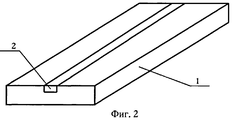
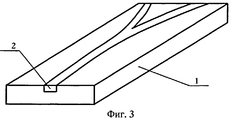
Сущность предлагаемого изобретения поясняется чертежами, где на фиг.1 изображен ИОЭ (вид с торца), состоящий из подложки 1 и оптического канального волновода 2; на фиг.2 - ИОЭ с прямоугольным оптическим канальным волноводом; на фиг.3 - ИОЭ с конфигураций оптического канального волновода в виде Y-ветвителя.The essence of the invention is illustrated by drawings, where figure 1 shows the IOE (end view), consisting of a
ИОЭ представляет собой подложку 1 и оптический канальный волновод 2. На поверхность подложки 1 наносят слой фоторезиста, после чего проводят экспонирование через фотошаблон (конфигурация фотошаблона может быть различной, например, как на фиг.2, представлена конфигурация Y-ветвителя), затем проявляют. Далее в образовавшиеся окна по конфигурации фотошаблона вводят водный раствор уксусной, щавелевой, соляной или серной кислот, по экспериментальным данным контакт поверхности подложки 1 необходимо осуществлять от нескольких до 10 секунд в зависимости от используемого раствора кислоты. Затем промывают до отсутствия кислой реакции и удаляют слой фоторезиста. На подложке 1 в точности по конфигурации фотошаблона возникает нанопористый слой, глубина которого не превышает 5-10 мкм. Пористость слоя составляет 20-25%. Распределение объема пор по радиусам таково, что в нем нет пор с диаметром более 7 нм. Далее подложку 1 помещают в концентрированный раствор соли цезия, рубидия, германия, олова или свинца, а после насыщения этими солями пор выщелоченного слоя подложку 1 извлекают из раствора, содержащего соли упомянутых металлов, и подвергают нагреванию при температуре 550°С в течение 40 минут, которое приводит к термическому разложению солей и взаимодействию образовавшихся окислов с каркасом пористого слоя, в результате образуются участки стекла с повышенным показателем преломления. Этот слой образовавшегося стекла в подложке 1 и есть оптический канальный волновод 2. Далее с торцов подложки 1 сполировывают слой, подверженный реакции с кислотой.The IOE is a
Подложка 1 представляет собой пластину ликвировавшего (отожженного при температуре 530°С в течение 72 часов) натрийборосиликатного стекла состава Na2O:В2О3:SiO2=7:23:70. Показатель преломления подложки 1 равен 1,51. Образованный оптический канальный волновод 2 имеет показатель преломления выше показателя преломления подложки 1, чтобы обеспечить условие волноводного распространения. Максимальная величина приращения показателя преломления Δn=0,011 и зависит от введенных солей.The
Таким образом, заявляемое техническое решение позволяет значительно упростить технологию изготовления ИОЭ. Использование в качестве подложки натрийборосиликатного стекла обеспечивает дешевизну конечного продукта - ИОЭ и интегрально-оптических устройств на их основе. Данная технология не требует для изготовления волновода проведения операций при высоких температурах, а следовательно, не требует дорогостоящего оборудования. Введение солей тяжелых металлов позволяет управлять параметрами получаемых оптических волноводов в зависимости от концентраций растворов, длительности контакта и показателя преломления. На базе таких ИОЭ можно создавать многофункциональные интегрально-оптические устройства, содержащие как пассивные, так и активные элементы.Thus, the claimed technical solution can significantly simplify the manufacturing technology of the IOE. The use of sodium borosilicate glass as a substrate ensures low cost of the final product - IOE and integrated optical devices based on them. This technology does not require operations at high temperatures for the manufacture of a waveguide, and therefore does not require expensive equipment. The introduction of salts of heavy metals allows you to control the parameters of the obtained optical waveguides depending on the concentration of the solutions, the duration of the contact and the refractive index. Based on such IOEs, it is possible to create multifunctional integrated optical devices containing both passive and active elements.
Claims (2)
Priority Applications (1)
| Application Number | Priority Date | Filing Date | Title |
|---|---|---|---|
| RU2009145607/28A RU2425402C1 (en) | 2009-12-08 | 2009-12-08 | Integrated optical element and method of making said element |
Applications Claiming Priority (1)
| Application Number | Priority Date | Filing Date | Title |
|---|---|---|---|
| RU2009145607/28A RU2425402C1 (en) | 2009-12-08 | 2009-12-08 | Integrated optical element and method of making said element |
Publications (1)
| Publication Number | Publication Date |
|---|---|
| RU2425402C1 true RU2425402C1 (en) | 2011-07-27 |
Family
ID=44753684
Family Applications (1)
| Application Number | Title | Priority Date | Filing Date |
|---|---|---|---|
| RU2009145607/28A RU2425402C1 (en) | 2009-12-08 | 2009-12-08 | Integrated optical element and method of making said element |
Country Status (1)
| Country | Link |
|---|---|
| RU (1) | RU2425402C1 (en) |
Cited By (1)
| Publication number | Priority date | Publication date | Assignee | Title |
|---|---|---|---|---|
| RU2524460C1 (en) * | 2013-02-14 | 2014-07-27 | Федеральное государственное бюджетное образовательное учреждение высшего профессионального образования "Кубанский государственный университет" (ФГБОУ ВПО "КубГУ") | Method of producing integrated optical circuit on glass substrate with horn-shaped waveguide |
-
2009
- 2009-12-08 RU RU2009145607/28A patent/RU2425402C1/en not_active IP Right Cessation
Cited By (1)
| Publication number | Priority date | Publication date | Assignee | Title |
|---|---|---|---|---|
| RU2524460C1 (en) * | 2013-02-14 | 2014-07-27 | Федеральное государственное бюджетное образовательное учреждение высшего профессионального образования "Кубанский государственный университет" (ФГБОУ ВПО "КубГУ") | Method of producing integrated optical circuit on glass substrate with horn-shaped waveguide |
Similar Documents
| Publication | Publication Date | Title |
|---|---|---|
| Izawa et al. | Optical waveguide formed by electrically induced migration of ions in glass plates | |
| US10670806B2 (en) | Method for preparing film micro-optical structure based on photolithography and chemomechanical polishing | |
| Guarino et al. | Electro–optically tunable microring resonators in lithium niobate | |
| US6185355B1 (en) | Process for making high yield, DC stable proton exchanged waveguide for active integrated optic devices | |
| Tervonen et al. | Ion-exchanged glass waveguide technology: a review | |
| US4400052A (en) | Method for manufacturing birefringent integrated optics devices | |
| KR970009093B1 (en) | Optical waveguide manufacturing method and product produced therefrom | |
| JPH04234005A (en) | Manufacture of lightguide tube by ion exchange method | |
| Righini et al. | Sol-gel glass waveguides | |
| RU2151412C1 (en) | Method for manufacturing of optical waveguide | |
| RU2425402C1 (en) | Integrated optical element and method of making said element | |
| Kapila et al. | Solid‐State film diffusion for the production of integrated optical waveguides | |
| Eguchi et al. | Fabrication of low-loss waveguides in BK-7 by ion exchange | |
| CN106291816A (en) | A kind of method improving glass based optical waveguide chip uniformity | |
| JP3898585B2 (en) | Method for manufacturing member with optical waveguide | |
| Elalamy et al. | Thermo-optical coefficients of sol–gel ZrO2 thin films | |
| US20110311180A1 (en) | Glassy Surface Smoothing Layer for Integrated Waveguide | |
| Jin et al. | Lithium–Niobate Channel Waveguide for the Realization of Long-Period Gratings | |
| Righini et al. | Integrated optical components fabricated by two-step ion-exchange | |
| JP2004037587A (en) | Optical modulator and method for manufacturing the same | |
| Grelin et al. | Study of Ag+/Na+ ion-exchange diffusion on germanate glasses: realization of single-mode waveguides at the wavelength of 1.55 μm | |
| Tong Ph. D et al. | Glass Waveguides | |
| Josse et al. | Planar and channel waveguides on fluoride glasses | |
| RU2594987C1 (en) | Integrated optical element | |
| JPS6385506A (en) | Manufacture of light waveguide for medium infrared spectrum |
Legal Events
| Date | Code | Title | Description |
|---|---|---|---|
| MM4A | The patent is invalid due to non-payment of fees |
Effective date: 20191209 |