RU2271069C2 - Method and circuit for synchronous data reception during high-speed data transfer from subscriber to central point in optical data transfer system - Google Patents
Method and circuit for synchronous data reception during high-speed data transfer from subscriber to central point in optical data transfer system Download PDFInfo
- Publication number
- RU2271069C2 RU2271069C2 RU2003136099/09A RU2003136099A RU2271069C2 RU 2271069 C2 RU2271069 C2 RU 2271069C2 RU 2003136099/09 A RU2003136099/09 A RU 2003136099/09A RU 2003136099 A RU2003136099 A RU 2003136099A RU 2271069 C2 RU2271069 C2 RU 2271069C2
- Authority
- RU
- Russia
- Prior art keywords
- data
- clock frequency
- block
- channels
- circuit
- Prior art date
Links
- 238000000034 method Methods 0.000 title claims abstract description 35
- 230000003287 optical effect Effects 0.000 title claims abstract description 12
- 230000001360 synchronised effect Effects 0.000 title claims description 48
- 230000005540 biological transmission Effects 0.000 claims abstract description 27
- 238000001514 detection method Methods 0.000 claims abstract description 24
- 238000006243 chemical reaction Methods 0.000 claims abstract description 17
- 238000005070 sampling Methods 0.000 claims description 42
- 230000006978 adaptation Effects 0.000 claims description 14
- 230000003044 adaptive effect Effects 0.000 claims description 5
- 239000013598 vector Substances 0.000 claims description 5
- 238000011084 recovery Methods 0.000 claims description 4
- 230000000694 effects Effects 0.000 abstract 1
- 239000000126 substance Substances 0.000 abstract 1
- 238000005516 engineering process Methods 0.000 description 6
- 101150085102 Clk3 gene Proteins 0.000 description 5
- BDEDPKFUFGCVCJ-UHFFFAOYSA-N 3,6-dihydroxy-8,8-dimethyl-1-oxo-3,4,7,9-tetrahydrocyclopenta[h]isochromene-5-carbaldehyde Chemical compound O=C1OC(O)CC(C(C=O)=C2O)=C1C1=C2CC(C)(C)C1 BDEDPKFUFGCVCJ-UHFFFAOYSA-N 0.000 description 2
- 238000010586 diagram Methods 0.000 description 2
- 101100328957 Caenorhabditis elegans clk-1 gene Proteins 0.000 description 1
- 101100113692 Caenorhabditis elegans clk-2 gene Proteins 0.000 description 1
- 238000009434 installation Methods 0.000 description 1
- 230000003068 static effect Effects 0.000 description 1
Images


Classifications
-
- H—ELECTRICITY
- H04—ELECTRIC COMMUNICATION TECHNIQUE
- H04L—TRANSMISSION OF DIGITAL INFORMATION, e.g. TELEGRAPHIC COMMUNICATION
- H04L7/00—Arrangements for synchronising receiver with transmitter
- H04L7/02—Speed or phase control by the received code signals, the signals containing no special synchronisation information
- H04L7/033—Speed or phase control by the received code signals, the signals containing no special synchronisation information using the transitions of the received signal to control the phase of the synchronising-signal-generating means, e.g. using a phase-locked loop
- H04L7/0337—Selecting between two or more discretely delayed clocks or selecting between two or more discretely delayed received code signals
- H04L7/0338—Selecting between two or more discretely delayed clocks or selecting between two or more discretely delayed received code signals the correction of the phase error being performed by a feed forward loop
-
- H—ELECTRICITY
- H04—ELECTRIC COMMUNICATION TECHNIQUE
- H04L—TRANSMISSION OF DIGITAL INFORMATION, e.g. TELEGRAPHIC COMMUNICATION
- H04L7/00—Arrangements for synchronising receiver with transmitter
- H04L7/04—Speed or phase control by synchronisation signals
Landscapes
- Engineering & Computer Science (AREA)
- Computer Networks & Wireless Communication (AREA)
- Signal Processing (AREA)
- Synchronisation In Digital Transmission Systems (AREA)
- Optical Communication System (AREA)
Abstract
Description
Область техники, к которой относится изобретениеFIELD OF THE INVENTION
Настоящее изобретение, в общем, относится к технологии оптической передачи данных, в частности к способу и схеме синхронного приема данных, передаваемых по оптической системе передачи данных от абонента на центральный узел в высокоскоростном пакетном режиме.The present invention, in General, relates to optical data transmission technology, in particular to a method and circuit for synchronously receiving data transmitted via an optical data transmission system from a subscriber to a central node in high-speed packet mode.
Уровень техникиState of the art
Для решения проблемы синхронизации при передаче данных от абонента на центральный узел в случае использования пассивной оптической сети с асинхронным режимом передачи (АРП (АТМ) (А-ПОС (A-PON)), при использовании технологии высокоскоростного множественного доступа с временным разделением каналов (МДВР (TDMA)), необходимо использовать специальную технологию и способ. Например, работа каждой ячейки, из которой осуществляют доступ к терминалу оптической линии (ТОЛ (OLT)) в асинхронном режиме передачи (АРП), должна быть приблизительно синхронизирована с ее диапазоном, но даже в этом случае существует некоторый, не равный целому числу бит интервал между ячейками, работающими в АРП. В этом случае для совмещения данных необходимо использовать синхронизацию битов и одновременно осуществлять синхронизацию байтов данных и ячеек. В настоящем изобретении эту проблему называют проблемой приема для высокоскоростной синхронизации битов. В качестве другого примера можно отметить, что поскольку данные, передаваемые из ячеек, работающих в АРП, от абонента на центральный узел, поступают через различные удаленные терминалы, и их передача производится в пакетном режиме, необходимо обеспечить индивидуальную синхронизацию для каждой ячейки.To solve the problem of synchronization when transferring data from a subscriber to a central node in the case of using a passive optical network with asynchronous transmission mode (ATM (ATM) (A-POS (A-PON)), using the technology of high-speed multiple access with time division multiplexing (TDMA) (TDMA)), it is necessary to use a special technology and method, for example, the operation of each cell from which the optical line terminal (TOL (OLT)) is accessed in asynchronous transmission mode (ATM) should be approximately synchronized on with its range, but even in this case there is some interval, not equal to an integer number of bits, between cells working in the ATM. In this case, to combine data, it is necessary to use bit synchronization and synchronize data bytes and cells simultaneously. In the present invention, this problem called the reception problem for high-speed synchronization of bits. As another example, it can be noted that since the data transmitted from the cells operating in the ATM from the subscriber to the central node comes through personal remote terminals, and the transmission is performed in batch mode, you must provide the individual timing for each cell.
Во время указанного выше синхронного приема для обеспечения максимальной устойчивости по времени тактовую частоту выборки на конце приема ТОЛ устанавливают по середине наблюдаемой структуры входных данных. При этом обычно используют способ индивидуальной установки, основанный на схеме фазовой синхронизации (СФС (PLL)). При использовании такой технологии вначале с помощью фазового детектора определяют фазы передних и задних фронтов импульсов последовательных данных, передаваемых в пакетном режиме от абонента на центральный узел, и тактовую частоту выборки для генерирования "восходящего" и "нисходящего" импульсов; затем эти два импульса передают в "насос загрузки", и затем выходное напряжение насоса загрузки используют для изменения частоты генератора, управляемого напряжением (ГУН (VCO)), для получения тактовой частоты с соответствующей фазой.During the above synchronous reception, to ensure maximum time stability, the sampling clock frequency at the end of TOL reception is set in the middle of the observed input data structure. In this case, an individual installation method is usually used, based on a phase synchronization scheme (SPS (PLL)). When using this technology, first, using the phase detector, the phases of the leading and trailing edges of the serial data pulses are determined, which are transmitted in batch mode from the subscriber to the central node, and the sampling clock frequency for generating “up” and “down” pulses; then these two pulses are transmitted to the “loading pump”, and then the output voltage of the loading pump is used to change the frequency of the voltage-controlled generator (VCO) to obtain the clock frequency with the corresponding phase.
Недостаток технологии СФС состоит в следующем. Во-первых, при использовании технологии СФС необходимо длительное время для разъединения, чтобы обеспечить стабильную синхронизацию по фазе, что не совместимо с характеристиками высокоскоростной передачи данных, передаваемых в пакетном режиме от абонента на центральный узел в системе А-ПОС. Во-вторых, трудно построить схему детектирования фазы для обеспечения детектирования фазы данных, передаваемых от абонента на центральный узел, в режиме высокоскоростной пакетной передачи, и тактовой частоты выборки. В-третьих, трудно получить небольшое значение статической погрешности фазы и динамической ошибки определения фазы между тактовой частотой выборки и последовательно поступающими данными, передаваемыми в высокоскоростном пакетном режиме от абонента на центральный узел; например, это касается времени задержки, времени синхронной задержки и нелинейных характеристик фазового детектора, так как в нем для обеспечения стабильности требуется обеспечить малую полосу пропускания петли обратной связи, но в этом случае схема не позволяет отслеживать высокочастотные шумы.The disadvantage of SPS technology is as follows. Firstly, when using SPS technology, it takes a long time for disconnection to ensure stable phase synchronization, which is not compatible with the characteristics of high-speed data transfer transmitted in batch mode from a subscriber to a central node in the A-POS system. Secondly, it is difficult to construct a phase detection circuit to ensure the phase detection of data transmitted from the subscriber to the central node in high-speed packet transmission mode and the sampling clock frequency. Thirdly, it is difficult to obtain a small value of the static phase error and the dynamic error of determining the phase between the clock sampling frequency and sequentially incoming data transmitted in high speed packet mode from the subscriber to the central node; for example, this concerns the delay time, the synchronous delay time, and the nonlinear characteristics of the phase detector, since it requires a small bandwidth of the feedback loop to ensure stability, but in this case the circuit does not allow tracking of high-frequency noise.
Другой способ позиционирования, который используют более часто, состоит в использовании выборки с избыточностью, когда тактовая частота имеет четыре фазы для данных, передаваемых по каналу от абонента на центральный узел, в режиме высокоскоростной последовательной пакетной передачи. На дальнем конце в передаваемую головную часть данных, передаваемых в режиме высокоскоростной последовательной пакетной передачи от абонента на центральный узел, ячейки, работающей в АРП, добавляют специальный заголовок (преамбулу); при этом на конце автоматического коммутатора каналов, если при использовании некоторой тактовой частоты получают выборку правильного кода заголовка, считается, что фаза тактовой частоты удовлетворяет требованиям по фазе, и эту тактовую частоту выбирают в качестве синхронной тактовой частоты, и затем выполняют выборку битовых данных, преобразование данных в байтовую форму и реверсирование ячейки, и т.д.Another positioning method, which is used more often, is to use redundancy sampling when the clock frequency has four phases for the data transmitted over the channel from the subscriber to the central node in high-speed sequential packet transmission mode. At the far end, a special header (preamble) is added to the transmitted head part of the data transmitted in the high-speed sequential packet transmission mode from the subscriber to the central node of the cell operating in the ATM; at the end of the automatic channel switcher, if a certain header code is sampled using a certain clock frequency, it is considered that the phase of the clock frequency satisfies the phase requirements, and this clock frequency is selected as the synchronous clock frequency, and then bit data is sampled, conversion data in byte form and cell reversal, etc.
Недостаток этого способа состоит в следующем. Во-первых, выбранная тактовая частота не всегда устанавливается в середине наблюдаемой структуры данных, так что допуски по времени могут быть очень незначительными. Во-вторых, при высокой скорости передачи данных трудно удовлетворить требования, предъявляемые к системе. В-третьих, трудно обеспечить точное отслеживание фазового шума системы.The disadvantage of this method is as follows. First, the selected clock frequency is not always set in the middle of the observed data structure, so the time tolerances can be very small. Secondly, at high data rates it is difficult to satisfy the requirements of the system. Third, it is difficult to accurately track the phase noise of a system.
Сущность изобретенияSUMMARY OF THE INVENTION
Настоящее изобретение направлено на способ и схему синхронного приема высокоскоростных данных, передаваемых от абонента на центральный узел, предназначенные для решения проблем, указанных выше, с использованием простого устройства и выполнения.The present invention is directed to a method and circuit for the synchronous reception of high-speed data transmitted from a subscriber to a central node, designed to solve the problems indicated above using a simple device and execution.
Цель настоящего изобретения достигается с использованием следующего технического решения: способ синхронного приема при высокоскоростной передаче данных от абонента на центральный узел в системе оптической передачи данных, при котором используют многофазную тактовую частоту с различными фазами для синхронного приема высокоскоростных битов, при этом способ содержит:The purpose of the present invention is achieved using the following technical solution: a method of synchronous reception during high-speed data transmission from a subscriber to a central node in an optical data transmission system, in which a multiphase clock frequency with different phases is used to synchronously receive high-speed bits, the method comprising:
А. использование тактовой частоты с Х различными фазами для обеспечения выборки с избыточностью высокоскоростных последовательных данных, передаваемых в пакетном режиме от абонента на центральный узел, для получения данных, передаваемых по Х каналам, адаптацию данных, передаваемых по Х каналам, к локальной тактовой частоте, где Х представляет собой целое положительное число;A. the use of a clock frequency with X different phases to ensure redundancy of high-speed serial data transmitted in a batch mode from a subscriber to a central node, to receive data transmitted over X channels, adaptation of data transmitted over X channels to a local clock frequency, where X is a positive integer;
В. детектирование кодов заголовков данных, передаваемых по Х каналам, адаптированных к локальной тактовой частоте, определение корректно принятых данных;B. detection of codes of data headers transmitted over X channels adapted to the local clock frequency, determination of correctly received data;
С. выбор корректных данных, выборка которых была проведена с использованием тактовой частоты, установленной в середине наблюдаемой структуры корректных данных, выполнение последовательно-параллельного преобразования, а также синхронизацию байтов и ячейки для выбранных корректных данных.C. the selection of the correct data, the selection of which was carried out using the clock frequency set in the middle of the observed structure of the correct data, the execution of serial-parallel conversion, as well as the synchronization of bytes and cells for the selected correct data.
Указанные тактовые частоты с Х различными фазами представляют собой тактовые частоты с 8 или 16 различными фазами, и разность фаз для каждых двух последующих тактовых частот равна 1/Х периода тактовой частоты.The indicated clock frequencies with X different phases are clock frequencies with 8 or 16 different phases, and the phase difference for each two subsequent clock frequencies is equal to 1 / X of the clock frequency period.
Этап А дополнительно содержит: генерирование с помощью генератора тактовой частоты Х тактовых частот с равной разностью фаз; выполнение с помощью Х схем выборки, соответствующих указанной Х-фазной тактовой частоте, выборки с избыточностью высокоскоростных последовательных данных, передаваемых в пакетном режиме от абонента на центральный узел, и получение данных, передаваемых по Х каналам; выполнение с помощью Х адаптирующих каскадов, соответствующих Х схемам выборки, адаптации указанных данных, передаваемых по Х каналам, к локальной тактовой частоте; выполнение сдвига и синхронизации указанных адаптированных данных, передаваемых по Х каналам, с помощью Х каскадов сдвига, соответствующих Х адаптирующим каскадам.Step A further comprises: generating, using a clock generator, X clock frequencies with an equal phase difference; performing using X sampling schemes corresponding to the indicated X-phase clock frequency, redundant sampling of high-speed serial data transmitted in batch mode from the subscriber to the central node, and receiving data transmitted on X channels; execution using X adaptive cascades corresponding to X sampling schemes, adaptation of the specified data transmitted over X channels to the local clock frequency; performing a shift and synchronization of said adapted data transmitted over X channels using X shift cascades corresponding to X adaptation cascades.
Каждая из указанных Х схем выборки включает трехкаскадные регистры, соединенные последовательно, которые производят сдвиг данных с указанной Х-фазной тактовой частотой, для устранения нестабильности принимаемого сигнала.Each of the indicated X sampling circuits includes three-stage registers connected in series, which shift data at the indicated X-phase clock frequency, to eliminate the instability of the received signal.
Адаптацию данных, передаваемых по Х каналам, к указанной локальной тактовой частоте выполняют с помощью соответствующих Х адаптирующих каскадов; адаптацию выполняют следующим образом: выходные данные регистра, управляемого с помощью тактовой частоты, передают в качестве входных данных в регистр, управляемый другой тактовой частотой и, в конце концов, передают в регистр, управляемый указанной локальной тактовой частотой.Adaptation of data transmitted over X channels to a specified local clock frequency is performed using the corresponding X adaptive stages; adaptation is performed as follows: the output of a register controlled by a clock frequency is transmitted as input to a register controlled by a different clock frequency and, finally, transferred to a register controlled by a specified local clock frequency.
Сдвиг указанных адаптированных данных, выполняемый с помощью указанных каскадов сдвига, по указанной локальной тактовой частоте, выполняют с помощью последовательно соединенных регистров, содержащих 8+1 каскадов.The shift of the specified adapted data, performed using the indicated cascades of shift, at the specified local clock frequency, is performed using series-connected registers containing 8 + 1 cascades.
Этап В дополнительно содержит: сравнение указанных адаптированных данных с кодами заголовков и определение данных с кодом заголовка, детектированным в качестве корректных данных; выполнение детектирования полярности и измерение переднего фронта и заднего фронта указанных корректных данных для замены данных, передаваемых по этому каналу.Step B further comprises: comparing said adapted data with header codes and determining data with a header code detected as valid data; performing polarity detection and measuring the leading edge and trailing edge of the specified correct data to replace the data transmitted on this channel.
Во время выполнения сравнения адаптированных данных, содержащих коды заголовков, в случае, когда все биты адаптированных данных идентичны коду заголовка, или только один из битов не идентичен коду заголовка, принимают решение, что код заголовка был детектирован, и данные с этим кодом заголовка представляют собой корректные данные.During the comparison of the adapted data containing the header codes, in the case when all bits of the adapted data are identical to the header code, or only one of the bits is not identical to the header code, it is decided that the header code has been detected, and the data with this header code is correct data.
Указанное детектирование полярности дополнительно включает: сравнение бит за битом корректных данных, содержащих указанный код заголовка, для установки исходных векторов индексов hit1-hit8, и в случае, когда биты различаются, соответствующий индекс (hit) устанавливают равным "0", а когда они идентичны, соответствующий индекс устанавливают равным "1"; выполнение операции исключающее ИЛИ для двух последовательных индексов и помещение результата в флаг - Flag; при этом биты младшей значащей "1" и старшей значащей "1" представляют, соответственно, передний фронт и задний фронт указанных корректных данных.The specified polarity detection further includes: comparing bit by bit the correct data containing the specified header code to set the original index vectors hit1-hit8, and when the bits are different, the corresponding index (hit) is set to "0", and when they are identical , the corresponding index is set equal to "1"; execution of an exclusive OR operation for two consecutive indices and putting the result in a flag - Flag; while the bits of the least significant "1" and the most significant "1" represent, respectively, the leading edge and falling edge of the specified valid data.
Этап С дополнительно включает: определение указанного положения "а" бита младшей значащей " 1" и положения "b" бита старшей значащей "1" в указанном флаге с помощью логической схемы выбора и выбор корректных данных, выборка которых была проведена на тактовой частоте с номером (а+b)/2 фазы, для выполнения последовательно-параллельного преобразования и синхронизации ячейки.Step C additionally includes: determining the indicated position “a” of the least significant bit “1” and the position “b” of the highest significant bit “1” in the indicated flag using the selection logic and selecting the correct data that were sampled at the clock frequency with the number (a + b) / 2 phases, for performing series-parallel conversion and cell synchronization.
Этот этап дополнительно включает деление указанной локальной тактовой частоты для получения тактовой частоты восстановления, используемой для последовательно-параллельного преобразования, причем указанную тактовую частоту восстановления также передают через указанную схему синхронного приема вместе с синхронизированными передаваемыми данными байта и ячейки.This step further includes dividing said local clock frequency to obtain a clock clock used for serial-parallel conversion, wherein said clock clock is also transmitted through said synchronous reception circuit along with synchronized transmitted byte and cell data.
Цель настоящего изобретения также может быть достигнута благодаря использованию схемы: она отличается тем, что схема синхронного приема при высокоскоростной передаче данных от абонента на центральный узел в системе оптической передачи данных, включающей:The purpose of the present invention can also be achieved through the use of the scheme: it is characterized in that the synchronous reception scheme for high-speed data transmission from a subscriber to a central node in an optical data transmission system, including:
блок схемы генерирования тактовой частоты, предназначенный для получения X-фазной тактовой частоты, блок схемы выборки, предназначенный для высокоскоростной последовательной передачи данных в пакетном режиме от абонента на центральный узел по Х каналам, блок схемы детектирования кодов заголовков, предназначенный для детектирования кодов заголовков данных, передаваемых по Х каналам, блок логической схемы выбора и блок синхронизации байта и ячейки, который состоит из блока схемы выбора данных, передаваемых по Х каналам, блока схемы выбора синхронного сигнала и блока схемы последовательно-параллельного преобразования;a clock frequency generating circuit block for obtaining an X-phase clock frequency, a sampling circuit block for high-speed serial data transmission in batch mode from a subscriber to a central node via X channels, a header code detection circuit block for detecting data header codes, transmitted over X channels, a block of the logic selection circuit and a synchronization block of a byte and a cell, which consists of a block of a circuit for selecting data transmitted over X channels, a block of a selection circuit a synchronous signal and a block scheme a serial to parallel conversion;
указанная Х-фазная тактовая частота с различными фазами, генерируемая с помощью указанного блока генерирования тактовой частоты, поступает в указанный блок схемы выборки данных, передаваемых по Х каналам, соответственно;the specified X-phase clock frequency with different phases generated using the specified block generating a clock frequency, is supplied to the specified block of the sampling circuit of data transmitted over X channels, respectively;
и указанный блок схемы выборки соединен с указанным блоком схемы детектирования кода заголовка данных, передаваемых по Х каналам, и указанным блоком схемы выбора данных, передаваемых по Х каналам, указанного блока синхронизации байта и ячейки, соответственно;and said block of a sampling circuit is connected to said block of a circuit for detecting a header code of data transmitted over X channels and said block of a circuit for selecting data transmitted over X channels of said byte and cell synchronization block, respectively;
указанный блок схемы детектирования кода заголовка соединен с указанным блоком логической схемы выбора и с указанным блоком выбора синхронного сигнала, указанного блока синхронизации байта и ячейки, соответственно;said block of the header code detection circuitry is connected to said block of a logic selection circuit and to said block of selecting a synchronous signal, said synchronization block of a byte and a cell, respectively;
указанный блок логической схемы выбора соединен с указанным блоком схемы выбора синхронного сигнала и блоком схемы выбора данных, передаваемых по Х каналам, указанного блока синхронизации байта и ячейки, соответственно;said block of a logic selection circuit is connected to said block of a synchronous signal selection circuit and a block of a circuit for selecting data transmitted over X channels of said byte and cell synchronization block, respectively;
указанный блок схемы выбора синхронного сигнала и указанный блок схемы выбора данных, передаваемых по Х каналам, указанного блока синхронизации байта и ячейки соединены с указанным блоком последовательно-параллельного преобразования, соответственно;said block of a circuit for selecting a synchronous signal and said block of a circuit for selecting data transmitted over X channels of said byte block and cells are connected to said block of serial-parallel conversion, respectively;
указанная локальная тактовая частота поступает в указанный блок схемы выборки и в указанный блок детектирования кода заголовка данных, передаваемых по Х каналам, соответственно.the specified local clock frequency is supplied to the indicated block of the sampling circuit and to the indicated block for detecting the code of the header of the data transmitted over X channels, respectively.
Устройство также содержит схему деления указанной локальной тактовой частоты, которая непосредственно генерирует тактовую частоту восстановления, используемую для последовательно-параллельного преобразования, и указанная тактовая частота восстановления поступает на выход указанной схемы синхронного приема вместе с данными синхронизированного байта и данными ячейки.The device also comprises a division circuit of the indicated local clock frequency, which directly generates a clock frequency of recovery used for serial-parallel conversion, and the indicated clock frequency of restoration is supplied to the output of the specified synchronous reception circuit along with the synchronized byte data and cell data.
Каждый указанный выше канал схемы выборки состоит из последовательно включенных каскадов выборки, которые используются для устранения подстабильных состояний адаптирующего каскада, который выполняет адаптацию указанных данных выборки с указанной локальной тактовой частотой, и каскада сдвига, который осуществляет синхронизацию данных.Each channel of the sampling circuit indicated above consists of sequentially connected sampling cascades, which are used to eliminate the stable states of the adaptation cascade, which performs adaptation of the indicated sample data with the indicated local clock frequency, and a shift cascade, which synchronizes the data.
Указанный блок логических схем выбора включает соединенные генератор временной последовательности, регистр первого флага, регистр второго флага, первую схему декодирования, вторую схему декодирования, первый регистр, второй регистр, сумматор и селектор;The indicated block of logic selection circuitry includes a connected time sequence generator, a first flag register, a second flag register, a first decoding scheme, a second decoding scheme, a first register, a second register, an adder and a selector;
указанный последовательный генератор соединен с первым регистром флага, вторым регистром флага, первым регистром, вторым регистром и указанным селектором, соответственно;said serial generator is connected to a first flag register, a second flag register, a first register, a second register, and said selector, respectively;
указанный первый регистр флага, первая схема декодирования и первый регистр соединены последовательно и затем соединены с одним из входов указанного сумматора;said first flag register, a first decoding circuit, and a first register are connected in series and then connected to one of the inputs of said adder;
указанный второй регистр флага, вторая схема декодирования и второй регистр соединены последовательно и затем подключены к другому входу указанного сумматора;said second flag register, a second decoding circuit, and a second register are connected in series and then connected to another input of said adder;
выход указанного сумматора соединен с указанным селектором; и в первый регистр флага, второй регистр флага, первый регистр и второй регистр поступает локальная тактовая частота.the output of the specified adder is connected to the specified selector; and in the first register of the flag, the second register of the flag, the first register and the second register the local clock frequency.
Указанный блок генерирования тактовой частоты с Х фазами выполнен по схеме фазовой синхронизации (СФС) или по схеме цифровой синхронизации (СЦС (DLL)).The specified block generating a clock frequency with X phases is made according to the phase synchronization scheme (SFS) or according to the digital synchronization scheme (SCS (DLL)).
Способ и схема синхронного приема, в соответствии с настоящим изобретением, при высокоскоростной передаче данных от абонента на центральный узел в системе оптической передачи данных предложены для решения недостатков существующего технического решения, и представляют собой способ и схему приема с высокоскоростной битовой синхронизацией. Способ содержит следующие этапы: вначале выполняют выборку с избыточностью высокоскоростных данных, передаваемых в пакетном режиме от абонента на центральный узел, с помощью многофазной тактовой частоты (содержащей, например, 8-16 фаз) и адаптацию данных, для которых была проведена выборка с избыточностью, к локальной тактовой частоте, затем производят детектирование кода заголовка (например, в виде кода Бэйкера (baker code)), на основании результата детектирования затем выбирают данные, выборка которых была проведена с использованием тактовой частоты, установленной в середине наблюдаемой структуры данных, в качестве корректных данных для выполнения последовательно-параллельного преобразования, синхронизации байта и ячейки.The method and scheme for synchronous reception in accordance with the present invention, when high-speed data transmission from a subscriber to a central node in an optical data transmission system, are proposed to solve the shortcomings of the existing technical solution, and are a reception method and scheme with high-speed bit synchronization. The method comprises the following steps: first, redundancy is performed for high-speed data transmitted in a batch mode from a subscriber to a central node using a multiphase clock frequency (containing, for example, 8-16 phases) and adaptation of data for which redundancy was performed, to the local clock frequency, then the header code is detected (for example, in the form of a Baker code), based on the detection result, then the data that was sampled using the clock is selected the frequency set in the middle of the observed data structure as valid data for performing serial-parallel conversion, byte and cell synchronization.
Способ и схема синхронного приема, в соответствии с настоящим изобретением, при высокоскоростной передаче данных от абонента на центральный узел в системе оптической передачи данных, представляют собой способ и схему приема с высокоскоростной битовой синхронизацией. В этом способе используют многофазную тактовую частоту для выполнения выборки с избыточностью данных и адаптации данных, для которых была проведена выборка, к локальной тактовой частоте. В способе используют схему детектирования полярности для упрощения последующих схем, и используют логическую схему выбора для выбора данных, выборка которых была проведена с использованием тактовой частоты, установленной в середине наблюдаемой структуры. В способе используют добавление кода Бэйкера в качестве кода заголовка для высокоскоростной последовательной пакетной передачи данных от абонента на центральный узел. Настоящее изобретение направлено на выбор данных, а не на выбор тактовой частоты, и в нем используют высокую тактовую частоту с делением частоты для использования ее в качестве тактовой частоты байтов.The method and scheme for synchronous reception, in accordance with the present invention, when high-speed data transmission from a subscriber to a central node in an optical data transmission system, is a method and a reception scheme with high-speed bit synchronization. In this method, a multiphase clock frequency is used to sample with data redundancy and to adapt the data for which the sample was taken to the local clock frequency. The method uses a polarity detection circuit to simplify subsequent circuits, and uses a selection logic circuit to select data sampled using a clock frequency set in the middle of the observed structure. The method uses the addition of a Baker code as a header code for high-speed sequential packet data from a subscriber to a central node. The present invention is directed to the selection of data, not the choice of clock frequency, and it uses a high clock frequency with frequency division to use it as the clock frequency of bytes.
Сравнение со способом выборки по четырехфазной тактовой частоте для выполнения выборки с избыточностью при пакетной передаче данных от абонента на центральный узел, способ и схема в соответствии с настоящим изобретением, имеют следующие преимущества: использование большего количества различных фаз тактовой частоты позволяет обеспечить выборку с избыточностью, так, что обеспечивается большая степень детализации выборки, и это позволяет эффективно отслеживать фазовую ошибку системы; это позволяет надежно и точно выбирать тактовую частоту в середине наблюдаемой структуры принимаемых данных, так что в схеме обеспечивается максимальный допуск по времени; в схеме используют режим магистральной передачи данных без обратной связи, благодаря чему расчетная скорость передачи данных в схеме может быть существенно увеличена при удовлетворении условий битовой синхронизации при высокоскоростной передаче данных; схема выполняет обработку после синхронизации принятых данных с локальной тактовой частотой, так что схема может быть выполнена более просто, и в ней отсутствует неустойчивость фазы, в ней не требуется использовать регистры FIFO (регистры для организации очереди типа "первым пришел - первым обслуживается"), в ней легко осуществляется последовательное синхронное управление; схема позволяет непосредственно генерировать высокоскоростную тактовую частоту с делением частоты, так, что в ней отсутствуют шумы переключения тактовой частоты.Comparison with the four-phase clock sampling method for performing redundancy sampling during packet data transmission from the subscriber to the central node, the method and circuit in accordance with the present invention have the following advantages: using more different phases of the clock frequency allows redundant sampling, so that provides a large degree of detail of the sample, and this allows you to effectively track the phase error of the system; this allows you to reliably and accurately select the clock frequency in the middle of the observed structure of the received data, so that the maximum time tolerance is provided in the circuit; the scheme uses a backbone data transmission mode, which allows the calculated data transfer rate in the circuit to be significantly increased if the conditions for bit synchronization are met during high-speed data transmission; the circuit performs processing after synchronization of the received data with a local clock frequency, so that the circuit can be performed more simply, and there is no phase instability, it does not require FIFO registers (registers for queuing like “first-come-first-served”), sequential synchronous control is easily carried out in it; The circuit allows direct generation of a high-speed clock frequency with frequency division, so that there are no clock switching noise.
Краткое описание чертежейBrief Description of the Drawings
На фигуре 1 представлен принцип проведения выборки данных, передаваемых от абонента на центральный узел при использовании восьмифазной тактовой частоты.The figure 1 shows the principle of sampling data transmitted from the subscriber to the central node when using the eight-phase clock frequency.
На фигуре 2 показана схема приема при использовании восьмифазной тактовой частоты для обеспечения высокоскоростной битовой синхронизации.2 shows a reception pattern using an eight-phase clock to provide high speed bit synchronization.
На фигуре 3 показана схема одной фазы схемы выборки блока выборки данных, передаваемых от абонента на центральный узел, по фиг.2.Figure 3 shows a diagram of one phase of a sampling scheme of a block of sampling data transmitted from a subscriber to a central node, according to figure 2.
На фигуре 4 представлена схема детектирования полярности для блока схемы детектирования кода заголовка (кода Бэйкера) по фиг.2.FIG. 4 shows a polarity detection circuit for a block of a header code detection circuit (Baker code) of FIG. 2.
На фигуре 5 изображена схема логической схемы выбора.The figure 5 shows a diagram of the logic of the selection.
Осуществление изобретенияThe implementation of the invention
Настоящее изобретение будет более подробно описано ниже со ссылкой на чертежи, на которыхThe present invention will be described in more detail below with reference to the drawings, in which
на фигуре 1 представлен принцип выполнения выборки при высокоскоростной последовательной пакетной передаче данных от абонента на центральный узел при использовании восьмифазных тактовых частот, имеющих различные фазы. С использованием восьмифазных тактовых частот (Clk0-Clk7) с различными фазами выполняют выборку с избыточностью высокоскоростных последовательных данных, передаваемых в пакетном режиме от абонента на центральный узел; если при использовании всех восьмифазных тактовых частот Clk0-Clk7 были получены корректные данные выборки, в качестве принятых данных обычно используют данные, выборка которых была проведена с помощью тактовых частот Clk3 или Clk4, которые находятся в середине наблюдаемой структуры высокоскоростных последовательных данных, передаваемых в пакетном режиме, от абонента на центральный узел.the figure 1 shows the principle of sampling in high-speed sequential packet data from a subscriber to a central node using eight-phase clock frequencies having different phases. Using eight-phase clock frequencies (Clk0-Clk7) with different phases, redundancy of high-speed serial data is transmitted, transmitted in batch mode from the subscriber to the central node; if, using all Clk0-Clk7 eight-phase clock frequencies, the correct sample data was received, the received data is usually data that was sampled using the Clk3 or Clk4 clock frequencies, which are in the middle of the observed structure of high-speed serial data transmitted in batch mode , from the subscriber to the central site.
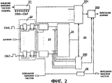
На фигуре 2 представлен основной принцип работы способа и принципиальная структура схемы. Она включает: блок 21 генерирования многофазной (восьмифазной) тактовой частоты, блок 22 схемы выборки высокоскоростных последовательных данных, передаваемых в пакетном режиме от абонента на центральный узел, блок 23 схемы детектирования кода Бэйкера (одного из кодов заголовка), блок 24 логической схемы выбора и блок 25 синхронизации байта ячейки, которые соединены с блоком 251 схемы выбора многоканальных (с восьмиканальных данных), блок 252 схемы выбора синхронного сигнала, и последовательно-параллельный преобразователь 253. Кроме того, схема содержит схему 26 деления тактовой частоты, коэффициент деления которой зависит от количества параллельных битов последовательно-параллельного преобразователя 253.The figure 2 presents the basic principle of the method and the basic structure of the circuit. It includes: a multiphase (eight-phase) clock
Блок 21 схемы генерирования многофазной тактовой частоты генерирует тактовые частоты, количество которых равно требуемому количеству фаз, и частота которых равна скорости передачи битов данных, передаваемых от абонента на центральный узел, и которые имеют равные разности фаз. Например, при скорости передачи высокоскоростных последовательных данных, передаваемых в пакетном режиме от абонента на центральный узел, равной 155 Мбит/с, и при внешней тактовой частоте, равной 155 МГц, генерируются восьмифазные тактовые частоты с частотой 155 МГц, и с равной разностью фаз, при этом период тактовой частоты равен 6,4 нс, и разность фаз между каждыми двумя последовательными тактовыми частотами составляет 1/8 внешнего периода тактовой частоты, то есть, 0,8 нс. Схема 21 многофазной тактовой частоты может быть построена с использованием обычного принципа фазовой синхронизации (СФС) или цифровой синхронизации (СЦС). Восемь тактовых частот Clk0-Clk7 поступают на схему 22 выборки высокоскоростных последовательных данных, передаваемых в пакетном режиме от абонента, на центральный узел.
Блок 22 схемы выборки высокоскоростных последовательных данных, передаваемых в пакетном режиме от абонента на центральный узел, состоит из с восьмиканальной схемы выборки, в которой восьмифазная тактовая частота Clk0-Clk7 используется для выполнения выборки с избыточностью высокоскоростных последовательных данных, передаваемых в пакетном режиме от абонента на центральный узел, для получения последовательных данных, передаваемых по восьми каналам, затем полученные данные адаптируют к локальной тактовой частоте, равной 155 МГц, с помощью преобразователя для последующей обработки.
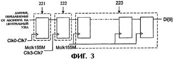
На фигуре 3 показан один канал (одна фаза) схемы 22 выборки, которая содержит три каскада, показанные тремя блоками, представленными пунктирными линиями.Figure 3 shows one channel (one phase) of a
Первый каскад представляет собой каскад 221 выборки, который выполняет выборку с избыточностью в режиме сдвига высокоскоростных последовательных данных, передаваемых в пакетном режиме от абонента на центральный узел, одной из восьми фазных тактовых частот Clk0-Clk7, и получает данные, соответствующие используемой тактовой частоте. Первый каскад может быть выполнен в виде трех последовательно соединенных каскадов регистров, что необходимо для устранения подстабильного состояния и нестабильности принимаемого сигнала.The first stage is a
Второй каскад представляет собой адаптирующий каскад 222, который используют для адаптации выбранных данных с избыточностью по отношению к основной тактовой частоте или к указанной локальной тактовой частоте (Mclk155 МГц) через частоты Clk3, Clk4, Clk5, Clk6 и Clk7 или непосредственно.The second stage is an
Адаптацию к основной тактовой частоте выполняют с использованием следующих взаимозависимостей, в которых выходные данные регистра, управляемые с помощью тактовой частоты, находящейся слева от стрелки →, передают на вход данных регистра, управляемого тактовой частотой, находящейся справа от стрелки.Adaptation to the main clock frequency is performed using the following interdependencies, in which the register output controlled by the clock located to the left of the arrow → is transferred to the register data input controlled by the clock located to the right of the arrow.
Clk0→Clk4→Mclk155M→Mclk155M;Clk0 → Clk4 → Mclk155M → Mclk155M;
Clk1→Clk5→Mclk155M→Mclk155M;Clk1 → Clk5 → Mclk155M → Mclk155M;
Clk2→Clk6→Clk3→Mclk155M;Clk2 → Clk6 → Clk3 → Mclk155M;
Clk3→Clk7→Clk4→Mclk155M;Clk3 → Clk7 → Clk4 → Mclk155M;
Clk4→Mclk155M→Mclk155M;Clk4 → Mclk155M → Mclk155M;
Clk5→Mclk155M→Mclk155M;Clk5 → Mclk155M → Mclk155M;
Clk6→Clk3→Mclk155M;Clk6 → Clk3 → Mclk155M;
Clk7→Clk4→Mclk155M.Clk7 → Clk4 → Mclk155M.
Из вышеприведенных взаимозависимостей можно видеть, что данные, синхронизированные с использованием восьмифазной тактовой частоты, в конце концов, получаются адаптированными к основной тактовой частоте или к локальной тактовой частоте (Mclk155 МГц).From the above interdependencies, it can be seen that data synchronized using an eight-phase clock frequency is ultimately adapted to the main clock frequency or to the local clock frequency (Mclk155 MHz).
Третий каскад представляет собой каскад 223 сдвига, который используется для синхронизации выходных данных адаптирующих каскадов 222. Выходные данные каждого канала были адаптированы к основной тактовой частоте, соответственно, и каждая из них с различной фазой тактовой частоты. Каскад 223 сдвига и регистр сдвига состоят из девяти включенных последовательно каскадных регистров. Восемь каскадов 223 сдвига передают 8 младших значащих битов последовательных данных в блок 23 схемы детектирования кода заголовка (кода Бэйкера), соответственно, и затем передают старший значащий бит (MSB) в блок 251 схемы выбора данных, соответственно, для выбора данных, как показано на фиг.2.The third stage is a
Схема 23 детектирования кода заголовка (кода Бэйкера) также включает восемь схем детектирования кода Бэйкера, которые выполняют, соответственно, детектирование кода заголовка для 8 младших значащих битов последовательных данных, поступающих на выход восьми каскадов 223 сдвига, для определения наличия корректных данных в восьми каналах. Каждая схема детектирования кода Бэйкера состоит из схем сравнения кодов Бэйкера и схемы детектирования полярности.The header code (Baker code)
На фигуре 4 представлен принцип работы схемы детектирования кода Бэйкера. Схема сравнения кода Бэйкера выполняет сравнение поступающих данных с кодом Бэйкера "11100101". На фиг.4 стрелки под не заштрихованной областью показывают результат процедуры сравнения; когда бит данных идентичен соответствующему биту кода Бэйкера, индекс исходного вектора устанавливают в "1", в противном случае в "0". Как показано на фиг.4, индексы hit1 и hit8 равны "0", и все индексы hit2-hit7 равны "1" (шесть "1"). В ходе сравнения, когда все биты равны, или только один бит не равен коду Бэйкера, определяется, что код Бэйкера был детектирован. Сравнение продолжается непрерывно по индексам hit8, hit1, hit2...hit7, hit8... и так далее.The figure 4 presents the principle of operation of the detection circuit of the Baker code. The Baker code comparison circuit compares the incoming data with the Baker code "11100101". In figure 4, the arrows under the unshaded area indicate the result of the comparison procedure; when the data bit is identical to the corresponding Baker code bit, the index of the source vector is set to "1", otherwise to "0". As shown in FIG. 4, the indices hit1 and hit8 are “0”, and all indices hit2-hit7 are “1” (six “1”). In the comparison, when all the bits are equal, or only one bit is not equal to the Baker code, it is determined that the Baker code has been detected. Comparison continues continuously at indices hit8, hit1, hit2 ... hit7, hit8 ... and so on.
Схему детектирования полярности используют для детектирования переднего фронта и заднего фронта высокоскоростных последовательных данных, передаваемых в пакетном режиме от абонента на центральный узел, и результат, который используют для замены данных выборки, передают в последующие схемы для дальнейшей обработки; таким образом, уменьшается объем вычислений, и упрощается дальнейшая обработка; поэтому вся схема позволяет выполнять обработку данных, передаваемых по восьми каналам, при тактовой частоте 155 МГц. В устройстве используют восемь логических элементов исключающее ИЛИ, которые выполняют логическую операцию исключающее ИЛИ для двух последовательных результатов сравнения кода Бэйкера. На фиг.4 - результат сравнения "01000001" последовательно записывают в восьмибитовый флаг, который в данном примере содержит "0" в младшем значащем бите и "1" в старшем значащем бите.The polarity detection circuit is used to detect the leading edge and trailing edge of high-speed serial data transmitted in batch mode from the subscriber to the central node, and the result, which is used to replace the sample data, is transmitted to subsequent circuits for further processing; thus, the amount of computation is reduced, and further processing is simplified; therefore, the entire circuit allows the processing of data transmitted over eight channels at a clock frequency of 155 MHz. The device uses eight exclusive OR logical elements that perform an exclusive OR logical operation for two consecutive Baker code comparison results. 4, the comparison result “01000001” is sequentially recorded in an eight-bit flag, which in this example contains “0” in the least significant bit and “1” in the most significant bit.
Как показано на фиг.4, данные флага содержат только два бита, равных "1", которые заменяют шесть битов, равных "1", исходного вектора индексов, и это упрощает последующие схемы.As shown in FIG. 4, the flag data contains only two bits equal to “1”, which replace six bits equal to “1” of the original index vector, and this simplifies the following schemes.
Логическая схема 24 выбора выполняет обработку наблюдаемой структуры данных размером 8×8 битов, поступающих со схемы 23 детектирования кода Бэйкера, для определения какая из фазных тактовых частот восьмифазных тактовых частот расположена в середине наблюдаемой структуры данных.The
Как показано на фиг.5, логическая схема 24 выбора содержит генератор 241 временной последовательности, флаг А (первый флаг) 242, состоящий из логических схем регистра, флаг В (второй флаг) 243, состоящий из логических схем регистра, логическую схему А 244 декодирования (первая логическая схема декодирования), логическую схему В 245 декодирования В (вторая схема декодирования), регистр А (первый регистр) 246, регистр В (второй регистр) 247, сумматор 248 (+), и селектор (SEL) 249, состоящий из логических схем регистра. Блок 24 логической схемы выбора определяет положение "а" первой "1" в флаге и положение "b" второй "1" в флаге для вычисления номера (а+b)/2 фазы частоты, которая расположена в середине наблюдаемой структуры корректных данных, с помощью сумматора 248 и селектора 249. Как показано на фиг.4, положение "а" первой "1" в флаге равно 2, и положение "b" второй "1" равно 8, так что (2+8)/2=5, и частота Clk5 будет расположена в середине наблюдаемой структуры корректных данных.As shown in FIG. 5, the
Логическая схема выбора, в основном, предназначена для решения проблемы, возникающей, в случае большого значения разности фаз тактовой частоты, когда код Бэйкера пересекает границу основного периода тактовой частоты. При разработке схемы необходимо учитывать, что скорость декодирования влияет на синхронизацию последовательных байтов.The logic of the selection is mainly intended to solve the problem that arises in the case of a large value of the phase difference of the clock frequency, when the Baker code crosses the boundary of the main period of the clock frequency. When designing the circuit, it must be taken into account that the decoding speed affects the synchronization of consecutive bytes.
Блок 25 синхронизации байта и ячейки состоит из схемы 261 выбора данных, схемы 252 выбора синхронного сигнала и последовательно-параллельного преобразователя 253. Блок 25 синхронизации байта и ячейки используют для выбора, синхронизации и последовательно-параллельного преобразования данных, передаваемых по восьми каналам, для выполнения синхронизации байта и ячейки. Под управлением логической схемы 24 выбора схема 251 выбора данных производит выбор одного из старших значащих битов (MSB) передаваемых данных, соответственно, с помощью восьми каскадов 223 сдвига схемы 22 выборки данных. Под управлением логической схемы 24 выбора, схема 252 выбора синхронного сигнала выбирает данные, передаваемые по одному из восьми каналам, с помощью схемы 23 выбора кода Бэйкера и синхронно подает их на выход. Под управлением схемы 26 деления тактовой частоты и схемы 251 выбора данных, последовательно-параллельный преобразователь 253 преобразует восьмибитовые последовательные данные одного из каналов, поступающих с выхода схемы 252 выбора синхронного сигнала, в параллельные данные для выполнения синхронизации ячейки; одновременно с этим схема 26 деления тактовой частоты подает на выход тактовую частоту байта. Схема 26 деления тактовой частоты генерирует тактовую частоту восстановления принимаемых данных с использованием локальной тактовой частоты и подает ее на выход вместе с синхронизированными данными байта и ячейки. Более подробное описание схемы воплощения устройства не приведено в настоящем описании, поскольку оно хорошо известно в данной области техники.The byte and
Способ и схема, в соответствии с настоящим изобретением, прошли проверку работы на практике. Было доказано, что их можно надежно использовать при скорости передачи данных до 155 Мбит/с; при этом динамический диапазон составляет приблизительно 30 дБ, и частота возникновения ошибки меньше, чем 1×10-12, что удовлетворяет требованиям стандарта G.983.1.The method and circuit, in accordance with the present invention, have been tested in practice. It has been proven that they can be reliably used at data rates of up to 155 Mbps; the dynamic range is approximately 30 dB, and the error rate is less than 1 × 10 -12 , which meets the requirements of the G.983.1 standard.
Claims (16)
Applications Claiming Priority (2)
| Application Number | Priority Date | Filing Date | Title |
|---|---|---|---|
| CNB011160578A CN1161901C (en) | 2001-05-14 | 2001-05-14 | Method and circuit for synchronous reception of uplink high-speed data in optical communication system |
| CN01116057.8 | 2001-05-14 |
Publications (2)
| Publication Number | Publication Date |
|---|---|
| RU2003136099A RU2003136099A (en) | 2005-05-27 |
| RU2271069C2 true RU2271069C2 (en) | 2006-02-27 |
Family
ID=4662364
Family Applications (1)
| Application Number | Title | Priority Date | Filing Date |
|---|---|---|---|
| RU2003136099/09A RU2271069C2 (en) | 2001-05-14 | 2002-03-27 | Method and circuit for synchronous data reception during high-speed data transfer from subscriber to central point in optical data transfer system |
Country Status (3)
| Country | Link |
|---|---|
| CN (1) | CN1161901C (en) |
| RU (1) | RU2271069C2 (en) |
| WO (1) | WO2002093792A1 (en) |
Cited By (2)
| Publication number | Priority date | Publication date | Assignee | Title |
|---|---|---|---|---|
| RU2733923C1 (en) * | 2020-02-20 | 2020-10-08 | Федеральное государственное бюджетное образовательное учреждение высшего образования "Сибирский государственный университет телекоммуникаций и информатики" (СибГУТИ) | Synchronous data reception method by start-stop interface |
| RU2748226C2 (en) * | 2016-12-14 | 2021-05-21 | Хуавей Текнолоджиз Ко., Лтд. | Clock and data recovery (cdr) of advanced level in passive optical networks (pon) |
Families Citing this family (9)
| Publication number | Priority date | Publication date | Assignee | Title |
|---|---|---|---|---|
| DE102004025109B4 (en) * | 2004-05-21 | 2007-05-03 | Infineon Technologies Ag | Device and method for preamble detection and frame synchronization during data packet transmission |
| US7606490B2 (en) * | 2005-12-01 | 2009-10-20 | Alcatel Lucent | Adaptive preamble adjustment for burst-mode optical systems |
| WO2009046300A2 (en) * | 2007-10-05 | 2009-04-09 | Violin Memory, Inc. | Mesosynchronous data bus apparatus and method of data transmission |
| CN101801048B (en) * | 2008-11-26 | 2012-06-06 | 联发科技股份有限公司 | Uplink transmission timing and initial transmission advance timing setting method |
| CN102522981B (en) * | 2011-12-28 | 2014-12-31 | 成都三零嘉微电子有限公司 | High-speed parallel interface circuit |
| CN102510328B (en) * | 2011-12-29 | 2014-10-22 | 成都三零嘉微电子有限公司 | High-speed parallel interface circuit |
| CN104735556B (en) * | 2015-03-27 | 2019-07-05 | 上海欣诺通信技术有限公司 | A kind of G/EPON bimodulus link amplifier and its control method |
| GB2565006B (en) | 2018-11-09 | 2021-09-08 | O2Micro International Ltd | Battery protection systems |
| CN111130560B (en) * | 2019-12-30 | 2024-11-29 | 西安智多晶微电子有限公司 | High-speed serial-parallel conversion interface word synchronization method and circuit for FPGA chip |
Citations (4)
| Publication number | Priority date | Publication date | Assignee | Title |
|---|---|---|---|---|
| WO1995028777A1 (en) * | 1994-04-18 | 1995-10-26 | International Business Machines Corporation | Wireless optical communication system with adaptive data rates and/or adaptive levels of optical power |
| RU2101867C1 (en) * | 1989-10-02 | 1998-01-10 | Алькатель Н.В. | System of asynchronous time optical communication |
| WO1999026364A1 (en) * | 1997-11-18 | 1999-05-27 | International Business Machines Corporation | Method for improved wireless optical communication and frames for use in a wireless optical communication system |
| EP0872049B1 (en) * | 1996-01-03 | 2003-05-02 | International Business Machines Corporation | Robust method and apparatus enabling multi-mode wireless optical communication |
-
2001
- 2001-05-14 CN CNB011160578A patent/CN1161901C/en not_active Expired - Fee Related
-
2002
- 2002-03-27 WO PCT/CN2002/000204 patent/WO2002093792A1/en not_active Ceased
- 2002-03-27 RU RU2003136099/09A patent/RU2271069C2/en not_active IP Right Cessation
Patent Citations (4)
| Publication number | Priority date | Publication date | Assignee | Title |
|---|---|---|---|---|
| RU2101867C1 (en) * | 1989-10-02 | 1998-01-10 | Алькатель Н.В. | System of asynchronous time optical communication |
| WO1995028777A1 (en) * | 1994-04-18 | 1995-10-26 | International Business Machines Corporation | Wireless optical communication system with adaptive data rates and/or adaptive levels of optical power |
| EP0872049B1 (en) * | 1996-01-03 | 2003-05-02 | International Business Machines Corporation | Robust method and apparatus enabling multi-mode wireless optical communication |
| WO1999026364A1 (en) * | 1997-11-18 | 1999-05-27 | International Business Machines Corporation | Method for improved wireless optical communication and frames for use in a wireless optical communication system |
Cited By (2)
| Publication number | Priority date | Publication date | Assignee | Title |
|---|---|---|---|---|
| RU2748226C2 (en) * | 2016-12-14 | 2021-05-21 | Хуавей Текнолоджиз Ко., Лтд. | Clock and data recovery (cdr) of advanced level in passive optical networks (pon) |
| RU2733923C1 (en) * | 2020-02-20 | 2020-10-08 | Федеральное государственное бюджетное образовательное учреждение высшего образования "Сибирский государственный университет телекоммуникаций и информатики" (СибГУТИ) | Synchronous data reception method by start-stop interface |
Also Published As
| Publication number | Publication date |
|---|---|
| CN1385972A (en) | 2002-12-18 |
| CN1161901C (en) | 2004-08-11 |
| WO2002093792A1 (en) | 2002-11-21 |
| RU2003136099A (en) | 2005-05-27 |
Similar Documents
| Publication | Publication Date | Title |
|---|---|---|
| EP0921654B1 (en) | Digital PLL circuit and signal regeneration method | |
| EP0876721B1 (en) | A digital architecture for recovering nrz/nrzi data | |
| US7349509B2 (en) | Multi rate clock data recovery based on multi sampling technique | |
| US5022057A (en) | Bit synchronization circuit | |
| US6307869B1 (en) | System and method for phase recovery in a synchronous communication system | |
| JP3233801B2 (en) | Bit phase synchronization circuit | |
| WO1998033292A1 (en) | Digital phase aquisition with delay-locked loop | |
| CN102088327B (en) | Clock data recovery circuit, optical receiver and passive optical network (PON) equipment | |
| US5138635A (en) | Network clock synchronization | |
| US6288656B1 (en) | Receive deserializer for regenerating parallel data serially transmitted over multiple channels | |
| RU2271069C2 (en) | Method and circuit for synchronous data reception during high-speed data transfer from subscriber to central point in optical data transfer system | |
| US5101203A (en) | Digital data regeneration and deserialization circuits | |
| KR20010007473A (en) | Bit synchronizing circuit | |
| JPH0646044A (en) | Synchronous decoder for self-clock signal | |
| US5748123A (en) | Decoding apparatus for Manchester code | |
| JP3294566B2 (en) | Bit phase synchronizer | |
| US20030030576A1 (en) | Deserializer | |
| US20040042504A1 (en) | Aligning data bits in frequency synchronous data channels | |
| EP4125230A1 (en) | Low latency network device and method for treating received serial data | |
| US7242739B2 (en) | Method and apparatus for multiphase, fast-locking clock and data recovery | |
| JPH0888624A (en) | Serial digital signal sampling method | |
| JP3973149B2 (en) | Data recovery circuit and data recovery method | |
| US7209848B2 (en) | Pulse stretching architecture for phase alignment for high speed data acquisition | |
| JP2001044976A (en) | Transmission scheme for reducing phase difference between bits in digital processing equipment. | |
| JP3581584B2 (en) | Delay amount correction circuit, ATM exchange, and delay amount correction method |
Legal Events
| Date | Code | Title | Description |
|---|---|---|---|
| MM4A | The patent is invalid due to non-payment of fees |
Effective date: 20170328 |