RU2247441C2 - Memory device and its manufacturing process - Google Patents
Memory device and its manufacturing process Download PDFInfo
- Publication number
- RU2247441C2 RU2247441C2 RU2003106401/28A RU2003106401A RU2247441C2 RU 2247441 C2 RU2247441 C2 RU 2247441C2 RU 2003106401/28 A RU2003106401/28 A RU 2003106401/28A RU 2003106401 A RU2003106401 A RU 2003106401A RU 2247441 C2 RU2247441 C2 RU 2247441C2
- Authority
- RU
- Russia
- Prior art keywords
- grooves
- layer
- source
- gate electrode
- drain
- Prior art date
Links
- 238000004519 manufacturing process Methods 0.000 title claims description 17
- 239000000463 material Substances 0.000 claims abstract description 43
- 239000004065 semiconductor Substances 0.000 claims abstract description 40
- 239000000758 substrate Substances 0.000 claims abstract description 10
- 238000003860 storage Methods 0.000 claims description 33
- 210000000352 storage cell Anatomy 0.000 claims description 26
- 210000004027 cell Anatomy 0.000 claims description 16
- 239000003989 dielectric material Substances 0.000 claims description 16
- 238000000034 method Methods 0.000 claims description 12
- 239000002800 charge carrier Substances 0.000 claims description 7
- 239000002019 doping agent Substances 0.000 claims description 5
- 239000004020 conductor Substances 0.000 claims description 4
- 238000010292 electrical insulation Methods 0.000 claims 1
- 239000012212 insulator Substances 0.000 abstract description 2
- 230000006870 function Effects 0.000 abstract 2
- 239000000126 substance Substances 0.000 abstract 1
- 150000004767 nitrides Chemical class 0.000 description 11
- 229910004298 SiO 2 Inorganic materials 0.000 description 8
- 239000000203 mixture Substances 0.000 description 8
- XUIMIQQOPSSXEZ-UHFFFAOYSA-N Silicon Chemical compound [Si] XUIMIQQOPSSXEZ-UHFFFAOYSA-N 0.000 description 7
- 238000005530 etching Methods 0.000 description 7
- 239000010703 silicon Substances 0.000 description 7
- 230000004888 barrier function Effects 0.000 description 6
- 229910052735 hafnium Inorganic materials 0.000 description 6
- VBJZVLUMGGDVMO-UHFFFAOYSA-N hafnium atom Chemical compound [Hf] VBJZVLUMGGDVMO-UHFFFAOYSA-N 0.000 description 6
- 238000002955 isolation Methods 0.000 description 6
- 229910021420 polycrystalline silicon Inorganic materials 0.000 description 6
- 229920005591 polysilicon Polymers 0.000 description 6
- 229910052710 silicon Inorganic materials 0.000 description 6
- VYPSYNLAJGMNEJ-UHFFFAOYSA-N Silicium dioxide Chemical compound O=[Si]=O VYPSYNLAJGMNEJ-UHFFFAOYSA-N 0.000 description 5
- 230000007423 decrease Effects 0.000 description 5
- BPUBBGLMJRNUCC-UHFFFAOYSA-N oxygen(2-);tantalum(5+) Chemical compound [O-2].[O-2].[O-2].[O-2].[O-2].[Ta+5].[Ta+5] BPUBBGLMJRNUCC-UHFFFAOYSA-N 0.000 description 5
- BPQQTUXANYXVAA-UHFFFAOYSA-N Orthosilicate Chemical compound [O-][Si]([O-])([O-])[O-] BPQQTUXANYXVAA-UHFFFAOYSA-N 0.000 description 4
- 229910052581 Si3N4 Inorganic materials 0.000 description 4
- GWEVSGVZZGPLCZ-UHFFFAOYSA-N Titan oxide Chemical compound O=[Ti]=O GWEVSGVZZGPLCZ-UHFFFAOYSA-N 0.000 description 4
- RTAQQCXQSZGOHL-UHFFFAOYSA-N Titanium Chemical compound [Ti] RTAQQCXQSZGOHL-UHFFFAOYSA-N 0.000 description 4
- 230000008901 benefit Effects 0.000 description 4
- 238000005516 engineering process Methods 0.000 description 4
- 238000002513 implantation Methods 0.000 description 4
- HQVNEWCFYHHQES-UHFFFAOYSA-N silicon nitride Chemical group N12[Si]34N5[Si]62N3[Si]51N64 HQVNEWCFYHHQES-UHFFFAOYSA-N 0.000 description 4
- 125000006850 spacer group Chemical group 0.000 description 4
- 229910001936 tantalum oxide Inorganic materials 0.000 description 4
- 239000012634 fragment Substances 0.000 description 3
- 229910052751 metal Inorganic materials 0.000 description 3
- 239000002184 metal Substances 0.000 description 3
- 230000008569 process Effects 0.000 description 3
- 230000005641 tunneling Effects 0.000 description 3
- 229910018072 Al 2 O 3 Inorganic materials 0.000 description 2
- IJGRMHOSHXDMSA-UHFFFAOYSA-N Atomic nitrogen Chemical compound N#N IJGRMHOSHXDMSA-UHFFFAOYSA-N 0.000 description 2
- 230000015556 catabolic process Effects 0.000 description 2
- 230000008859 change Effects 0.000 description 2
- 239000010941 cobalt Substances 0.000 description 2
- 229910017052 cobalt Inorganic materials 0.000 description 2
- GUTLYIVDDKVIGB-UHFFFAOYSA-N cobalt atom Chemical compound [Co] GUTLYIVDDKVIGB-UHFFFAOYSA-N 0.000 description 2
- 238000000151 deposition Methods 0.000 description 2
- 230000008021 deposition Effects 0.000 description 2
- 239000002784 hot electron Substances 0.000 description 2
- 238000004518 low pressure chemical vapour deposition Methods 0.000 description 2
- RVTZCBVAJQQJTK-UHFFFAOYSA-N oxygen(2-);zirconium(4+) Chemical compound [O-2].[O-2].[Zr+4] RVTZCBVAJQQJTK-UHFFFAOYSA-N 0.000 description 2
- 238000001020 plasma etching Methods 0.000 description 2
- 150000004760 silicates Chemical class 0.000 description 2
- 239000000377 silicon dioxide Substances 0.000 description 2
- 229910052814 silicon oxide Inorganic materials 0.000 description 2
- OGIDPMRJRNCKJF-UHFFFAOYSA-N titanium oxide Inorganic materials [Ti]=O OGIDPMRJRNCKJF-UHFFFAOYSA-N 0.000 description 2
- 229910001928 zirconium oxide Inorganic materials 0.000 description 2
- 230000005689 Fowler Nordheim tunneling Effects 0.000 description 1
- 229910010413 TiO 2 Inorganic materials 0.000 description 1
- QCWXUUIWCKQGHC-UHFFFAOYSA-N Zirconium Chemical compound [Zr] QCWXUUIWCKQGHC-UHFFFAOYSA-N 0.000 description 1
- 239000000654 additive Substances 0.000 description 1
- 229910045601 alloy Inorganic materials 0.000 description 1
- 239000000956 alloy Substances 0.000 description 1
- PNEYBMLMFCGWSK-UHFFFAOYSA-N aluminium oxide Inorganic materials [O-2].[O-2].[O-2].[Al+3].[Al+3] PNEYBMLMFCGWSK-UHFFFAOYSA-N 0.000 description 1
- QVGXLLKOCUKJST-UHFFFAOYSA-N atomic oxygen Chemical compound [O] QVGXLLKOCUKJST-UHFFFAOYSA-N 0.000 description 1
- 230000000903 blocking effect Effects 0.000 description 1
- 229910052729 chemical element Inorganic materials 0.000 description 1
- 230000001419 dependent effect Effects 0.000 description 1
- -1 for example Chemical compound 0.000 description 1
- 230000036039 immunity Effects 0.000 description 1
- 239000007943 implant Substances 0.000 description 1
- 238000009413 insulation Methods 0.000 description 1
- 239000013067 intermediate product Substances 0.000 description 1
- 229910052746 lanthanum Inorganic materials 0.000 description 1
- FZLIPJUXYLNCLC-UHFFFAOYSA-N lanthanum atom Chemical compound [La] FZLIPJUXYLNCLC-UHFFFAOYSA-N 0.000 description 1
- 238000001459 lithography Methods 0.000 description 1
- 230000000873 masking effect Effects 0.000 description 1
- 239000011159 matrix material Substances 0.000 description 1
- 238000001465 metallisation Methods 0.000 description 1
- 150000002739 metals Chemical class 0.000 description 1
- 229910052757 nitrogen Inorganic materials 0.000 description 1
- TWNQGVIAIRXVLR-UHFFFAOYSA-N oxo(oxoalumanyloxy)alumane Chemical compound O=[Al]O[Al]=O TWNQGVIAIRXVLR-UHFFFAOYSA-N 0.000 description 1
- 229910052760 oxygen Inorganic materials 0.000 description 1
- 239000001301 oxygen Substances 0.000 description 1
- 238000012856 packing Methods 0.000 description 1
- 230000002093 peripheral effect Effects 0.000 description 1
- 230000009467 reduction Effects 0.000 description 1
- 229910021332 silicide Inorganic materials 0.000 description 1
- FVBUAEGBCNSCDD-UHFFFAOYSA-N silicide(4-) Chemical compound [Si-4] FVBUAEGBCNSCDD-UHFFFAOYSA-N 0.000 description 1
- 235000012239 silicon dioxide Nutrition 0.000 description 1
- PBCFLUZVCVVTBY-UHFFFAOYSA-N tantalum pentoxide Inorganic materials O=[Ta](=O)O[Ta](=O)=O PBCFLUZVCVVTBY-UHFFFAOYSA-N 0.000 description 1
- 239000010936 titanium Substances 0.000 description 1
- 229910052719 titanium Inorganic materials 0.000 description 1
- 239000004408 titanium dioxide Substances 0.000 description 1
- 229910021341 titanium silicide Inorganic materials 0.000 description 1
- 230000007704 transition Effects 0.000 description 1
- WFKWXMTUELFFGS-UHFFFAOYSA-N tungsten Chemical compound [W] WFKWXMTUELFFGS-UHFFFAOYSA-N 0.000 description 1
- 229910052721 tungsten Inorganic materials 0.000 description 1
- 239000010937 tungsten Substances 0.000 description 1
- WQJQOUPTWCFRMM-UHFFFAOYSA-N tungsten disilicide Chemical compound [Si]#[W]#[Si] WQJQOUPTWCFRMM-UHFFFAOYSA-N 0.000 description 1
- 229910021342 tungsten silicide Inorganic materials 0.000 description 1
- 229910052726 zirconium Inorganic materials 0.000 description 1
Images

Classifications
-
- H—ELECTRICITY
- H01—ELECTRIC ELEMENTS
- H01L—SEMICONDUCTOR DEVICES NOT COVERED BY CLASS H10
- H01L29/00—Semiconductor devices adapted for rectifying, amplifying, oscillating or switching, or capacitors or resistors with at least one potential-jump barrier or surface barrier, e.g. PN junction depletion layer or carrier concentration layer; Details of semiconductor bodies or of electrodes thereof ; Multistep manufacturing processes therefor
- H01L29/66—Types of semiconductor device ; Multistep manufacturing processes therefor
- H01L29/66007—Multistep manufacturing processes
- H01L29/66075—Multistep manufacturing processes of devices having semiconductor bodies comprising group 14 or group 13/15 materials
- H01L29/66227—Multistep manufacturing processes of devices having semiconductor bodies comprising group 14 or group 13/15 materials the devices being controllable only by the electric current supplied or the electric potential applied, to an electrode which does not carry the current to be rectified, amplified or switched, e.g. three-terminal devices
- H01L29/66409—Unipolar field-effect transistors
- H01L29/66477—Unipolar field-effect transistors with an insulated gate, i.e. MISFET
- H01L29/66833—Unipolar field-effect transistors with an insulated gate, i.e. MISFET with a charge trapping gate insulator, e.g. MNOS transistors
-
- H—ELECTRICITY
- H01—ELECTRIC ELEMENTS
- H01L—SEMICONDUCTOR DEVICES NOT COVERED BY CLASS H10
- H01L29/00—Semiconductor devices adapted for rectifying, amplifying, oscillating or switching, or capacitors or resistors with at least one potential-jump barrier or surface barrier, e.g. PN junction depletion layer or carrier concentration layer; Details of semiconductor bodies or of electrodes thereof ; Multistep manufacturing processes therefor
- H01L29/66—Types of semiconductor device ; Multistep manufacturing processes therefor
- H01L29/68—Types of semiconductor device ; Multistep manufacturing processes therefor controllable by only the electric current supplied, or only the electric potential applied, to an electrode which does not carry the current to be rectified, amplified or switched
- H01L29/76—Unipolar devices, e.g. field effect transistors
- H01L29/772—Field effect transistors
- H01L29/78—Field effect transistors with field effect produced by an insulated gate
- H01L29/792—Field effect transistors with field effect produced by an insulated gate with charge trapping gate insulator, e.g. MNOS-memory transistors
-
- H—ELECTRICITY
- H10—SEMICONDUCTOR DEVICES; ELECTRIC SOLID-STATE DEVICES NOT OTHERWISE PROVIDED FOR
- H10B—ELECTRONIC MEMORY DEVICES
- H10B43/00—EEPROM devices comprising charge-trapping gate insulators
- H10B43/30—EEPROM devices comprising charge-trapping gate insulators characterised by the memory core region
-
- H—ELECTRICITY
- H10—SEMICONDUCTOR DEVICES; ELECTRIC SOLID-STATE DEVICES NOT OTHERWISE PROVIDED FOR
- H10B—ELECTRONIC MEMORY DEVICES
- H10B69/00—Erasable-and-programmable ROM [EPROM] devices not provided for in groups H10B41/00 - H10B63/00, e.g. ultraviolet erasable-and-programmable ROM [UVEPROM] devices
Abstract
Description
Изобретение относится к области электрически записываемых и стираемых энергонезависимых флэш-ЗУ. Оно описывает выполненную по схеме SONOS (Semiconductor-Oxide-Nitride-Oxide-Semi-conductor) энергонезависимую запоминающую ячейку, которая может быть использована в виртуальной базовой архитектуре ИЛИ НЕ.The invention relates to the field of electrically recorded and erasable non-volatile flash memory. It describes a SONOS (Semiconductor-Oxide-Nitride-Oxide-Semi-conductor) non-volatile memory cell that can be used in a virtual base architecture OR NOT.
Мельчайшие энергонезависимые запоминающие ячейки необходимы для максимальной плотности упаковки при мультимедийном применении. Дальнейшее развитие полупроводниковой техники обеспечивает все более возрастающую емкость памяти, которая очень скоро достигнет гигабитового диапазона. В то время как, однако, определяемая литографией минимальная величина структуры продолжает уменьшаться, другие параметры, например толщина туннельного оксида, не могут быть соответственно масштабированы. Уменьшение длины канала, сопровождающее в планарных транзисторах уменьшение структуры, требует увеличения легирования канала во избежание возникновения называемого как "Punch-through" пробоя напряжения между истоком и стоком. Это приводит к повышению пускового напряжения, которое обычно компенсируется уменьшением плотности толщины подзатворного оксида.The smallest non-volatile memory cells are required for maximum packing density in multimedia applications. Further development of semiconductor technology provides an ever-increasing memory capacity, which will very soon reach the gigabit range. While, however, the minimum size of the structure determined by lithography continues to decrease, other parameters, such as the thickness of the tunneling oxide, cannot be scaled accordingly. The reduction of the channel length, which accompanies a decrease in the structure in planar transistors, requires an increase in the channel doping in order to avoid the occurrence of a voltage breakdown between the source and drain, referred to as the “Punch-through”. This leads to an increase in starting voltage, which is usually offset by a decrease in the thickness of the gate oxide thickness.
Программируемые канальными горячими электронами, стираемые горячими дырками планарные запоминающие ячейки SONOS (см. US 5768192, US 6011725, WO 99/60631) требуют, однако, управляющего диэлектрика равноценной подзатворному оксиду толщины. Эту толщину нельзя, однако, произвольно уменьшить, не уменьшая недопустимым образом числа выполняемых циклов программирования ("срок службы" запоминающей ячейки). Требуется поэтому достаточно большая длина канала с тем, чтобы концентрацию легирующей примеси в канале не пришлось выбирать слишком высокой, поскольку иначе пусковое напряжение слишком возрастет.Programmed by channel hot electrons, hot hole-erased SONOS planar memory cells (see US 5768192, US 6011725, WO 99/60631), however, require a control dielectric of equivalent thickness to the gate oxide. This thickness cannot, however, be arbitrarily reduced, without unacceptably reducing the number of programming cycles to be performed (the “lifespan” of the storage cell). Therefore, a sufficiently long channel length is required so that the concentration of the dopant in the channel does not have to be chosen too high, since otherwise the starting voltage will increase too much.
В публикации J.Tanaka et al. "A Sub-0,1-μm Grocved Gate MOSFET with High Immunity to Shot-Channel-Effects" in IEDM 93, стр. 537-540 (1993 г.) описан транзистор на подложке р+-типа, у которого электрод затвора расположен в канавке между n+-областью истока и n+-областью стока, и таким образом в подложке выполнена искривленная канальная область.In a publication by J. Tanaka et al. "A Sub-0.1-μm Grocved Gate MOSFET with High Immunity to Shot-Channel-Effects" in IEDM 93, pages 537-540 (1993) describes a transistor on a p + type substrate with a gate electrode located in the groove between the n + region of the source and the n + region of the drain, and thus a curved channel region is made in the substrate.
В публикации К.Nakagawa et al. "A Flash EEPROM Cell with Self-Aligned Trench Transistor & Isolation Structure" in 2000 IEEE Symposium on VLSI Technology Digest of Technical Papers описан транзистор в качестве запоминающей ячейки с электродом плавающего затвора, который расположен между n+-областью истока и n+-областью стока, доходя до кармана р-типа подложки. Между электродами плавающего и управляющего затворов находится слой диэлектрика из последовательности слоев оксид-нитрид-оксид.In a publication by K. Nakagawa et al. "A Flash EEPROM Cell with Self-Aligned Trench Transistor & Isolation Structure" in 2000 IEEE Symposium on VLSI Technology Digest of Technical Papers describes a transistor as a storage cell with a floating gate electrode located between the n + region of the source and the n + region runoff, reaching the p-type pocket of the substrate. Between the electrodes of the floating and control gates there is a dielectric layer from a sequence of oxide-nitride-oxide layers.
В публикации К.Nakagawa et al. "A Flash EEPROM Cell with Self-Aligned Trench Transistor & Isolation Structure" in 2000 IEEE Symposium on VLSI Technology Digest of Technical Papers описан транзистор в качестве запоминающей ячейки с электродом плавающего затвора, который расположен между n+-областью истока и n+-областью стока, доходя до кармана р-типа подложки. Между электродами плавающего и управляющего затворов находится слой диэлектрика из последовательности слоев оксид-нитрид-оксид.In a publication by K. Nakagawa et al. "A Flash EEPROM Cell with Self-Aligned Trench Transistor & Isolation Structure" in 2000 IEEE Symposium on VLSI Technology Digest of Technical Papers describes a transistor as a storage cell with a floating gate electrode located between the n + region of the source and the n + region runoff, reaching the p-type pocket of the substrate. Between the electrodes of the floating and control gates there is a dielectric layer from a sequence of oxide-nitride-oxide layers.
В DE 19545903 А1 описано устройство из постоянных запоминающих ячеек, у которого планарные МОП-транзисторы расположены проходящими параллельно рядами. Соседние ряды проходят попеременно по дну продольных канавок и между соседними продольными канавками. Разрядные шины проходят поперек продольных канавок, а шины слов - параллельно продольным канавкам.DE 19545903 A1 describes a device from read-only memory cells in which planar MOS transistors are arranged in parallel rows. Adjacent rows extend alternately along the bottom of the longitudinal grooves and between adjacent longitudinal grooves. Bit tires run across the longitudinal grooves, and word tires run parallel to the longitudinal grooves.
В DE 19600422 С1 описано электрически программируемое устройство из запоминающих ячеек, у которого имеется множество запоминающих ячеек, включающих в себя каждая МОП-транзистор с подзатворным диэлектриком с ловушками и расположенных проходящими параллельно рядами. Соседние ряды проходят при этом попеременно по дну продольных канавок и между соседними продольными канавками и изолированы друг от друга.DE 19600 422 C1 describes an electrically programmable memory cell device, which has a plurality of memory cells including each MOS transistor with a gate dielectric with traps and arranged in parallel rows. In this case, adjacent rows pass alternately along the bottom of the longitudinal grooves and between adjacent longitudinal grooves and are isolated from each other.
В DE 19603810 С1 описано устройство из запоминающих ячеек, включающее в себя первые запоминающие ячейки с планарными МОП-транзисторами и вторые запоминающие ячейки с вертикальными МОП-транзисторами. Планарные МОП-транзисторы расположены при этом на дне и вершине параллельных полосообразных канавок. Вертикальные МОП-транзисторы расположены на боковых стенках канавок.DE 19603810 C1 describes a storage cell device including first storage cells with planar MOS transistors and second storage cells with vertical MOS transistors. Planar MOS transistors are located at the same time on the bottom and top of parallel strip-like grooves. Vertical MOS transistors are located on the side walls of the grooves.
Задачей данного изобретения является создание запоминающей ячейки для устройства из запоминающих ячеек с предельно малой потребностью в площади и соответствующего способа изготовления.The objective of the invention is the creation of a storage cell for a device from storage cells with extremely low space requirements and a corresponding manufacturing method.
Эта задача решается посредством запоминающей ячейки с признаками п.1 формулы, устройства из запоминающих ячеек с признаками п.15 формулы и способа с признаками п.21 формулы. Различные выполнения приведены в зависимых пунктах.This problem is solved by means of a storage cell with features of
Запоминающая ячейка, согласно изобретению, содержит запоминающий транзистор, который на верхней стороне полупроводникового тела или полупроводникового слоя снабжен электродом затвора, расположенным между областью истока и областью стека, выполненными в полупроводниковом материале. Электрод затвора отделен от полупроводникового материала диэлектрическим материалом. По меньшей мере, между областью истока и электродом затвора и между областью стока и электродом затвора имеется последовательность слоев, которая включает себя предусмотренный для захвата носителей заряда на истоке и стоке запоминающий слой между ограничительными слоями. Материал ограничительных слоев обладает большей запрещенной энергетической зоной, чем материал запоминающего слоя, так что носители заряда, захваченные в запоминающем слое между ограничительными слоями, остаются там локализованными.The memory cell according to the invention comprises a memory transistor, which on the upper side of the semiconductor body or the semiconductor layer is provided with a gate electrode located between the source region and the stack region made in the semiconductor material. The gate electrode is separated from the semiconductor material by a dielectric material. At least between the source region and the gate electrode and between the drain region and the gate electrode there is a sequence of layers that includes a storage layer provided for capturing charge carriers at the source and drain between the boundary layers. The material of the restrictive layers has a greater forbidden energy zone than the material of the storage layer, so that the charge carriers trapped in the storage layer between the restrictive layers remain localized there.
В качестве материала для запоминающего слоя рассматривается преимущественно нитрид; в качестве окружающего материала пригоден в первую очередь оксид. У запоминающей ячейки в материальной системе кремнийзапоминающий слой в этом примере представляет собой нитрид кремния с запрещенной энергетической зоной около 5 эВ, а окружающие ограничительные слои представляют собой оксид кремния с запрещенной энергетической зоной около 9 эВ. Запоминающим слоем может быть другой материал с меньшей запрещенной энергетической зоной, чем у ограничительных слоев, причем разность запрещенных энергетических зон должна быть как можно большой для хорошего электрического блокирования носителей заряда (confinement). Преимущественно в запоминающем слое предусмотрены ловушки или центры захвата, которые образуют заполняемые носителями заряда энергетические уровни в пределах запрещенной энергетической зоны запоминающего слоя.As a material for the storage layer is considered mainly nitride; The oxide is primarily suitable as the surrounding material. For a storage cell in a material system, the silicon storage layer in this example is silicon nitride with an energy gap of about 5 eV, and the surrounding bounding layers are silicon oxide with an energy gap of about 9 eV. The storage layer may be another material with a smaller forbidden energy zone than the restrictive layers, and the difference of the forbidden energy zones should be as large as possible for good electrical blocking of charge carriers (confinement). Advantageously, traps or capture centers are provided in the storage layer, which form energy levels filled with charge carriers within the forbidden energy zone of the storage layer.
Нижний ограничительный слой, обращенный к полупроводниковому материалу, следует выполнять настолько толстым, чтобы избежать прямого туннелирования носителей заряда.The lower bounding layer facing the semiconductor material should be so thick as to avoid direct tunneling of the charge carriers.
При применении SiO2 нижний ограничительный слой имеет поэтому толщину преимущественно, по меньшей мере, 6-7 нм. Верхний ограничительный слой, обращенный к электроду затвора, обычно преимущественно приблизительно вдвое толще нижнего ограничительного слоя с тем, чтобы избежать прямого туннелирования и туннелирования по Фаулеру-Нордхайму из затвора в процессе стирания.When using SiO 2, the lower bounding layer therefore has a thickness predominantly of at least 6-7 nm. The upper bounding layer facing the gate electrode is typically preferably approximately twice as thick as the lower bounding layer so as to avoid direct tunneling and Fowler-Nordheim tunneling from the gate during erasure.
Последовательность из запоминающего и ограничительных слоев выполняют преимущественно небольшой, эквивалентной оксиду толщины с тем, чтобы толщина чистого оксидного слоя подразумевалась как диэлектрик для получения той же емкости. Для этой цели материалы слоев выбирают так, чтобы средняя относительная диэлектрическая проницаемость последовательности слоев составляла более 4. Это происходит преимущественно за счет того, что материал нижнего ограничительного слоя, обращенный к полупроводниковому материалу, выполняют с относительной диэлектрической проницаемостью, по меньшей мере, 3,9, что соответствует SiO2. Еще лучше выбрать относительную диэлектрическую проницаемость выше, по меньшей мере, около 7,8, поскольку этим достигается лучшее управление затвором и возможно более быстрое программирование. Электрически активная толщина подзатворного диэлектрика за счет этого уменьшается, а более тонкий нижний ограничительный слой обеспечивает более высокие скорости и/или меньшие напряжения программирования.The sequence of storage and restriction layers is predominantly small, equivalent to oxide thickness, so that the thickness of the pure oxide layer is implied as a dielectric to obtain the same capacitance. For this purpose, the layer materials are selected so that the average relative permittivity of the sequence of layers is more than 4. This is mainly due to the fact that the material of the lower bounding layer facing the semiconductor material is made with a relative permittivity of at least 3.9 , which corresponds to SiO 2 . It is even better to select a relative permittivity higher than at least about 7.8, since this achieves better shutter control and possibly faster programming. The electrically active thickness of the gate dielectric is thereby reduced, and a thinner lower bounding layer provides higher speeds and / or lower programming voltages.
При этом необходимо учесть, что высота барьера между полупроводниковым материалом и запоминающим слоем должна оставаться достаточно высокой. Эта высота барьера по мере возрастания относительной диэлектрической проницаемости материала нижнего ограничительного слоя обычно уменьшается. У SiO2 на Si высота барьера около 3,1 эВ; это - расстояние Ферми-уровня электронов в кремнии от нижней кромки зоны проводимости в слое SiO2. Эта высота барьера не должна быть ниже значения 2 эВ. С другой стороны, малая высота барьера предпочтительна, поскольку скорость программирования в этом случае резко возрастает, и открывается возможность уменьшить напряжение исток/сток и тем самым снизить опасность пробоя в канале. Если это реализуется в соответствии с требованиями, то материал нижнего ограничительного слоя может также предпочтительно иметь относительную диэлектрическую проницаемость, по меньшей мере, 20.It should be noted that the height of the barrier between the semiconductor material and the storage layer must remain sufficiently high. This barrier height as the relative permittivity of the material of the lower bounding layer increases, usually decreases. For SiO 2 on Si, the barrier height is about 3.1 eV; this is the distance of the Fermi level of electrons in silicon from the lower edge of the conduction band in the SiO 2 layer. This barrier height should not be lower than 2 eV. On the other hand, a low barrier height is preferable, since the programming speed in this case increases sharply, and it becomes possible to reduce the source / drain voltage and thereby reduce the risk of breakdown in the channel. If this is implemented in accordance with the requirements, then the material of the lower bounding layer may also preferably have a relative permittivity of at least 20.
Поскольку граница раздела между кремнием и диоксидом кремния хорошо управляется, нижний ограничительный слой из SiO2 предпочтителен. В сочетании с оксидом кремния может применяться, например, оксид тантала, силикат гафния, оксид титана (в случае стехиометрического состава ТiO2), титанат, оксид тантала (в случае стехиометрического состава Та2O5), танталат, оксид циркония (в случае стехиометрического состава ZrO2), оксид алюминия в случае стехиометрического состава Аl2O3) или кремний с собственной проводимостью (нелегированный) в качестве материала запоминающего слоя. Нитрид кремния имеет относительную диэлектрическую проницаемость около 7,9. Применение альтернативного материала с большей относительной диэлектрической проницаемостью (например, 15-18) позволяет уменьшить эквивалентную оксиду толщину предусмотренной для запоминания системы слоев и потому предпочтительно. С другой стороны, нитрид кремния может также предпочтительно применяться в качестве нижнего ограничительного слоя. Вместо чисто нитрида кремния здесь может применяться также оксинитрид кремния; при этом содержание кислорода и азота непрерывно или ступенчато может изменяться от полупроводникового материала к запоминающему слою.Since the interface between silicon and silicon dioxide is well controlled, a lower bound layer of SiO 2 is preferred. In combination with silica, for example, tantalum oxide, hafnium silicate, titanium oxide (in the case of stoichiometric composition of TiO 2 ), titanate, tantalum oxide (in the case of stoichiometric composition of Ta 2 O 5 ), tantalate, zirconium oxide (in the case of stoichiometric) can be used composition ZrO 2 ), aluminum oxide in the case of stoichiometric composition Al 2 O 3 ) or silicon with intrinsic conductivity (undoped) as the material of the storage layer. Silicon nitride has a relative dielectric constant of about 7.9. The use of an alternative material with a higher relative permittivity (for example, 15-18) can reduce the equivalent oxide thickness provided for storing the layer system and therefore it is preferable. On the other hand, silicon nitride can also be preferably used as the lower bounding layer. Instead of pure silicon nitride, silicon oxynitride can also be used here; while the oxygen and nitrogen content can continuously or stepwise change from a semiconductor material to a storage layer.
Указанные материалы оксид тантала, силикат гафния, оксид титана, оксид циркония и оксид алюминия, а также оксид тантала (при стехиометрическом составе Та2О5), титанат и танталат также пригодны в качестве материалов ограничительных слоев. Особо следует выделить применение силикатов в ограничительных слоях. Предпочтительно может применяться, например, силикат гафния, здесь преимущественно без ловушек. Таким образом, достигается также непрерывно изменяющийся состав нижнего ограничительного слоя, у которого для достижения хорошей границы раздела до кремния подложки или полупроводникового тела в самом низу имеется SiO2, который вверх, т.е. в направлении запоминающего слоя, в возрастающей степени смешивается с гафнием, так что при случае достигается стехиометрический состав силиката гафния. В направлении запоминающего слоя содержание кремния в материале может уменьшаться, пока наконец на границе с запоминающим слоем не останется только HfO2. Так достигают высоты барьера между полупроводниковым материалом и запоминающим слоем, пониженной с 3,1 примерно до 2 эВ по сравнению с применением исключительно SiO2. Соответствующее непрерывное варьирование состава нижнего ограничительного слоя на основе SiО2 возможно вместо гафния также с другими химическими элементами, преимущественно металлами, в качестве добавок, например, с титаном, цирконием или лантаном. Для верхнего ограничительного слоя интерес помимо силикатов представляют, в частности, Al2О3 и Ta2O5, причем в запоминающем слое предпочтительно пригодной является комбинация с титанатом, диоксидом титана, танталатом или пятиоксидом тантала.The indicated materials are tantalum oxide, hafnium silicate, titanium oxide, zirconium oxide and alumina, as well as tantalum oxide (with a stoichiometric composition of Ta 2 O 5 ), titanate and tantalate are also suitable as materials of restrictive layers. Of particular note is the use of silicates in the restrictive layers. Preferably, for example, hafnium silicate, preferably without traps, can be used. Thus, a continuously changing composition of the lower bounding layer is achieved, in which, to achieve a good interface to the silicon of the substrate or semiconductor body, there is SiO 2 at the very bottom, which is upward, i.e. in the direction of the storage layer, is increasingly mixed with hafnium, so that when the case is reached, the stoichiometric composition of hafnium silicate is achieved. In the direction of the storage layer, the silicon content in the material may decrease until finally only HfO 2 remains at the boundary with the storage layer. In this way, the barrier height between the semiconductor material and the storage layer is reduced from 3.1 to about 2 eV compared to using exclusively SiO 2 . Corresponding continuous variation of the composition of the lower bound layer based on SiO 2 is possible instead of hafnium also with other chemical elements, mainly metals, as additives, for example, with titanium, zirconium or lanthanum. In addition to silicates, of particular interest for the upper bounding layer are, in particular, Al 2 O 3 and Ta 2 O 5 , in which a combination with titanate, titanium dioxide, tantalate or tantalum pentoxide is preferably suitable in the storage layer.
Последовательность из ограничительного слоя, запоминающего слоя и дополнительного ограничительного слоя может быть нанесена на всю поверхность верхней стороны полупроводникового тела, так что и на горизонтальных по отношению к этой верхней стороне участках этой поверхности и на дне заполненных электродами затворов канавок имеются участки запоминающего слоя. В качестве альтернативы запоминающий слой может быть ограничен за счет того, что включающая в себя запоминающий слой последовательность слоев присутствует соответственно на стенках имеющейся в полупроводниковом материале канавки, в которой расположены соответствующие электроды затворов, а в промежутках прервана.A sequence of a bounding layer, a storage layer and an additional bounding layer can be applied on the entire surface of the upper side of the semiconductor body, so that there are sections of the storage layer on the horizontal parts of this surface that are horizontal with respect to this upper side and on the bottom of the grooves of the gate closures. Alternatively, the storage layer can be limited due to the fact that the sequence of layers including the storage layer is present respectively on the walls of a groove in the semiconductor material in which the respective gate electrodes are located and interrupted in gaps.
Запоминающие ячейки, согласно изобретению, могут быть в качестве устройства из запоминающих ячеек соединены в виртуальной базовой архитектуре ИЛИ НЕ, причем может быть реализована свободно выбираемая в широких пределах длина канала. Это достигается за счет выполнения канавок в полупроводниковом теле. Канавки могут быть вытравлены, например, в уже предварительно образованной n+-области, так что канальные области на дне этих канавок имеют направленную к полупроводниковому телу кривизну или по сравнению с областями истока и стока проходят глубже. Преимущества этого устройства заключаются, в частности, в возможности нагружения таким образом минимальной поверхности в плоскости верхней стороны полупроводникового тела (cross point cell), причем поверхность с литографически достигаемой тонкостью структуры усаживается (это касается критерия "shrinkability"). Кроме того, длину канала запоминающих транзисторов можно оптимизировать за счет глубины канавок и формы дна канавок. Возможны низкие пусковые напряжения менее 1 В и более высокие напряжения исток/сток, чем у планарных транзисторов такого же масштаба (design rule).The storage cells according to the invention can be connected as OR devices from the storage cells in a virtual basic architecture OR NOT, and the channel length freely selectable over a wide range can be realized. This is achieved by making grooves in the semiconductor body. The grooves can be etched, for example, in an already pre-formed n + region , so that the channel regions at the bottom of these grooves have a curvature directed toward the semiconductor body or extend deeper than the source and drain regions. The advantages of this device include, in particular, the possibility of loading the minimum surface in the plane of the upper side of the semiconductor body (cross point cell), and the surface with lithographically achievable structural fineness shrinks (this applies to the "shrinkability" criterion). In addition, the channel length of the memory transistors can be optimized due to the depth of the grooves and the shape of the bottom of the grooves. Low starting voltages less than 1 V and higher source / drain voltages are possible than for planar transistors of the same scale (design rule).
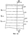
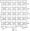
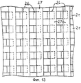
Ниже с помощью фиг.1-13 следует более подробное описание примеров запоминающих ячеек, согласно изобретению, и способа изготовления. Фиг.1 показывает устройство из запоминающих ячеек при виде сверху. Фиг.2 и 3 показывают отмеченное на фиг.1 сечение после различных этапов изготовления. Фиг.4 показывает альтернативное выполнение в сечении из фиг.3. Фиг.5 и 6 показывают формы выполнения из фиг.3 и 4 в отмеченных на фиг.1 и 4 сечениях. Фиг.7 показывает другой пример выполнения в сечении из фиг.3. Фиг.8 и 9 показывают сечения из фиг.5 и 3 для другой формы выполнения. Фиг.10, 12 и 13 показывают виды сверху, а фиг.11 показывает сечение для пояснения альтернативного способа изготовления.Below using FIGS. 1-13, a more detailed description of examples of storage cells according to the invention and a manufacturing method follows. Figure 1 shows a device from storage cells in a plan view. FIGS. 2 and 3 show the cross section indicated in FIG. 1 after various manufacturing steps. Figure 4 shows an alternative embodiment in cross section from figure 3. FIGS. 5 and 6 show the embodiment of FIGS. 3 and 4 in the sections indicated in FIGS. 1 and 4. Fig.7 shows another exemplary embodiment in cross section of Fig.3. Figs. 8 and 9 show sections from Figs. 5 and 3 for another embodiment. 10, 12 and 13 show top views, and FIG. 11 shows a cross section for explaining an alternative manufacturing method.
На фиг.1 изображена типичная топология предусмотренного в качестве памяти расположения запоминающих ячеек при cxeматичном виде сверху. В области, занимаемой утопленными разрядными шинами BL1, BL2,...,DLn и шинами WL1, WL2,...,WLn слов, расположенными над ними в большей близости к поверхности содержащего эту память чипа, находится предусмотренная в качестве памяти последовательность слоев, которая в описанных ниже примерах для упрощенного обозначения принимается как последовательность слоев оксид-нитрид-оксид или ОНО-структура. Эта ОНО-структура может быть прервана между разрядными шинами и шинами слов или иметь место на всей поверхности. На периферии памяти расположены управляющие элементы, которые включают в себя преимущественно выполненную по КМОП-технологии схемную логику для адресации памяти. Для выбора разрядных шин, которые ведут к областям истока и областям стока отдельных запоминающих ячеек, в этом примере имеются селективные транзисторы Т. Электроды затворов селективных транзисторов, например, для двоичной адресации поблочно соединены с шинами SG1, SG2,...,SGn селективных затворов. Такая архитектура памяти сама по себе известна.Figure 1 shows a typical topology of the location of the storage cells provided as a memory in a cchematic top view. In the region occupied by the recessed bit lines BL1, BL2, ..., DLn and word lines WL1, WL2, ..., WLn, located above them more closely to the surface of the chip containing this memory, there is a sequence of layers provided as a memory, which in the examples described below for simplified designation is taken as a sequence of oxide-nitride-oxide layers or an OHO structure. This IT structure may be interrupted between bit buses and word buses or occur on the entire surface. On the periphery of the memory are located control elements that include mainly logic circuitry designed for CMOS technology for addressing memory. To select the bit lines that lead to the source and drain areas of the individual memory cells, in this example there are selective transistors T. Gate electrodes of selective transistors, for example, for binary addressing, are block-wise connected to selective gate buses SG1, SG2, ..., SGn . Such a memory architecture is known per se.
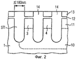
На фиг.2 в сечении изображен первый промежуточный продукт предпочтительного способа изготовления для примера фрагмента памяти. Изготовление осуществляется преимущественно в рамках КМОП-процесса, с помощью которого изготовляют и управляющую электронику. При этом принято верхнюю сторону полупроводникового тела или наращенного на подложку полупроводникового слоя покрывать сначала оксидом 12 и нитридом 13 контактных площадок. С применением подходящей техники масок вытравливают предусмотренные для памяти и STI-изоляции (shallow trench isolation) канавки преимущественно минимальной ширины (расстояние между областями истока и стока одной и той же запоминающей ячейки самое большее 180 нм) и заполняют диэлектрическим материалом, например оксидом.FIG. 2 is a sectional view showing a first intermediate product of a preferred manufacturing method for an example memory fragment. Manufacturing is carried out mainly in the framework of the CMOS process, with the help of which control electronics are also manufactured. In this case, the upper side of the semiconductor body or the semiconductor layer grown on the substrate is conventionally coated first with
Карманы р-тила и n-типа в соответствии с известным сам по себе КМОП-процессом выполняют за счет имплантации легирующей примеси в полупроводниковый материал. В зоне памяти изготовляют преимущественно карман р-типа 10. Тройной карман (triple well) с тремя расположенными друг в друге областями переменного знака электрической проводимости изготовляют для тех транзисторов, через которые шины слов памяти должны соединяться с отрицательным потенциалом с тем, чтобы методом горячих дырок (НH) с отрицательным потенциалом затвора можно было стирать содержимое запоминающих ячеек. Разрядные шины с содержащимися в них областями 3, 4 истока и стока отдельных запоминающих транзисторов изготовляют за счет дополнительной имплантации 11, в этом примере для проводимости n-типа. Область 4 стока действует каждый раз как область истока для последовательно граничащего транзистора. С помощью упомянутого выше способа программирования канальными горячими электронами (СНЕ) каждая запоминающая ячейка может хранить над областями истока и стока один бит информации, для чего при программировании исток и сток в принципиально симметричной структуре транзисторов меняются ролями.Pockets of r-tyl and n-type in accordance with the well-known CMOS process itself are performed by implanting a dopant in a semiconductor material. A p-
СНЕ-программирование и НН-стирание требуют жесткого перехода между проводимостями истока или стока и карманом. Поэтому преимущественно вместе с имплантацией легирующих примесей для истока и стока (в этом примере для проводимости n+-типа) легирующую примесь для электрической проводимости с противоположным знаком (в этом примере проводимость p+-типа за счет глубже проникающей имплантации вводят в граничащую с истоком или стоком долю слоя кармана (в этом примере легирование примесью р--типа) в большей концентрации.CHE programming and HH erasing require a hard transition between source or drain conductivity and pocket. Therefore, mainly along with the implantation of dopants for the source and drain (in this example for n + type conductivity), the dopant for electrical conductivity with the opposite sign (in this example, p + type conductivity is introduced into the adjacent to the source or the drain is the fraction of the pocket layer (in this example, doping with an admixture of p - type) in a higher concentration.
Канавки 14, предусмотренные для электродов затворов запоминающих транзисторов, вытравливают, нитрид и оксид контактных площадок удаляют и на всю поверхность наносят ОНО-структуру. ОНО-структура представляет собой преимущественно нижний ограничительный слой 5 из оксида толщиной 2,5-8 нм (bottom oxide, полученный преимущественно термически), запоминающий слой 6 из нитрида толщиной 1-5 нм (осажденный преимущественно посредством LPCVD [low-pressure chemical vapor deposition]) и верхний ограничительный слой 7 из оксида толщиной 3-12 нм (top oxide, осажденный). Канавки заполняют электропроводящим материалом, преимущественно нанесенным на всю поверхность проводящим легированным поликремнием, для изготовления электродов 2 затворов и слоя для образующих шины WL слов проводящих дорожек 8. Изготовляют еще уменьшающий сопротивление выводов слой 9, например, из силицида вольфрама или металлического слоя из вольфрама.The
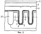
На фиг.3, изображающей в виде фрагмента отмеченное на фиг.1 сечение устройства из запоминающих ячеек, обозначен еще структурированный в виде полосы маскирующий слой 15, например износоустойчивая маска из нитрида, с помощью которого структурируют электроды затворов и шины слов за счет того, что не покрытый маской поликремний удаляют, например, посредством RIE (reactive ion etching).In Fig. 3, which depicts as a fragment the cross-section of the device from the storage cells marked in Fig. 1, a
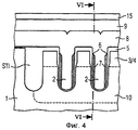
На фиг.4 изображено альтернативное выполнение, у которого перед нанесением слоя поликремния ОНО-структура анизотропно вытравлена до нижнего ограничительного слоя. Остатки ОНО-структуры имеются только на предусмотренных для хранения захваченных носителей заряда участках на стенках канавок. В остальном этот пример выполнения аналогичен примеру выполнения на фиг.3.Figure 4 shows an alternative embodiment, in which, before applying the polysilicon layer, the OHO structure is anisotropically etched to the lower bounding layer. The remains of the ONO structure are available only on the areas provided for storing the captured charge carriers on the walls of the grooves. Otherwise, this embodiment is similar to the example in FIG.
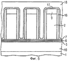
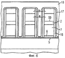
На фиг.5 в виде фрагмента изображено проходящее поперек шин слов сечение устройства из запоминающих ячеек. Форма выполнения соответствует фиг.3 с имеющейся на всей поверхности ОНО-структурой. После структурирования в виде полосы шин слов, причем ОНО-структура между шинами слов может быть удалена, по меньшей мере, частично, например, до нижнего ограничительного слоя 5, или также полностью до полупроводникового материала, изготовляют элементы-разделители 16 (spacer), являющиеся частью процесса изготовления управляющей КМОП-периферии. В случае удаления обозначенной на фиг.5 сплошной линией ОНО-структуры между шинами слов распорные элементы доходят соответственно до ограничительного слоя или полупроводникового материала. Нитридный слой 17 на всей поверхности покрывают планаризующим слоем 18, которым заполняют остаточные участки канавок между шинами слов. Перед нанесением планаризующего слоя 18 можно еще осуществить p+-имплантацию между шинами слов, с помощью которой можно улучшить изоляцию между отдельными запоминающими ячейками.Figure 5 in the form of a fragment shows the cross-section of the device from the storage cells passing across the word lines. The embodiment corresponds to FIG. 3 with an OHO structure present on the entire surface. After structuring in the form of a strip of word tires, moreover, the IT structure between the word buses can be removed at least partially, for example, to the
На фиг.6 изображен в соответствии с фиг.5 разрез формы выполнения на фиг.4. В указанном на фиг.4 направлении рассмотрения верхняя граница раздела нижнего ограничительного слоя 5 над областями 3, 4 истока и стока обозначена штриховой линией 50 в виде скрытого контура. Выше долей OHO-структуры, имеющихся в виде остатков наподобие распорок, имеется доля электрода 2 затвора. Нижний ограничительный слой 5 имеется на всей поверхности. Запоминающий слой 6 и верхний ограничительный слой 7 имеются только на боковых стенках канавок между электродом затвора и областями истока и стока. Граница между обозначенными поверхностями разреза этих слоев зависит от точного положения сечения, а также наклона стенок канавок и равномерности толщины слоев. Изображение на фиг.6 лишь поясняет принципиальную структуру, которая в остальном соответствует структуре на фиг.5.Figure 6 shows, in accordance with figure 5, a sectional view of the embodiment of figure 4. In the viewing direction indicated in FIG. 4, the upper interface of the
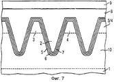
На фиг.7 изображен другой пример выполнения, у которого канавки выполнены V-образными. Соответствующие выполнению на фиг.3 подробности здесь обозначены теми же ссылочными позициями. Другое предпочтительное выполнение предусматривает выполнение V-образного наклона стенок канавок только в средней части канавок, тогда как стенки канавок сбоку от областей истока и стока проходят в основном круто вертикально. За счет этого посредством анизотропного вертикального травления ОНО-структуры можно удалить все, за исключением долей, оставшихся в верхней части стенок канавок, т.е. именно между изготовляемыми электродами затворов и областями истока и стока. Улучшенная изоляция электрода затвора от полупроводникового материала в нижней части канавок может быть достигнута тогда, когда после удаления запоминающего слоя нижний ограничительный слой (bottom oxide) оксидируют до большей толщины.Figure 7 shows another exemplary embodiment in which the grooves are made V-shaped. The details corresponding to the embodiment of FIG. 3 are denoted by the same reference numerals. Another preferred embodiment provides for the implementation of a V-shaped inclination of the walls of the grooves only in the middle part of the grooves, while the walls of the grooves on the side of the source and drain areas are generally steep vertically. Due to this, by means of anisotropic vertical etching of the OHO structure, everything can be removed, with the exception of the fractions remaining in the upper part of the walls of the grooves, i.e. It is between the manufactured gate electrodes and the source and drain areas. Improved isolation of the gate electrode from the semiconductor material in the lower part of the grooves can be achieved when, after removing the storage layer, the lower bound oxide layer is oxidized to a larger thickness.
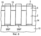
На фиг.8 и 9 другая форма выполнения изображена в сечениях, проходящих поперек шин слов и параллельно шинам слов. У этого выполнения диэлектрический материал предусмотренных для электродов затворов канавок 14 удаляют только на предусмотренных для шин слов участках. Предусмотренный для шин слов поликремний помещают только в освобожденные участки канавок. Поэтому можно отказаться от повторного заполнения открытых между шинами слов канавок. Для получения планарной поверхности перед открыванием заполненных диэлектрическим материалом (преимущественно оксидом) канавок 14 на всю поверхность наносят слой 19 из диэлектрического материала (преимущественно также оксида). Полосообразная маска, закрывающая поверхность слоя 19, имеющуюся между предусмотренными для шин слов участками, позволяет вытравить полосообразные отверстия для шин слов, а именно в канавках глубоко, а между канавками плоско в слое 19. В эти отверстия осаждают слои ОНО-структуры 5/6/7.In Figs. 8 and 9, another embodiment is shown in sections extending across the word lines and parallel to the word lines. In this embodiment, the dielectric material provided for the gate electrodes of the
Одно преимущество этого варианта состоит в том, что после осаждения поликремния для электродов 2 затворов и для предусмотренных для шин слов проводящих дорожек 8 канавки полностью заполнены. Поэтому уменьшающий сопротивление выводов слой 9 в рамках применяемого для компонентов управляющей схемы процесса силицирования (salicide) можно изготовить из силицида кобальта или силицида титана за счет того, что этот слой 9 сначала наносят из кобальта, который затем силицируют.One advantage of this embodiment is that after the deposition of polysilicon for the
На фиг.9, кроме того, видно, что нанесенный сначала нитрид 13 контактной площадки между предусмотренными для электродов затворов канавками был оставлен над разрядными шинами (в изображенном на фиг.9 разрезе из разрядных шин видно по одной области истока и области стока). Нитрид контактной площадки, если его не удаляют перед травлением канавок, может быть еще использован в качестве маски (травильный стоп-слой) для вытравливания канавок. При изготовлении изображенного на фиг.8 и 9 примера выполнения это имеет то особое преимущество, что при применении полосообразных масок для открывания участков, предусмотренных для шин слов и электродов затворов, имеющиеся еще между канавками доли нитрида 13 контактной площадки образуют целесообразный травильный стоп-слой, так что между разрядными шинами происходит травление в глубину, а области истока и стока остаются.In Fig. 9, in addition, it is seen that the first
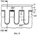
Альтернативный вариант описанного способа изготовления независимо от данного выполнения собственно запоминающей среды предусматривает нанесение и структурирование шин слов только после помещения электродов затворов в отверстия канавок. Это поясняется с помощью фиг.10-13. На фиг.10 изображена верхняя сторона подложки или полупроводникового тела, например кармана 10 р-типа, с предусмотренной ориентацией разрядных шин BLn-1, BLn, BLn+1. Преимущественно на эту сторону наносят оксид и нитрид контактных площадок. В полупроводниковом материале с применением полосообразной маски вытравливают канавки и заполняют их диэлектриком 21, что осуществляют преимущественно по типу STI с оксидом.An alternative to the described manufacturing method, irrespective of this embodiment of the storage medium itself, involves applying and structuring word lines only after placing the gate electrodes in the groove openings. This is explained using FIGS. 10-13. Figure 10 shows the upper side of the substrate or semiconductor body, for example p-
На фиг.11 изображено отмеченное на фиг.10 сечение, в котором видны оксид 22 и нитрид 23 контактных площадок в качестве слоев между заполненными канавками. Верхнюю сторону снабжают дополнительной полосообразной маской, которая ориентирована поперек, преимущественно перпендикулярно ориентации использованной до этого полосообразной маски. С применением этой дополнительной маски изготовляют отверстия в диэлектрике 21.In Fig.11 shows the cross section marked in Fig.10, in which
Фиг.12 показывает полученное на основе этого устройство. Полосообразные части 24 дополнительной маски, изображенные здесь кусками с штриховыми краями, проходят перпендикулярно вытравленным и заполненным канавкам. На участках верхней стороны, не закрытых дополнительной маской, диэлектрик 21 заполненных канавок удаляют, так что здесь образуются отверстия 25. Диэлектрик 21 в этих отверстиях удаляют до дна канавок.12 shows a device based on this. The strip-
Электроды затворов и расположенные с самосовмещением с ними шины слов могут быть выполнены на следующем этапе способа, как описано выше, с применением полосообразно структурированного слоя 19 из диэлектрического материала. Можно также снабдить сначала подзатворным диэлектриком отверстия 25 на соответствующих стенках и заполнить материалом электродов затворов и лишь после этого изготовить шины слов. У этого варианта изготовления слой предусмотренного для шин слов материала (например, W, WSi, поликремний) осаждают на всей поверхности, т.е. также на помещенные в отверстия электроды затворов. Если для электродов затворов и шин слов применяют один и тот же материал, то отверстия 25 могут быть заполнены также вместе с осаждением этого материала на всей поверхности верхней стороны. С применением третьей полосообразной маски шины слов структурируют из осажденного на всей поверхности слоя. С помощью третьей маски могут быть предпочтительно структурированы также электроды затворов транзисторов, расположенных на примыкающем к полю памяти участке управляющей схемы или в других логических областях интегрированной на том же чипе схемы. Так простым образом обеспечивается контактирование шин слов в шаге матрицы, т.е. на расстоянии соседних шин друг от друга, с компонентами управляющей схемы в целях управления запоминающими транзисторами с необходимыми напряжениями. Поскольку, однако, третью полосообразную маску не обязательно изготовлять точно в соответствии с предварительно использованной маской, при помощи которой были образованы отверстия 25, может произойти так, что шины слов будут немного смещены поперек своего продольного направления относительно электродов затворов, т.е. будут расположены не с полным совмещением с электродами затворов.The gate electrodes and word lines arranged with self-alignment with them can be performed in the next step of the method, as described above, using a strip-like
На фиг.13 также изображена верхняя сторона устройства в соответствии с фиг.12, после заполнения отверстий 25 электродами 26 затворов и структурирования шин 27 слов. Шины слов здесь обозначены преувеличенно четкими так, что они смещены вбок относительно электродов 26 затворов. Поэтому шины 27 слов перекрывают квадратные здесь при виде сверху электроды 26 затворов лишь частично, а именно на скрытом участке, обозначенном штриховыми линиями.On Fig also shows the upper side of the device in accordance with Fig, after filling the
В другом варианте способа изготовления сначала вытравливают и заполняют диэлектрическим материалом только те канавки, которые предусмотрены в качестве STI-канавок для окружающей устройство из запоминающих ячеек изоляции от управляющей периферии. Только с изготовлением легированных областей для разрядных шин, а также истока и стока в полупроводниковом материале вытравливают канавки для электродов затворов. Описанное выше выполнение обладает, однако, тем преимуществом, что канавки ориентируются с самосовмещением относительно внешней STI.In another embodiment of the manufacturing method, only those grooves that are provided as STI grooves for the surrounding device from the insulation memory cells from the control periphery are first etched and filled with dielectric material. Only with the manufacture of alloy areas for discharge tires, as well as the source and drain in the semiconductor material, grooves for the gate electrodes are etched. The implementation described above, however, has the advantage that the grooves are oriented with self-alignment relative to the external STI.
Вслед за структурированием шин слов осуществляют обычные и сами по себе известные этапы изготовления управляющих элементов. К ним относится, в частности, осуществляемая независимо от структуры запоминающих ячеек имплантация для областей истока и стока управляющих транзисторов, включая LDD- и Pocket-имплантаты. Разводка осуществляется посредством подходящего числа структурированных слоев металлизации, расположенных в промежуточных металлических диэлектриках. Из описания изготовления устройства из запоминающих ячеек, согласно изобретению, следует ее структура и, в частности, конструкция отдельной запоминающей ячейки, как она заявлена также отдельно.Following the structuring of word tires, the usual and in themselves known steps of manufacturing control elements are carried out. These include, in particular, implantation, independent of the structure of the storage cells, for the source and drain areas of control transistors, including LDD and Pocket implants. The wiring is carried out by means of a suitable number of structured metallization layers located in the intermediate metal dielectrics. From the description of the manufacture of the device from the storage cells, according to the invention, it follows its structure and, in particular, the design of a separate storage cell, as it is also stated separately.
Claims (11)
Applications Claiming Priority (4)
| Application Number | Priority Date | Filing Date | Title |
|---|---|---|---|
| DE10039441A DE10039441A1 (en) | 2000-08-11 | 2000-08-11 | Memory cell, memory cell arrangement and manufacturing method |
| DE10039441.8 | 2000-08-11 | ||
| US09/900,654 US20020024092A1 (en) | 2000-08-11 | 2001-07-06 | Memory cell, memory cell arrangement and fabrication method |
| US09/900,654 | 2001-07-06 |
Publications (2)
| Publication Number | Publication Date |
|---|---|
| RU2003106401A RU2003106401A (en) | 2004-07-20 |
| RU2247441C2 true RU2247441C2 (en) | 2005-02-27 |
Family
ID=26006676
Family Applications (1)
| Application Number | Title | Priority Date | Filing Date |
|---|---|---|---|
| RU2003106401/28A RU2247441C2 (en) | 2000-08-11 | 2001-08-06 | Memory device and its manufacturing process |
Country Status (9)
| Country | Link |
|---|---|
| US (1) | US6844584B2 (en) |
| EP (1) | EP1307920A2 (en) |
| JP (1) | JP2004517464A (en) |
| CN (1) | CN100446258C (en) |
| BR (1) | BR0113164A (en) |
| MX (1) | MXPA03001223A (en) |
| RU (1) | RU2247441C2 (en) |
| TW (1) | TWI244199B (en) |
| WO (1) | WO2002015276A2 (en) |
Cited By (2)
| Publication number | Priority date | Publication date | Assignee | Title |
|---|---|---|---|---|
| RU2543668C2 (en) * | 2012-08-27 | 2015-03-10 | Федеральное государственное бюджетное учреждение науки Физико-технический институт им. Ф.Ф. Иоффе Российской академии наук | Field transistor with memory cell |
| RU2817107C1 (en) * | 2021-07-01 | 2024-04-10 | Чансинь Мемори Текнолоджис, Инк. | Semiconductor structure and method of its manufacturing |
Families Citing this family (30)
| Publication number | Priority date | Publication date | Assignee | Title |
|---|---|---|---|---|
| DE10204868B4 (en) * | 2002-02-06 | 2007-08-23 | Infineon Technologies Ag | Memory cell with trench storage transistor and oxide-nitride-oxide dielectric |
| DE10219917A1 (en) * | 2002-05-03 | 2003-11-13 | Infineon Technologies Ag | Trench transistor for a storage cell comprises a trench with vertical side walls, a thin dielectric layer, and oxide layers on semiconductor material arranged on base of the trench and/or on part of the upper side of semiconductor body |
| DE10225410A1 (en) | 2002-06-07 | 2004-01-08 | Infineon Technologies Ag | Process for the production of NROM memory cells with trench transistors |
| DE10226964A1 (en) | 2002-06-17 | 2004-01-08 | Infineon Technologies Ag | Method for manufacturing an NROM memory cell arrangement |
| DE10229065A1 (en) * | 2002-06-28 | 2004-01-29 | Infineon Technologies Ag | Method for producing an NROM memory cell array |
| KR100885910B1 (en) * | 2003-04-30 | 2009-02-26 | 삼성전자주식회사 | Nonvolatile semiconductor memory device having gate stack comprising OHAOxide-Hafnium oxide-Aluminium oxide film and method for manufacturing the same |
| US6979857B2 (en) * | 2003-07-01 | 2005-12-27 | Micron Technology, Inc. | Apparatus and method for split gate NROM memory |
| DE10333549B3 (en) * | 2003-07-23 | 2005-01-13 | Infineon Technologies Ag | Charge trapping memory cell used as transistor comprises semiconductor body or substrate having upper side with curve in channel region |
| US6987689B2 (en) * | 2003-08-20 | 2006-01-17 | International Business Machines Corporation | Non-volatile multi-stable memory device and methods of making and using the same |
| US6977412B2 (en) * | 2003-09-05 | 2005-12-20 | Micron Technology, Inc. | Trench corner effect bidirectional flash memory cell |
| US6965143B2 (en) * | 2003-10-10 | 2005-11-15 | Advanced Micro Devices, Inc. | Recess channel flash architecture for reduced short channel effect |
| US7041545B2 (en) * | 2004-03-08 | 2006-05-09 | Infineon Technologies Ag | Method for producing semiconductor memory devices and integrated memory device |
| KR100594266B1 (en) * | 2004-03-17 | 2006-06-30 | 삼성전자주식회사 | SONOS type memory device |
| US20060043463A1 (en) * | 2004-09-01 | 2006-03-02 | Taiwan Semiconductor Manufacturing Company, Ltd. | Floating gate having enhanced charge retention |
| TWI270199B (en) * | 2005-01-31 | 2007-01-01 | Powerchip Semiconductor Corp | Non-volatile memory and manufacturing method and operating method thereof |
| US7186607B2 (en) * | 2005-02-18 | 2007-03-06 | Infineon Technologies Ag | Charge-trapping memory device and method for production |
| US7196008B1 (en) * | 2005-03-23 | 2007-03-27 | Spansion Llc | Aluminum oxide as liner or cover layer to spacers in memory device |
| DE102005024951A1 (en) * | 2005-05-31 | 2006-12-14 | Infineon Technologies Ag | Semiconductor memory device |
| US7468299B2 (en) * | 2005-08-04 | 2008-12-23 | Macronix International Co., Ltd. | Non-volatile memory cells and methods of manufacturing the same |
| US7292478B2 (en) * | 2005-09-08 | 2007-11-06 | Macronix International Co., Ltd. | Non-volatile memory including charge-trapping layer, and operation and fabrication of the same |
| US20070221979A1 (en) * | 2006-03-22 | 2007-09-27 | Dirk Caspary | Method for production of memory devices and semiconductor memory device |
| US20070257293A1 (en) * | 2006-05-08 | 2007-11-08 | Josef Willer | Semiconductor memory device and method for production of the semiconductor memory device |
| JP2008166528A (en) * | 2006-12-28 | 2008-07-17 | Spansion Llc | Semiconductor device and its manufacturing method |
| US7778073B2 (en) | 2007-10-15 | 2010-08-17 | Qimonda Ag | Integrated circuit having NAND memory cell strings |
| JP5405737B2 (en) * | 2007-12-20 | 2014-02-05 | スパンション エルエルシー | Semiconductor device and manufacturing method thereof |
| JP2009277782A (en) * | 2008-05-13 | 2009-11-26 | Oki Semiconductor Co Ltd | Semiconductor memory and its production process |
| US8304840B2 (en) | 2010-07-29 | 2012-11-06 | Taiwan Semiconductor Manufacturing Company, Ltd. | Spacer structures of a semiconductor device |
| US9412790B1 (en) * | 2012-12-04 | 2016-08-09 | Crossbar, Inc. | Scalable RRAM device architecture for a non-volatile memory device and method |
| CN108735772B (en) * | 2017-04-14 | 2020-08-21 | 上海磁宇信息科技有限公司 | Shared high-density random access memory architecture |
| CN108735773A (en) * | 2017-04-14 | 2018-11-02 | 上海磁宇信息科技有限公司 | A kind of ultra high density random access memory framework |
Family Cites Families (18)
| Publication number | Priority date | Publication date | Assignee | Title |
|---|---|---|---|---|
| US3731163A (en) * | 1972-03-22 | 1973-05-01 | United Aircraft Corp | Low voltage charge storage memory element |
| SU752476A1 (en) | 1978-07-24 | 1980-07-30 | Предприятие П/Я А-1889 | Storage cell |
| DE2946864A1 (en) * | 1978-11-27 | 1980-06-04 | Texas Instruments Inc | Permanent metal insulator semiconductor memory cell - has silica, silicon nitride, silica and silicon nitride or rutile films to increase efficiency and speed |
| US4360900A (en) * | 1978-11-27 | 1982-11-23 | Texas Instruments Incorporated | Non-volatile semiconductor memory elements |
| US4242737A (en) * | 1978-11-27 | 1980-12-30 | Texas Instruments Incorporated | Non-volatile semiconductor memory elements |
| JP2662076B2 (en) * | 1990-05-02 | 1997-10-08 | 松下電子工業株式会社 | Nonvolatile semiconductor memory device and method of manufacturing the same |
| DE19545903C2 (en) | 1995-12-08 | 1997-09-18 | Siemens Ag | Read-only memory cell arrangement and method for its production |
| DE19600423C2 (en) | 1996-01-08 | 2001-07-05 | Siemens Ag | Electrically programmable memory cell arrangement and method for its production |
| DE19600422C1 (en) | 1996-01-08 | 1997-08-21 | Siemens Ag | Electrically programmable memory cell arrangement and method for its production |
| US5768192A (en) | 1996-07-23 | 1998-06-16 | Saifun Semiconductors, Ltd. | Non-volatile semiconductor memory cell utilizing asymmetrical charge trapping |
| US5817560A (en) | 1996-09-12 | 1998-10-06 | Advanced Micro Devices, Inc. | Ultra short trench transistors and process for making same |
| US5808340A (en) * | 1996-09-18 | 1998-09-15 | Advanced Micro Devices, Inc. | Short channel self aligned VMOS field effect transistor |
| US5966603A (en) * | 1997-06-11 | 1999-10-12 | Saifun Semiconductors Ltd. | NROM fabrication method with a periphery portion |
| US5973358A (en) * | 1997-07-01 | 1999-10-26 | Citizen Watch Co., Ltd. | SOI device having a channel with variable thickness |
| US6768165B1 (en) | 1997-08-01 | 2004-07-27 | Saifun Semiconductors Ltd. | Two bit non-volatile electrically erasable and programmable semiconductor memory cell utilizing asymmetrical charge trapping |
| JP3544833B2 (en) * | 1997-09-18 | 2004-07-21 | 株式会社東芝 | Semiconductor device and manufacturing method thereof |
| TW383427B (en) * | 1998-04-03 | 2000-03-01 | United Microelectronics Corp | Method for etching tantalum oxide |
| EP0967654A1 (en) * | 1998-06-26 | 1999-12-29 | EM Microelectronic-Marin SA | Non-volatile semiconductor memory device |
-
2001
- 2001-08-06 EP EP01962611A patent/EP1307920A2/en not_active Withdrawn
- 2001-08-06 CN CNB018139574A patent/CN100446258C/en not_active Expired - Fee Related
- 2001-08-06 BR BR0113164-8A patent/BR0113164A/en not_active IP Right Cessation
- 2001-08-06 RU RU2003106401/28A patent/RU2247441C2/en not_active IP Right Cessation
- 2001-08-06 MX MXPA03001223A patent/MXPA03001223A/en unknown
- 2001-08-06 WO PCT/DE2001/002997 patent/WO2002015276A2/en not_active Application Discontinuation
- 2001-08-06 JP JP2002520306A patent/JP2004517464A/en active Pending
- 2001-08-08 TW TW090119349A patent/TWI244199B/en not_active IP Right Cessation
- 2001-08-09 US US09/927,573 patent/US6844584B2/en not_active Expired - Lifetime
Cited By (2)
| Publication number | Priority date | Publication date | Assignee | Title |
|---|---|---|---|---|
| RU2543668C2 (en) * | 2012-08-27 | 2015-03-10 | Федеральное государственное бюджетное учреждение науки Физико-технический институт им. Ф.Ф. Иоффе Российской академии наук | Field transistor with memory cell |
| RU2817107C1 (en) * | 2021-07-01 | 2024-04-10 | Чансинь Мемори Текнолоджис, Инк. | Semiconductor structure and method of its manufacturing |
Also Published As
| Publication number | Publication date |
|---|---|
| TWI244199B (en) | 2005-11-21 |
| US6844584B2 (en) | 2005-01-18 |
| WO2002015276A3 (en) | 2002-06-06 |
| MXPA03001223A (en) | 2003-09-22 |
| JP2004517464A (en) | 2004-06-10 |
| US20030015752A1 (en) | 2003-01-23 |
| CN1446378A (en) | 2003-10-01 |
| CN100446258C (en) | 2008-12-24 |
| WO2002015276A2 (en) | 2002-02-21 |
| EP1307920A2 (en) | 2003-05-07 |
| BR0113164A (en) | 2003-06-24 |
Similar Documents
| Publication | Publication Date | Title |
|---|---|---|
| RU2247441C2 (en) | Memory device and its manufacturing process | |
| US20020024092A1 (en) | Memory cell, memory cell arrangement and fabrication method | |
| US6548861B2 (en) | Memory cell, memory cell arrangement and fabrication method | |
| US7420256B2 (en) | Nonvolatile semiconductor memory device having a gate stack and method of manufacturing the same | |
| US6888194B2 (en) | Nonvolatile semiconductor memory device, manufacturing method thereof, and operating method thereof | |
| EP1399965B1 (en) | Isolation of sonos devices | |
| US7626226B2 (en) | Method for improving erase saturation in non-volatile memory devices and devices obtained thereof | |
| KR100474176B1 (en) | Method for producing a multi-bit memory cell | |
| KR100967255B1 (en) | A semiconductor integrated circuit device and a method of manufacturing the same | |
| US7517757B2 (en) | Non-volatile memory device having dual gate and method of forming the same | |
| US9231115B2 (en) | Semiconductor device and manufacturing method thereof | |
| US20060043457A1 (en) | Nonvolatile semiconductor memory device having a recessed gate and a charge trapping layer and methods of forming the same, and methods of operating the same | |
| EP1918984A2 (en) | Charge-trapping device with cylindrical channel and method of manufacturing thereof | |
| JP2002313967A (en) | Semiconductor device and its manufacturing method | |
| US20190198681A1 (en) | Semiconductor device and method of manufacturing the same | |
| WO2003001601A2 (en) | Spacer etch mask for sonos memory | |
| US20080080249A1 (en) | Non-volatile memory, fabricating method and operating method thereof | |
| EP4222744A1 (en) | Split-gate non-volatile memory cells with erase gates disposed over word line gates, and method of making same | |
| EP1748473A2 (en) | Non-volatile memory transistor with distributed charge storage sites | |
| EP1903602A2 (en) | Non-volatile memory transistor | |
| US20220157964A1 (en) | Semiconductor device | |
| EP1748472A1 (en) | Non-volatile memory transistor | |
| US20080025084A1 (en) | High aspect ration bitline oxides | |
| CN112736085A (en) | Method for manufacturing semiconductor device |
Legal Events
| Date | Code | Title | Description |
|---|---|---|---|
| MM4A | The patent is invalid due to non-payment of fees |
Effective date: 20170807 |