RU2114503C1 - Structure-borne noise rejection device - Google Patents
Structure-borne noise rejection device Download PDFInfo
- Publication number
- RU2114503C1 RU2114503C1 RU94026053A RU94026053A RU2114503C1 RU 2114503 C1 RU2114503 C1 RU 2114503C1 RU 94026053 A RU94026053 A RU 94026053A RU 94026053 A RU94026053 A RU 94026053A RU 2114503 C1 RU2114503 C1 RU 2114503C1
- Authority
- RU
- Russia
- Prior art keywords
- input
- multipliers
- output
- inputs
- adder
- Prior art date
Links
- 238000002955 isolation Methods 0.000 claims 1
- 230000001629 suppression Effects 0.000 abstract description 4
- 239000000126 substance Substances 0.000 abstract 1
- 239000000203 mixture Substances 0.000 description 6
- 238000010586 diagram Methods 0.000 description 2
- 230000036039 immunity Effects 0.000 description 2
- 238000001228 spectrum Methods 0.000 description 2
- 101001086861 Hydrogenobacter thermophilus (strain DSM 6534 / IAM 12695 / TK-6) Putative phosphoserine phosphatase 2 Proteins 0.000 description 1
- 239000008186 active pharmaceutical agent Substances 0.000 description 1
- 230000015572 biosynthetic process Effects 0.000 description 1
- 230000003111 delayed effect Effects 0.000 description 1
- 238000000605 extraction Methods 0.000 description 1
- 230000007274 generation of a signal involved in cell-cell signaling Effects 0.000 description 1
- 238000000034 method Methods 0.000 description 1
Images
Landscapes
- Noise Elimination (AREA)
Abstract
Description
Изобретение относится к радиосвязи и может найти применение в асинхронно-адресных системах связи с широкополосными сигналами. The invention relates to radio communications and may find application in asynchronous-address communication systems with broadband signals.
Известно устройство подавления структурных помех по а.с. N 930719, содержащее первый и второй перемножители, подключенные ко входам сумматора и блока выделения информации, третий перемножитель, соединенный с блоком ФАПЧ и блоком формирования опорных сигналов, первый и второй полосовые фильтры и дешифратор. Работа устройства основана на формировании оценки помехи за счет подавления во входной смеси полезного сигнала с последующей компенсацией помехи с использованием полученной помехи. A device for suppressing structural interference in AS N 930719, containing the first and second multipliers connected to the inputs of the adder and the information extraction unit, the third multiplier connected to the PLL and the reference signal generation unit, the first and second bandpass filters and a decoder. The operation of the device is based on the formation of an interference estimate by suppressing a useful signal in the input mixture, followed by compensation for the interference using the resulting interference.
Известно устройство по а.с. N 1107327, содержащее первый и второй перемножители, первый и второй полосовые фильтры, ГПСП, блок ФАПЧ, коммутатор, блок выделения информации. В этом устройстве также формируется оценка помехи, которая используется для последующей компенсации помех. A device is known by A.S. N 1107327, containing the first and second multipliers, the first and second band-pass filters, GPS, PLL, switch, information allocation unit. This device also generates an interference estimate, which is used for subsequent interference compensation.
Недостатком этих известных устройств является малая степень подавления помех. A disadvantage of these known devices is the low degree of interference suppression.
Наиболее близким по технической сущности к предлагаемому является устройство по а.с. N 1338078, структурная схема которого приведена на фиг. 1, где обозначено: 1 - перемножитель, 2 - генератор копии сигнала, 3 - интегратор, 4 - ключ, 5 - блок сравнения, 6 - формирователь порога, 7 - режекторный фильтр, 8 - перемножитель, 9 - вычитатель, 10 - элемент задержки, 11 - усилитель. The closest in technical essence to the proposed one is a device for AS N 1338078, the structural diagram of which is shown in FIG. 1, where it is indicated: 1 - multiplier, 2 - signal copy generator, 3 - integrator, 4 - key, 5 - comparison unit, 6 - threshold shaper, 7 - notch filter, 8 - multiplier, 9 - subtractor, 10 - delay element , 11 - amplifier.
Устройство содержит последовательно соединенные вычитатель 9, первый вход которого является входом устройства, перемножитель 1, режекторный фильтр 7, перемножитель 8, усилитель 11, выход которого соединен со вторым входом вычитателя 9. Выход перемножителя 1 соединен также через интегратор 3, ключ 4 с блоком сравнения 5, второй вход которого соединен с выходом формирователя порога 6. Выход генератора ПСП 2 соединен со входом перемножителя 1 и через элемент задержки 10 со входом перемножителя 8. Второй выход генератора 2 соединен со вторым входом ключа 4. The device contains a series-connected subtractor 9, the first input of which is the input of the device, multiplier 1, notch filter 7,
Работает устройство следующим образом. The device operates as follows.
Входной сигнал, представляющий собой смесь полезного широкополосного сигнала и помех, поступает на вход вычитателя 9, где из него вычитается сигнал, сформированный в кольце обратной связи и поступающий с выхода усилителя 11. С выхода вычитателя 9 сигнал поступает на перемножитель 1, где перемножается с опорным сигналом, формируемым генератором 2. Результат перемножения накапливается в интеграторе 3 и через ключ 4, управляемый генератором 2, подается на блок сравнения 5, где сравнивается с пороговым сигналом, сформированным в формирователе 6. The input signal, which is a mixture of useful broadband signal and noise, is fed to the input of the subtractor 9, where the signal generated in the feedback ring and supplied from the output of the
Одновременно сигнал с выхода перемножителя 1 поступает в кольцо обратной связи, содержащее режекторный фильтр 7, перемножитель 8 и усилитель с регулируемым коэффициентом усиления. В результате перемножения с копией сигнала полезный сигнал ШПС на выходе перемножителя сворачивается в узкополосный сигнал, а узкополосные помехи превращаются в широкополосные помехи с базой Б, равной базе полезного ШПС. В режекторном фильтре 7 режектируется свернутый полезный сигнал и части спектра помех, попадающих в его полосу. Таким образом, на выход режекторного фильтра 7 полезный сигнал не проходит. С выхода режекторного фильтра 7 помехи поступают на перемножитель 8, где путем перемножения с той же копией полезного сигнала, задержанной в элементе задержки 10 на величину задержки τ , равную задержке помех в режекторном фильтре 7, сворачиваются в узкополосные сигналы, т.е. приводятся к своему первоначальному виду. С выхода перемножителя 8 помехи через усилитель 11 подаются на вход вычитателя 9. Таким образом, на первом входе вычитателя 9 присутствует полезный сигнал и помехи, а на втором его входе только помехи. В вычитателе 9 обеспечивается противофазность сигналов, поступающих по его входам. В процессе настройки коэффициент усиления усилителя с регулируемым коэффициентом усиления выбирается таким, чтобы обеспечивалось равенство амплитуд сигналов на его выходе. Поскольку полезный сигнал поступает только по первому выходу вычитателя 9, а помехи - как по первому, так и по второму его входам, то сигнал на его выход проходит без искажений, а помехи в нем компенсируются. At the same time, the signal from the output of the multiplier 1 enters a feedback ring containing a notch filter 7, a
Недостатком устройства-прототипа является низкая помехоустойчивость к структурным помехам. The disadvantage of the prototype device is the low noise immunity to structural interference.
Для повышения помехоустойчивости в устройство, содержащее первый и второй перемножители, режекторный фильтр, элемент задержки, введены (n - 1) первых перемножителей, первый сумматор, входы которого соединены с выходами n первых перемножителей, а выход со входом режекторного фильтра, последовательно соединенные развязывающее устройство, вход которого соединен с выходом режекторного фильтра, (n - 1) вторых перемножителей, второй сумматор, аттенюатор, коммутатор, первый вход которого соединен через элемент задержки со входом устройства, а управляющий вход - с выходом схемы "ИЛИ", а также n ключей, управляющие входы которых объединены со входами схемы "ИЛИ" и соединены с источником команды о наличии (или отсутствии) синхронизации приемника ЦС, вторые входы ключей соединены с источниками ПСП соответствующего приемника ЦС, а выходы ключей соединены со вторыми входами n первых перемножителей, а через n элементов задержки со вторыми входами n вторых перемножителей. To increase the noise immunity, a device containing the first and second multipliers, a notch filter, a delay element, introduces (n - 1) first multipliers, a first adder, the inputs of which are connected to the outputs of the n first multipliers, and the output to the input of the notch filter, decoupling device connected in series the input of which is connected to the output of the notch filter, (n - 1) second multipliers, the second adder, attenuator, switch, the first input of which is connected through the delay element to the input of the device, and the control the input input - with the output of the OR circuit, as well as n keys whose control inputs are combined with the inputs of the OR circuit and connected to the command source about the presence (or absence) of synchronization of the CA receiver, the second key inputs are connected to the SRP sources of the corresponding CA receiver , and the key outputs are connected to the second inputs of the n first multipliers, and through n delay elements with the second inputs of the n second multipliers.
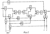
Структурная схема заявляемого устройства представлена на фиг. 2, где обозначено: 11...1n - перемножители, 2 - сумматор, 3 - режекторный фильтр, 4 - развязывающее устройство, 51...5n - перемножитель, 6 - сумматор, 7 - аттенюатор, 8 - коммутатор, 91...9n - ключ, 10 - схема "ИЛИ", 11, 12 - элементы задержки.The structural diagram of the inventive device is shown in FIG. 2, where it is indicated: 1 1 ... 1 n - multipliers, 2 - adder, 3 - notch filter, 4 - decoupling device, 5 1 ... 5 n - multiplier, 6 - adder, 7 - attenuator, 8 - switch , 9 1 ... 9 n is the key, 10 is the OR circuit, 11, 12 are delay elements.
Устройство содержит n перемножителей 1, объединенные входы которых являются входами устройства. Выходы перемножителей 1 соединены со входами сумматора 2, выход которого через режекторный фильтр 3 соединен со входом развязывающего устройства 4. Выходы развязывающего устройства 4 соединены со входами второй группы из n перемножителей 5, выходы которых соединены со входами сумматора 6. Выход сумматора 6 через аттенюатор 7 соединен со вторым входом коммутатора 8, первый вход которого соединен со входом устройства через элемент задержки 11. Вторые входы перемножителей 1 соединены с выходами ключей 9. С этими же выходами ключей 9 через элементы задержки 12 соединены вторые входы перемножителей 5. Входы ключей 9 соединены с источниками ПСП соответствующих приемников. Вторые входы ключей 9 и входы схемы "ИЛИ" 10 объединены и соединены с источниками команды о наличии (или отсутствии) синхронизации каждого приемника со своим сигналом. Выход схемы "ИЛИ" 10 соединен с третьим входом коммутатора 8. The device contains n multipliers 1, the combined inputs of which are the inputs of the device. The outputs of the multipliers 1 are connected to the inputs of the adder 2, the output of which through a notch filter 3 is connected to the input of the decoupling device 4. The outputs of the decoupling device 4 are connected to the inputs of the second group of
Работает устройство следующим образом. The device operates as follows.
Входная смесь, содержащая полезный ШПС и структурные помехи, поступает на первый вход коммутатора 8 через элемент задержки 11, а на второй его вход через цепочку элементов 1 - 7. На вторые входы перемножителей 1 и 5 через ключи 9 (91...9n) подаются ПСП. При этом на каждый i-тый перемножитель через ключ 9i (i = 1,...n) подается ПСП i от соответствующего этому перемножителю приемника, расположенного на ЦС асинхронно-адресной системы связи. Управление ключом 9i осуществляется командой CCi от i-го приемника. В том случае, когда i-тый приемник вошел в синхронизм с сигналом своего абонента, на его выходе формируется команда "1". При отсутствии синхронизации "0".The input mixture containing useful SHPS and structural noise is fed to the first input of
Сигналы с выходов перемножителей суммируются в сумматоре 2, режектируются режекторным фильтром 3 и через развязывающее устройство 4 результат режекции подается на перемножители 5. Структурная помеха от i-той АС асинхронно-адресной системы связи за счет перемножения с синхронной с ней опорной ПСПi сворачивается в узкополосную помеху, которая режектируется режекторным фильтром 3 и поэтому не поступает на вход коммутатора 8. В то же время полезный ШПС не сворачивается в перемножителях 1, а получает в них дополнительную манипуляцию, которая снижается в перемножителях 5 за счет перемножения с теми же опорными ПСП.The signals from the outputs of the multipliers are summed in the adder 2, rejected by a notch filter 3, and through the decoupling device 4, the result of the rejection is fed to the
Таким образом на вход коммутатора 8 поступает полезный ШПС, а помехи не проходят. Управление коммутатором 8 осуществляется командами CC1...CCn, которые поступают от приемников ЦС (n = 1, N - 1) на управляющий вход через схему "ИЛИ". То есть если хотя бы один из n приемников ЦС вошел в синхронизм со своим абонентом, то на выходе схемы "ИЛИ" 10 сформируется "1", которая подключит к выходу устройства аттенюатор 7, а выход элемента задержки 11 отключит. В данном случае входная смесь пройдет через блоки 1 - 8, при этом от нее отрежектируются структурные помехи от соответствующих абонентов. В том случае, когда ни один из приемников ЦС не вошел в синхронизм, на выходе схемы "ИЛИ" формируется "0", коммутатор 8 подключает к выходу устройства выход блока 11 и входная смесь проходит на выход устройства.Thus, the useful ShPS is supplied to the input of the
Элемент задержки 11 вводится при необходимости для выравнивания по задержке ШПС, проходящего по верхней и нижней ветвям. Элементы задержки 12 вводятся также при необходимости для выравнивания по времени ШПС и опорных ПСП на входах перемножителей 5. Такая необходимость возникает при высоких тактовых частотах ПСП. The
Пусть в асинхронной системе связи имеется ЦС, на которой установлен передатчик и n приемников, каждый из которых принимает сигнал от своей АС, содержащей передатчик и приемник. В каждый из приемников ЦС устанавливается устройство-прототип или заявляемое устройство. При этом на входы заявляемого устройства, устанавливаемого в i-тый приемник, подаются n - 1 ПСП других приемников и их n - 1 сигналы синхронизации. В устройстве-прототипе в первом перемножителе осуществляется свертка полезного сигнала, который режектируется в режекторном фильтре, и дополнительная манипуляция помех, которая снимается во втором перемножителе. Таким образом на первый вход вычитателя подается смесь сигнала и помех, и на второй - только помехи, за счет чего обеспечивается их компенсация. Однако степень компенсации ограничивается величиной 20 - 40 дБ, что определяется возможностями схем компенсации в условиях разброса параметров элементов схемы. Кроме того, за счет вырезания части спектра помехи режекторным фильтром в принципе невозможна полная ее компенсация. При этом нескомпенсированная часть помехи попадает в такт сигнала и не может быть от него отделена при дальнейшей обработке. Suppose that in an asynchronous communication system there is a DS on which a transmitter and n receivers are installed, each of which receives a signal from its AS containing the transmitter and receiver. A prototype device or the inventive device is installed in each of the CA receivers. At the same time, n - 1 SRP of other receivers and their n - 1 synchronization signals are fed to the inputs of the inventive device installed in the i-th receiver. In the prototype device in the first multiplier, the useful signal is convolved, which is rejected in the notch filter, and additional interference manipulation is removed in the second multiplier. Thus, a mixture of signal and interference is fed to the first input of the subtractor, and only interference is supplied to the second input, due to which their compensation is ensured. However, the degree of compensation is limited to 20–40 dB, which is determined by the capabilities of the compensation schemes in the conditions of a variation in the parameters of the circuit elements. In addition, due to cutting out part of the interference spectrum by a notch filter, in principle, its full compensation is impossible. In this case, the uncompensated part of the interference falls into the clock cycle of the signal and cannot be separated from it during further processing.
В заявляемом устройстве степень ослабления структурных помех определяется затуханием в полосе режекторного фильтра, которая может составлять 60 - 80 дБ. Степень подавления помех в схемах режекции значительно выше, чем в схемах компенсации. При этом выигрыш в степени подавления помех составляет 20 - 60 дБ, что и доказывает достижение поставленной цели. In the inventive device, the degree of attenuation of structural interference is determined by the attenuation in the band of the notch filter, which can be 60 - 80 dB. The degree of interference suppression in rejection schemes is much higher than in compensation schemes. In this case, the gain in the degree of suppression of interference is 20 - 60 dB, which proves the achievement of the goal.
Claims (1)
Priority Applications (1)
| Application Number | Priority Date | Filing Date | Title |
|---|---|---|---|
| RU94026053A RU2114503C1 (en) | 1994-07-15 | 1994-07-15 | Structure-borne noise rejection device |
Applications Claiming Priority (1)
| Application Number | Priority Date | Filing Date | Title |
|---|---|---|---|
| RU94026053A RU2114503C1 (en) | 1994-07-15 | 1994-07-15 | Structure-borne noise rejection device |
Publications (2)
| Publication Number | Publication Date |
|---|---|
| RU94026053A RU94026053A (en) | 1996-05-20 |
| RU2114503C1 true RU2114503C1 (en) | 1998-06-27 |
Family
ID=20158443
Family Applications (1)
| Application Number | Title | Priority Date | Filing Date |
|---|---|---|---|
| RU94026053A RU2114503C1 (en) | 1994-07-15 | 1994-07-15 | Structure-borne noise rejection device |
Country Status (1)
| Country | Link |
|---|---|
| RU (1) | RU2114503C1 (en) |
Cited By (1)
| Publication number | Priority date | Publication date | Assignee | Title |
|---|---|---|---|---|
| RU2574860C1 (en) * | 2014-12-24 | 2016-02-10 | Открытое акционерное общество научно-внедренческое предприятие "ПРОТЕК" | Detector with interference canceller |
Citations (1)
| Publication number | Priority date | Publication date | Assignee | Title |
|---|---|---|---|---|
| SU1107327A1 (en) * | 1983-02-08 | 1984-08-07 | Московский Ордена Трудового Красного Знамени Электротехнический Институт Связи | Device for correlation receiving of pseudorandom phase-shift keyed signals |
-
1994
- 1994-07-15 RU RU94026053A patent/RU2114503C1/en not_active IP Right Cessation
Patent Citations (1)
| Publication number | Priority date | Publication date | Assignee | Title |
|---|---|---|---|---|
| SU1107327A1 (en) * | 1983-02-08 | 1984-08-07 | Московский Ордена Трудового Красного Знамени Электротехнический Институт Связи | Device for correlation receiving of pseudorandom phase-shift keyed signals |
Non-Patent Citations (1)
| Title |
|---|
| SU, авторско е свидетельство, 1338078, кл. H 04 B 1/10, 1987. * |
Cited By (1)
| Publication number | Priority date | Publication date | Assignee | Title |
|---|---|---|---|---|
| RU2574860C1 (en) * | 2014-12-24 | 2016-02-10 | Открытое акционерное общество научно-внедренческое предприятие "ПРОТЕК" | Detector with interference canceller |
Also Published As
| Publication number | Publication date |
|---|---|
| RU94026053A (en) | 1996-05-20 |
Similar Documents
| Publication | Publication Date | Title |
|---|---|---|
| US4470138A (en) | Non-orthogonal mobile subscriber multiple access system | |
| US4475214A (en) | CW Interference cancelling sytem for spread spectrum signals utilizing active coherent detection | |
| RU2034403C1 (en) | Noise suppressor for broadband signal receivers | |
| RU2114503C1 (en) | Structure-borne noise rejection device | |
| RU2166232C2 (en) | Structural noise suppressing device for broadband signal receivers | |
| RU2001525C1 (en) | Device for reception of broadband signals | |
| SU1688416A1 (en) | Correlation processing unit for broadband signals affected by narrow- band interference | |
| RU2157049C1 (en) | Device for compensating noise in broad band receivers | |
| RU2020762C1 (en) | Device for detection of wide-band signals | |
| SU1338078A1 (en) | Wide-band signal correlation processing device | |
| RU2114502C1 (en) | Spur-interference rejection device | |
| RU2143175C1 (en) | Structure noise compensation device for wide- band signal receivers | |
| RU2143783C1 (en) | Noise suppression device for code-division satellite communication systems | |
| RU2143174C1 (en) | Structure noise suppression device for wide- band signal receivers | |
| RU2042271C1 (en) | Correlation processing device for receivers of wide-band signal | |
| JPH03236643A (en) | Spread spectrum communication equipment | |
| RU2160499C2 (en) | Structural noise compensating correlator for base stations of cellular communication systems | |
| RU2000665C1 (en) | Device for correlation processing of broad-band signals | |
| RU2165128C2 (en) | Frequency-shift signal correlator with structural noise correction | |
| RU2153768C2 (en) | Device for noise compensation | |
| RU2115234C1 (en) | Interference suppression device for receivers of wide- band signals | |
| RU2138119C1 (en) | Noise rejection device | |
| RU2205502C2 (en) | Frequency-shift broadband signal correlator | |
| JPS60162326A (en) | Power line communication system of spread spectrum multiple access and transmitter-receiver | |
| RU2073954C1 (en) | Device for correlation processing of broad-band signals |
Legal Events
| Date | Code | Title | Description |
|---|---|---|---|
| MM4A | The patent is invalid due to non-payment of fees |
Effective date: 20090716 |