RU2035103C1 - Injection laser - Google Patents
Injection laser Download PDFInfo
- Publication number
- RU2035103C1 RU2035103C1 RU93003840A RU93003840A RU2035103C1 RU 2035103 C1 RU2035103 C1 RU 2035103C1 RU 93003840 A RU93003840 A RU 93003840A RU 93003840 A RU93003840 A RU 93003840A RU 2035103 C1 RU2035103 C1 RU 2035103C1
- Authority
- RU
- Russia
- Prior art keywords
- emitter layer
- emitter
- base
- injection laser
- layer
- Prior art date
Links
- 238000002347 injection Methods 0.000 title claims abstract description 7
- 239000007924 injection Substances 0.000 title claims abstract description 7
- 230000004888 barrier function Effects 0.000 claims abstract description 6
- 239000004065 semiconductor Substances 0.000 claims abstract description 4
- 239000006104 solid solution Substances 0.000 claims abstract description 3
- PFNQVRZLDWYSCW-UHFFFAOYSA-N (fluoren-9-ylideneamino) n-naphthalen-1-ylcarbamate Chemical compound C12=CC=CC=C2C2=CC=CC=C2C1=NOC(=O)NC1=CC=CC2=CC=CC=C12 PFNQVRZLDWYSCW-UHFFFAOYSA-N 0.000 claims description 3
- 150000001875 compounds Chemical class 0.000 claims description 2
- 239000000203 mixture Substances 0.000 abstract description 2
- GGYFMLJDMAMTAB-UHFFFAOYSA-N selanylidenelead Chemical compound [Pb]=[Se] GGYFMLJDMAMTAB-UHFFFAOYSA-N 0.000 abstract 1
- 239000000126 substance Substances 0.000 abstract 1
- 230000005855 radiation Effects 0.000 description 9
- 230000003287 optical effect Effects 0.000 description 4
- SBIBMFFZSBJNJF-UHFFFAOYSA-N selenium;zinc Chemical compound [Se]=[Zn] SBIBMFFZSBJNJF-UHFFFAOYSA-N 0.000 description 4
- 230000007423 decrease Effects 0.000 description 2
- 229910000980 Aluminium gallium arsenide Inorganic materials 0.000 description 1
- RYGMFSIKBFXOCR-UHFFFAOYSA-N Copper Chemical compound [Cu] RYGMFSIKBFXOCR-UHFFFAOYSA-N 0.000 description 1
- 238000010521 absorption reaction Methods 0.000 description 1
- 201000009310 astigmatism Diseases 0.000 description 1
- 230000015572 biosynthetic process Effects 0.000 description 1
- 238000004891 communication Methods 0.000 description 1
- 229910052802 copper Inorganic materials 0.000 description 1
- 239000010949 copper Substances 0.000 description 1
- 238000004519 manufacturing process Methods 0.000 description 1
- 239000000463 material Substances 0.000 description 1
- 238000005259 measurement Methods 0.000 description 1
- 230000008929 regeneration Effects 0.000 description 1
- 238000011069 regeneration method Methods 0.000 description 1
- 230000006641 stabilisation Effects 0.000 description 1
- 238000011105 stabilization Methods 0.000 description 1
- 239000000758 substrate Substances 0.000 description 1
Images
Landscapes
- Semiconductor Lasers (AREA)
Abstract
Description
Изобретение относится к полупроводниковой квантовой электронике, к лазерным и суперлюминесцентным источникам излучения, используемым в системах связи, считывания и записи информации, контрольно-измерительной аппаратуре, медицинской технике и т.д. The invention relates to semiconductor quantum electronics, to laser and superluminescent radiation sources used in communication systems, reading and recording information, instrumentation, medical equipment, etc.
Известна конструкция инжекционного лазера с гребневидным волноводом, сформированным в двойной гетероструктуре путем формирования мезаполоски с основанием, лежащим в ближайшем эмиттерном слое. В этом случае на боковых границах мезаполоски возникает скачок эффективного показателя преломления, обеспечивающий боковое оптическое ограничение излучения [1]
Наиболее близким по технической сущности и решаемой задаче является инжекционный лазер на основе гетероструктуры полупроводниковых соединений AlllBV и их твердых растворов с эмиттерными слоями и помещенной между ними активной областью, мезаполоской с основанием, расположенным в ближайшем к ней эмиттерном слое, и барьерными слоями из селенида цинка, расположенными на боковых поверхностях мезаполоски и прилегающих поверхностях эмиттерного слоя [2] Селенид цинка имеет более высокое объемное сопротивление (≈107 Ом ˙см) и меньший, чем у AlGaAs, показатель преломления (n 2,58 при длине волны λ= 0,83 мкм). В результате ток утечки сквозь барьерный слой снижается до ничтожного значения, а под полоской образуется устойчивый гребневидный волновод с хорошим боковым оптическим ограничением, причем поглощение излучения в более широкозонном материале (ZnSe) практически отсутствует.A known design of an injection laser with a comb-shaped waveguide formed in a double heterostructure by forming a mesa strip with a base lying in the nearest emitter layer. In this case, a jump in the effective refractive index arises at the lateral boundaries of the mesoscale strip, providing lateral optical radiation limitation [1]
The closest in technical essence and the problem to be solved is an injection laser based on the heterostructure of semiconductor compounds Allll V V and their solid solutions with emitter layers and an active region placed between them, a mesa strip with a base located in the nearest emitter layer, and barrier layers of zinc selenide, disposed on the side surfaces and the adjacent surfaces mezapoloski emitter layer [2] zinc selenide has a higher volume resistivity (≈10 ˙sm 7 ohm) and less than that of AlGaAs, HALE refraction (
Отмеченные выше потенциальные возможности конструкции с барьерным слоем из ZnSe в данной работе полностью не реализованы. Можно выделить лишь высокое значение внешней квантовой эффективности (76%). Остальные параметры: пороговый ток 28 мА и линейность ватт-амперной характеристики до 15 мВт не удовлетворяют современным требованиям. Также в данной конструкции невозможно получить одномодовый характер генерации при уровнях мощности порядка 50-100 мВт. Максимальный скачок Δ nэфф 2,2˙10-3 недостаточен для создания оптимального оптического ограничения. Большая разность показателей преломления внутри волновода и вне его Δ n 3,5-2,6 из-за опасности возникновения поперечных колебаний не позволяет уменьшить ширину мезаполоски, необходимую для получения стабильного одномодового режима. Весьма затруднительно воспроизводимое изготовление приборов с мезаполоской конструкции, описанной в прототипе.The potential possibilities noted above for the design with a ZnSe barrier layer are not fully realized in this work. Only a high value of the external quantum efficiency (76%) can be distinguished. Other parameters: threshold current 28 mA and linearity of the watt-ampere characteristic up to 15 mW do not meet modern requirements. Also in this design it is impossible to obtain a single-mode character of generation at power levels of about 50-100 mW. The maximum jump Δ n eff 2.2˙10 -3 is insufficient to create the optimal optical limitation. The large difference in the refractive indices inside and outside the waveguide Δ n 3.5-2.6 due to the risk of transverse vibrations does not allow to reduce the width of the mesa strip required to obtain a stable single-mode regime. It is very difficult to reproduce the manufacture of devices with mesopole design described in the prototype.
Техническим результатом изобретения является стабилизация одномодового режима генерации при повышении мощности излучения и улучшение пространственной диаграммы излучения. The technical result of the invention is the stabilization of the single-mode generation mode with increasing radiation power and the improvement of the spatial radiation pattern.
В настоящем инжекционном лазере мезаполоска имеет в поперечном сечении форму прямоугольника шириной 1.3 мкм с плавным расширением, начинающимся на расстоянии от основания не более чем 0,3 мкм, причем отношение ширины основания мезаполоски к ширине ее прямоугольной части лежит в диапазоне 1,5.3,0, а толщина противоположного эмиттерного слоя составляет не менее 2,5 мкм. In the present injection laser, the messtrip has a cross-sectional shape of a rectangle 1.3 microns wide with a smooth expansion starting at a distance from the base of no more than 0.3 microns, and the ratio of the width of the messtrip base to the width of its rectangular part lies in the range 1.5.3.0, and the thickness of the opposite emitter layer is at least 2.5 μm.
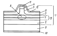
На чертеже показан предлагаемый лазер. The drawing shows the proposed laser.
Лазер содержит гетероэпитаксиальную четырехслойную структуру 1, эмиттеры 2 и 3, контактный слой 4, мезаполоску 5, барьерный слой 6 из ZnSe, активную область 7, диаграмму 8 излучения в плоскости p-n-перехода, подложку 9, слои 10 и 11 оптических контактов, расширенный контакт 12 и трехслойный волновод 13. The laser contains a heteroepitaxial four-
П р и м е р. В пятислойной эпитаксиальной структуре на λ 0,85 мкм составе контактный слой 4 GaAsp++. Р-эмиттер 3 Al0,6Ga0,4As, волноводный слой Al0,3Ga0,7As, активная область 7 Al0,05Ga0,95As, волноводный слой Al0,3Ga0,4As, N-эмиттер 2 Al0,6Ga0,4As. Сформирована мезаполоска 5 шириной 2,8 мкм. Толщина Р-эмиттера 3 вне мезы составила 0,05 мкм, а начало плавного расширения мезы удалено от активной области на 0,2 мкм. Мезаструктура со сформированным полосковым омическим контактом слоя 10 была заращена слоем 6 ZnSе толщиной 0,4 мкм, а после его удаления со стороны эпитаксиальных слоев напылен расширенный контакт 12.PRI me R. In the five-layer epitaxial structure at λ 0.85 μm composition, the contact layer is 4 GaAsp ++ .
Формирование сплошного контакта Au-Ge-Au производилось по стандартной технологии. Затем пластина разделялась на элементы, которые напаивались на медный теплоотвод для испытаний. The formation of a continuous contact Au-Ge-Au was carried out according to standard technology. Then the plate was divided into elements that were soldered to a copper heat sink for testing.
Измерения дали следующие результаты, существенно превосходящие параметры лазеров, описанных в прототипе:
Iпор 20-25 мА
ηэфф 60-70%
Линейность ВТАХ до 80-100 мВт
Предельная мощность до 200 мВт
Угловая расходимость излучения 10х25о
Астигматическая разность менее 5 мкм.The measurements gave the following results, significantly superior to the parameters of the lasers described in the prototype:
I then 20-25 mA
η eff 60-70%
VTAC linearity up to 80-100 mW
Ultimate power up to 200 mW
Angular divergence of radiation 10х25 о
Astigmatic difference less than 5 microns.
Проведенные экспериментальные исследования предложенного инжекционного лазера, как и показано в примере, позволили снизить пороговые токи, увеличить квантовую эффективность, улучшить линейность ватт-амперной характеристики, что позволило стабилизировать одномодовый режим регенерации при повышенных мощностях излучения (до 200 мВт в непрерывном режиме) и улучшить пространственную диаграмма излучения, приближая ее к окружности при снижении астигматизма. The experimental studies of the proposed injection laser, as shown in the example, made it possible to reduce threshold currents, increase quantum efficiency, improve the linearity of the watt-ampere characteristic, which made it possible to stabilize the single-mode regeneration mode at increased radiation powers (up to 200 mW in continuous mode) and improve the spatial radiation pattern, bringing it closer to a circle with a decrease in astigmatism.
Claims (1)
Priority Applications (1)
| Application Number | Priority Date | Filing Date | Title |
|---|---|---|---|
| RU93003840A RU2035103C1 (en) | 1993-01-26 | 1993-01-26 | Injection laser |
Applications Claiming Priority (1)
| Application Number | Priority Date | Filing Date | Title |
|---|---|---|---|
| RU93003840A RU2035103C1 (en) | 1993-01-26 | 1993-01-26 | Injection laser |
Publications (2)
| Publication Number | Publication Date |
|---|---|
| RU93003840A RU93003840A (en) | 1995-02-27 |
| RU2035103C1 true RU2035103C1 (en) | 1995-05-10 |
Family
ID=20136223
Family Applications (1)
| Application Number | Title | Priority Date | Filing Date |
|---|---|---|---|
| RU93003840A RU2035103C1 (en) | 1993-01-26 | 1993-01-26 | Injection laser |
Country Status (1)
| Country | Link |
|---|---|
| RU (1) | RU2035103C1 (en) |
Cited By (7)
| Publication number | Priority date | Publication date | Assignee | Title |
|---|---|---|---|---|
| RU2109382C1 (en) * | 1996-08-19 | 1998-04-20 | Швейкин Василий Иванович | Semiconductor laser |
| RU2110874C1 (en) * | 1996-04-24 | 1998-05-10 | Закрытое акционерное общество "Полупроводниковые приборы" | Injection semiconductor laser |
| WO2002052653A1 (en) * | 2000-12-25 | 2002-07-04 | Lev Vasilievich Kozhitov | Nonplanar semiconductor devices provided with a cylindrical closed effective layer |
| RU2230411C2 (en) * | 2002-04-16 | 2004-06-10 | Федеральное государственное унитарное предприятие "Научно-исследовательский институт "Полюс" им.М.Ф.Стельмаха | Injection laser |
| RU2230410C1 (en) * | 2002-12-23 | 2004-06-10 | Федеральное государственное унитарное предприятие "Научно-исследовательский институт "Полюс" им. М.Ф. Стельмаха | Injection laser and laser diode strip |
| RU2272344C2 (en) * | 2001-04-25 | 2006-03-20 | Фудзи Фото Фильм Ко., Лтд. | Semiconductor laser unit generating high-power radiation (alternatives) and its manufacturing process |
| RU2647565C1 (en) * | 2016-11-17 | 2018-03-16 | федеральное государственное автономное образовательное учреждение высшего образования "Санкт-Петербургский политехнический университет Петра Великого" (ФГАОУ ВО "СПбПУ") | Method of producing mesa structure of strip laser |
-
1993
- 1993-01-26 RU RU93003840A patent/RU2035103C1/en not_active IP Right Cessation
Non-Patent Citations (2)
| Title |
|---|
| 1. ЕП 0376753, кл. H 01S 3/19, 1989. * |
| 2. Appl.Phus.Lett., 1987, V.51, N12, p.877-879. * |
Cited By (7)
| Publication number | Priority date | Publication date | Assignee | Title |
|---|---|---|---|---|
| RU2110874C1 (en) * | 1996-04-24 | 1998-05-10 | Закрытое акционерное общество "Полупроводниковые приборы" | Injection semiconductor laser |
| RU2109382C1 (en) * | 1996-08-19 | 1998-04-20 | Швейкин Василий Иванович | Semiconductor laser |
| WO2002052653A1 (en) * | 2000-12-25 | 2002-07-04 | Lev Vasilievich Kozhitov | Nonplanar semiconductor devices provided with a cylindrical closed effective layer |
| RU2272344C2 (en) * | 2001-04-25 | 2006-03-20 | Фудзи Фото Фильм Ко., Лтд. | Semiconductor laser unit generating high-power radiation (alternatives) and its manufacturing process |
| RU2230411C2 (en) * | 2002-04-16 | 2004-06-10 | Федеральное государственное унитарное предприятие "Научно-исследовательский институт "Полюс" им.М.Ф.Стельмаха | Injection laser |
| RU2230410C1 (en) * | 2002-12-23 | 2004-06-10 | Федеральное государственное унитарное предприятие "Научно-исследовательский институт "Полюс" им. М.Ф. Стельмаха | Injection laser and laser diode strip |
| RU2647565C1 (en) * | 2016-11-17 | 2018-03-16 | федеральное государственное автономное образовательное учреждение высшего образования "Санкт-Петербургский политехнический университет Петра Великого" (ФГАОУ ВО "СПбПУ") | Method of producing mesa structure of strip laser |
Similar Documents
| Publication | Publication Date | Title |
|---|---|---|
| JPH10303500A (en) | High-output semiconductor laser diode | |
| RU2035103C1 (en) | Injection laser | |
| JPS60150682A (en) | Semiconductor laser element | |
| US4821278A (en) | Inverted channel substrate planar semiconductor laser | |
| US4581743A (en) | Semiconductor laser having an inverted layer in a stepped offset portion | |
| JPS58225681A (en) | semiconductor laser device | |
| JPH029468B2 (en) | ||
| JPH0671121B2 (en) | Semiconductor laser device | |
| JPS62137893A (en) | semiconductor laser | |
| JPH03203282A (en) | Semiconductor laser diode | |
| KR100277936B1 (en) | Compound semiconductor laser diode and manufacturing method thereof | |
| JP2628638B2 (en) | Semiconductor laser device | |
| JPS6257271A (en) | Semiconductor laser device | |
| JPS61214591A (en) | Semiconductor laser element | |
| JPH01125570U (en) | ||
| JP2005340576A (en) | Semiconductor laser device and method for manufacturing the same, optical disc apparatus, and optical transmission system | |
| JPS60163484A (en) | Semiconductor laser | |
| JPH02254784A (en) | semiconductor laser device | |
| JPS58110085A (en) | Buried type semiconductor laser | |
| JPH01123492A (en) | semiconductor laser equipment | |
| JPH02196489A (en) | Semiconductor laser | |
| JPS58207691A (en) | Semiconductor laser element | |
| KR950010203A (en) | Semiconductor laser diode with leakage waveguide structure | |
| JPS59205788A (en) | Semiconductor laser | |
| JPH0513888A (en) | Semiconductor light emitting device and method of manufacturing the same |
Legal Events
| Date | Code | Title | Description |
|---|---|---|---|
| MM4A | The patent is invalid due to non-payment of fees |
Effective date: 20100127 |