RU2024927C1 - Microprocessor - Google Patents

Microprocessor Download PDF

Info

Publication number
RU2024927C1
RU2024927C1 SU4878494A RU2024927C1 RU 2024927 C1 RU2024927 C1 RU 2024927C1 SU 4878494 A SU4878494 A SU 4878494A RU 2024927 C1 RU2024927 C1 RU 2024927C1
Authority
RU
Russia
Prior art keywords
input
information
output
block
unit
Prior art date
Application number
Other languages
Russian (ru)
Inventor
М.Е. Макаров
А.В. Капранов
Original Assignee
Ленинградский отраслевой научно-исследовательский институт
Priority date (The priority date is an assumption and is not a legal conclusion. Google has not performed a legal analysis and makes no representation as to the accuracy of the date listed.)
Filing date
Publication date
Application filed by Ленинградский отраслевой научно-исследовательский институт filed Critical Ленинградский отраслевой научно-исследовательский институт
Priority to SU4878494 priority Critical patent/RU2024927C1/en
Application granted granted Critical
Publication of RU2024927C1 publication Critical patent/RU2024927C1/en

Links

Images

Landscapes

  • Executing Machine-Instructions (AREA)

Abstract

FIELD: computer technique. SUBSTANCE: microprocessor, having a special architecture, is designed for performing high-level language orders, one order for one cycle. The microprocessor may be used for decision of tasks of processing signals and images; it is provided by resources for decision of tasks of real-time control operations. The microprocessor includes three units for input-output; order forming unit; two unit of address indicators, arithmetical-logical unit, unit for memorizing parameter stack; unit for memorizing return stack, a timer and interruption controller. EFFECT: enhanced efficiency due to sustaining flow-type access of peripheral devices to a main memory unit. 1 cl, 1 dwg

Description

Предлагаемый микропроцессор (МП) имеет специальную архитектуру и предназначен для выполнения команд языка высокого уровня, одна команда за один такт. The proposed microprocessor (MP) has a special architecture and is designed to execute high level language commands, one command per cycle.

Используется в вычислительной технике - для решения задач управления в реальном времени (встраиваемое оборудование, станки с числовым программным управлением, робототехника, бортовая аппаратура, электронные АТС). It is used in computer technology to solve real-time control tasks (built-in equipment, numerically controlled machines, robotics, on-board equipment, electronic automatic telephone exchanges).

Цель изобретения - повышение производительности. The purpose of the invention is to increase productivity.

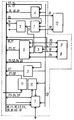
На чертеже приведена структурная схема предлагаемого микропроцессора. The drawing shows a structural diagram of the proposed microprocessor.

Микропроцессор содержит первый блок 1 ввода-вывода, блок 2 формирования команд, блок 3 указателя адреса, блок 4 указателя адреса, арифметико-логический блок 5, второй блок 6 ввода-вывода, третий блок 7 ввода-вывода, блок 8 памяти стека параметров, блоки 9 памяти стека возвратов, таймер 10 и контроллер 11 прерываний. The microprocessor comprises a first input / output unit 1, an instruction generation unit 2, an address indicator unit 3, an address indicator unit 4, an arithmetic logic unit 5, a second input / output unit 6, a third input / output unit 7, a parameter stack memory unit 8, blocks 9 memory stack returns, timer 10 and controller 11 interrupts.

Далее в состав микропроцессора входит магистраль 13, объединяющая информационные шины (далее шины):
- 14 литерала, 15 короткого литерала, 16 адреса памяти стека параметров и 17 памяти стека возвратов, 18 счетчика команд, 19 пользовательского сегментного регистра, 20 регистров сегментов данных и программ, 21 результата вычислений, 22 второго элемента стека параметров, 23 первого элемента стека возвратов, 24 внутренних источников, 25 поддержки деления/умножения и 26 квадратного корня, 27 вектора, 28 регистра маски, информационная шина 29 верхнего элемента стека параметров, вход-выход 30, выход 31, выход 32, входы-выходы 33, 34, 35, выход 36.
Next, the microprocessor includes line 13, which combines information buses (hereinafter referred to as tires):
- 14 literals, 15 short literals, 16 memory addresses of the parameter stack and 17 memory of the return stack, 18 instruction counter, 19 user segment register, 20 data and program segment registers, 21 calculation results, 22 second element of the parameter stack, 23 first element of the return stack , 24 internal sources, 25 support for division / multiplication and 26 square roots, 27 vectors, 28 mask registers, information bus 29 of the upper element of the parameter stack, input-output 30, output 31, output 32, input-outputs 33, 34, 35, exit 36.

Блок 4 формирует и по шине передает адрес к блоку 12. После формирования адреса и передачи его к блоку 12 команды или данные поступают в блок 1 по входу-выходу 30. Команды по шине поступают в регистр, содержащийся в блоке 2. Команды дешифрируются блоком 2 и подаются к блокам микропроцессора для управления информационным потоком. Микропроцессор принимает внешний сигнал синхронизации и формирует внутренний сигнал синхронизации (ССК) для кодирования и фиксации. Команда фиксируется в блоке 2 положительным фронтом CLK и декодируется во время верхнего состояния CLK. Декодирование завершается до перехода к нижнему состоянию. До прихода следующего положительного фронта CLK происходит определение ячейки памяти в блоке 12 (содержащей следующую команду или информационное слово) и выполнение микропроцессором текущей команды. Другими словами, происходит совмещение двух основных действий микропроцессора, формирование (следующего) адреса и выполнение уже принятой команды. Block 4 generates and transmits the address to block 12 via the bus. After the address is generated and transmitted to block 12, the commands or data are sent to block 1 via input / output 30. The commands are sent to the register contained in block 2 via the bus. Commands are decrypted by block 2 and fed to the microprocessor units to control the information flow. The microprocessor receives an external synchronization signal and generates an internal synchronization signal (CCK) for encoding and fixing. The command is locked in block 2 by the positive edge of CLK and is decoded during the upper state of CLK. Decoding ends before the transition to the lower state. Before the next positive edge CLK arrives, the memory cell is determined in block 12 (containing the next command or information word) and the microprocessor executes the current command. In other words, the two main actions of the microprocessor are combined, the formation of the (next) address and the execution of an already accepted command.

Далее информация по шине подается на вход блока 6 и может быть помещена в регистр, являющийся вторым элементом стека параметров, первым (верхним) элементом является регистр в блоке 5. Further, information on the bus is fed to the input of block 6 and can be placed in the register, which is the second element of the parameter stack, the first (upper) element is the register in block 5.

В свою очередь, блок 6 соединен шиной с блоком 5 и другой шиной с блоком. Связь регистра, входящего в блок 6 с блоком 9, осуществляется соответствующей шиной. Информация, извлекаемая из блока 8 и блока 9 по адресам, формируется блоком 3. In turn, block 6 is connected by a bus to block 5 and another bus to the block. The communication of the register included in block 6 with block 9 is carried out by the corresponding bus. Information extracted from block 8 and block 9 at addresses is generated by block 3.

Через блок 6 может осуществляться обмен содержимым блоков 9 и 8. Информация, содержащаяся в блоках 8, 9, через блок 6 подается в одном случае по шине на входы блока 5 и блока 1, в другом случае - по шине на вход блока 4 и используется им для формирования адресов возврата при вызове подпрограмм. Through the block 6, the contents of the blocks 9 and 8 can be exchanged. The information contained in the blocks 8, 9 is transmitted through the block 6 in one case via the bus to the inputs of the block 5 and block 1, in the other case - via the bus to the input of the block 4 them to generate return addresses when calling routines.

Блок 5 преобразовывает информацию и передает ее по шине на входы блоков 4, 3, 1, 6 и 7. Блок 7 используется для расширения возможностей ввода-вывода. Block 5 converts the information and transfers it over the bus to the inputs of blocks 4, 3, 1, 6, and 7. Block 7 is used to expand the capabilities of I / O.

Claims (1)

МИКРОПРОЦЕССОР, содержащий первый, второй и третий блоки ввода-вывода, блок формирования команд, первый и второй блоки указателя, арифметико-логический блок, блок памяти стека параметров, блок памяти стека возвратов, таймер и контроллер прерываний, причем управляющие входы первого, второго и третьего блоков ввода-вывода, первого и второго блоков указателя адреса, арифметико-логического блока, блока памяти стека параметров, блока памяти стека возвратов, таймера и контроллера прерываний соединены с соответствующими выходами первой группы блока формирования команд, тактовый вход и вход пуска которого подключены соответственно к одноименным входам микропроцессора, первый информационный вход-выход которого подключен к первым информационным входам первого и третьего блоков ввода-вывода таймера, второго блока указателя адреса, информационному входу второго блока указателя адреса и информационному входу-выходу арифметико-логического блока, информационный выход которого соединен с первым информационным входом первой группы второго блока ввода-вывода, вторая группа информационных входов которого соединена с группой информационных входов блока формирования команд и группой информационных выходов первого блока ввода-вывода, второй информационный вход которого соединен с первым информационным выходом второго блока ввода-вывода, первый и второй информационные входы-выходы которого соединены с информационными входами-выходами соответственно блока памяти стека параметров и блока памяти стека возвратов, адресные входы которых соединены соответственно с первым и вторым выходами первого блока указателя адреса, информационный вход-выход первого блока ввода-вывода является вторым информационным входом-выходом микропроцессора, адресный выход которого подключен к первому выходу второго блока указателя адреса, второй выход которого соединен с вторым информационным входом первой группы второго блока ввода-вывода, второй информационный выход которого соединен с первым информационным входом группы второго блока указателя адреса, второй информационный вход группы которого соединен с выходом вектора прерываний контроллера прерываний, вход прерываний которого является одноименным входом микропроцессора, первый, второй и третий информационные выходы группы третьего блока ввода-вывода и первый информационный выход второго блока ввода-вывода соединены с соответствующими информационными входами группы арифметико-логического блока, второй, третий и четвертый информационные выходы второго блока указателя адреса, первый и второй выходы первого блока указателя адреса, первый и второй информационные выходы второго блока ввода-вывода и выход прерываний контроллера прерываний соединены с соответствующими информационными входами первой группы третьего блока ввода-вывода, информационный вход-выход которого является третьим информационным входом-выходом микропроцессора, информационный выход третьего блока ввода-вывода соединен с вторым информационным входом таймера, отличающийся тем, что, с целью повышения производительности, группа выходов таймера соединена с второй группой информационных входов третьего блока ввода-вывода. The microprocessor containing the first, second and third input-output blocks, a command generation block, the first and second pointer blocks, an arithmetic-logical block, a parameter stack memory block, a return stack memory block, a timer and an interrupt controller, the control inputs of the first, second and the third I / O blocks, the first and second blocks of the address pointer, the arithmetic logic block, the memory block of the parameter stack, the memory block of the return stack, timer, and interrupt controller are connected to the corresponding outputs of the first group a command generation unit whose clock input and start input are connected respectively to the inputs of the same microprocessor, the first information input-output of which is connected to the first information inputs of the first and third timer I / O blocks, the second address pointer block, the information input of the second address pointer block and the information the input-output of the arithmetic-logical unit, the information output of which is connected to the first information input of the first group of the second input-output unit, the second group of information the input inputs of which are connected to the group of information inputs of the command generation unit and the group of information outputs of the first input-output unit, the second information input of which is connected to the first information output of the second input-output unit, the first and second information inputs-outputs of which are connected to information inputs and outputs respectively, the memory block of the stack of parameters and the memory block of the stack of returns, the address inputs of which are connected respectively with the first and second outputs of the first block of the pointer a Resa, the information input-output of the first input-output unit is the second information input-output of the microprocessor, the address output of which is connected to the first output of the second unit of the address indicator, the second output of which is connected to the second information input of the first group of the second input-output unit, the second information output which is connected to the first information input of the group of the second block of the address pointer, the second information input of the group of which is connected to the output of the interrupt vector of the interrupt controller, the input interruptions of which is the microprocessor input of the same name, the first, second and third information outputs of the group of the third input-output unit and the first information output of the second input-output unit are connected to the corresponding information inputs of the arithmetic-logical unit group, the second, third and fourth information outputs of the second pointer block addresses, the first and second outputs of the first block of the address pointer, the first and second information outputs of the second I / O block and the interrupt output of the interrupt controller connected to the corresponding information inputs of the first group of the third input-output unit, the information input-output of which is the third information input-output of the microprocessor, the information output of the third input-output unit is connected to the second information input of the timer, characterized in that, in order to increase productivity, the group of timer outputs is connected to the second group of information inputs of the third input-output block.
SU4878494 1990-10-29 1990-10-29 Microprocessor RU2024927C1 (en)

Priority Applications (1)

Application Number Priority Date Filing Date Title
SU4878494 RU2024927C1 (en) 1990-10-29 1990-10-29 Microprocessor

Applications Claiming Priority (1)

Application Number Priority Date Filing Date Title
SU4878494 RU2024927C1 (en) 1990-10-29 1990-10-29 Microprocessor

Publications (1)

Publication Number Publication Date
RU2024927C1 true RU2024927C1 (en) 1994-12-15

Family

ID=21542962

Family Applications (1)

Application Number Title Priority Date Filing Date
SU4878494 RU2024927C1 (en) 1990-10-29 1990-10-29 Microprocessor

Country Status (1)

Country Link
RU (1) RU2024927C1 (en)

Non-Patent Citations (1)

* Cited by examiner, † Cited by third party
Title
Electronic engineering, 01.89, ном.745, р.56,58. *

Similar Documents

Publication Publication Date Title
US4748559A (en) Apparatus for reducing power consumed by a static microprocessor
US4758945A (en) Method for reducing power consumed by a static microprocessor
US4112490A (en) Data transfer control apparatus and method
EP0368144B1 (en) Digital computing system with low power mode
US3886523A (en) Micro program data processor having parallel instruction flow streams for plural levels of sub instruction sets
US4307447A (en) Programmable controller
US4484303A (en) Programmable controller
EP0511674A2 (en) Single chip microcomputer
US4266270A (en) Microprocessor having plural internal data buses
JPS5841538B2 (en) Multiprocessor system instructions
EP0498595B1 (en) Single chip digital processor and method for operating it
JPH08212100A (en) Emulation chip for single-chip microcomputer
Mazur et al. PLC implementation in the form of a System-on-a-Chip
JPS62115542A (en) Information processor
JPH10161871A (en) Processor
RU2024927C1 (en) Microprocessor
US4451882A (en) Data processing system
US4409653A (en) Method of performing a clear and wait operation with a single instruction
CA1137641A (en) Single chip microcomputer selectively operable in response to instructions stored on the computer chip or in response to instructions stored external to the chip
JP2826309B2 (en) Information processing device
JP3116444B2 (en) Semiconductor computing equipment and electronic equipment
KR100240658B1 (en) Hierarchical controller and interrupt management circuit for high-level synthesis
JPS63155330A (en) Microprogram controller
GB2027238A (en) Clear and wait instruction means and method
SU435527A1 (en) PROCESSOR TO CONTROL DIGITAL CIRCUITS