RU107419U1 - IGBT DRIVER - Google Patents
IGBT DRIVER Download PDFInfo
- Publication number
- RU107419U1 RU107419U1 RU2011107044/07U RU2011107044U RU107419U1 RU 107419 U1 RU107419 U1 RU 107419U1 RU 2011107044/07 U RU2011107044/07 U RU 2011107044/07U RU 2011107044 U RU2011107044 U RU 2011107044U RU 107419 U1 RU107419 U1 RU 107419U1
- Authority
- RU
- Russia
- Prior art keywords
- output
- voltage
- driver
- igbt
- transistors
- Prior art date
Links
Landscapes
- Amplifiers (AREA)
- Electronic Switches (AREA)
Abstract
Драйвер IGBT, содержащий входную гальванически развязанную цепь управления, промежуточный усилитель и выходные формирователи токов затвора IGBT, отличающийся тем, что в него введен симметричный усилитель напряжения на встречных источниках тока, интегрирующий конденсатор, нормирующий скорость изменения выходного напряжения, двухтактный эмиттерный повторитель на выходе, втекающий и вытекающий токи которого ограничены резисторами в эмиттерах транзисторов, и диоды Шоттки, ограничивающие амплитуды наведенных импульсов напряжения на выходе драйвера на уровнях питающих напряжений драйвера. An IGBT driver containing an input galvanically isolated control circuit, an intermediate amplifier, and output gate current conditioners IGBT, characterized in that a symmetrical voltage amplifier is introduced into the oncoming current sources, an integrating capacitor, normalizing the rate of change of the output voltage, a push-pull emitter repeater at the output, flowing in and leakage currents of which are limited by resistors in the emitters of transistors, and Schottky diodes, limiting the amplitudes of the induced voltage pulses at the output drivers at driver voltage levels.
Description
Полезная модель относится к электротехнике, в частности, к преобразовательной технике, и может быть использована как драйвер IGBT.The utility model relates to electrical engineering, in particular, to converter technology, and can be used as an IGBT driver.
Известны схемы драйверов [1], в состав которых входят оптопара, усилитель напряжения на транзисторе с резистором в качестве нагрузки, и двухтактный эмиттерный повторитель (Фиг.1).Known driver circuits [1], which include an optocoupler, a voltage amplifier on a transistor with a resistor as a load, and a push-pull emitter follower (Figure 1).
Недостатки таких схем: несимметричная работа усилителя при высоком и низком уровне импульса напряжения, ненормированная скорость изменения напряжения при нарастании и спаде импульса, отсутствие ограничения амплитуды импульса тока на выходе драйвера, возможность наведенных импульсов напряжения на выход драйвера, опасных для затвора IGBT.The disadvantages of such schemes are asymmetric operation of the amplifier at a high and low voltage pulse level, the abnormal rate of voltage change during rise and fall of the pulse, the lack of limitation of the amplitude of the current pulse at the driver output, the possibility of induced voltage pulses at the driver output, which are dangerous for the IGBT gate.
Задачи полезной модели: симметрировать усилитель, нормировать скорость изменения напряжения, ограничить амплитуду импульса выходного тока, ограничить амплитуду наведенных импульсов напряжения на выходе драйвера на безопасном уровне.Objectives of the utility model: to balance the amplifier, normalize the rate of change of voltage, limit the amplitude of the output current pulse, limit the amplitude of the induced voltage pulses at the driver output to a safe level.
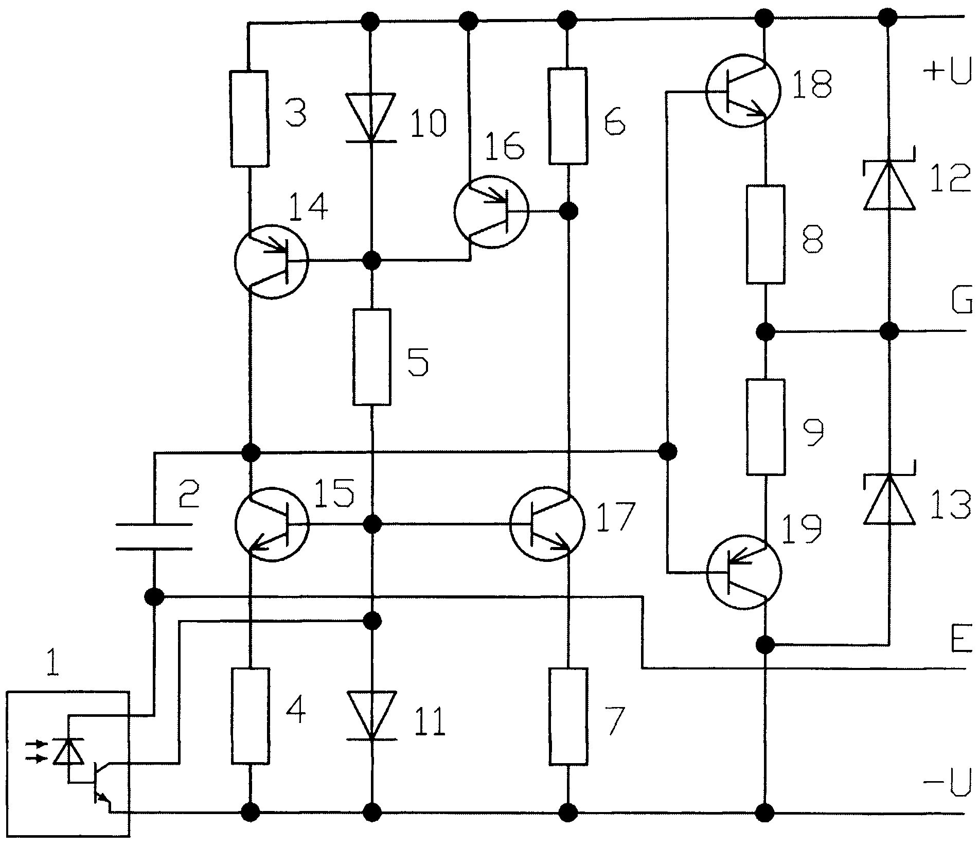
На Фиг.2 представлена схема предлагаемого драйвера.Figure 2 presents a diagram of the proposed driver.
Драйвер содержит оптопару или оптоприемник 1, конденсатор 2, резисторы 3…9, стабисторы 10 и 11, диоды Шоттки 12 и 13, транзисторы 14…19.The driver contains an optocoupler or an optical receiver 1, a capacitor 2, resistors 3 ... 9, resistors 10 and 11, Schottky diodes 12 and 13, transistors 14 ... 19.
Драйвер работает следующим образом:The driver works as follows:
Ток, протекающий через резистор 5 и стабисторы 10, 11, создает на базах транзисторов 14 и 15 отпирающие напряжения. Благодаря резисторам 3 и 4, соединенным с эмиттерами и источниками питающих напряжений +U и -U, коллекторные токи транзисторов стабилизированы, то есть получаются встречные источники тока. Состояния транзисторов переключаются оптоприемником 1 и вспомогательными транзисторами 16 и 17. В исходном режиме транзистор оптоприемника заперт, транзисторы 15, 17 и 16 включены, а транзистор 14 выключен. На выходе драйвера G напряжение отрицательно относительно вывода Е. При подаче управляющего импульса на оптоприемник 1 его транзистор включается, при этом выключаются транзисторы 15, 17, 16, а транзистор 14 включается. Происходит заряд конденсатора 2 стабильным током практически до уровня напряжения +U, то есть конденсатор выполняет функцию интегратора. Напряжение на базах транзисторов 18, 19 эмиттерного повторителя повышается по линейному закону. Выходное напряжение драйвера тоже повышается, ток транзистора 18 (вытекающий) ограничивается резистором 8. После окончания управляющего импульса драйвер возвращается в исходный режим, конденсатор 2 разряжается стабильным током практически до уровня напряжения -U. Напряжение на базах транзисторов 18, 19 понижается по линейному закону. Выходное напряжение драйвера тоже понижается, ток транзистора 19 (втекающий) ограничивается резистором 9. Диоды 12 и 13 ограничивают амплитуду наведенных импульсов Напряжения практически на уровнях +U и -U, соответственно.The current flowing through the resistor 5 and the stabilizers 10, 11, creates on the bases of the transistors 14 and 15 unlocking voltage. Thanks to the resistors 3 and 4 connected to the emitters and power sources + U and -U, the collector currents of the transistors are stabilized, that is, counter current sources are obtained. The states of the transistors are switched by the optical receiver 1 and auxiliary transistors 16 and 17. In the initial mode, the optical transistor is locked, the transistors 15, 17 and 16 are turned on, and the transistor 14 is turned off. At the output of driver G, the voltage is negative with respect to terminal E. When a control pulse is applied to the optical detector 1, its transistor turns on, and transistors 15, 17, 16 turn off, and transistor 14 turns on. The capacitor 2 is charged with a stable current almost to the voltage level + U, that is, the capacitor performs the function of an integrator. The voltage at the bases of transistors 18, 19 of the emitter follower increases linearly. The output voltage of the driver also rises, the current of the transistor 18 (leaky) is limited by the resistor 8. After the end of the control pulse, the driver returns to its original mode, the capacitor 2 is discharged with a stable current almost to the voltage level -U. The voltage at the bases of transistors 18, 19 decreases linearly. The output voltage of the driver also decreases, the current of the transistor 19 (flowing) is limited by a resistor 9. Diodes 12 and 13 limit the amplitude of the induced voltage pulses almost at the levels + U and -U, respectively.
Таким образом, предложенный драйвер имеет симметричный усилитель для низкого и высокого уровней напряжения, постоянные скорости нарастания и спада напряжения, независимые уровни ограничения амплитуды вытекающего и втекающего токов, ограничивает амплитуды наведенных импульсов напряжения на выходе драйвера на безопасных уровнях.Thus, the proposed driver has a symmetric amplifier for low and high voltage levels, constant voltage rise and fall rates, independent levels of limiting the amplitude of the outgoing and incoming currents, limits the amplitudes of the induced voltage pulses at the driver output to safe levels.
Источники информации:Information sources:
1. Силовые приборы Mitsubishi - Гибридные схемы драйверов для IGBT 1. Power Mitsubishi - Hybrid driver circuits for IGBT
Claims (1)
Priority Applications (1)
| Application Number | Priority Date | Filing Date | Title |
|---|---|---|---|
| RU2011107044/07U RU107419U1 (en) | 2011-02-24 | 2011-02-24 | IGBT DRIVER |
Applications Claiming Priority (1)
| Application Number | Priority Date | Filing Date | Title |
|---|---|---|---|
| RU2011107044/07U RU107419U1 (en) | 2011-02-24 | 2011-02-24 | IGBT DRIVER |
Publications (1)
| Publication Number | Publication Date |
|---|---|
| RU107419U1 true RU107419U1 (en) | 2011-08-10 |
Family
ID=44755213
Family Applications (1)
| Application Number | Title | Priority Date | Filing Date |
|---|---|---|---|
| RU2011107044/07U RU107419U1 (en) | 2011-02-24 | 2011-02-24 | IGBT DRIVER |
Country Status (1)
| Country | Link |
|---|---|
| RU (1) | RU107419U1 (en) |
Cited By (4)
| Publication number | Priority date | Publication date | Assignee | Title |
|---|---|---|---|---|
| RU2515543C1 (en) * | 2013-04-30 | 2014-05-10 | Федеральное государственное бюджетное образовательное учреждение высшего профессионального образования "Южно-Российский государственный университет экономики и сервиса" (ФГБОУ ВПО "ЮРГУЭС") | High-speed differential link driver |
| RU2538324C2 (en) * | 2013-04-23 | 2015-01-10 | Федеральное государственное бюджетное образовательное учреждение высшего профессионального образования "Южно-Российский государственный университет экономики и серсиса" (ФГБОУ ВПО "ЮРГУЭС") | High-speed capacitive load driver |
| CN104901666A (en) * | 2015-05-20 | 2015-09-09 | 广州金升阳科技有限公司 | IGBT driving protection circuit, driver chip with circuit and protection circuit for chip |
| RU2771861C1 (en) * | 2021-10-07 | 2022-05-13 | Российская Федерация, от имени которой выступает Государственная корпорация по атомной энергии "Росатом" (Госкорпорация "Росатом") | Power transistor control driver with increased immunity |
-
2011
- 2011-02-24 RU RU2011107044/07U patent/RU107419U1/en active
Cited By (5)
| Publication number | Priority date | Publication date | Assignee | Title |
|---|---|---|---|---|
| RU2538324C2 (en) * | 2013-04-23 | 2015-01-10 | Федеральное государственное бюджетное образовательное учреждение высшего профессионального образования "Южно-Российский государственный университет экономики и серсиса" (ФГБОУ ВПО "ЮРГУЭС") | High-speed capacitive load driver |
| RU2515543C1 (en) * | 2013-04-30 | 2014-05-10 | Федеральное государственное бюджетное образовательное учреждение высшего профессионального образования "Южно-Российский государственный университет экономики и сервиса" (ФГБОУ ВПО "ЮРГУЭС") | High-speed differential link driver |
| CN104901666A (en) * | 2015-05-20 | 2015-09-09 | 广州金升阳科技有限公司 | IGBT driving protection circuit, driver chip with circuit and protection circuit for chip |
| CN104901666B (en) * | 2015-05-20 | 2017-11-24 | 广州金升阳科技有限公司 | A kind of IGBT Drive Protecting Circuits, the protection circuit using the driving chip of the circuit and the chip |
| RU2771861C1 (en) * | 2021-10-07 | 2022-05-13 | Российская Федерация, от имени которой выступает Государственная корпорация по атомной энергии "Росатом" (Госкорпорация "Росатом") | Power transistor control driver with increased immunity |
Similar Documents
| Publication | Publication Date | Title |
|---|---|---|
| US9401705B2 (en) | Gate driving device | |
| EP2991227B1 (en) | Driving device and switching circuit control method | |
| US20140035541A1 (en) | Control circuit, control method used in pfc circuit and power source system thereof | |
| US8933647B2 (en) | LED controller with current-ripple control | |
| US9571088B2 (en) | Semiconductor device | |
| CN103329412A (en) | Apparatus for driving semiconductor switch element | |
| US20190394845A1 (en) | Current Source Circuit and LED Driving Circuit | |
| TW200933329A (en) | Switching voltage regulator and the control circuit and method thereof | |
| RU107419U1 (en) | IGBT DRIVER | |
| CN107666243B (en) | Self-excitation synchronous rectification power supply circuit | |
| CN104540292A (en) | Dimming circuit applicable to silicon-controlled light regulator circuit and dimming system | |
| CN105706367A (en) | Semiconductor device | |
| US9762147B2 (en) | Power conversion system | |
| CN108021168B (en) | A kind of variable-frequency variable-voltage modulation circuit suitable for switching capacity voltage-stablizer | |
| CN104185345B (en) | A kind of control device for constant current driver circuit for LED | |
| CN105916239A (en) | Over-voltage adaptive regulation circuit for linear constant current driven LED | |
| CN211930938U (en) | LED drive circuit with high power factor and low harmonic and LED device | |
| CN203761250U (en) | Power square wave generation circuit with adjustable pulse width | |
| CN102916585B (en) | Sampling hold circuit in flyback converter | |
| CN102710130B (en) | A kind of high-precision A C/DC converter current-limiting circuits | |
| US9059594B2 (en) | Battery switching charger and method for controlling battery switching charger | |
| CN105515360A (en) | Short-circuit protection circuit based on double operational amplifiers | |
| CN108738192B (en) | Light modulation circuit | |
| RU12308U1 (en) | Optoelectronic relay | |
| US9431925B2 (en) | Half bridge circuit, full bridge circuit constructed with half bridge circuit, and three-phase inverter circuit constructed with half bridge circuit |