NL1036189A1 - Methods and System for Lithography Process Window Simulation. - Google Patents
Methods and System for Lithography Process Window Simulation. Download PDFInfo
- Publication number
- NL1036189A1 NL1036189A1 NL1036189A NL1036189A NL1036189A1 NL 1036189 A1 NL1036189 A1 NL 1036189A1 NL 1036189 A NL1036189 A NL 1036189A NL 1036189 A NL1036189 A NL 1036189A NL 1036189 A1 NL1036189 A1 NL 1036189A1
- Authority
- NL
- Netherlands
- Prior art keywords
- image
- resist
- focus
- mask
- model
- Prior art date
Links
Classifications
-
- G—PHYSICS
- G06—COMPUTING OR CALCULATING; COUNTING
- G06F—ELECTRIC DIGITAL DATA PROCESSING
- G06F30/00—Computer-aided design [CAD]
- G06F30/20—Design optimisation, verification or simulation
-
- G—PHYSICS
- G03—PHOTOGRAPHY; CINEMATOGRAPHY; ANALOGOUS TECHNIQUES USING WAVES OTHER THAN OPTICAL WAVES; ELECTROGRAPHY; HOLOGRAPHY
- G03F—PHOTOMECHANICAL PRODUCTION OF TEXTURED OR PATTERNED SURFACES, e.g. FOR PRINTING, FOR PROCESSING OF SEMICONDUCTOR DEVICES; MATERIALS THEREFOR; ORIGINALS THEREFOR; APPARATUS SPECIALLY ADAPTED THEREFOR
- G03F7/00—Photomechanical, e.g. photolithographic, production of textured or patterned surfaces, e.g. printing surfaces; Materials therefor, e.g. comprising photoresists; Apparatus specially adapted therefor
- G03F7/70—Microphotolithographic exposure; Apparatus therefor
- G03F7/70483—Information management; Active and passive control; Testing; Wafer monitoring, e.g. pattern monitoring
- G03F7/70491—Information management, e.g. software; Active and passive control, e.g. details of controlling exposure processes or exposure tool monitoring processes
- G03F7/705—Modelling or simulating from physical phenomena up to complete wafer processes or whole workflow in wafer productions
-
- G—PHYSICS
- G03—PHOTOGRAPHY; CINEMATOGRAPHY; ANALOGOUS TECHNIQUES USING WAVES OTHER THAN OPTICAL WAVES; ELECTROGRAPHY; HOLOGRAPHY
- G03F—PHOTOMECHANICAL PRODUCTION OF TEXTURED OR PATTERNED SURFACES, e.g. FOR PRINTING, FOR PROCESSING OF SEMICONDUCTOR DEVICES; MATERIALS THEREFOR; ORIGINALS THEREFOR; APPARATUS SPECIALLY ADAPTED THEREFOR
- G03F7/00—Photomechanical, e.g. photolithographic, production of textured or patterned surfaces, e.g. printing surfaces; Materials therefor, e.g. comprising photoresists; Apparatus specially adapted therefor
- G03F7/70—Microphotolithographic exposure; Apparatus therefor
- G03F7/70483—Information management; Active and passive control; Testing; Wafer monitoring, e.g. pattern monitoring
- G03F7/7055—Exposure light control in all parts of the microlithographic apparatus, e.g. pulse length control or light interruption
-
- G—PHYSICS
- G03—PHOTOGRAPHY; CINEMATOGRAPHY; ANALOGOUS TECHNIQUES USING WAVES OTHER THAN OPTICAL WAVES; ELECTROGRAPHY; HOLOGRAPHY
- G03F—PHOTOMECHANICAL PRODUCTION OF TEXTURED OR PATTERNED SURFACES, e.g. FOR PRINTING, FOR PROCESSING OF SEMICONDUCTOR DEVICES; MATERIALS THEREFOR; ORIGINALS THEREFOR; APPARATUS SPECIALLY ADAPTED THEREFOR
- G03F7/00—Photomechanical, e.g. photolithographic, production of textured or patterned surfaces, e.g. printing surfaces; Materials therefor, e.g. comprising photoresists; Apparatus specially adapted therefor
- G03F7/70—Microphotolithographic exposure; Apparatus therefor
- G03F7/708—Construction of apparatus, e.g. environment aspects, hygiene aspects or materials
- G03F7/70991—Connection with other apparatus, e.g. multiple exposure stations, particular arrangement of exposure apparatus and pre-exposure and/or post-exposure apparatus; Shared apparatus, e.g. having shared radiation source, shared mask or workpiece stage, shared base-plate; Utilities, e.g. cable, pipe or wireless arrangements for data, power, fluids or vacuum
Landscapes
- Engineering & Computer Science (AREA)
- Physics & Mathematics (AREA)
- General Physics & Mathematics (AREA)
- Theoretical Computer Science (AREA)
- Health & Medical Sciences (AREA)
- Computer Networks & Wireless Communication (AREA)
- Environmental & Geological Engineering (AREA)
- Epidemiology (AREA)
- Public Health (AREA)
- General Engineering & Computer Science (AREA)
- Geometry (AREA)
- Evolutionary Computation (AREA)
- Computer Hardware Design (AREA)
- Exposure And Positioning Against Photoresist Photosensitive Materials (AREA)
- Exposure Of Semiconductors, Excluding Electron Or Ion Beam Exposure (AREA)
Abstract
Description
Methods and System for Lithography Process Window Simulation Technical Field [001] The technical field of the present invention relates generally to a method and program product for performing simulation of the imaging results associated with a lithography process, and more specifically to a computational efficient simulation process that accounts for parameter variations over a process window.Methods and System for Lithography Process Window Simulation Technical Field [001] The technical field of the present invention relates generally to a method and program product for performing simulation of the imaging results associated with a lithography process, and more specifically to a computational efficient simulation process that accounts for parameter variations over a process window.
Background [002] Lithographic apparatus can be used, for example, in the manufacture of integrated circuits (ICs). In such a case, the mask may contain a circuit pattern corresponding to an individual layer of the IC, and this pattern can be imaged onto a target portion (e.gr. comprising one or more dies) on a substrate (silicon wafer) that has been coated with a layer of radiation-sensitive material (resist). In general, a single wafer will contain a whole network of adjacent target portions that are successively irradiated via the projection system, one at a time. In one type of lithographic projection apparatus, each target portion is irradiated by exposing the entire mask pattern onto the target portion in one go; such an apparatus is commonly referred to as a wafer stepper. In an alternative apparatus, commonly referred to as a step-and-scan apparatus, each target portion is irradiated by progressively scanning the mask pattern under the projection beam in a given reference direction (the "scanning" direction) while synchronously scanning the substrate table parallel or anti-parallel to this direction. Since, in general, the projection system will have a magnification factor M (generally < 1), the speed V at which the substrate table is scanned will be a factor M times that at which the mask table is scanned. More information with regard to lithographic devices as described herein can be gleaned, for example, from US 6,046,792, incorporated herein by reference.Background Lithographic apparatus can be used, for example, in the manufacture of integrated circuits (ICs). In such a case, the mask may contain a circuit pattern corresponding to an individual layer of the IC, and this pattern can be imaged onto a target portion (eg including one or more dies) on a substrate (silicon wafer) that has been coated with a layer of radiation-sensitive material (resist). In general, a single wafer will contain a whole network of adjacent target portions that are successively irradiated through the projection system, one at a time. In one type of lithographic projection apparatus, each target portion is irradiated by exposing the entire mask pattern onto the target portion in one go; Such an apparatus is commonly referred to as a wafer stepper. In an alternative apparatus, commonly referred to as a step-and-scan apparatus, each target portion is irradiated by progressively scanning the mask pattern under the projection beam in a given reference direction (the "scanning" direction) while synchronously scanning the substrate table parallel or anti-parallel to this direction. Since, in general, the projection system will have a magnification factor M (generally <1), the speed V at which the substrate table is scanned will be a factor M times that at which the mask table is scanned. More information with regard to lithographic devices as described can be accepted, for example, from US 6,046,792, incorporated by reference.
[003] In a manufacturing process using a lithographic projection apparatus, a mask pattern is imaged onto a substrate that is at least partially covered by a layer of radiation-sensitive material (resist). Prior to this imaging step, the substrate may undergo various procedures, such as priming, resist coating and a soft bake. After exposure, the substrate may be subjected to other procedures, such as a post-exposure bake (PEB), development, a hard bake and measurement/inspection of the imaged features. This array of procedures is used as a basis to pattern an individual layer of a device, e.g., an 1C. Such a patterned layer may then undergo various processes such as etching, ion-implantation (doping), metallization, oxidation, chemo-mechanical polishing, etc., all intended to finish off an individual layer. If several layers are required, then the whole procedure, or a variant thereof, will have to be repeated for each new layer. Eventually, an array of devices will be present on the substrate (wafer). These devices are then separated from one another by a technique such as dicing or sawing, whence the individual devices can be mounted on a carrier, connected to pins, etc.[003] In a manufacturing process using a lithographic projection apparatus, a mask pattern is imaged onto a substrate that is at least partially covered by a layer of radiation-sensitive material (resist). Prior to this imaging step, the substrate may undergo various procedures, such as priming, resist coating and a soft bake. After exposure, the substrate may be subject to other procedures, such as a post-exposure bake (PEB), development, a hard bake and measurement / inspection of the imaged features. This array of procedures is used as a basis to pattern an individual layer or a device, e.g., an 1C. Such a patterned layer may then undergo various processes such as etching, ion implantation (doping), metallization, oxidation, chemo-mechanical polishing, etc., all intended to finish off an individual layer. If several layers are required, then the whole procedure, or a variant of that, will have to be repeated for each new layer. Eventually, an array of devices will be present on the substrate (wafer). These devices are then separated from one another by a technique such as dicing or sawing, whence the individual devices can be mounted on a carrier, connected to pins, etc.
[004] For the sake of simplicity, the projection system may hereinafter be referred to as the "lens"; however, this term should be broadly interpreted as encompassing various types of projection systems, including refractive optics, reflective optics, and catadioptric systems, for example. The radiation system may also include components operating according to any of these design types for directing, shaping or controlling the projection beam of radiation, and such components may also be referred to below, collectively or singularly, as a "lens". Further, the lithographic apparatus may be of a type having two or more substrate tables (and/or two or more mask tables). In such "multiple stage" devices the additional tables may be used in parallel, or preparatory steps may be carried out on one or more tables while one or more other tables are being used for exposures. Twin stage lithographic apparatus are described, for example, in US 5,969,441, incorporated herein by reference.For the sake of simplicity, the projection system may be referred to as the "lens"; however, this term should be broadly interpreted and compassing various types of projection systems, including refractive optics, reflective optics, and catadioptric systems, for example. The radiation system may also include components operating according to any of these design types for directing, shaping or controlling the projection beam of radiation, and such components may also be referred to below, collectively or singularly, as a "lens". Further, the lithographic apparatus may be of a type having two or more substrate tables (and / or two or more mask tables). In such "multiple stage" devices the additional tables may be used in parallel, or preparatory steps may be carried out on one or more tables while one or more other tables are being used for exposures. Twin stage lithographic apparatus are described, for example, in US 5,969,441, incorporated by reference.
[005] The photolithographic masks referred to above comprise geometric patterns corresponding to the circuit components to be integrated onto a silicon wafer. The patterns used to create such masks are generated utilizing CAD (computer-aided design) programs, this process often being referred to as EDA (electronic design automation). Most CAD programs follow a set of predetermined design rules in order to create functional masks. These rules are set by processing and design limitations. For example, design rules define the space tolerance between circuit devices (such as gates, capacitors, etc.) or interconnect lines, so as to ensure that the circuit devices or lines do not interact with one another in an undesirable way. The design rule limitations are typically referred to as "critical dimensions" (CD). A critical dimension of a circuit can be defined as the smallest width of a line or hole or the smallest space between two lines or two holes. Thus, the CD determines the overall size and density of the designed circuit.The photolithographic masks referred to above include geometric patterns corresponding to the circuit components to be integrated onto a silicon wafer. The patterns used to create such masks are generated utilizing CAD (computer-aided design) programs, this process often being referred to as EDA (electronic design automation). Most CAD programs follow a set of predetermined design rules in order to create functional masks. These rules are set by processing and design limitations. For example, design rules define the space tolerance between circuit devices (such as gates, capacitors, etc.) or interconnect lines, so as to ensure that the circuit devices or lines do not interact with one in an undesirable way. The design rule limitations are typically referred to as "critical dimensions" (CD). A critical dimension of a circuit can be defined as the smallest width of a line or hole or the smallest space between two lines or two holes. Thus, the CD according to the overall size and density of the designed circuit.
Of course, one of the goals in integrated circuit fabrication is to faithfully reproduce the original circuit design on the wafer (via the mask).Whether course, one of the goals in integrated circuit fabrication is to faithfully reproduce the original circuit design on the wafer (via the mask).
[006] As noted, microlithography is a central step in the manufacturing of semiconductor integrated circuits, where patterns formed on semiconductor wafer substrates define the functional elements of semiconductor devices, such as microprocessors, memory chips etc. Similar lithographic techniques are also used in the formation of flat panel displays, micro-electro mechanical systems (MEMS) and other devices.As noted, microlithography is a central step in the manufacturing of semiconductor integrated circuits, where patterns formed on semiconductor wafer substrates define the functional elements of semiconductor devices, such as microprocessors, memory chips, etc. Similar lithographic techniques are also used in the formation of flat panel displays, micro-electro mechanical systems (MEMS) and other devices.
[007] As semiconductor manufacturing processes continue to advance, the dimensions of circuit elements have continually been reduced while the amount of functional elements, such as transistors, per device has been steadily increasing over decades, following a trend commonly referred to as 'Moore's law*. At the current state of technology, critical layers of leading-edge devices are manufactured using optical lithographic projection systems known as scanners that project a mask image onto a substrate using illumination from a deep-ultraviolet laser light source, creating individual circuit features having dimensions well below 100nm, i.e. less than half the wavelength of the projection light.[007] As semiconductor manufacturing processes continue to advance, the dimensions of circuit elements are continually reduced while the amount of functional elements, such as transistors, per device has been steadily increasing over decades, following a trend commonly referred to as' Moore's law *. At the current state of technology, critical layers or leading-edge devices are manufactured using optical lithographic projection systems known as scanners that project a mask image onto a substrate using illumination from a deep-ultraviolet laser light source, creating individual circuit features having dimensions well below 100nm, ie less than half the wavelength of the projection light.
[008] This process, in which features with dimensions smaller than the classical resolution limit of an optical projection system are printed, is commonly known as low-ki lithography, according to the resolution formula CD = ki χ Λ/ΝΑ, where λ is the wavelength of radiation employed (currently in most cases 248nm or 193nm), NA is the numerical aperture of the projection optics, CD is the 'critical dimension' -generally the smallest feature size printed- and is an empirical resolution factor. In general, the smaller /r1t the more difficult it becomes to reproduce a pattern on the wafer that resembles the shape and dimensions planned by a circuit designer in order to achieve particular electrical functionality and performance. To; overcome these difficulties, sophisticated fine-tuning steps are applied to the projection system as well as to the mask design. These include, for example, but not limited to, optimization of NA and optical coherence settings, customized illumination schemes, use of phase shifting masks, optical proximity correction in the mask layout, or other methods generally defined as 'resolution enhancement techniques' (RET).[008] This process, in which features with dimensions narrower than the classical resolution limit of an optical projection system are printed, is commonly known as low-ki lithography, according to the resolution formula CD = ki χ Λ / ΝΑ, where λ is the wavelength of radiation employed (currently in most cases 248nm or 193nm), NA is the numerical aperture of projection optics, CD is the 'critical dimension' -generally the smallest feature size printed- and is an empirical resolution factor. In general, the narrower / smaller the more difficult it becomes to reproduce a pattern on the wafer that resembles the shape and dimensions planned by a circuit designer in order to achieve particular electrical functionality and performance. To; overcome these difficulties, sophisticated fine-tuning steps are applied to the projection system as well as the mask design. These include, for example, but not limited to, optimization of NA and optical coherence settings, customized illumination schemes, use of phase shifting masks, optical proximity correction in the mask layout, or other methods generally defined as 'resolution enhancement techniques' (RET ).
[009] As one important example, optical proximity correction (OPC, sometimes also referred to as 'optical and process correction') addresses the fact that the final size and placement of a printed feature on the wafer will not simply be a function of the size and placement of the corresponding feature on the mask. It is noted that the terms 'mask' and 'reticle' are utilized interchangeably herein. For the small feature sizes and high feature densities present on typical circuit designs, the position of a particular edge of a given feature will be influenced to a certain extent by the presence or absence of other adjacent features. These proximity effects arise from minute amounts of light coupled from one feature to another. Similarly, proximity effects may arise from diffusion and other chemical effects during post-exposure bake (PEB), resist development, and etching that generally follow lithographic exposure.[009] As one important example, optical proximity correction (OPC, sometimes also referred to as 'optical and process correction') addresses the fact that the final size and placement of a printed feature on the wafer will not simply be a function of the size and placement of the corresponding feature on the mask. It is noted that the terms "mask" and "reticle" are utilized interchangeably. For the small feature sizes and high feature densities present on typical circuit designs, the position of a particular edge or a given feature will be influenced to a certain extent by the presence or absence of other adjacent features. These proximity effects arise from minute amounts of light coupled from one feature to another. Similarly, proximity effects may arise from diffusion and other chemical effects during post-exposure bake (PEB), resist development, and etching that generally follow lithographic exposure.
[010] In order to ensure that the features are generated on a semiconductor substrate in accordance with the requirements of the given target circuit design, proximity effects need to be predicted utilizing sophisticated numerical models, and corrections or pre-distortions need to be applied to the design of the mask before successful manufacturing of high-end devices becomes possible. The article "Full-Chip Lithography Simulation and Design Analysis - How OPC Is Changing IC Design", C. Spence, Proc. SPIE, Vol. 5751, pp 1-14 (2005) provides an overview of current 'model-based' optical proximity correction processes. In a typical high-end design almost every feature edge requires some modification in order to achieve printed patterns that come sufficiently close to the target design. These modifications may include shifting or biasing of edge positions or line widths as well as application of 'assist' features that are not intended to print themselves, but will affect the properties of an associated primary feature.[010] In order to ensure that the features are generated on a semiconductor substrate in accordance with the requirements of the given target circuit design, proximity effects need to be predicted utilizing sophisticated numerical models, and corrections or pre-distortions need to be applied to the design of the mask before successful manufacturing or high-end devices becomes possible. The article "Full-Chip Lithography Simulation and Design Analysis - How OPC Is Changing IC Design", C. Spence, Proc. SPIE, Vol. 5751, pp 1-14 (2005) provides an overview of current 'model-based' optical proximity correction processes. In a typical high-end design, almost every feature edge requires some modification in order to achieve printed patterns that come sufficiently close to the target design. These modifications may include shifting or biasing or edge positions or line widths as well as application or 'assist' features that are not intended to print themselves, but will affect the properties of an associated primary feature.
[011] The application of model-based OPC to a target design requires good process models and considerable computational resources, given the many millions of features typically present in a chip design. However, applying OPC is generally not an 'exact science', but an empirical, iterative process that does not always resolve all possible weaknesses on a layout. Therefore, post-OPC designs, i.e. mask layouts after application of all pattern modifications by OPC and any other RET's, need to be verified by design inspection, i.e. intensive full-chip simulation using calibrated numerical process models, in order to minimize the possibility of design flaws being built into the manufacturing of a mask set. This is driven by the enormous cost of making high-end mask sets, which run in the multi-million dollar range, as well as by the impact on turn-around time by reworking or repairing actual masks once they have been manufactured.The application of model-based OPC to a target design requires good process models and considerable computational resources, given the many millions of features typically present in a chip design. However, applying OPC is generally not an 'exact science', but an empirical, iterative process that does not always resolve all possible weaknesses on a layout. Therefore, post-OPC designs, ie mask layouts after application or all pattern modifications by OPC and any other RETs, need to be verified by design inspection, ie intensive full-chip simulation using calibrated numerical process models, in order to minimize the possibility of design flaws being built into the manufacturing of a mask set. This is driven by the enormous cost of making high-end mask sets, which run in the multi-million dollar range, as well as by the impact on turn-around time by reworking or repairing actual masks once they have been manufactured.
[012] Both OPC and full-chip RET verification may be based on numerical modeling systems and methods as described, for example in, USP App. Ser. No. 10/815,573 and an article titled "Optimized Hardware and Software For Fast, Full Chip Simulation", by Y.Both OPC and full-chip RET verification may be based on numerical modeling systems and methods as described, for example in, USP App. Ser. No. 10 / 815,573 and an article titled "Optimized Hardware and Software For Fast, Full Chip Simulation", by Y.
Cao et al., Proc. SPIE, Vol. 5754, 405 (2005).Cao et al., Proc. SPIE, Vol. 5754, 405 (2005).
[013] While full-chip numerical simulation of the lithographic patterning process has been demonstrated at a single process condition, typically best focus and best exposure dose or best 'nominal' condition, it is well known that manufacturability of a design requires sufficient tolerance of pattern fidelity against small variations in process conditions that are unavoidable during actual manufacturing. This tolerance is commonly expressed as a process window, defined as the width and height (or 'latitude') in exposure-defocus space over which CD or edge placement variations are within a predefined margin (i.e., error tolerance), for example ±10% of the nominal line width. In practice, the actual margin requirement may differ for different feature types, depending on their function and criticality. Furthermore, the process window concept can be extended to other basis parameters in addition to or besides exposure dose and defocus.[013] While full-chip numerical simulation of the lithographic patterning process has been demonstrated at a single process condition, typically best focus and best exposure dose or best 'nominal' condition, it is well known that manufacturability of a design requires sufficient tolerance or pattern fidelity against small variations in process conditions that are unavoidable during actual manufacturing. This tolerance is commonly expressed as a process window, defined as the width and height (or 'latitude') in exposure-defocus space over which CD or edge placement variations are within a predefined margin (ie, error tolerance), for example ± 10 % of the nominal line width. In practice, the actual margin requirement may differ for different feature types, depending on their function and criticality. Furthermore, the process window concept can be extended to other basic parameters in addition to or besides exposure dose and defocus.
[014] Manufacturability of a given design generally depends on the common process window of all features in a single layer. While state-of-the-art OPC application and design inspection methods are capable of optimizing and verifying a design at nominal conditions, it has been recently observed that process-window aware OPC models will be required in order to ensure manufacturability at future process nodes due to ever-decreasing tolerances and CD requirements.[014] Manufacturability of a given design generally depends on the common process window or all features in a single layer. While state-of-the-art OPC application and design inspection methods are capable of optimizing and verifying a design at nominal conditions, it has recently been observed that process-window aware OPC models will be required in order to ensure manufacturability at future process nodes due to ever-decreasing tolerances and CD requirements.
[015] Currently, in order to map out the process window of a given design with sufficient accuracy and coverage, simulations at N parameter settings (e.g., defocus and exposure dose) are required, where N can be on the order of a dozen or more. Consequently, an A/-fold multiplication of computation time is necessary if these repeated simulations at various settings are directly incorporated into the framework of an OPC application and verification flow, which typically will involve a number of iterations of full-chip lithography simulations. However, such an increase in the computational time is prohibitive when attempting to validate and/or design a given target circuit.[015] Currently, in order to map out the process window or a given design with sufficient accuracy and coverage, simulations at N parameter settings (eg, defocus and exposure dose) are required, where N can be on the order of a boxes or more. Twice, an A / -fold multiplication or computation time is necessary if these repeated simulations at various settings are directly incorporated into the framework of an OPC application and verification flow, which typically will involve a number of iterations or full-chip lithography simulations. However, such an increase in computational time is prohibitive when attempting to validate and / or design a given target circuit.
[016] As such, there is a need for simulation methods and systems which account for variations in the process-window that can be used for OPC and RET verification, and that are more computationally efficient than such a 'brute-force' approach of repeated simulation at various conditions as is currently performed by known prior art systems.[016] As such, there is a need for simulation methods and systems which account for variations in the process window that can be used for OPC and RET verification, and that are more computationally efficient than such a 'brute-force' approach or repeated simulation at various conditions as is currently performed by known prior art systems.
[017] In addition, calibration procedures for lithography models are required that provide models being valid, robust and accurate across the process window, not only at singular, specific parameter settings.In addition, calibration procedures for lithography models are required that provide models that are valid, robust and accurate across the process window, not only at singular, specific parameter settings.
Summary [018] Accordingly, the present invention relates to a method which allows for a computation efficient technique for considering variations in the process window for use in a simulation process, and which overcomes the foregoing deficiencies of the prior art techniques.Summary [018] Considering the present invention relates to a method which allows for a computation efficient technique for considering variations in the process window for use in a simulation process, and which overcomes the foregoing deficiencies of the prior art techniques.
[019] More specifically, the present invention relates to a method of simulating imaging performance of a lithographic process utilized to image a target design having a plurality of features. The method includes the steps of determining a function for generating a simulated image, where the function accounts for process variations associated with the lithographic process; and generating the simulated image utilizing the function, where the simulated image represents the imaging result of the target design for the lithographic process. In one given embodiment, the function is defined as:[019] More specifically, the present invention relates to a method of simulating imaging performance or a lithographic process utilized to image a target design having a variety of features. The method includes the steps of determining a function for generating a simulated image, where the function accounts for process variations associated with the lithographic process; and generating the simulated image utilizing the function, where the simulated image represents the imaging result of the target design for the lithographic process. In one given embodiment, the function is defined as:

where Io represents image intensity at nominal focus, /0 represents nominal focus, ƒ represents an actual focus level at which the simulated image is calculated, and parameters "a" and "b" represent first order and second order derivative images.where Io represents image intensity at nominal focus, / 0 represents nominal focus, ƒ represents an actual focus level at which the simulated image is calculated, and parameters "a" and "b" represent first order and second order derivative images.
[020] The present invention provides significant advantages over prior art methods. Most importantly, the present invention provides a computational efficient simulation process with accounts for variations in the process window (e.g., focus variations and exposure dose variations), and eliminates the need to perform the 'brute-force' approach of repeated simulation at various conditions as is currently practiced by known prior art methods. Indeed, as further noted below, when considering N process window conditions for purposes of the simulation, the computation time of the present method is approximately 27, whereas the prior art method would require approximately NT, where 7 denotes the computation time required for simulating one process window condition.The present invention provides significant advantages over prior art methods. Most importantly, the present invention provides a computational efficient simulation process with accounts for variations in the process window (eg, focus variations and exposure dose variations), and eliminates the need to perform the 'brute-force' approach or repeated simulation at various conditions as is currently practiced by known prior art methods. Indeed, as further noted below, when considering N process window conditions for purposes of the simulation, the computation time of the present method is approximately 27, whereas the prior art method would require approximately NT, where 7 denotes the computation time required for simulating one process window condition.
[021] The method of the present invention is also readily applied to other applications such as, but not limited to, model calibration; lithography design inspection; yield estimates based on evaluation of common process windows; identification of hot spots (or problem spots) and correction of such hot-spots by utilizing process window aware OPC; and model-based process control corrections (e.g., to center the common process window for a given lithography layer in the lithography process).[021] The method of the present invention is also readily applied to other applications such as, but not limited to, model calibration; lithography design inspection; yield estimates based on evaluation or common process windows; identification of hot spots (or problem spots) and correction of such hot spots by utilizing process window aware OPC; and model-based process control corrections (e.g., to center the common process window for a given lithography layer in the lithography process).
[022] Although specific reference may be made in this text to the use of the invention in the manufacture of ICs, it should be explicitly understood that the invention has many other possible applications. For example, it may be employed in the manufacture of integrated optical systems, guidance and detection patterns for magnetic domain memories, liquid-crystal display panels, thin-film magnetic heads, etc. The skilled artisan will appreciate that, in the context of such alternative applications, any use of the terms "reticle", "wafer" or "die" in this text should be considered as being replaced by the more general terms "mask", "substrate" and "target portion", respectively.[022] Although specific reference may be made in this text to the use of the invention in the manufacture of ICs, it should be explicitly understood that the invention has many other possible applications. For example, it may be employed in the manufacture of integrated optical systems, guidance and detection patterns for magnetic domain memories, liquid-crystal display panels, thin-film magnetic heads, etc. The skilled artisan will appreciate that, in the context of such alternative applications, any use of the terms "reticle", "wafer" or "that" in this text should be considered as being replaced by the more general terms "mask", "substrate" and "target portion", respectively.
[023] In the present document, the terms "radiation" and "beam" are used to encompass all types of electromagnetic radiation, including ultraviolet radiation (e.g. with a wavelength of 365, 248,193,157 or 126 nm) and EUV (extreme ultra-violet radiation, e.g. having a wavelength in the range 5-20 nm).[023] In the present document, the terms "radiation" and "beam" are used to encompass all types of electromagnetic radiation, including ultraviolet radiation (eg with a wavelength of 365, 248,193,157 or 126 nm) and EUV (extreme ultra-violet radiation, eg having a wavelength in the range 5-20 nm).
[024] The term mask as employed in this text may be broadly interpreted as referring to generic patterning means that can be used to endow an incoming radiation beam with a patterned cross-section, corresponding to a pattern that is to be created in a target portion of the substrate; the term "light valve" can also be used in this context. Besides the classic mask (transmissive or reflective; binary, phase-shifting, hybrid, etc.), examples of other such patterning means include: • a programmable mirror array. An example of such a device is a matrix-addressable surface having a viscoelastic control layer and a reflective surface. The basic principle behind such an apparatus is that (for example) addressed areas of the reflective surface reflect incident light as diffracted light, whereas unaddressed areas reflect incident light as undiffracted light. Using an appropriate filter, the said undiffracted light can be filtered out of the reflected beam, leaving only the diffracted light behind; in this manner, the beam becomes patterned according to the addressing pattern of the matrix-addressable surface. The required matrix addressing can be performed using suitable electronic means. More information on such mirror arrays can be gleaned, for example, from United States Patents US 5,296,891 and US 5,523,193, which are incorporated herein by reference. • a programmable LCD array. An example of such a construction is given in United States Patent US 5,229,872, which is incorporated herein by reference.[024] The term mask as employed in this text may be broadly interpreted as referring to generic patterning means that can be used to endow an incoming radiation beam with a patterned cross-section, corresponding to a pattern that has been created in a target portion of the substrate; the term "light valve" can also be used in this context. Besides the classic mask (transmissive or reflective; binary, phase-shifting, hybrid, etc.), examples of other such patterning means include: • a programmable mirror array. An example of such a device is a matrix-addressable surface having a viscoelastic control layer and a reflective surface. The basic principle behind such an apparatus is that (for example) addressed areas of the reflective surface reflect incident light as diffracted light, whereas unaddressed areas reflect incident light as undiffracted light. Using an appropriate filter, the said undiffracted light can be filtered out of the reflected beam, leaving only the diffracted light behind; in this manner, the beam becomes patterned according to the addressing pattern or the matrix-addressable surface. The required matrix addressing can be performed using suitable electronic means. More information on such mirror arrays can be glazed, for example, from United States Patents US 5,296,891 and US 5,523,193, which are incorporated by reference. • a programmable LCD array. An example of such a construction is given in United States Patent US 5,229,872, which is incorporated by reference.
[025] The invention itself, together with further objects and advantages, can be better understood by reference to the following detailed description and the accompanying schematic drawings.[025] The invention itself, together with further objects and advantages, can be better understood by reference to the following detailed description and the accompanying schematic drawings.
Brief Description of the Drawings [026] Fig. 1 is an exemplary block diagram illustrating a typical lithographic projection system.Brief Description of the Drawings FIG. 1 is an exemplary block diagram illustrating a typical lithographic projection system.
[027] Fig. 2 is an exemplary block diagram illustrating the functional modules of a lithographic simulation model.FIG. 2 is an exemplary block diagram illustrating the functional modules or a lithographic simulation model.
[028] Fig. 3 illustrates an exemplary flowchart of a first embodiment of the present invention.FIG. 3 illustrates an exemplary flowchart or a first embodiment of the present invention.
[029] Fig. 4 illustrates an exemplary flowchart of a second embodiment of the present invention.FIG. 4 illustrates an exemplary flowchart or a second embodiment of the present invention.
[030] Fig. 5 illustrates an exemplary flowchart of a third embodiment of the present invention.FIG. 5 illustrates an exemplary flowchart or a third embodiment of the present invention.
[031] Fig. 6 is a block diagram that illustrates a computer system which can assist in the implementation of the simulation method of the present invention.FIG. 6 is a block diagram that illustrates a computer system which can assist in the implementation of the simulation method of the present invention.
[032] Fig. 7 schematically depicts a lithographic projection apparatus suitable for use with the method of the present invention.FIG. 7 schematically depicts a lithographic projection apparatus suitable for use with the method of the present invention.
Detailed Description [033] Prior to discussing the present invention, a brief discussion regarding the overall simulation and imaging process is provided. Fig. 1 illustrates an exemplary lithographic projection system 10. The major components are a light source 12, which may be a deep-ultraviolet excimer laser source, illumination optics which define the partial coherence (denoted as sigma) and which may include specific source shaping optics 14, 16a and 16b; a mask or reticle 18; and projection optics 16c that produce an image of the reticle pattern onto the wafer plane 22. An adjustable filter or aperture 20 at the pupil plane may restrict the range of beam angles that impinge on the wafer plane 22, where the largest possible angle defines the numerical aperture of the projection optics NA=sin(0max).Detailed Description Prior to discussing the present invention, a letter discussing the overall simulation and imaging process is provided. FIG. 1 illustrates an exemplary lithographic projection system 10. The major components are a light source 12, which may be a deep-ultraviolet excimer laser source, illumination optics which define the partial coherence (denoted as sigma) and which may include specific source shaping optics 14 , 16a and 16b; a mask or reticle 18; and projection optics 16c that produce an image of the reticle pattern on the wafer plane 22. An adjustable filter or aperture 20 at the pupil plane may restrict the range of beam angles that impinge on the wafer plane 22, where the largest possible angle defines the numerical aperture of the projection optics NA = sin (0max).
[034] In a lithography simulation system, these major system components can be described by separate functional modules, for example, as illustrated in Fig. 2. Referring to Fig. 2, the functional modules include the design layout module 26, which defines the target design; the mask layout module 28, which defines the mask to be utilized in imaging process; the mask model module 30, which defines the model of the mask layout to be utilized during the simulation process; the optical model module 32, which defines the performance of the optical components of lithography system; and the resist model module 34, which defines the performance of the resist being utilized in the given process. As is known, the result of the simulation process produces, for example, predicted contours and CDs in the result module 36.In a lithography simulation system, these major system components can be described by separate functional modules, for example, as illustrated in FIG. 2. Referring to FIG. 2, the functional modules include the design layout module 26, which defines the target design; the mask layout module 28, which defines the mask to be utilized in imaging process; the mask model module 30, which defines the model of the mask layout to be utilized during the simulation process; the optical model module 32, which defines the performance of the optical components or lithography system; and the resist model module 34, which defines the performance of the resist being utilized in the given process. As is known, the result of the simulation process produces, for example, predicted contours and CDs in the result module 36.
[035] More specifically, it is noted that the properties of the illumination and projection optics are captured in the optical model 32 that includes, but not limited to, NA-sigma (σ) settings as well as any particular illumination source shape. The optical properties of the photo-resist layer coated on a substrate - i.e. refractive index, film thickness, propagation and polarization effects- may also be captured as part of the optical model 32. The mask model 30 captures the design features of the reticle and may also include a representation of detailed physical properties of the mask, as described, for example, in USP App. No. 60/719,837. Finally, the resist model 34 describes the effects of chemical processes which occur during resist exposure, PEB and development, in order to predict, for example, contours of resist features formed on the substrate wafer. The objective of the simulation is to accurately predict, for example, edge placements and CDs, which can then be compared against the target design. The target design, is generally defined as the pre-OPC mask layout, and will be provided in a standardized digital file format such as GDSII or OASIS.[035] More specifically, it is noted that the properties of the illumination and projection optics are captured in the optical model. 32 that includes, but not limited to, NA-sigma (σ) settings as well as any particular illumination source shape. The optical properties of the photo-resist layer coated on a substrate - ie refractive index, film thickness, propagation and polarization effects - may also be captured as part of the optical model 32. The mask model 30 captures the design features of the reticle and may also include a representation of detailed physical properties of the mask, as described, for example, in USP App. No. 60 / 719,837. Finally, the resist model 34 describes the effects of chemical processes which occur during resist exposure, PEB and development, in order to predict, for example, contours of resist features formed on the substrate wafer. The objective of simulation is to accurately predicted, for example, edge placements and CDs, which can then be compared against the target design. The target design is generally defined as the pre-OPC mask layout, and will be provided in a standardized digital file format such as GDSII or OASIS.
[036] In general, the connection between the optical and the resist model is a simulated aerial image within the resist layer, which arises from the projection of light onto the substrate, refraction at the resist interface and multiple reflections in the resist film stack. The light intensity distribution (aerial image) is turned into a latent 'resist image' by absorption of photons, which is further modified by diffusion processes and various loading effects. Efficient simulation methods that are fast enough for full-chip applications approximate the realistic 3-dimensional intensity distribution in the resist stack by a 2-dimensional aerial (and resist) image. An efficient implementation of a lithography model is possible using the following formalism, where the image (here in scalar form, which may be extended to include polarization vector effects) is expressed as a Fourier sum over signal amplitudes in the pupil plane. According to the standard Hopkins theory, the aerial image may be defined by:[036] In general, the connection between the optical and the resist model is a simulated aerial image within the resist layer, which arises from the projection of light onto the substrate, refraction at the resist interface and multiple reflections in the resist film stack. The light intensity distribution (aerial image) has turned into a latent 'resist image' by absorption or photons, which is further modified by diffusion processes and various loading effects. Efficient simulation methods that are fast enough for full-chip applications approximate the realistic 3-dimensional intensity distribution in the resist stack by a 2-dimensional aerial (and resist) image. An efficient implementation of a lithography model is possible using the following formalism, where the image (here in scalar form, which may be extended to include polarization vector effects) is expressed as a Fourier sum about signal amplitudes in the pupil plane. According to the standard Hopkins theory, the aerial image may be defined by:

(Eq.1) where, ƒ (x) is the aerial image intensity at point x within the image plane (for notational simplicity, a two-dimensional coordinate represented by a single variable is utilized), A represents a point on the source plane, A (k) is the source amplitude from point k, k' and A" are points on the pupil plane, M is the Fourier transform of the mask image, P is the pupil function, and TCCk,r = ^ A(k)2 P(k + k') P\k + A"). An important aspect of the foregoing derivation is the change of summation order (moving the sum over k inside) and indices (replacing A:'with A+A' and replacing A" with A+ A"), which results in the separation of the Transmission Cross Coefficients (TCCs), defined by the term inside the square brackets in the third line in the equation. These coefficients are independent of the mask pattern and therefore can be pre-computed using knowledge of the optical elements or configuration only (e.g., NA and σ or the detailed illuminator profile). It is further noted that although in the given example (Eq.1) is derived from a scalar imaging model, this formalism can also be extended to a vector imaging model, where TE and TM polarized light components are summed separately.(Eq.1) where, ƒ (x) is the aerial image intensity at point x within the image plane (for notational simplicity, a two-dimensional coordinate represented by a single variable is utilized), A represents a point on the source plane , A (k) is the source amplitude from point k, k 'and A "are points on the pupil plane, M is the Fourier transform or the mask image, P is the pupil function, and TCCk, r = ^ A (k ) 2 P (k + k ') P \ k + A "). An important aspect of the foregoing derivation is the change of summation order (moving the sum over k inside) and indices (replacing A: 'with A + A' and replacing A "with A + A"), which results in the separation of the Transmission Cross Coefficients (TCCs), defined by the term inside the square brackets in the third line in the equation. These coefficients are independent of the mask pattern and therefore can be pre-computed using knowledge of the optical elements or configuration only (e.g., NA and σ or the detailed illuminator profile). It is further noted that although in the given example (Eq.1) is derived from a scalar imaging model, this formalism can also be extended to a vector imaging model, where TE and TM polarized light components are summed separately.
[037] Furthermore, the approximate aerial image can be calculated by using only a limited number of dominant TCC terms, which can be determined by diagonalizing the TCC matrix and retaining the terms corresponding to its largest eigenvalues, i.e.,[037] Furthermore, the approximate aerial image can be calculated by using only a limited number of dominant TCC terms, which can be determined by diagonalizing the TCC matrix and retaining the terms corresponding to its largest eigenvalues, i.e.,

(Eq.2) where Λ,.(/=1,...,N) denotes the N largest eigenvalues and φ({·) denotes the corresponding eigenvector of the TCC matrix. It is noted that (Eq.2) is exact when all terms are retained in the eigenseries expansion, i.e., when N is equal to the rank of the TCC matrix. However, in actual applications, it is typical to truncate the series by selecting a smaller N to increase the speed of the computation process.(Eq.2) where Λ,. (/ = 1, ..., N) denotes the N largest eigenvalues and φ ({·) denotes the corresponding eigenvector or the TCC matrix. It is noted that (Eq.2) is exactly when all terms are retained in the owner series expansion, i.e., when N is equal to the rank of the TCC matrix. However, in current applications, it is typical to truncate the series by selecting a narrower N to increase the speed of the computation process.
[038] Thus, (Eq.1) can be rewritten as:Thus, (Eq.1) can be rewritten as:

(Eq.3) where '(Eq.3) where '

and |·| denotes the magnitude of a complex number.and | · | denotes the magnitude of a complex number.
[039] Using a sufficiently large number of TCC terms and a suitable model calibration methodology allows for an accurate description of the optical projection process and provides for 'separability' of the lithographic simulation model into the optics and resist models or parts. In an ideal, separable model, all optical effects such as NA, sigma, defocus, aberrations etc. are accurately captured in the optical model module, while only resist effects are simulated by the resist model. In practice, however, all 'efficient' lithographic simulation models (as opposed to first-principle models, which are generally too slow and require too many adjustable parameters to be practical for full-chip simulations) are empirical to some extent and will use a limited set of parameters. There may in some cases be 'lumped' parameters that account for certain combined net effects of both optical and resist properties. For example, diffusion processes during PEB of resist can be modeled by a Gaussian filter that blurs the image formed in resist, while a similar filter might also describe the effect of stray light, stage vibration, or the combined effect of high-order aberrations of the projection system. Lumped parameters can reproduce process behavior close to fitted calibration points, but will have inferior predictive power compared with separable models. Separability typicaiiy requires a sufficiently detailed model form - in the example above, e.g., using 2 independent filters for optical blurring and resist diffusion - as well as a suitable calibration methodology that assures isolation of optical effects from resist effects.[039] Using a sufficiently large number of TCC terms and a suitable model calibration methodology allows for an accurate description of the optical projection process and provides for 'separability' of the lithographic simulation model into the optics and resist models or parts. In an ideal, separable model, all optical effects such as NA, sigma, defocus, aberrations etc. are accurately captured in the optical model module, while only resist effects are simulated by the resist model. In practice, however, all 'efficient' lithographic simulation models (as opposed to first-principle models, which are generally too slow and require too many adjustable parameters to be practical for full-chip simulations) are empirical to some extent and will use a limited set of parameters. There may in some cases be 'lumped' parameters that account for certain combined net effects or both optical and resist properties. For example, diffusion processes during PEB or resist can be modeled by a Gaussian filter that blurs the image formed in resist, while a similar filter might also describe the effect of stray light, stage vibration, or the combined effect or high-order aberrations of the projection system. Lumped parameters can reproduce process behavior close to fitted calibration points, but will have inferior predictive power compared to separable models. Separability typicaiiy requires a sufficiently detailed model form - in the example above, e.g., using 2 independent filters for optical blurring and resist diffusion - as well as a suitable calibration methodology that assures isolation or optical effects from resist effects.
[040] While a separable model may generally be preferred for most applications, it is noted that the description of through-process window "PW" aerial image variations associated with the method of the present invention set forth below does not require strict model separability. Methods for adapting a general resist model in order to accurately capture through-PW variations are also detailed below in conjunction with the method of the present invention.[040] While a separable model may generally be preferred for most applications, it is noted that the description or through-process window "PW" aerial image variations associated with the method of the present invention set below does not require strict model separability. Methods for adapting a general resist model in order to accurately capture through PW variations are also detailed below in conjunction with the method of the present invention.
[041] The present invention provides the efficient simulation of lithographic patterning performance covering parameter variations throughout a process window, i.e., a variation of exposure dose and defocus or additional process parameters. To summarize, using an image-based approach, the method provides polynomial series expansions for aerial images or resist images as a function of focus and exposure dose variations, or other additional coordinates of a generalized PW. These expressions involve images and derivative images which relate to TCCs and derivative TCC matrices. Linear combinations of these expressions allow for a highly efficient evaluation of the image generated at any arbitrary PW point. In addition, edge placement shifts or CD variations throughout the PW are also expressed in analytical form as simple linear combinations of a limited set of simulated images. This set of images may be generated within a computation time on the order of approximately 2 times the computation time for computing a single image at NC (Nominal Condition), rather than Λ/χ by computing images at N separate PW conditions. Once this set of images is known, the complete through-PW behavior of every single edge or CD on the design can be immediately determined.The present invention provides the efficient simulation or lithographic patterning performance covering parameter variations throughout a process window, i.e., a variation of exposure dose and defocus or additional process parameters. To summarize, using an image-based approach, the method provides polynomial series expansions for aerial images or resist images as a function of focus and exposure dose variations, or other additional coordinates or a generalized PW. These expressions involve images and derivative images which relate to TCCs and derivative TCC matrices. Linear combinations of these expressions allow for a highly efficient evaluation of the image generated at any arbitrary PW point. In addition, edge placement shifts or CD variations throughout the PW are also expressed in analytical form as simple linear combinations or a limited set of simulated images. This set of images may be generated within a computation time on the order of approximately 2 times the computation time for computing a single image at NC (Nominal Condition), rather than Λ / χ by computing images at N separate PW conditions. Once this set of images is known, the complete through-PW behavior or every single edge or CD on the design can be immediately determined.
[042] It is noted that the methods of the present invention may also be utilized in conjunction with model calibration, lithography design inspection, yield estimates based on evaluating the common PW, identification of hot spots, modification and repair of hot spots by PW-aware OPC, and model-based process control corrections, e.g., to center the common PW of a litho layer.[042] It is noted that the methods of the present invention may also be utilized in conjunction with model calibration, lithography design inspection, yield estimates based on evaluating the common PW, identification of hot spots, modification and repair of hot spots by PW- aware OPC, and model-based process control corrections, eg, to center the common PW or a litho layer.
[043] The basic approach of the method can be understood by considering through-focus changes in resist line width (or edge placement) of a generic resist line. It is well known that the CD of the resist line typically has a maximum or minimum value at best focus, but the CD varies smoothly with defocus in either direction. Therefore, the through-focus CD variations of a particular feature may be approximated by a polynomial fit of CD vs. defocus, e.g. a second-order fit for a sufficiently small defocus range. However, the direction and magnitude of change in CD will depend strongly on the resist threshold (dose to clear), the specific exposure dose, feature type, and proximity effects. Thus, exposure dose and through-focus CD changes are strongly coupled in a non-linear manner that prevents a direct, general parameterization of CD or edge placement changes throughout the PW space.The basic approach of the method can be understood by considering through-focus changes in resist line width (or edge placement) or a generic resist line. It is well known that the CD of the resist line typically has a maximum or minimum value at best focus, but the CD varies smoothly with defocus in either direction. Therefore, the through-focus CD variations or a particular feature may be approximated by a polynomial fit or CD vs.. defocus, e.g. a second-order fit for a sufficiently small defocus range. However, the direction and magnitude of change in CD will depend strongly on the resist threshold (dose to clear), the specific exposure dose, feature type, and proximity effects. Thus, exposure dose and through-focus CD changes are strongly coupled in a non-linear manner that prevents direct, general parameterization or CD or edge placement changes throughout the PW space.
[044] However, the aerial image is also expected to show a continuous variation through focus. Every mask point may be imaged to a finite-sized spot in the image plane that is characterized by the point spread function of the projection system. This spot will assume a minimum size at best focus but will continuously blur into a wider distribution with both positive and negative defocus. Therefore, it is possible to approximate the variation of image intensities through focus as a second-order polynomial for each individual image point within the exposure field:However, the aerial image is also expected to show a continuous variation through focus. Every mask point may be imaged to a finite-sized spot in the image plane that is characterized by the point spread function or the projection system. This spot will assume a minimum size at best focus but will continuously blur into a wider distribution with both positive and negative defocus. Therefore, it is possible to approximate the variation of image intensities through focus as a second-order polynomial for each individual image point within the exposure field:

(Eq.4) where f0 indicates the nominal or best focus position, and ƒ is the actual focus level at which the image I is calculated. The second-order approximation is expected to hold well for a sufficiently small defocus range, but the accuracy of the approximation may easily be improved by including higher-order terms if required (for example, 3rd order and/or 4th order terms). In fact, (Eq.4) can also be identified as the beginning terms of a Taylor series expansion of the aerial image around the nominal best focus plane:(Eq.4) where f0 indicates the nominal or best focus position, and ƒ is the current focus level at which the image is calculated. The second-order approximation is expected to hold well for a sufficiently small defocus range, but the accuracy of the approximation may easily be improved by including higher-order terms if required (for example, 3rd order and / or 4th order terms). In fact, (Eq.4) can also be identified as the beginning terms of a Taylor series expansion or the aerial image around the nominal best focus plane:

(Eq.5) which can in principle be extended to an arbitrarily sufficient representation of the actual through-focus behavior of the aerial image by extension to include additional higher-order terms. It is noted that the choice of polynomial base functions is only one possibility to express a series expansion of the aerial image through focus, and the methods of the current invention are by no means restricted to this embodiment, e.g., the base functions can be special functions such as Bessel Functions, Legendre Functions, Chebyshev Functions, Trigonometric functions, and so on. In addition, while the process window term is most commonly understood as spanning variations over defocus and exposure dose, the process window concept can be generalized and extended to cover additional or alternative parameter variations, such as variation of NA and sigma, etc.(Eq.5) which can in principle be extended to an arbitrarily sufficient representation of the actual through-focus behavior of the aerial image by extension to include additional higher-order terms. It is noted that the choice of polynomial base functions is only one possibility for express a series expansion of the aerial image through focus, and the methods of the current invention are by no means restricted to this edition, eg, the base functions can be special functions such as Bessel Functions, Legendre Functions, Chebyshev Functions, Trigonometric functions, and so on. In addition, while the process window term is most commonly understood as voltage variations over defocus and exposure dose, the process window concept can be generalized and extended to cover additional or alternative parameter variations, such as variation or NA and sigma, etc.
[045] Comparison of (Eq.4) and (Eq.5) reveals the physical meaning of the parameters "a and "b" as first and second-order derivative images. These may in principle be determined directly as derivatives by a finite difference method for every image point and entered into (Eq.4) and (Eq.5) to interpolate the image variations. Alternatively, in order to improve the overall agreement between the interpolation and the actual through focus variation over a wider range, the parameters a and b can be obtained from a least square fit of (Eq.4) over a number of focus positions {fhf2,... ,fL} for which aerial images are explicitly calculated as {/, I2, ..., h}. The parameters V and ub" are then found as solutions to the following system of equations in a least square sense (assuming here that L>3, in which case the system of equations is over-determined).[045] Comparison of (Eq.4) and (Eq.5) reveals the physical meaning of the parameters "a and" b "as first and second-order derivative images. These may in principle be determined directly as derivatives by a finite difference method for every image point and entered into (Eq.4) and (Eq.5) to interpolate the image variations Alternatively, in order to improve the overall agreement between the interpolation and the current through focus variation over a wider range, the parameters a and b can be obtained from a square fit of (Eq.4) about a number of focus positions {fhf2, ..., fL} for which aerial images are explicitly calculated as {/, I2, ..., h}. The parameters V and ub "are then found as solutions to the following system of equations in a least square sense (assuming here that L> 3, in which case the system of equations is over-determined).
[046] Without loss of generality, it is assumed that fQ=0 so as to simplify the notation. Then for a fixed image point,Without loss or generality, it is assumed that fQ = 0 so as to simplify the notation. Then for a fixed image point,

(Eq.6) where l0 is the aerial image at nominal conditions (NC), i.e. ƒ= /0. The solution to the above set of equations minimizes the following sum of squared differences, with the index / referring to the L different focus conditions:(Eq.6) where 10 is the aerial image at nominal conditions (NC), i.e. ƒ = / 0. The solution to the above set of equations minimizes the following sum of squared differences, with the index / referring to the L different focus conditions:

(Eq.7) where W, is a user-assigned weight to defocus//(/=1,2,..., L). Through {Wu W2, ... , WL}, it is possible to assign different weights to different focuses. For example, in order to make the 2nd order polynomial approximation have a better match at PW points closer to NC, it is possible to assign a larger weight close to NC and a smaller weight away from NC; or if it is desired for all focus points to have equal importance, one can simply assign equal weights, i.e., W\=W2=..-WL^\. For large deviations in focus and dose relative to the nominal condition, many patterns become unstable in printing and the measurements of CDs become unreliable, in such cases it may be desirable to assign small weights to such process window conditions.(Eq.7) where W, is a user-assigned weight to defocus // (/ = 1.2, ..., L). Through {Wu W2, ..., WL}, it is possible to assign different weights to different. For example, in order to make the 2nd order polynomial approximation have a better match at PW points closer to NC, it is possible to assign a greater weight close to NC and a smaller weight away from NC; or if it is desired for all focus points to have equal importance, one can simply assign equal weights, i.e., W \ = W2 = ..- WL ^ \. For large deviations in focus and dose relative to the nominal condition, many patterns become unstable in printing and the measurements of CDs become unreliable, in such cases it may be desirable to assign small weights to such process window conditions.
[047] To solve (Eq.7), it is noted that the best fit will fulfill the conditions:[047] To solve (Eq.7), it is noted that the best fit will fulfill the conditions:

(Eq.8) (Eq.8) can be solved analytically, resulting in immediate expressions for V and ub" as the linear combination or weighted sum of the {//}, as shown below. The coefficients of this linear combination do not depend on the pixel coordinate or pattern, but only on the values of the {fi} and {Wl}. As such, these coefficients can be understood as forming a linear filter for the purpose of interpolation in the space of f and the particular choice of polynomials as base functions gives rise to the specific values of the coefficients, independent of the mask pattern. More specifically, the calculation of these coefficients is performed once the values of {/*} and {Wt} are determined, without knowing the specific optical exposure settings or actually carrying out aerial image simulations.(Eq.8) (Eq.8) can be solved analytically, resulting in immediate expressions for V and ub "as the linear combination or weighted sum of the {//}, as shown below. The coefficients of this linear combination do not depend on the pixel coordinate or pattern, but only on the values of the {fi} and {Wl} .As such, these coefficients can be understood as forming a linear filter for the purpose of interpolation in the space of f and the particular choice or polynomials as base functions gives rise to the specific values of the coefficients, independent of the mask pattern More specifically, the calculation of these coefficients is performed once the values of {/ *} and {Wt} are determined, without knowing the specific optical exposure settings or actually carrying out aerial image simulations.
[048] With regard to solving (Eq.8), (Eq.7) can be rewritten as:With regard to solving (Eq.8), (Eq.7) can be rewritten as:

where Δ/, = // - /0 for / = 1,2,...,/-.where Δ /, = // - / 0 for / = 1.2, ..., / -.
As a result, (Eq.8) can be expanded as:As a result, (Eq.8) can be expanded as:

Thus:Thus:

(Eq.9) where(Eq.9) where

Note that:Note that:

(Eq.10)(Eq.10)
As is made clear below, this property will be useful in the resist model section. The above set of equations can be readily generalized to accommodate a higher-order polynomial fitting.As is made clear below, this property will be useful in the resist model section. The above set of equations can be easily generalized to accommodate a higher-order polynomial fitting.
[049] The benefit of introducing the derivative images "a and "b" is that using (Eq.4), the aerial image can be predicted at any point of the process window by straightforward scaling of the a and b images by the defocus offset and a simple addition, rather than performing a full image simulation (i.e., convolution of the mask pattern with the TCCs) at each particular defocus setting required for a PW analysis. In addition, changes in exposure dose can be expressed by a simple upscaling or downscaling of the image intensity by a factor (l+ε): l(x,f,\ + e)={\ + e)l(x,f) (EqU) where I(xJ) is the aerial image at the nominal exposure dose, while s-is the relative change in dose.[049] The benefit of introducing the derivative images "a and" b "is that using (Eq.4), the aerial image can be predicted at any point of the process window by straightforward scaling of the a and b images by the defocus offset and a simple addition, rather than performing a full image simulation (ie, convolution of the mask pattern with the TCCs) at each particular defocus setting required for a PW analysis In addition, changes in exposure dose can be expressed by a simple upscaling or downscaling the image intensity by a factor (l + ε): l (x, f, \ + e) = {\ + e) l (x, f) (EqU) where I (xJ) is the aerial image at the nominal exposure dose, while s is the relative change in dose.
Combining this with (Eq.4) yields the general result:Combining this with (Eq.4) yields the general result:

(Eq. 12) where Δ7 will typically be small perturbations within a reasonable range of PW parameter variations.(Eq. 12) where Δ7 will typically be small perturbations within a reasonable range or PW parameter variations.
[050] The foregoing method is exemplified by a flow diagram in Fig. 3 where the contours, CD or Edge Placement Errors (EPEs) are to be extracted from the aerial image at different defocus conditions. Referring to Fig. 3, the first step (Step 40) in the process is to identify the target pattern or mask pattern to be simulated and the process conditions to be utilized. The next step (Step 42) is to generate a nominal image Io and M defocus images {ƒ/} in accordance with (Eq.3) above. Thereafter, derivative images V' and "b" are generated utilizing (Eq.9) (Step 43). The next step (Step 44) entails generating the defocus image utilizing (Eq.4), i.e., the synthesis of 70, a (scaled by ƒ) and b (scaled by/). Next, contours are extracted and CDs or feature EPEs are determined from the simulated image (Step 46). The process then proceeds to Step 48 to determine whether or not there is sufficient coverage (e.g., whether it is possible to determine the boundary of the process window) and if the answer is no, the process returns to Step 44 and repeats the foregoing process. If there is sufficient coverage, the process is complete.The foregoing method is exemplified by a flow diagram in FIG. 3 where the contours, CD or Edge Placement Errors (EPEs) are extracted from the aerial image at different defocus conditions. Referring to FIG. 3, the first step (Step 40) in the process is to identify the target pattern or mask pattern to be simulated and the process conditions to be utilized. The next step (Step 42) is to generate a nominal image Io and M defocus images {ƒ /} in accordance with (Eq.3) above. Thereafter, derivative images V 'and "b" are generated utilizing (Eq.9) (Step 43). The next step (Step 44) entails generating the defocus image utilizing (Eq.4), i.e., the synthesis of 70, a (scaled by ƒ) and b (scaled by /). Next, contours are extracted and CDs or feature EPEs are determined from the simulated image (Step 46). The process then proceeds to Step 48 to determine whether or not there is sufficient coverage (eg, whether it is possible to determine the boundary of the process window) and if the answer is no, the process returns to Step 44 and repeats the foregoing process . If there is sufficient coverage, the process is complete.
[051] It is noted that if a sufficient coverage of the process window requires evaluation at N process window points, and L<N images are used for fitting the derivative images a and b, the reduction in computation time will be close to L/N, since scaling the predetermined images /0, a and b requires significantly less computation time than an independent re-calculation of the projected image at each new parameter setting. The foregoing method is generally applicable, independent of the specific details of the aerial image simulation. Furthermore, it is also applicable to both the aerial image as well as to the resist image from which simulated resist contours are extracted.[051] It is noted that if a sufficient coverage of the process window requires evaluation at N process window points, and L <N images are used for fitting the derivative images a and b, the reduction in computation time will be close to L / N, since scaling the predetermined images / 0, a and b requires significantly less computation time than an independent re-calculation of the projected image at each new parameter setting. The foregoing method is generally applicable, independent of the specific details or the aerial image simulation. Furthermore, it is also applicable to both the aerial image as well as to the resist image from which simulated resist contours are extracted.
[052] The foregoing method also does not depend on any specific model or implementation used for simulating the set of aerial images {Ih h ..., h} at varying defocus. However, the foregoing method requires a number L>2 of individual images to be simulated for each mask layout under consideration. In a second embodiment of the method of the present invention, an even more efficient solution is made possible by the TCC formalism introduced in (Eq.1).[052] The foregoing method also does not depend on any specific model or implementation used for simulating the set of aerial images {Ih h ..., h} at varying defocus. However, the foregoing method requires a number L> 2 or individual images to be simulated for each mask layout under consideration. In a second embodiment of the method of the present invention, an even more efficient solution is made possible by the TCC formalism introduced in (Eq.1).
[053] From (Eq.1), each aerial image at focus ƒ/ (/=0,1.....L) can be defined as:[053] From (Eq.1), each aerial image at focus ƒ / (/=0.1.....L) can be defined as:

where TCC/ is the TCC at focus f and TCCu·,*· is the matrix element of TCC/, and M(·) represents the mask image, which is independent of the focus.where TCC / is the TCC at focus f and TCCu ·, * · is the matrix element of TCC /, and M (·) represents the mask image, which is independent of the focus.
[054] Combining this with (Eq.9) and exchanging the order of summation,[054] Combining this with (Eq.9) and exchanging the order of summation,

(Eq.13)(Eq.13)
Thus if two new TCCs are defined as linear combinations of TCC/ (/=0,1.....L) in the following way:Thus if two new TCCs are defined as linear combinations or TCC / (/=0.1.....L) in the following way:

(Eq.14) then "a" and "/>" are "aerial images" which can be computed directly from A and B, i.e.,(Eq.14) then "a" and "" are "aerial images" which can be computed directly from A and B, i.e.,

(Eq.15) where(Eq.15) where

andand
are the matrix elements of A and B, respectively. This also implies that a linear combination of aerial images of different planes can be computed using a single linear combination of TCCs corresponding to those planes.are the matrix elements of A and B, respectively. This also implies that a linear combination of aerial images or different planes can be computed using a single linear combination or TCCs corresponding to those planes.
[055] A significant advantage of using TCCo, A, and B in place of the L through-focus images is that the TCC0, A, and B can be pre-computed, independently of the actual mask pattern, for known illumination and projection parameters, giving rise to the possibility of further reduction of computing time (down from L through-focus simulations for each mask pattern), which will be further explained below. It is noted that the generation of A and B neither requires computation of a set of aerial images at different defocus conditions nor requires calibration from this set of aerial images. Once TCCo, A, and B have been calculated, these terms can be generally applied to predict the through-focus imaging performance for any specific mask design using (Eq.15) and (Eq.4). Besides the through-focus variation, a variation of exposure dose around nominal condition can be applied to the TCC terms by the same linear scaling as described by (Eq.11) and (Eq.12) above.[055] A significant advantage of using TCCo, A, and B in place of the L through-focus images is that the TCC0, A, and B can be pre-computed, independently of the actual mask pattern, for known illumination and projection parameters, giving rise to the possibility or further reduction of computing time (down from L through-focus simulations for each mask pattern), which will be further explained below. It is noted that the generation of A and B does not require computation or a set of aerial images at different defocus conditions nor requires calibration from this set of aerial images. Once TCCo, A, and B have been calculated, these terms can generally be applied to predict the through-focus imaging performance for any specific mask design using (Eq.15) and (Eq.4). Besides the through-focus variation, a variation of exposure around nominal condition can be applied to the TCC terms by the same linear scaling as described by (Eq.11) and (Eq.12) above.
[056] Calculating the derivative images a and b from TCCs A and B allows a further reduction of computation time by using only the dominant terms of A and B, as in the discussions related to (Eq.2). More specifically, suppose the diagonalization of TCC0, A and B is:[056] Calculating the derivative images a and b from TCCs A and B allows a further reduction of computation time by using only the dominant terms of A and B, as in the discussions related to (Eq.2). More specifically, suppose the diagonalization or TCC0, A and B is:

(Eq-ΐβ) where ^,.(/=1.....Λ/0) denotes the N0 largest eigenvalues and ^0l (·) denotes the(Eq-ΐβ) where ^ ,. (/ = 1 ..... Λ / 0) denotes the N0 largest eigenvalues and ^ 0l (·) denotes the
corresponding eigenvector of the TCC matrix TCC0; λΑ ί (/=1.....NA) denotes the NA largest eigenvalues and <j>Ai{·) denotes the corresponding eigenvector of the TCC matrix A; and λΒ . (/=1,...,Nb) denotes the NB largest eigenvalues and denotes the corresponding eigenvector of the TCC matrix B.corresponding eigenvector of the TCC matrix TCC0; λΑ ί (/=1.....NA) denotes the NA largest eigenvalues and <j> Ai {·) denotes the corresponding eigenvector of the TCC matrix A; and λΒ. (/=1,...,Nb) denotes the NB largest eigenvalues and denotes the corresponding eigenvector of the TCC matrix B.
[057] Then, from (Eq.3), for mask image M(·),Then, from (Eq.3), for mask image M (·),

(Eq.17) where /0 is the nominal aerial image,(Eq.17) where / 0 is the nominal aerial image,


Utilizing a larger number of TCC terms generally improves the accuracy of the optical model and the separability of optical and resist model components. However, since the image or TCC derivatives relate to relatively minor image variations within the PW, typically on the order of 10% in CD variation, a smaller number of terms may suffice for the A and B terms than for the Nominal Condition TCC0. For example, if 64 terms are considered for TCCo, (i.e., N0 = 64), only 32 terms are typically required for each of the A and B terms in order to achieve sufficient CD prediction accuracy, i.e., NA=NB = 32. In this case, approximately the same amount of computation time will be required to generate the derivative images a and b as compared to the nominal condition l0. It is noted that, unlike the original TCC matrices, a coefficient TCC matrix such as A or B is in general not non-negative-definite, which implies both positive and negative eigenvalues exist for a derivative TCC matrix. Therefore, the leading terms from the eigen-series expansion and truncation should include all eigenvalues with the largest absolute values, both positive and negative.Utilizing a larger number of TCC terms generally improve the accuracy of the optical model and the separability of optical and resist model components. However, since the image or TCC derivatives relate to relatively minor image variations within the PW, typically on the order or 10% in CD variation, a narrower number of terms may suffice for the A and B terms than for the Nominal Condition TCC0. For example, if 64 terms are considered for TCCo, (ie, N0 = 64), only 32 terms are typically required for each of the A and B terms in order to achieve sufficient CD prediction accuracy, ie, NA = NB = 32. In this case, approximately the same amount of computation time will be required to generate the derivative images and compared to the nominal condition l0. It is noted that, unlike the original TCC matrices, a coefficient TCC matrix such as A or B is in general not non-negative-definition, which implies both positive and negative eigenvalues for a derivative TCC matrix. Therefore, the leading terms from the own-series expansion and truncation should include all eigenvalues with the largest absolute values, both positive and negative.
[058] Similar to (Eq.5), (Eq.14) can be derived alternatively from series expansion. More specifically, the variation of TCC matrix elements around nominal or best focus f" may also be expressed as a series expansion:Similar to (Eq.5), (Eq.14) can be derived alternatively from series expansion. More specifically, the variation of TCC matrix elements around nominal or best focus f "may also be expressed as a series expansion:

(Eq.18) [059] Thus, the coefficients of the series expansion may be evaluated directly by a numerical finite difference method, or again from a least-square fitting to a number of individually calculated TCC terms corresponding to a set of focus positions, in a manner similar to the through-focus fitting of aerial images discussed in the previous section. The fitting approach provides a wider range of validity, and introduces weight factors to place more or less emphasis on certain parts of the PW. This approach will follow (Eq.6)-(Eq.9) after replacing the set of test images 7/ by their corresponding TCCs in the equations. Consequently, the best fit derivative matrices A and B are obtained from the same linear combination set forth above, also after formally replacing the 7/ by TCC/, i.e.,(Eq.18) Thus, the coefficients of the series expansion may be evaluated directly by a numerical finite difference method, or again from a least-square fitting to a number of individually calculated TCC terms corresponding to a set of focus positions , similar to the through-focus fitting or aerial images discussed in the previous section. The fitting approach provides a wider range of validity, and introduces weight factors to place more or less emphasis on certain parts of the PW. This approach will follow (Eq.6) - (Eq.9) after replacing the set of test images 7 by their corresponding TCCs in the equations. The best fit derivative matrices A and B are obtained from the same linear combination set above, also after formally replacing the 7 / by TCC /, i.e.,

(Eq.19) where hal and hbl are again computed using (Eq.9). It is noted that hal and hbl are constants that do not depend on the patterns or TCC/. Thus, A and B are simply a linear combination of the Nominal Condition TCC0 and a set of TCC's at various defocus conditions (TCCi through TCCl).(Eq.19) where hal and hbl are again computed using (Eq.9). It is noted that hal and hbl are constants that do not depend on the patterns or TCC /. Thus, A and B are simply a linear combination of the Nominal Condition TCC0 and a set of TCCs at various defocus conditions (TCCi through TCCl).
[060] Note that (Eq.19) is the same as (Eq.14), thus these two alternative approaches lead to the same final formulation. Similarly, (Eq.4) can also be derived from (Eq.15), (Eq.18), and (Eq.19).Note that (Eq.19) is the same as (Eq.14), thus these two alternative approaches lead to the same final formulation. Similarly, (Eq.4) can also be derived from (Eq.15), (Eq.18), and (Eq.19).
[061] The method of the second embodiment is exemplified by the flow diagram in Fig. 4 where the contours, CD or Edge Placement Errors (EPEs) are to be extracted from the aerial image at different defocus conditions. The first step (Step 50) in the process is to identify the process specific optical conditions associated with the desired process. The next step (Step 52) is to generate a nominal condition TCC0 and L defocus {TCC/}. Thereafter, derivative TCCs: A and B are generated utilizing (Eq.14) (Step 54). The next step (Step 58) generates images I0, a, b by convolution of the mask image with TCC0, A and B utilizing (Eq.17). Next, for each mask design (Step 56), defocus image is synthesized utilizing (Eq.4) (Step 60), thereby generating the simulated image. Next, contours are extracted and CDs or feature EPEs are determined from the simulated image (Step 62). The process then proceeds to Step 64 to determine whether or not there is sufficient coverage to determine the boundary of the process window and if the answer is no, the process returns to Step 58 and repeats the foregoing process. If there is sufficient coverage, the process proceeds to Step 66 to determine if the image produced by the mask design is within allowable error tolerances, and if so, the process is complete. If not, the process returns to Step 56 so as to allow for adjustment and redesign of the mask. It is noted that this last step is an optional step in the process.The method of the second embodiment is exemplified by the flow diagram in FIG. 4 where the contours, CD or Edge Placement Errors (EPEs) are extracted from the aerial image at different defocus conditions. The first step (Step 50) in the process is to identify the process specific optical conditions associated with the desired process. The next step (Step 52) is to generate a TCC0 and L defocus {TCC /} nominal condition. Thereafter, derivative TCCs: A and B are generated utilizing (Eq.14) (Step 54). The next step (Step 58) generates images I0, a, b by convolution or the mask image with TCC0, A and B utilizing (Eq.17). Next, for each mask design (Step 56), defocus image is synthesized utilizing (Eq.4) (Step 60), and generating the simulated image. Next, contours are extracted and CDs or feature EPEs are determined from the simulated image (Step 62). The process then proceeds to Step 64 to determine whether or not there is sufficient coverage to determine the boundary of the process window and if the answer is no, the process returns to Step 58 and repeats the foregoing process. If there is sufficient coverage, the process proceeds to Step 66 to determine if the image produced by the mask is within allowable error tolerances, and if so, the process is complete. If not, the process returns to Step 56 so as to allow for adjustment and redesign of the mask. It is noted that this last step is an optional step in the process.
[062] In the flowchart of Fig. 4, the diagram shows PW analysis embedded within a 'mask variation loop' which may be required, in particular, for iterative, PW-aware OPC modifications of an initial mask design. In this situation, any improvement in computation speed for the through-PW image assessment will be especially beneficial.In the flowchart or FIG. 4, the diagram shows PW analysis embedded within a 'mask variation loop' which may be required, in particular, for iterative, PW-aware OPC modifications or an initial mask design. In this situation, any improvement in computing speed for the through-PW image assessment will be especially beneficial.
[063] An additional reduction in computation time may be achieved by further suitable assumptions or a priori knowledge about the physics of the optical system. For example, in the absence of strong aberrations, it can be expected that the through-focus variation of aerial image intensities will be an even (i.e. symmetrical) function of defocus. Therefore, it can be expected that the first-order derivatives "A" and "a" will be negligible under these conditions.[063] An additional reduction in computation time may be achieved by further suitable assumptions or a priori knowledge about the physics of the optical system. For example, in the absence of strong aberrations, it can be expected that the through-focus variation or aerial image intensities will be even (i.e. symmetrical) function or defocus. Therefore, it can be expected that the first-order derivatives "A" and "a" will be negligible under these conditions.
[064] This simplification can be further justified by noting that the effect of defocus corresponds to a multiplication of the pupil function by a phase factor p=p<> exp\ja(f-f")2], where the nominal focus is at f>=0. For small defocus the phase shift can be approximated by a Taylor expansion: p = pn. [1 + ja(f-f0)2], which does not contain a linear term.[064] This simplification can be further justified by noting that the effect of defocus corresponds to a multiplication of the pupil function by a phase factor p = p <> exp \ yes (ff ") 2], where the nominal focus is at f > = 0. For small defocus the phase shift can be approximated by a Taylor expansion: p = pn. [1 + yes (f-f0) 2], which does not contain a linear term.
[065] All the above methods may also be extended to a generalized process window definition that can be established by different or additional base parameters in addition to exposure dose and defocus. These may include, but are not limited to, optical settings such as NA, sigma, aberrations, polarization, or optical constants of the resist layer (whose effects on the imaging process are included in the optical model, i.e. the TCCs). As one example, including a variation of NA around nominal conditions, the aerial image can be expressed as:[065] All the above methods may also be extended to a generalized process window definition that can be established by different or additional base parameters in addition to exposure dose and defocus. These may include, but are not limited to, optical settings such as NA, sigma, aberrations, polarization, or optical constants of the resist layer (whose effects on the imaging process are included in the optical model, i.e., the TCCs). As one example, including a variation or NA around nominal conditions, the aerial image can be expressed as:

(Eq.20) where /, I0, a, .... e are 2-dimensional images and image derivatives, respectively. The additional parameters "c", "d", and "e" can be determined by a least square fit to a set of simulated images or a set of simulated TCCs at varying parameter values for ƒ and NA, while the scaling with exposure dose as in (Eq.11) and (Eq.12) still applies. It is noted that, similar to (Eq.9), these parameters (a, b, c, d, and the cross-term coefficient e) are again a linear combination of aerial images {//}. The coefficients of this linear combination do not depend on the pixel coordinate or pattern, but only on the values of the {/J, {NA/}, and/or the user-assigned weights {Wj}.(Eq.20) where /, I0, a, .... e are 2-dimensional images and image derivatives, respectively. The additional parameters "c", "d", and "e" can be determined by a least square fit to a set of simulated images or a set of simulated TCCs at varying parameter values for ƒ and NA, while the scaling with exposure dose as in (Eq.11) and (Eq.12) still applies. It is noted that, similar to (Eq.9), these parameters (a, b, c, d, and the cross-term coefficient) are again a linear combination of aerial images {//}. The coefficients of this linear combination do not depend on the pixel coordinate or pattern, but only on the values of the {/ J, {NA /}, and / or the user-assigned weights {Wj}.
[066] For this generalized PW model, simplifications based on physical insight are also possible. In case of NA variations, for example, it can be expected that these will have a rather monotonous, linear effect on the image variations, in which case (Eq.20) can be simplified by dropping the higher order "cf and "e" terms in NA, possibly in addition to the linear term in defocus. Also, for any generalized PW definition, the number of TCC terms used for calculating I0 at Nominal Condition need not be the same as the number of terms used for calculating image variations from the TCC derivatives A, B..... A sufficiently accurate description of minor image variations due to small parameter variations around Nominal Condition may be achieved with a large number of terms for l" and a significantly smaller number for the derivatives, in order to reduce the overall computation time.[066] For this generalized PW model, simplifications based on physical insight are also possible. In case of NA variations, for example, it can be expected that these will have a rather monotonous, linear effect on the image variations, in which case (Eq.20) can be simplified by dropping the higher order "cf and" e " terms in NA, possibly in addition to the linear term in defocus Also, for any generalized PW definition, the number of TCC terms used for calculating I0 at Nominal Condition need not be the same as the number of terms used for calculating image variations from the TCC derivatives A, B ..... A sufficiently accurate description of minor image variations due to small parameter variations around Nominal Condition may be achieved with a large number of terms for l "and a significantly smaller number for the derivatives, in order to reduce the overall computation time.
[067] For simplicity purposes, the following discussion will be based on defocus and exposure dose. However, it should be noted that all the disclosures herein can be extended to generalized PW with other parameters such as NA, sigma, aberrations, polarization, or optical constants of the resist layer, as illustrated in (Eq.20).[067] For simplicity purposes, the following discussion will be based on defocus and exposure dose. However, it should be noted that all disclosures can be extended to generalized PW with other parameters such as NA, sigma, aberrations, polarization, or optical constants or the resist layer, as illustrated in (Eq.20).
[068] In the embodiments set forth above, analytic expressions for the aerial image in the vicinity of best focus for a range of PW parameters were developed. The following descriptions derive similar expressions and methods to calculate the resist image, which forms the basis for extraction of simulated resist contours across the PW.[068] In the forth set forth above, analytic expressions for the aerial image in the vicinity or best focus for a range or PW parameters were developed. The following descriptions derive similar expressions and methods to calculate the resist image, which forms the basis for extraction or simulated resist contours across the PW.
Separable, linear resist model [069] Although the response of photo resist to illumination by the projected aerial image may be strongly nonlinear, having a thresholding behavior, many processes occurring in the resist layer, such as diffusion during PEB, can be modeled by convoluting the aerial image with one or more linear filters before applying the threshold. Such models will be generally referred to as 'linear' resist models, and the latent resist image for such models may be expressed schematically as:Separable, linear resist model [069] Although the response of photo resist to illumination by the projected aerial image may be strongly nonlinear, having a thresholding behavior, many processes occurring in the resist layer, such as diffusion during PEB, can be modeled by convoluting the aerial image with one or more linear filters before applying the threshold. Such models will generally be referred to as 'linear' resist models, and the latent resist image for such models may be expressed schematically as:

(Eq.21) here, P{} denotes the functional action of applying a linear filter (i.e. generally a convolution), while Rb is a mask loading bias that is independent of the aerial image. The resist threshold is understood to be included in Rb such that resist contours correspond to locations where R(x)=0.(Eq.21) here, P {} denotes the functional action or applying a linear filter (i.e. generally a convolution), while Rb is a mask loading bias that is independent of the aerial image. The resist threshold is understood to be included in Rb such that resist contours correspond to locations where R (x) = 0.
[070] Applying this model to the general, scaled, interpolated aerial image derived above, i.e., (Eq.12, assumingyi)=0 without loss of generality), results in[070] Applying this model to the general, scaled, interpolated aerial image derived from above, i.e., (Eq.12, assumingyi) = 0 without loss of generality), results in

(Eq.22) where /¾ is the resist image at Nominal Condition (NC). All corrections due to changes in exposure dose and focus (or, other PW parameters) are derived by applying the same filter to the derivative images a, b as to the image It, at NC, and simple scaling and summation of the correction terms.(Eq.22) where / ¾ is the resist image at Nominal Condition (NC). All adjusted due to changes in exposure dose and focus (or, other PW parameters) are derived by applying the same filter to the derivative images a, b as to the image It, at NC, and simple scaling and summation of the correction terms.
[071] Moreover, the effect of a linear filter may be included in the imaging TCC formalism, since the convolution with a filter in the space domain is equivalent to a multiplication with the filter's Fourier series components in the frequency domain. Starting from an aerial image expression (Eq.1):Moreover, the effect of a linear filter may be included in the imaging TCC formalism, since the convolution with a filter in the space domain is equivalent to a multiplication with the filter's Fourier series components in the frequency domain. Starting from an aerial image expression (Eq.1):

It is shown that the TCC matrix element at k\ k" contributes to the (k'-k") frequency component of I(x) by the amount TCCk, kM(k)M*(k"). Therefore, a resist image defined by:It is shown that the TCC matrix element at k \ k "contributes to the (k'-k") frequency component or I (x) by the amount TCCk, kM (k) M * (k "). Therefore, a resist image defined by:

where g(x) is a spatial filter with the Fourier transform being G(k), can be expressed as:where g (x) is a spatial filter with the Fourier transform being G (k), can be expressed as:

with a new TCC matrix defined aswith a new TCC matrix defined as

[072] With this procedure, the linear filter is incorporated into the bi-linear TCC matrix, so all the computational procedures applicable to a purely optical aerial image may be applied to the linearly filtered aerial image. This property allows a significant reduction in overall computation time, since the complete resist image can be generated by a single evaluation of (Eq.1), with the only modification of adding weight factors corresponding to the Fourier coefficients of the filter P. For any given mask design input, this formulation would allow to generate directly, in one pass each, the images P{Io}, P{a}, P{b} from the pre-computed, filter-adjusted TCC0, A, and B matrices. (Eq.22) then defines the actual resist image for any arbitrary PW point as a linear combination of these three images.[072] With this procedure, the linear filter is incorporated into the bi-linear TCC matrix, so all the computational procedures applicable to a purely optical aerial image may be applied to the linearly filtered aerial image. This property allows a significant reduction in overall computation time, since the complete resist image can be generated by a single evaluation or (Eq.1), with the only modification of adding weight factors corresponding to the Fourier coefficients or the filter P. For any given mask design input, this formulation would allow to generate directly, in one pass each, the images P {Io}, P {a}, P {b} from the pre-computed, filter-adjusted TCC0, A, and B matrices . (Eq.22) then defines the actual resist image for any arbitrary PW point as a linear combination of these three images.
Non-separable, linear resist model [073] In the preceding discussion, it was implicitly assumed that all parameters of the linear filters establishing the resist model are constant across the variations of the process window parameters. This equates to one condition for an overall separable lithography model: resist model parameters are independent of optical model parameters. A pragmatic test for separability is the ability to accurately calibrate the model and fit test data across the complete extent of the PW. In practice, the semi-empirical nature of models suitable for full-chip lithography simulation may preclude perfect separability and may require resist model parameters that are allowed to vary with PW parameters such as defocus, NA or sigma settings. For a physically motivated model, it should be expected (or required as a constraint), though that the model parameters vary smoothly under variation of the PW variables. In this case, the series expansion of the resist image may include derivative terms of the resist model parameters.Non-separable, linear resist model In the preceding discussion, it was implicitly assumed that all parameters of the linear filters establishing the resist model are constant across the variations of the process window parameters. This equates to one condition for an overall separable lithography model: resist model parameters are independent or optical model parameters. A pragmatic test for separability is the ability to accurately calibrate the model and fit test data across the complete extent of the PW. In practice, the semi-empirical nature of models suitable for full-chip lithography simulation may preclude perfect separability and may require resist model parameters that are allowed to vary with PW parameters such as defocus, NA or sigma settings. For a physically motivated model, it should be expected, although the model parameters vary smoothly under variation or the PW variables. In this case, the series expansion or the resist image may include derivative terms of the resist model parameters.
[074] For illustration purposes, consider defocus as the only PW parameter. If the linear resist model is equivalent to a convolution with a linear filter, (or a multitude of linear filters), a separable model may be described by:[074] For illustration purposes, consider defocus as the only PW parameter. If the linear resist model is equivalent to a convolution with a linear filter, (or a multitude of linear filters), a separable model may be described by:

(Eq.23) while a non-separable model may require an explicit /^dependence of the filter(Eq.23) while a non-separable model may require an explicit / dependence of the filter

(Eq.24) [075] Now, considering through-focus changes, a pro-forma series expansion may be applied to (Eq.24), for illustration herein only up to first order:(Eq.24) Now, considering through-focus changes, a pro-forma series expansion may be applied to (Eq.24), for illustration only up to first order:

(Eq.25) where(Eq.25) where

(Eq.26) [076] If the resist model parameters are found to vary continuously across the PW space, similar series expansion and fitting as introduced above for the Al and TCCs can be applied to the resist model parameters during model calibration. In this case a linear, derivative filter aP can be calculated and be used in (Eq.25), which may also be extended in a straightforward way to include higher-order terms. In this situation, resist model parameters as well as aerial image variations are smoothly interpolated across the complete PW area. Both P and aP can be determined in a through-PW model calibration step based on experimental wafer data from test or gauge patterns.(Eq.26) If the resist model parameters are found to vary continuously across the PW space, similar series expansion and fitting as introduced above for the Al and TCCs can be applied to the resist model parameters during model calibration. In this case a linear, derivative filter aP can be calculated and used in (Eq.25), which may also be extended in a straightforward way to include higher-order terms. In this situation, resist model parameters as well as aerial image variations are smoothly interpolated across the entire PW area. Both P and aP can be determined in a through-PW model calibration step based on experimental wafer data from test or gauge patterns.
[077] However, even if resist model parameters appear to vary non-monotonously across the PW, any piece-wise interpolation in between calibration points could provide 'best-guess' resist model parameters for arbitrary PW points.[077] However, even if resist model parameters appear to vary non-monotonously across the PW, any piece-wise interpolation in between calibration points could provide 'best-guess' resist model parameters for arbitrary PW points.
General Resist Model [078] For a general resist model that may include nonlinear operations such as truncations of the aerial or resist image, the straightforward separation into nominal condition and derivative terms, as shown in (Eq.22) will be no longer valid. However, there are three alternative methods to deal with the non-linear operations. i) Associated Linear Filter [079] First, it is assumed that the general variation of the resist image through PW can be approximated formally by the second line in (Eq.22), with the reinterpretation that the linear filter P{} will no longer correctly describe the resist model at NC (Normal Condition). Instead, linear filter P{} will be chosen to reproduce the best representation of differential resist image changes relative to the NC. While a nonlinear model may ensure the most accurate model fitting at the NC, it may require significantly more computation time than a linear model. By relying on such an associated linear filter to emulate the differential through-PW behavior, only a single evaluation of the nonlinear model will be required to generate Ro(x), while PW analysis at a multitude of PW conditions can be based on more efficient evaluation of Ρ{10}, P{a}, P{b}.General Resist Model For a general resist model that may include nonlinear operations such as truncations of the aerial or resist image, the straightforward separation into nominal condition and derivative terms, as shown in (Eq.22) will be no longer valid. However, there are three alternative methods to deal with non-linear operations. i) Associated Linear Filter [079] First, it is assumed that the general variation of the resist image through PW can be approximated formally by the second line in (Eq.22), with the reinterpretation that the linear filter P {} will no longer correctly describe the resist model at NC (Normal Condition). Instead, linear filter P {} will be chosen to reproduce the best representation of differential resist image changes relative to the NC. While a nonlinear model may ensure the most accurate model fitting at the NC, it may require significantly more computation time than a linear model. By relying on such an associated linear filter to emulate the differential through-PW behavior, only a single evaluation of the nonlinear model will be required to generate Ro (x), while PW analysis at a multitude of PW conditions can be based on more efficient evaluation of Ρ {10}, P {a}, P {b}.
[080] The coefficients of the nominal condition resist model as well as of the associated filter may be determined from a unified model calibration procedure based on calibration test patterns and wafer gauge data covering pattern variations and process window variations, as an extension of the method described in USP App. No. 60/719,837.[080] The coefficients of the nominal condition resist model as well as of the associated filter may be determined from a unified model calibration procedure based on calibration test patterns and wafer gauge data covering pattern variations and process window variations, as an extension of the method described in USP App. No. 60 / 719,837.
[081] Further, once a valid unified PW model (FEM) has been generated and calibrated in the manner set forth in USP App. No. 60/719,837, it will provide the best prediction of through-PW changes of the resist image. The parameters of the optimum associated filter may then be determined by minimizing the overall (RMS (root mean square)) difference between the simplified model using the associated filter and the complete, calibrated model, without any need for additional experimental calibration data.Further, once a valid unified PW model (FEM) has been generated and calibrated in the manner set forth in USP App. No. 60 / 719,837, it will provide the best prediction or through-PW changes of the resist image. The parameters of the optimum associated filter may then be determined by minimizing the overall (root mean square) difference between the simplified model using the associated filter and the complete, calibrated model, without any need for additional experimental calibration data.
[082] Using the full model, for any suitable number and range of test structures, including e.g. 1-D (line/space) and 2-D (line ends etc) patterns, 'correct' resist images and contours can be simulated for any number of PW points. In addition, the values of the derivative images a and b can be calculated in the vicinity of the resist contours. For each pattern, the change of R{x) through-PW will be calculated at pattern-specific gauge points, e.g. the tip of a line for a line-end test pattern, or along any point of the NC resist contour. At each of these evaluation points x, through (Eq.27)[082] Using the full model, for any suitable number and range of test structures, including eg 1-D (line / space) and 2-D (line ends etc) patterns, 'correct' resist images and contours can be simulated for any number of PW points. In addition, the values of the derivative images and can be calculated in the vicinity of the resist contours. For each pattern, the change of R {x) through-PW will be calculated at pattern-specific gauge points, e.g., the tip of a line for a line-end test pattern, or along any point of the NC resist contour. At each of these evaluation points x, through (Eq.27)

since x,· is assumed to be on a resist contour, where R(x"£=0/=/b)=0. Δ/?(χ,.,£,ƒ) should be well approximated bysince x, · is assumed to be on a resist contour, where R (x "£ = 0 / = / b) = 0. Δ /? (χ,., £, ƒ) should be well approximated by

(Eq.28) [083] Therefore, the optimal associated filter will minimize the sum of squared differences between (Eq.27) and (Eq.28), and can be determined by a variety of known optimization algorithms. It is noted that evaluation of (Eq.27) and (Eq.28) during the associated filter fitting should be performed at resist contours, so that the resulting filter most closely reproduces changes close to edge positions. Performance of the associated filter -in terms of accurately predicting changes in the resist image level- far away from edge positions is generally not required. After this fitting routine, the full-PW behavior of the resist images is again described as(Eq.28) Therefore, the optimal associated filter will minimize the sum of squared differences between (Eq.27) and (Eq.28), and can be determined by a variety of known optimization algorithms. It is noted that evaluation of (Eq.27) and (Eq.28) during the associated filter fitting should be performed at resist contours, so that the resulting filter most closely reproduce changes close to edge positions. Performance of the associated filter - in terms of accurately predicting changes in the resist image level - far away from edge positions is generally not required. After this fitting routine, the full PW behavior or the resist images is described as again

(Eq.29) where the filtered differential images can be efficiently calculated within the TCC formalism, the AR constitutes relatively small perturbations, and the resist images at any arbitrary PW point can be predicted from a simple linear combination of the four images R0, P{Io}, P{a}, and P{b). ii) Embedded Linearization [084] The above approach presents a linearized filter (i.e., the associated filter) which is optimal in that it is the single linear filter which minimizes the (RMS) difference for all pattern-specific gauge points or along any point of the NC (Nominal Condition) resist contour. Next, an alternative approach is discussed which incorporates resist model linearization in the computation of derivative resist images.(Eq.29) where the filtered differential images can be efficiently calculated within the TCC formalism, the AR relatively relatively small perturbations, and the resist images at any arbitrary PW point can be predicted from a simple linear combination of the four images R0, P {Io}, P {a}, and P {b). ii) Embedded Linearization [084] The above approach presents a linearized filter (ie, the associated filter) which is optimal in that it is the single linear filter which minimizes the (RMS) difference for all pattern-specific gauge points or along any point or the NC (Nominal Condition) resist contour. Next, an alternative approach is discussed which incorporates resist model linearization in the computation or derivative resist images.
[085] More specifically, after obtaining a and b in (Eq.2), the goal becomes identifying R0, Ra and Rb such that their linear combination (assuming that/0=0 without loss of generality)[085] More specifically, after receiving a and b in (Eq.2), the goal becomes identifying R0, Ra and Rb such that their linear combination (assuming that / 0 = 0 without loss of generality)

(Eq.30) is the best fit for(Eq.30) is the best fit for

(Eq.31) over a number of focus positions f ={fi,f2,... ,fi) with possibly a set of weights {Wh W2, ... , fVL}, where Ro is the resist image at NC. (Eq.31) is essentially applying the resist model R{} to the aerial image expressed in (Eq.2). It is noted that the resist model R{·} may be non-linear, thus Ra and Rb are not necessarily P{a} and P{b} or /?{«} and R{b}.(Eq.31) about a number of focus positions f = {fi, f2, ..., fi) with possibly a set of weights {Wh W2, ..., fVL}, where Ro is the resist image at NC. (Eq.31) is essentially applying the resist model R {} to the aerial image expressed in (Eq.2). It is noted that the resist model R {·} may be non-linear, thus Ra and Rb are not necessarily P {a} and P {b} or /? {«} And R {b}.
As such:As such:
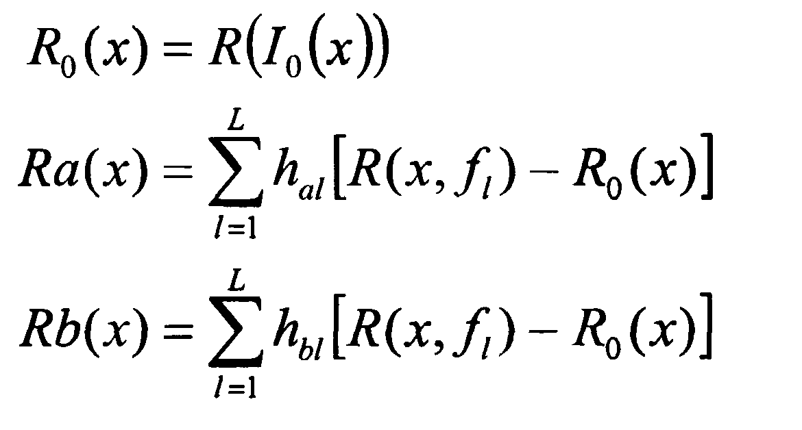
(Eq.32) where ha, and hbt are coefficients defined in (Eq.9). The coefficients only depend on {fufi, ·.· Jl) and possibly weights {IV,, W2, ..., WL}, and they are independent of R(x,fi) or I(x,fi).(Eq.32) where ha, and hbt are coefficients defined in (Eq.9). The coefficients only depend on {fufi, ·. · Jl) and possibly weights {IV ,, W2, ..., WL}, and they are independent of R (x, fi) or I (x, fi).
[086] In general, the resist model R{·} can be separated as:[086] In general, the resist model R {·} can be separated as:

(Eq.33) where Rb is a mask loading bias that is independent of the aerial image l{x) or focus, P{} is the linear filter operation and Pnl{} is some non-linear operation.(Eq.33) where Rb is a mask loading bias that is independent of the aerial image l {x) or focus, P {} is the linear filter operation and Pnl {} is some non-linear operation.
[087] Combining (Eq.32) and (Eq.33),Combining (Eq.32) and (Eq.33),

(Eq.34) [088] As discussed previously, since PQ is a linear operation, then(Eq.34) As discussed previously, since PQ is a linear operation, then

(Eq.35) [089] As expected, it is possible to derive the following result with the aid of (Eq.9) and (Eq.10) set forth above,(Eq.35) As expected, it is possible to derive the following result with the aid of (Eq.9) and (Eq.10) set forth above,

(Eq.36)(Eq.36)
Thus, Ra and Rb can computed fromThus, Ra and Rb can be computed from

(Eq.37) [090] The benefits of this approach are that it does not attempt to capture the differential through-PW behavior for all gauge points using a single linear filter. Rather, this approach minimizes the (RMS) difference for each pixel, thereby improving the overall accuracy. In addition, this approach does not require identification of pattern-specific gauge points or all NC resist contour neighboring points. One drawback is that this approach slightly increases the computation complexity for Ra and Rb. However, since the synthesis of through-PW resist images only require scaling and additions of R0, Ra and Rb, the increase in the computation complexity of the derivative images is generally insignificant compared to the reduction in computation complexity of through-PW resist images, especially for dense PW sampling. iii) Polynomial Approximation of Non-Linear operations [091] In a third approach, non-linear resist model operations are approximated using polynomials. More specifically, for truncation operations on image I(x), for the purpose of emulating acid and base reaction effects, quadratic polynomials of the image provide a sufficient approximation. Another typical non-linear operation, the linear filtering of the image slope, can be expressed precisely as the linear filtering of a quadratic function of the image gradient G{I(x)}=I{x)-I{x-1), thus the quadratic polynomial of the aerial image ƒ(*) itself. More specifically, letting G{} be the gradient operation and the linear filter be Psiope{·}, then this non-linear operation can be expressed as:(Eq.37) The benefits of this approach are that it does not attempt to capture the differential through-PW behavior for all gauge points using a single linear filter. Rather, this approach minimizes the (RMS) difference for each pixel, continuously improving the overall accuracy. In addition, this approach does not require identification or pattern-specific gauge points or all NC resist contour neighboring points. One drawback is that this approach slightly increases the computation complexity for Ra and Rb. However, since the synthesis of through-PW resist images only require scaling and additions of R0, Ra and Rb, the increase in computation complexity or derivative images is generally insignificant compared to the reduction in computation complexity or through-PW resist images, especially for dense PW sampling. iii) Polynomial Approximation of Non-Linear Operations In a third approach, non-linear resist model operations are approximated using polynomials. More specifically, for truncation operations on image I (x), for the purpose of emulating acid and base reaction effects, quadratic polynomials or the image provide a sufficient approximation. Another typical non-linear operation, the linear filtering of the image slope, can be expressed exactly as the linear filtering or a quadratic function of the image gradient G {I (x)} = I {x) -I {x-1) , thus the quadratic polynomial of the aerial image ƒ (*) itself. More specifically, letting G {} be the gradient operation and the linear filter be Psiope {·}, then this non-linear operation can be expressed as:

(Eq.38) [092] To summarize, the resist image from aerial image I(x) can be approximated as:(Eq.38) To summarize, the resist image from aerial image I (x) can be approximated as:

(Eq.39) [093] Once again, P|{·} represents the linear filter for the aerial image term, P2{·} represents the linear filter for the aerial image square term, and Psi0Pe{·} represents the linear filter for the aerial image gradient term, while Rb is a mask loading bias that is independent of the image pattern. Thus the resist image is expressed as a 4th-order polynomial of the defocus value. However, in a typical application, R3M and Ra(x) are very small and cay be ignored to improve the computational efficiency.(Eq.39) [093] Once again, P | {·} represents the linear filter for the aerial image term, P2 {·} represents the linear filter for the aerial image square term, and Psi0Pe {·} represents the linear filter for the aerial image gradient term, while Rb is a mask loading bias that is independent of the image pattern. Thus the resist image is expressed as a 4th-order polynomial of the defocus value. However, in a typical application, R3M and Ra (x) are very small and can be ignored to improve computational efficiency.
[094] As noted above, the goal of lithography design verification is to ensure that printed resist edges and line widths are within a pre-specified distance from the design target. Similarly, the size of the process window -exposure latitude and depth of focus- are defined by CDs or edge placements falling within the specified margin. The various methods outlined above provide very efficient ways to determine the change of resist image signal level with variation of focus and exposure dose or other, generalized PW parameters. Each method resulted in an approximate expression of through-PW resist image variations AR as perturbation of the NC (Nominal Condition) image R0.[094] As mentioned above, the goal of lithography design verification is to ensure that printed resist edges and line widths are within a pre-specified distance from the design target. Similarly, the size of the process window - exposure latitude and depth of focus - are defined by CDs or edge placements falling within the specified margin. The various methods outlined above provide very efficient ways to determine the change of resist image signal level with variation or focus and exposure dose or other, generalized PW parameters. Each method yields an approximate expression or through-PW resist image variations AR as perturbation of the NC (Nominal Condition) image R0.
[095] In order to relate these changes in Λ(χ) to changes in edge placement, in most cases a first-order approximation will suffice, due to the small CD or edge placement tolerances. Therefore, the lateral shift of any resist contour (R=0) (i.e., the edge placement change) is simply approximated by the image gradient G at the original (i.e. NC) contour location and the change in resist image level AR due to variation of focus, dose, etc. as: (Eq.40)[095] In order to relate these changes in Λ (χ) to changes in edge placement, in most cases a first-order approximation will suffice, due to the small CD or edge placement tolerances. Therefore, the lateral shift or any resist contour (R = 0) (ie the edge placement change) is simply approximated by the image gradient G at the original (ie NC) contour location and the change in resist image level AR due to variation or focus, dose, etc. axis: (Eq.40)

where both the initial contour location and the gradient are determined from the resist image at NC, i.e. /?o(*,.y)· The 2-dimensional edge shift can be calculated separately in x and y direction by the partial image derivative in each direction, or as an absolute shift using an absolute gradient value, i.e. the geometrical sum of S*=/?o(*,.y)-/^-1.-^) and ^=^0(^,7)-^0(^7-1), i e., the absolute gradient valuewhere both the initial contour location and gradient are determined from the resist image at NC, ie /?o(*,.y)· The 2-dimensional edge shift can be calculated separately in x and y direction by the partial image derivative in each direction, or as an absolute shift using an absolute gradient value, ie the geometric sum or S * = /? o (* ,. y) - / ^ - 1 .- ^) and ^ = ^ 0 (^, 7) - ^ 0 (^ 7-1), ie the absolute gradient value

[096] From the foregoing explanation, the edge shift can be directly expressed as a function of the differential images defined above:[096] From the foregoing explanation, the edge shift can be directly expressed as a function of the differential images defined above:

(Eq.41) while changes in CD or line widths can be determined from adding the individual edge placement shifts on either side of a line, resulting generally in ACD=2*AEP. Clearly, (Eq.41) will be able to reproduce the typical 2nd order-like through-focus behavior of CD or EPE curves. More importantly, after the set of images such as [R0, P{k}, P{a}, P{b}] has been calculated, which may be accomplished with only ~1x more computation than simulating the single image at NC (assuming that fewer TCC terms are required for sufficient accuracy on the differentials), (Eq.41) may be applied to map out analytically the complete PW for every single edge position on a design, without the need for any further time-consuming image simulation. A generic flow diagram to illustrate this method is provided in Fig. 5.(Eq.41) while changes in CD or line widths can be determined from adding the individual edge placement shifts on either side or a line, resulting generally in ACD = 2 * AEP. Clearly, (Eq.41) will be able to reproduce the typical 2nd order-like through-focus behavior or CD or EPE curves. More importantly, after the set of images such as [R0, P {k}, P {a}, P {b}] has been calculated, which may have been accomplished with only ~ 1x more computation than simulating the single image at NC ( assuming that fewer TCC terms are required for sufficient accuracy on the differentials, (Eq.41) may be applied to map out analytically the complete PW for every single edge position on a design, without the need for any further time-consuming image simulation . A generic flow diagram to illustrate this method is provided in Figs. 5.
[097] Referring to Fig. 5, the first step (Step 80) entails defining the process specific parameters associated with the lithography process and system that will be utilized in the imaging process. Thereafter, derivative TCCs A and B are generated utilizing (Eq.14) (Step 82). In Step 84, calibration test data is acquired for multiple process window conditions. In Step 85, model parameters for RoO and/or associated filter P{} are determined utilizing in part the results of Step 82. Next, the target mask pattern or design is defined (Step 86). The process then proceeds to generate images such as R0(x), P{Io}, P{a) and P{b) in Step 88. Next, the simulated image is synthesized, NC contours are extracted, and feature EPEs are determined at a given set of edge positions {x,} (Step 90). The process then proceeds to Step 92 to determine EPE or CD variations through process window at edge positions {*,}. Finally, in Step 94, the results obtained in Step 92 are analyzed to determine whether the resulting image is within a predefined error tolerance, thus, determining a common process window as well as identifying any problem area (i.e., hot-spots) within the design.Referring to FIG. 5, the first step (Step 80) entails defining the process specific parameters associated with the lithography process and system that will be utilized in the imaging process. Thereafter, derivative TCCs A and B are generated utilizing (Eq.14) (Step 82). In Step 84, calibration test data is acquired for multiple process window conditions. In Step 85, model parameters for RoO and / or associated filter P {} are determined utilizing in part the results of Step 82. Next, the target mask pattern or design is defined (Step 86). The process then proceeds to generate images such as R0 (x), P {Io}, P {a) and P {b) in Step 88. Next, the simulated image is synthesized, NC contours are extracted, and feature EPEs are determined at a given set of edge positions {x,} (Step 90). The process then proceeds to Step 92 to determine EPE or CD variations through process window at edge positions {*,}. Finally, in Step 94, the results obtained in Step 92 are analyzed to determine whether the resulting image is within a predefined error tolerance, thus, determining a common process window as well as identifying any problem area (ie, hot-spots) within the design.
[098] The methods detailed above, and in particular (Eq.41) can be applied very flexibly for a wide range of tasks in lithography design inspection. Some of these applications are briefly outlined below. However, it is noted that the present invention is not limited to the applications disclosed herein.[098] The methods detailed above, and in particular (Eq.41) can be applied very flexibly for a wide range of tasks in lithography design inspection. Some of these applications are briefly outlined below. However, it is noted that the present invention is not limited to the applications disclosed.
[099] For any particular edge or CD, (Eq.41) allows straightforward determination of the focus latitude (=DOF (Depth of Focus)) at nominal dose, for a given tolerance of CD, EP or line end variation.[099] For any particular edge or CD, (Eq.41) allows straightforward determination of the focus latitude (= DOF (Depth of Focus)) at nominal dose, for a given tolerance or CD, EP or line end variation.
[100] For any particular edge or CD, (Eq.41) allows straightforward determination of the exposure dose at nominal focus, for a given tolerance of CD, EP or line end variation.[100] For any particular edge or CD, (Eq.41) allows straightforward determination of the exposure dose at nominal focus, for a given tolerance or CD, EP or line end variation.
[101] For any particular edge or CD, (Eq.41) allows straightforward mapping of the shape, center and area of the PW in {F,E} space or a generalized PW space, for a given tolerance of CD, EP or line end variation.[101] For any particular edge or CD, (Eq.41) allows straightforward mapping of the shape, center and area of the PW in {F, E} space or a generalized PW space, for a given tolerance or CD, EP or line end variation.
[102] For a set of edges or CDs covering the full chip design and all relevant pattern/feature types, the common process window of the design can be efficiently calculated, and process corrections may be derived in order to center the common PW.[102] For a set of edges or CDs covering the full chip design and all relevant pattern / feature types, the common process window or the design can be efficiently calculated, and process corrections may be derived in order to center the common PW.
[103] Critical, limiting patterns may be identified that define the inner boundaries of the common PW, by either having off-centered PWs or small PWs.[103] Critical, limiting patterns may be identified as defining the inner boundaries of the common PWs, by either having off-centered PWs or small PWs.
[104] The common PW area may be mapped out as a function of tolerance specs on EP or CD variations. This sensitivity analysis may provide a yield estimate depending on design sensitivity.[104] The common PW area may be mapped out as a function of tolerance specs on EP or CD variations. This sensitivity analysis may provide a yield estimate depending on design sensitivity.
[105] Design hot spots may be identified from a full-chip analysis using (Eq.41), as patterns with PW area, DOF or exposure latitude falling below a certain threshold. The behavior of these critical patterns may then be investigated in detail by full-PW simulations, i.e. using the full simulation model for repeated image and resist contour simulation at many points across the PW.[105] Design hot spots may be identified from a full-chip analysis using (Eq.41), as patterns with PW area, DOF or exposure latitude falling below a certain threshold. The behavior of these critical patterns may then be investigated in detail by full PW simulations, i.e. using the full simulation model for repeated image and resist contour simulation at many points across the PW.
[106] Fig. 6 is a block diagram that illustrates a computer system 100 which can assist in the simulation method disclosed herein. Computer system 100 includes a bus 102 or other communication mechanism for communicating information, and a processor 104 coupled with bus 102 for processing information. Computer system 100 also includes a main memory 106, such as a random access memory (RAM) or other dynamic storage device, coupled to bus 102 for storing information and instructions to be executed by processor 104. Main memory 106 also may be used for storing temporary variables or other intermediate information during execution of instructions to be executed by processor 104. Computer system 100 further includes a read only memory (ROM) 108 or other static storage device coupled to bus 102 for storing static information and instructions for processor 104. A storage device 110, such as a magnetic disk or optical disk, is provided and coupled to bus 102 for storing information and instructions.FIG. 6 is a block diagram that illustrates a computer system 100 which can assist in the simulation method disclosed. Computer system 100 includes a bus 102 or other communication mechanism for communicating information, and a processor 104 coupled with bus 102 for processing information. Computer system 100 also includes a main memory 106, such as a random access memory (RAM) or other dynamic storage device, coupled to bus 102 for failure information and instructions for executed by processor 104. Main memory 106 also may be used for failure temporary variables or other intermediate information during execution of instructions to be executed by processor 104. Computer system 100 further includes a read-only memory (ROM) 108 or other static storage device coupled to bus 102 for failure static information and instructions for processor 104. A storage device 110, such as a magnetic disk or optical disk, is provided and coupled to bus 102 for malfunction information and instructions.
Computer system 100 may be coupled via bus 102 to a display 112, such as a cathode ray tube (CRT) or flat panel or touch panel display for displaying information to a computer user. An input device 114, including alphanumeric and other keys, is coupled to bus 102 for communicating information and command selections to processor 104. Another type of user input device is cursor control 116, such as a mouse, a trackball, or cursor direction keys for communicating direction information and command selections to processor 104 and for controlling cursor movement on display 112. This input device typically has two degrees of freedom in two axes, a first axis (e.g., x) and a second axis (e.g., y), that allows the device to specify positions in a plane. A touch panel (screen) display may also be used as an input device.Computer system 100 may be coupled via bus 102 to a display 112, such as a cathode ray tube (CRT) or flat panel or touch panel display for displaying information to a computer user. An input device 114, including alphanumeric and other keys, is coupled to bus 102 for communicating information and command selections to processor 104. Another type of user input device is cursor control 116, such as a mouse, a trackball, or cursor direction keys for communicating direction information and command selections to processor 104 and for controlling cursor movement on display 112. This input device typically has two degrees of freedom in two axes, a first axis (eg, x) and a second axis (eg, y), that allows the device to specify positions in a plane. A touch panel (screen) display may also be used as an input device.
[107] According to one embodiment of the invention, portions of the simulation process may be performed by computer system 100 in response to processor 104 executing one or more sequences of one or more instructions contained in main memory 106. Such instructions may be read into main memory 106 from another computer-readable medium, such as storage device 110. Execution of the sequences of instructions contained in main memory 106 causes processor 104 to perform the process steps described herein. One or more processors in a multi-processing arrangement may also be employed to execute the sequences of instructions contained in main memory 106. In alternative embodiments, hard-wired circuitry may be used in place of or in combination with software instructions to implement the invention. Thus, embodiments of the invention are not limited to any specific combination of hardware circuitry and software. The term "computer-readable medium" as used herein refers to any medium that participates in providing instructions to processor 104 for execution. Such a medium may take many forms, including but not limited to, non-volatile media, volatile media, and transmission media. Non-volatile media include, for example, optical or magnetic disks, such as storage device 110. Volatile media include dynamic memory, such as main memory 106. Transmission media include coaxial cables, copper wire and fiber optics, including the wires that comprise bus 102. Transmission media can also take the form of acoustic or light waves, such as those generated during radio frequency (RF) and infrared (IR) data communications. Common forms of computer-readable media include, for example, a floppy disk, a flexible disk, hard disk, magnetic tape, any other magnetic medium, a CD-ROM, DVD, any other optical medium, punch cards, paper tape, any other physical medium with patterns of holes, a RAM, a PROM, and EPROM, a FLASH-EPROM, any other memory chip or cartridge, a carrier wave as described hereinafter, or any other medium from which a computer can read.[107] According to one embodiment of the invention, portions of the simulation process may be performed by computer system 100 in response to processor 104 executing one or more sequences or one or more instructions contained in main memory 106. Such instructions may be read into main memory 106 from another computer-readable medium, such as storage device 110. Execution of the sequences of instructions contained in main memory 106 causes processor 104 to perform the process steps described. One or more processors in a multi-processing arrangement may also be used to execute the sequences of instructions contained in main memory 106. In alternative expired, hard-wired circuitry may be used in place or in combination with software instructions to implement the invention . Thus, the invention or the invention are not limited to any specific combination of hardware circuitry and software. The term "computer-readable medium" as used refers to any medium that participates in providing instructions to processor 104 for execution. Such a medium may take many forms, including but not limited to, non-volatile media, volatile media, and transmission media. Non-volatile media include, for example, optical or magnetic disks, such as storage device 110. Volatile media include dynamic memory, such as main memory 106. Transmission media include coaxial cables, copper wire and fiber optics, including the wires that include bus 102. Transmission media can also take the form of acoustic or light waves, such as those generated during radio frequency (RF) and infrared (IR) data communications. Common forms of computer-readable media include, for example, a floppy disk, a flexible disk, hard disk, magnetic tape, any other magnetic medium, a CD-ROM, DVD, any other optical medium, punch cards, paper tape, any other physical medium with patterns of holes, a RAM, a PROM, and EPROM, a FLASH-EPROM, any other memory chip or cartridge, a carrier wave as described hereinafter, or any other medium from which a computer can read.
[108] Various forms of computer readable media may be involved in carrying one or more sequences of one or more instructions to processor 104 for execution. For example, the instructions may initially be borne on a magnetic disk of a remote computer. The remote computer can load the instructions into its dynamic memory and send the instructions over a telephone line using a modem. A modem local to computer system 100 can receive the data on the telephone line and use an infrared transmitter to convert the data to an infrared signal. An infrared detector coupled to bus 102 can receive the data carried in the infrared signal and place the data on bus 102. Bus 102 carries the data to main memory 106, from which processor 104 retrieves and executes the instructions. The instructions received by main memory 106 may optionally be stored on storage device 110 either before or after execution by processor 104.[108] Various forms of computer readable media may be involved in carrying one or more sequences or one or more instructions to processor 104 for execution. For example, the instructions may be borne on a magnetic disk or a remote computer. The remote computer can load the instructions into its dynamic memory and send the instructions about a telephone line using a modem. A modem local to computer system 100 can receive the data on the telephone line and use an infrared transmitter to convert the data to an infrared signal. An infrared detector coupled to bus 102 can receive the data carried in the infrared signal and place the data on bus 102. Bus 102 carries the data to main memory 106, from which processor 104 retrieves and executes the instructions. The instructions received by main memory 106 may optionally be stored on storage device 110 either before or after execution by processor 104.
[109] Computer system 100 also preferably includes a communication interface 118 coupled to bus 102. Communication interface 118 provides a two-way data communication coupling to a network link 120 that is connected to a local network 122. For example, communication interface 118 ma> toe an integrated services digital network (ISDN) card or a modem to provide a data comm unication connection to a corresponding type of telephone line. As another example, communication interface 118 may be a local area network (LAN) card to provide a data communication connection to a compatible LAN. Wireless links may also be implemented. In any such implementation, communication interface 118 sends and receives electrical, electromagnetic or optical signals that carry digital data streams representing various types of information.[109] Computer system 100 also preferably includes a communication interface 118 coupled to bus 102. Communication interface 118 provides a two-way data communication link to a network link 120 that is connected to a local network 122. For example, communication interface 118 ma > to an integrated services digital network (ISDN) card or a modem to provide a data communication connection to a corresponding type of telephone line. As another example, communication interface 118 may be a local area network (LAN) card to provide a data communication connection to a compatible LAN. Wireless links may also be implemented. In any such implementation, communication interface 118 sends and receives electrical, electromagnetic or optical signals that carry digital data streams representing various types of information.
Network link 120 typically provides data communication through one or more networks to other data devices. For example, network link 120 may provide a connection through local network 122 to a host computer 124 or to d ata equipment operated by an Internet Service Provider (ISP) 126. ISP 126 in turn provides data communication services through the worldwide packet data communication network, now commonly referred to as the "Internet" 128. Local network 122 and Internet 128 both use electrical, electromagnetic or optical signals that carry digital data streams. The signals through the various networks and the signals on network link 120 and through communication interface 118, which carry the digital data to and from computer system 100, are exemplary forms of carrier waves transporting the information.Network link 120 typically provides data communication through one or more networks to other data devices. For example, network link 120 may provide a connection through local network 122 to a host computer 124 or to d ata equipment operated by an Internet Service Provider (ISP) 126. ISP 126 in turn provides data communication services through the worldwide packet data communication network , now commonly referred to as the "Internet" 128. Local network 122 and Internet 128 both use electrical, electromagnetic or optical signals that carry digital data streams. The signals through the various networks and the signals on network link 120 and through communication interface 118, which carry the digital data to and from computer system 100, are exemplary forms of carrier waves transporting the information.
[110] Computer system 100 can send messages and receive data, including program code, through the network(s), network link 120, and communication interface 118. In the Internet example, a server 130 might transmit a requested code for an application program through Internet 128, ISP 126, local network 122 and communication interface 118. In accordance with the invention, one such downloaded application provides for the illumination optimization of the embodiment, for example. The received code may be executed by processor 104 as it is received, and/or stored in storage device 110, or other non-volatile storage for later execution. In this manner, computer system 100 may obtain application code in the form of a carrier wave.[110] Computer system 100 can send messages and receive data, including program code, through the network (s), network link 120, and communication interface 118. In the Internet example, a server 130 might transmit a requested code for an application program through Internet 128, ISP 126, local network 122 and communication interface 118. In accordance with the invention, one such downloaded application provides for the illumination optimization of the embodiment, for example. The received code may be executed by processor 104 if it is received, and / or stored in storage device 110, or other non-volatile storage for later execution. In this manner, computer system 100 may obtain application code in the form of a carrier wave.
[111] Fig. 7 schematically depicts an exemplary lithographic projection apparatus whose performance could be simulated utilizing the process of present invention. The apparatus comprises: - a radiation system Ex, IL, for supplying a projection beam PB of radiation. In this particular case, the radiation system also comprises a radiation source LA; - a first object table (mask table) MT provided with a mask holder for holding a mask MA (e.g., a reticle), and connected to first positioning means for accurately positioning the mask with respect to item PL; - a second object table (substrate table) WT provided with a substrate holder for holding a substrate W (e.g., a resist-coated silicon wafer), and connected to second positioning means for accurately positioning the substrate with respect to item PL; - a projection system ("lens") PL (e.g., a refractive, catoptric or catadioptric optical system) for imaging an irradiated portion of the mask MA onto a target portion C (e.g., comprising one or more dies) of the substrate W.FIG. 7 schematically depicts an exemplary lithographic projection apparatus whose performance could be simulated utilizing the process of present invention. The apparatus comprises: - a radiation system Ex, IL, for supplying a projection beam PB or radiation. In this particular case, the radiation system also comprises a radiation source LA; - a first object table (mask table) MT provided with a mask holder for holding a mask MA (e.g., a reticle), and connected to first positioning means for accurately positioning the mask with respect to item PL; - a second object table (substrate table) WT provided with a substrate holder for holding a substrate W (e.g., a resist-coated silicon wafer), and connected to second positioning means for accurately positioning the substrate with respect to item PL; a projection system ("lens") PL (e.g., refractive, catoptric or catadioptric optical system) for imaging an irradiated portion of the mask MA onto a target portion C (e.g., including one or more dies) or the substrate W.
[112] As depicted herein, the apparatus is of a transmissive type (Le., has a transmissive mask). However, in general, it may also be of a reflect!we type, for example (with a reflective mask). Alternatively, the apparatus may employ another kind of patterning means as an alternative to the use of a mask; examples include a programmable mirror array or LCD matrix.[112] As depicted, the apparatus is of a transmissive type (Le., Has a transmissive mask). However, in general, it may also be a reflect! We type, for example (with a reflective mask). Alternatively, the apparatus may employ another child or patterning means as an alternative to the use of a mask; examples include a programmable mirror array or LCD matrix.
[113] The source LA (e.g., a mercury lamp or excimer laser) produces a beam of radiation. This beam is fed into an illumination system (illuminator) IL, either directly or after having traversed conditioning means, such as a beam expander Ex, for example. The illuminator IL may comprise adjusting means AM for setting the outer and/or inner radial extent (commonly referred to as σ-outer and σ-inner, respectively) of the intensity distribution in the beam. In addition, it will generally comprise various other components, such as an integrator IN and a condenser CO. In this way, the beam PB impinging on the mask MA has a desired uniformity and intensity distribution in its cross-section.[113] The source LA (e.g., a mercury lamp or excimer laser) produces a beam of radiation. This beam is fed into an illumination system (illuminator) IL, either directly or after having traversed conditioning means, such as a beam expander Ex, for example. The illuminator IL may include adjusting means AM for setting the outer and / or inner radial extent, or the intensity distribution in the beam. In addition, it will generally include various other components, such as an integrator, and a condenser CO. In this way, the beam PB impinging on the mask MA has a desired uniformity and intensity distribution in its cross-section.
[114] It should be noted with regard to Fig. 7 that the source LA may be within the housing of the lithographic projection apparatus (as is often the case when the source LA is a mercury lamp, for example), but that it may also be remote from the lithographic projection apparatus, the radiation beam that it produces being led into the apparatus (e.g., with the aid of suitable directing mirrors); this latter scenario is often the case when the source LA is an excimer laser (e.g., based on KrF, ArF or F2 lasing). The current invention encompasses at least both of these scenarios.[114] It should be noted with regard to Figs. 7 that the source LA may be within the housing of the lithographic projection apparatus (as is often the case when the source LA is a mercury lamp, for example), but that may also be remote from the lithographic projection apparatus, the radiation beam that it produces being led into the apparatus (eg, with the aid of suitable directing mirrors); this latter scenario is often the case when the source LA is an excimer laser (e.g., based on KrF, ArF or F2 lasing). The current invention and compasses at least both of these scenarios.
[115] The beam PB subsequently intercepts the mask MA, which is held on a mask table MT. Having traversed the mask MA, the beam PB passes through the lens PL, which focuses the beam PB onto a target portion C of the substrate W. With the aid of the second positioning means (and interferometric measuring means IF), the substrate table WT can be moved accurately, e.g. so as to position different target portions C in the path of the beam PB. Similarly, the first positioning means can be used to accurately position the mask MA with respect to the path of the beam PB, e.g., after mechanical retrieval of the mask MA from a mask library, or during a scan. In general, movement of the object tables MT, WT will be realized with the aid of a long-stroke module (coarse positioning) and a short-stroke module (fine positioning), which are not explicitly depicted in Fig. 7. However, in the case of a wafer stepper (as opposed to a step-and-scan tool) the mask table MT may just be connected to a short stroke actuator, or may be fixed.[115] The beam PBiter intercepts the mask MA, which is a hero on a mask table MT. Having traversed the mask MA, the beam PB passes through the lens PL, which marked the beam PB onto a target portion C of the substrate W. With the aid of the second positioning means (and interferometric measuring means IF), the substrate table WT can be moved accurately, eg so as to position different target portions C in the path of the beam PB. Similarly, the first positioning means can be used to accurately position the mask MA with respect to the path of the beam PB, e.g., after mechanical retrieval of the mask MA from a mask library, or during a scan. In general, movement of the object tables MT, WT will be realized with the aid of a long-stroke module (coarse positioning) and a short-stroke module (fine positioning), which are not explicitly depicted in FIG. 7. However, in the case of a wafer stepper (as opposed to a step-and-scan tool) the mask table MT may just be connected to a short-stroke actuator, or may be fixed.
[116] The depicted tool can be used in two different modes: - In step mode, the mask table MT is kept essentially stationary, and an entire mask image is projected in one go (/.e., a single "flash") onto a target portion C. The substrate table WT is then shifted in the x and/or y directions so that a different target portion C can be irradiated by the beam PB; - In scan mode, essentially the same scenario applies, except that a given target portion C is not exposed in a single "flash". Instead, the mask table MT is movable in a given direction (the so-called "scan direction", e.g., the y direction) with a speed v, so that the projection beam PB is caused to scan over a mask image; concurrently, the substrate table WT is simultaneously moved in the same or opposite direction at a speed V = Mv, in which M is the magnification of the lens PL (typically, M = 1/4 or 1/5). In this manner, a relatively large target portion C can be exposed, without having to compromise on resolution.[116] The depicted tool can be used in two different modes: - In step mode, the mask table MT is kept essentially stationary, and an entire mask image is projected in one go (/.e., A single "flash") onto a target portion C. The substrate table WT is then shifted in the x and / or y directions so that a different target portion C can be irradiated by the beam PB; - In scan mode, essentially the same scenario applies, except that a given target portion C is not exposed in a single "flash". Instead, the mask table MT is movable in a given direction (the so-called "scan direction", e.g., the y direction) with a speed v, so that the projection beam PB is caused to scan over a mask image; concurrently, the substrate table WT is simultaneously moved in the same or opposite direction at a speed V = Mv, in which M is the magnification of the lens PL (typically, M = 1/4 or 1/5). In this manner, a relatively large target portion C can be exposed, without having to compromise on resolution.
[117] The concepts disclosed herein may simulate or mathematically model any generic imaging system for imaging sub wavelength features, and may be especially useful with emerging imaging technologies capable of producing wavelengths of an increasingly smaller size. Emerging technologies already in use include EUV (extreme ultra violet) lithography that is capable of producing a 193nm wavelength with the use of a ArF laser, and even a 157nm wavelength with the use of a Fluorine laser. Moreover, EUV lithography is capable of producing wavelengths within a range of 20-5nm by using a synchrotron or by hitting a material (either solid or a plasma) with high energy electrons in order to produce photons within this range. Because most materials are absorptive within this range, illumination may be produced by reflective mirrors with a multi-stack of Molybdenum and Silicon. The multi-stack mirror has a 40 layer pairs of Molybdenum and Silicon where the thickness of each layer is a quarter wavelength. Even smaller wavelengths may be produced with X-ray lithography. Typically, a synchrotron is used to produce an X-ray wavelength. Since most material is absorptive at x-ray wavelengths, a thin piece of absorbing material defines where features would print (positive resist) or not print (negative resist).[117] The concepts disclosed may simulate or mathematically model any generic imaging system for imaging sub wavelength features, and may be especially useful with emerging imaging technologies capable of producing wavelengths or an increasingly smaller size. Emerging technologies already in use include EUV (extreme ultra violet) lithography that is capable of producing a 193nm wavelength with the use of an ArF laser, and even a 157nm wavelength with the use of a Fluorine laser. Moreover, EUV lithography is capable of producing wavelengths within a range of 20-5nm by using a synchrotron or by hitting a material (either solid or a plasma) with high energy electrons in order to produce photons within this range. Because most materials are absorptive within this range, illumination may be produced by reflective mirrors with a multi-stack of Molybdenum and Silicon. The multi-stack mirror has 40 layer pairs of Molybdenum and Silicon where the thickness of each layer is a quarter wavelength. Even narrower wavelengths may be produced with X-ray lithography. Typically, a synchrotron is used to produce an X-ray wavelength. Since most material is absorptive at x-ray wavelengths, a thin piece of absorbing material defines where features would print (positive resist) or not print (negative resist).
[118] While the concepts disclosed herein may be used for imaging on a substrate such as a silicon wafer, it shall be understood that the disclosed concepts may be used with any type of lithographic imaging systems, e.g., those used for imaging on substrates other than silicon wafers.[118] While the concepts disclosed may be used for imaging on a substrate such as a silicon wafer, it shall be understood that the disclosed concepts may be used for any type of lithographic imaging systems, eg, those used for imaging on substrates other than silicon wafers.
[119] Although the present invention has been described and illustrated in detail, it is to be clearly understood that the same is by way of illustration and example only and is not to be taken by way of limitation, the scope of the present invention being limited only by the terms of the appended clauses. Other aspects of the invention are set out as in the following numbered clauses: 1. A method of simulating imaging performance of a lithographic process utilized to image a target design having a plurality of features, said method comprising: determining a function for generating a simulated image, said function accounting for process window variations associated with said lithographic process; and generating said simulated image utilizing said function; said simulated image representing the imaging result of said target design for said lithographic process. 2. The method of simulating imaging performance of a lithographic process according to clause 1, wherein said function includes a polynomial function of the process window variations, and said process window variations include variations in at least one of focus and exposure dose. 3. The method of simulating imaging performance of a lithographic process according to clause 2, wherein said process window variations further include variations in optical settings including at least one of numerical aperture and sigma. 4. The method of simulating imaging performance of a lithographic process according to clause 2, wherein said function is defined as:[119] Although the present invention has been described and illustrated in detail, it is clearly understood that the same is by way of illustration and example only and is not to be done by way of limitation, the scope of the present invention being limited only by the terms of the appended clauses. Other aspects of the invention are set out as in the following numbered clauses: 1. A method of simulating imaging performance or a lithographic process utilized to image a target design having a variety of features, said method including: determining a function for generating a simulated image, said function accounting for process window variations associated with said lithographic process; and generating said simulated image utilizing said function; said simulated image representing the imaging result or said target design for said lithographic process. 2. The method of simulating imaging performance of a lithographic process according to clause 1, said said function includes a polynomial function or the process window variations, and said process window variations include variations in at least one of focus and exposure dose. 3. The method of simulating imaging performance of a lithographic process according to clause 2, said process window variations further include variations in optical settings including at least one of numerical aperture and sigma. 4. The method of simulating imaging performance or a lithographic process according to clause 2, said said function is defined as:

where to represents image intensity at nominal focus and exposure, fo represents nominal focus, ƒ and ε represents an actual focus-exposure level at which the simulated image is calculated, and parameter V and "£>" represent first order and second order derivative images with respect to focus change. 5. The method of simulating imaging performance of a lithographic process according to clause 2, wherein said function is defined as:where to represents image intensity at nominal focus and exposure, fo represents nominal focus, and represents an actual focus-exposure level at which the simulated image is calculated, and parameter V and "£>" represent first order and second order derivative images with respect to focus change. 5. The method of simulating imaging performance or a lithographic process according to clause 2, said said function is defined as:

where lo represents image intensity at nominal focus and exposure, fo represents nominal focus, ƒ and ε represents an actual focus-exposure level at which the simulated image is calculated, and parameter "a" and "b" represent best fit of a series of aerial images at different focuses. 6. The method of simulating imaging performance of a lithographic process according to clause 2, wherein said function is defined as:where lo represents image intensity at nominal focus and exposure, fo represents nominal focus, and represents an actual focus-exposure level at which the simulated image is calculated, and parameter "a" and "b" represent best fit of a series of aerial images at different. 6. The method of simulating imaging performance or a lithographic process according to clause 2, said said function is defined as:

where l0 represents image intensity at nominal focus and exposure, fo represents nominal focus, ƒ and ε represents an actual focus-exposure level at which the simulated image is calculated, and parameter V and "b" represent the aerial images computed from TCCs A and B which are linear combinations of a series of TCCs at different focuses. 7. The method of simulating imaging performance of a lithographic process according to clause 2, wherein said function is defined as:where l0 represents image intensity at nominal focus and exposure, fo represents nominal focus, and represents an actual focus-exposure level at which the simulated image is calculated, and parameter V and "b" represent the aerial images computed from TCCs A and B which are linear combinations or a series or TCCs at different differ. 7. The method of simulating imaging performance or a lithographic process according to clause 2, said function is defined as:

where fo represents image intensity at nominal focus and exposure, fo represents nominal focus, ƒ and ε represents an actual focus-exposure level at which the simulated image is calculated, and parameter V and "b" represent the aerial images computed from TCCs A and B which are first order and second order derivative TCCs with respect to focus change. 8. The method of simulating imaging performance of a lithographic process according to clause 1, wherein said simulated image corresponds to a resist image. 9. The method of simulating imaging performance of a lithographic process according to clause 8, wherein said function for simulating said resist image with focus and dose variation is defined as:where fo represents image intensity at nominal focus and exposure, fo represents nominal focus, and represents an actual focus-exposure level at which the simulated image is calculated, and parameter V and "b" represent the aerial images computed from TCCs A and B which are first order and second order derivative TCCs with respect to focus change. 8. The method of simulating imaging performance or a lithographic process according to clause 1, said simulated image according to a resist image. 9. The method of simulating imaging performance or a lithographic process according to clause 8, said said function for simulating said resist image with focus and dose variation is defined as:

where Ro represents image intensity at nominal focus and exposure, fo represents nominal aerial image, ƒ and ε represents an actual focus-exposure level at which the simulated image is calculated, parameter V and "b" represent first order and second order derivative aerial images with respect to focus change, P{} denotes the functional action of applying a filter as a resist model. 10. The method of estimating feature edge shift or critical dimension (CD) change due to process window parameter variation of a lithographic process, said method comprising the steps of: determining a function for generating a simulated image, said function accounting for process window variations associated with said lithographic process; generating said simulated image utilizing said function; said simulated image representing the imaging result of said target design for said lithographic process; and estimating said feature edge shift or CD change by analyzing said simulated image. 11. The method of estimating feature edge shift or CD change due to process window parameter variation of a lithographic process according to clause 10, wherein said function accounts for variations in focus and dose variation, said function being defined as:where Ro represents image intensity at nominal focus and exposure, represents nominal aerial image, and represents an actual focus-exposure level at which the simulated image is calculated, parameter V and "b" represent first order and second order derivative aerial images with respect to focus change, P {} denotes the functional action or applying a filter as a resist model. 10. The method of estimating feature edge shift or critical dimension (CD) change due to process window parameter variation of a lithographic process, said method including the steps of: determining a function for generating a simulated image, said function accounting for process window variations associated with said lithographic process; generating said simulated image utilizing said function; said simulated image representing the imaging result or said target design for said lithographic process; said estimating feature edge shift or CD change by analyzing said simulated image. 11. The method of estimating feature edge shift or CD change due to process window parameter variation of a lithographic process according to clause 10, said function accounts for variations in focus and dose variation, said function being defined as:

where S represents resist image slope at nominal focus and exposure, fa represents nominal aerial image, ƒ and ε represents an actual focus-exposure level at which the simulated image is calculated, parameter V and "b" represent first order and second order derivative aerial images with respect to focus change, P{} denotes a functional action of applying a filter as the resist model. 12. A computer program product having a computer readable medium bearing a computer program for simulating imaging performance of a lithographic process utilized to image a target design having a plurality of features, the computer program, when executed, causing a computer to perform the steps of: determining a function for generating a simulated image, said function accounting for process variations associated with said lithographic process; and generating said simulated image utilizing said function; said simulated image representing the imaging result of said target design for said lithographic process. 13. The computer program product of clause 12, wherein said function includes a polynomial function of the process window variations, and said process window variations include variations in at least one of focus and exposure dose. 14. The computer program product of clause 13, wherein said process window variations further include variations in optical settings including at least one of numerical aperture and sigma. 15. The computer program product according to clause 12, wherein said function for simulating aerial images with focus and dose (exposure) variation is defined as:where S represents resist image slope at nominal focus and exposure, fa represents nominal aerial image, and represents an actual focus-exposure level at which the simulated image is calculated, parameter V and "b" represent first order and second order derivative aerial images with respect to focus change, P {} denotes a functional action or applying a filter as the resist model. 12. A computer program product having a computer readable medium bearing a computer program for simulating imaging performance of a lithographic process utilized to image a target design having a variety of features, the computer program, when executed, causing a computer to perform the steps of : determining a function for generating a simulated image, said function accounting for process variations associated with said lithographic process; and generating said simulated image utilizing said function; said simulated image representing the imaging result or said target design for said lithographic process. 13. The computer program product or clause 12, said said function includes a polynomial function of the process window variations, and said process window variations include variations in at least one of focus and exposure dose. 14. The computer program product or clause 13, said said process window variations further include variations in optical settings including at least one of numerical aperture and sigma. 15. The computer program product according to clause 12, said said function for simulating aerial images with focus and dose (exposure) variation is defined as:

where fa represents image intensity at nominal focus and exposure, fo represents nominal focus, ƒ and ε represents an actual focus-exposure level at which the simulated image is calculated, and parameter V and "b" represent first order and second order derivative images with respect to focus change. 16. The computer program product according to clause 12, wherein said function for simulating aerial images with focus and dose (exposure) variation is defined as:where fa represents image intensity at nominal focus and exposure, fo represents nominal focus, and represents an actual focus-exposure level at which the simulated image is calculated, and parameter V and "b" represent first order and second order derivative images with respect to focus change. 16. The computer program product according to clause 12, said said function for simulating aerial images with focus and dose (exposure) variation is defined as:

where fa represents image intensity at nominal focus and exposure, fo represents nominal focus, ƒ and ε represents an actual focus-exposure level at which the simulated image is calculated, and parameter "a" and "b" represent best fit of a series of aerial images at different focuses. 17. The computer program product according to clause 12, wherein said function for simulating aerial images with focus and dose (exposure) variation is defined as:where fa represents image intensity at nominal focus and exposure, fo represents nominal focus, and represents an actual focus-exposure level at which the simulated image is calculated, and parameter "a" and "b" represent best fit of a series of aerial images at different. 17. The computer program product according to clause 12, said said function for simulating aerial images with focus and dose (exposure) variation is defined as:

where l0 represents image intensity at nominal focus and exposure, fo represents nominal focus, ƒ and ε represents an actual focus-exposure level at which the simulated image is calculated, and parameter V and "b" represent the aerial images computed from TCCs A and B which are linear combinations of a series of TCCs at different focuses. 18. The computer program product according to clause 12, wherein said function for simulating aerial images with focus and dose (exposure) variation is defined as:where l0 represents image intensity at nominal focus and exposure, fo represents nominal focus, and represents an actual focus-exposure level at which the simulated image is calculated, and parameter V and "b" represent the aerial images computed from TCCs A and B which are linear combinations or a series or TCCs at different differ. 18. The computer program product according to clause 12, said said function for simulating aerial images with focus and dose (exposure) variation is defined as:

where fa represents image intensity at nominal focus and exposure, /0represents nominal focus, ƒ and ε represents an actual focus-exposure level at which the simulated image is calculated, and parameter V and "b" represent the aerial images computed from TCCs A and B which are first order and second order derivative TCCs with respect to focus change. 19. The computer program product according to clause 15, wherein said simulated image corresponds to a resist image. 20. The computer program product according to clause 19, wherein said function for simulating said resist image with focus and dose variation is defined as:where fa represents image intensity at nominal focus and exposure, / 0represents nominal focus, and represents an actual focus-exposure level at which the simulated image is calculated, and parameter V and "b" represent the aerial images computed from TCCs A and B which are first order and second order derivative TCCs with respect to focus change. 19. The computer program product according to clause 15, said said simulated image conform to a resist image. 20. The computer program product according to clause 19, said said function for simulating said resist image with focus and dose variation is defined as:

where R0 represents image intensity at nominal focus and exposure, Iq represents nominal aerial image,/and ε represents an actual focus-exposure level at which the simulated image is calculated, parameter V and "b" represent first order and second order derivative aerial images with respect to focus change, P{} denotes the functional action of applying a filter as a resist model. 21. The computer program product having a computer readable medium bearing a computer program for estimating feature edge shift or critical dimension (CD) change due to process window parameter variation of a lithographic process, the computer program, when executed, causing a computer to perform the steps of: determining a function for generating a simulated image, said function accounting for process window variations associated with said lithographic process; generating said simulated image utilizing said function; said simulated image representing the imaging result of said target design for said lithographic process; and estimating said feature edge shift or CD change by analyzing said simulated image. 22. The computer program product according to clause 21, wherein said function accounts for variations in focus and dose variation, said function being defined as:where R0 represents image intensity at nominal focus and exposure, Iq represents nominal aerial image, / and represents a current focus-exposure level at which the simulated image is calculated, parameter V and "b" represent first order and second order derivative aerial images with respect to focus change, P {} denotes the functional action or applying a filter as a resist model. 21. The computer program product having a computer readable medium bearing a computer program for estimating feature edge shift or critical dimension (CD) change due to process window parameter variation of a lithographic process, the computer program, when executed, causing a computer to perform the steps of: determining a function for generating a simulated image, said function accounting for process window variations associated with said lithographic process; generating said simulated image utilizing said function; said simulated image representing the imaging result or said target design for said lithographic process; said estimating feature edge shift or CD change by analyzing said simulated image. 22. The computer program product according to clause 21, said function accounts for variations in focus and dose variation, said function being defined as:

where S represents resist image slope at nominal focus and exposure, Iq represents nominal aerial image, ƒ and ε represents an actual focus-exposure level at which the simulated image is calculated, parameter V and ub" represent first order and second order derivative aerial images with respect to focus change, P{} denotes the functional action of applying a filter as the resist model.where S represents resist image slope at nominal focus and exposure, Iq represents nominal aerial image, and represents a current focus-exposure level at which the simulated image is calculated, parameter V and ub "represent first order and second order derivative aerial images with respect to focus change, P {} denotes the functional action or applying a filter as the resist model.
Claims (1)
Priority Applications (4)
| Application Number | Priority Date | Filing Date | Title |
|---|---|---|---|
| NL2003143A NL2003143A1 (en) | 2008-07-07 | 2009-07-07 | Illumination optimization. |
| US13/003,294 US8542340B2 (en) | 2008-07-07 | 2009-07-07 | Illumination optimization |
| PCT/US2009/049792 WO2010005957A1 (en) | 2008-07-07 | 2009-07-07 | Illumination optimization |
| TW098123009A TW201007383A (en) | 2008-07-07 | 2009-07-07 | Illumination optimization |
Applications Claiming Priority (2)
| Application Number | Priority Date | Filing Date | Title |
|---|---|---|---|
| US99254607P | 2007-12-05 | 2007-12-05 | |
| US99254607 | 2007-12-05 |
Publications (1)
| Publication Number | Publication Date |
|---|---|
| NL1036189A1 true NL1036189A1 (en) | 2009-06-08 |
Family
ID=40734528
Family Applications (1)
| Application Number | Title | Priority Date | Filing Date |
|---|---|---|---|
| NL1036189A NL1036189A1 (en) | 2007-12-05 | 2008-11-12 | Methods and System for Lithography Process Window Simulation. |
Country Status (6)
| Country | Link |
|---|---|
| US (3) | US8200468B2 (en) |
| JP (2) | JP5016585B2 (en) |
| KR (1) | KR101043016B1 (en) |
| CN (1) | CN101452221B (en) |
| NL (1) | NL1036189A1 (en) |
| TW (1) | TWI402631B (en) |
Families Citing this family (229)
| Publication number | Priority date | Publication date | Assignee | Title |
|---|---|---|---|---|
| US20090306941A1 (en) * | 2006-05-15 | 2009-12-10 | Michael Kotelyanskii | Structure Model description and use for scatterometry-based semiconductor manufacturing process metrology |
| US8611637B2 (en) * | 2007-01-11 | 2013-12-17 | Kla-Tencor Corporation | Wafer plane detection of lithographically significant contamination photomask defects |
| NL1036018A1 (en) * | 2007-10-09 | 2009-04-15 | Asml Netherlands Bv | A method of optimizing a model, a method of measuring a property, a device manufacturing method, a spectrometer and a lithographic apparatus. |
| JP5040803B2 (en) * | 2008-05-15 | 2012-10-03 | 富士通セミコンダクター株式会社 | Program and recording medium |
| WO2010005957A1 (en) * | 2008-07-07 | 2010-01-14 | Brion Technologies, Inc. | Illumination optimization |
| US7954071B2 (en) * | 2008-10-31 | 2011-05-31 | Synopsys, Inc. | Assist feature placement based on a focus-sensitive cost-covariance field |
| NL2003699A (en) | 2008-12-18 | 2010-06-21 | Brion Tech Inc | Method and system for lithography process-window-maximixing optical proximity correction. |
| US8402399B2 (en) * | 2010-04-30 | 2013-03-19 | International Business Machines Corporation | Method and system for computing fourier series coefficients for mask layouts using FFT |
| US8910093B2 (en) * | 2010-09-29 | 2014-12-09 | Nikon Corporation | Fast photoresist model |
| NL2007579A (en) | 2010-11-10 | 2012-05-14 | Asml Netherlands Bv | Pattern-dependent proximity matching/tuning including light manipulation by projection optics. |
| NL2007642A (en) * | 2010-11-10 | 2012-05-14 | Asml Netherlands Bv | Optimization flows of source, mask and projection optics. |
| NL2007577A (en) | 2010-11-10 | 2012-05-14 | Asml Netherlands Bv | Optimization of source, mask and projection optics. |
| NL2007578A (en) | 2010-11-17 | 2012-05-22 | Asml Netherlands Bv | Pattern-independent and hybrid matching/tuning including light manipulation by projection optics. |
| US8619236B2 (en) | 2010-11-24 | 2013-12-31 | International Business Machines Corporation | Determining lithographic set point using optical proximity correction verification simulation |
| US8365108B2 (en) * | 2011-01-06 | 2013-01-29 | International Business Machines Corporation | Generating cut mask for double-patterning process |
| US8577489B2 (en) * | 2011-01-26 | 2013-11-05 | International Business Machines Corporation | Diagnosing in-line critical dimension control adjustments using optical proximity correction verification |
| US8499260B2 (en) | 2011-01-26 | 2013-07-30 | International Business Machines Corporation | Optical proximity correction verification accounting for mask deviations |
| US9059101B2 (en) * | 2011-07-07 | 2015-06-16 | Lam Research Corporation | Radiofrequency adjustment for instability management in semiconductor processing |
| AU2012283800B2 (en) | 2011-07-14 | 2017-07-13 | Ge Global Sourcing Llc | Method and system for rail vehicle control |
| RU2481555C1 (en) * | 2011-10-20 | 2013-05-10 | Корпорация "САМСУНГ ЭЛЕКТРОНИКС Ко., Лтд." | Optic measuring system, and measuring method of critical size of nanostructures on flat surface |
| NL2009982A (en) | 2012-01-10 | 2013-07-15 | Asml Netherlands Bv | Source mask optimization to reduce stochastic effects. |
| FR2985827B1 (en) * | 2012-01-17 | 2014-01-31 | St Microelectronics Sa | METHOD FOR TESTING AN INTEGRATED CIRCUIT |
| JP5666630B2 (en) | 2012-02-07 | 2015-02-12 | エーエスエムエル ネザーランズ ビー.ブイ. | Substrate topography recognition lithography modeling |
| US9940427B2 (en) | 2012-02-09 | 2018-04-10 | Asml Netherlands B.V. | Lens heating aware source mask optimization for advanced lithography |
| JP5869942B2 (en) * | 2012-04-03 | 2016-02-24 | インターナショナル・ビジネス・マシーンズ・コーポレーションInternational Business Machines Corporation | Mask design method, program and mask design system |
| US8464193B1 (en) | 2012-05-18 | 2013-06-11 | International Business Machines Corporation | Optical proximity correction (OPC) methodology employing multiple OPC programs |
| NL2010792A (en) | 2012-05-31 | 2013-12-04 | Asml Netherlands Bv | Gradient-based pattern and evaluation point selection. |
| US9322640B2 (en) * | 2012-08-07 | 2016-04-26 | Samsing Electronics Co., Ltd. | Optical measuring system and method of measuring critical size |
| CN103631083B (en) * | 2012-08-20 | 2016-08-31 | 中芯国际集成电路制造(上海)有限公司 | A kind of focal plane system of selection of optical proximity correction |
| NL2011592A (en) | 2012-10-31 | 2014-05-06 | Asml Netherlands Bv | Compensation for patterning device deformation. |
| JP6140844B2 (en) | 2013-02-22 | 2017-05-31 | エーエスエムエル ネザーランズ ビー.ブイ. | Lithography model for 3D patterning devices |
| US10365557B2 (en) * | 2013-02-24 | 2019-07-30 | Synopsys, Inc. | Compact OPC model generation using virtual data |
| CN105008997B (en) | 2013-02-25 | 2017-03-08 | Asml荷兰有限公司 | Discrete source photomask optimization |
| CN103543598B (en) * | 2013-09-22 | 2016-04-13 | 华中科技大学 | A kind of optimization design method for lithographic mask |
| KR102137072B1 (en) | 2013-10-01 | 2020-07-24 | 에이에스엠엘 네델란즈 비.브이. | Profile aware source-mask optimization |
| JP6312834B2 (en) | 2013-12-30 | 2018-04-18 | エーエスエムエル ネザーランズ ビー.ブイ. | Method and apparatus for the design of metrology targets |
| EP3105637A1 (en) | 2014-02-11 | 2016-12-21 | ASML Netherlands B.V. | Model for calculating a stochastic variation in an arbitrary pattern |
| JP6386569B2 (en) * | 2014-02-12 | 2018-09-05 | エーエスエムエル ネザーランズ ビー.ブイ. | How to optimize the process window |
| CN106104384B (en) | 2014-03-18 | 2019-07-05 | Asml荷兰有限公司 | Pattern position error perception optimization |
| US10025201B2 (en) | 2014-04-14 | 2018-07-17 | Asml Netherlands B.V. | Flows of optimization for lithographic processes |
| US9262820B2 (en) | 2014-05-19 | 2016-02-16 | United Microelectronics Corporation | Method and apparatus for integrated circuit design |
| JP6491677B2 (en) | 2014-06-10 | 2019-03-27 | エーエスエムエル ネザーランズ ビー.ブイ. | Computational wafer inspection |
| US10191366B2 (en) | 2014-06-25 | 2019-01-29 | Asml Netherlands B.V. | Etch variation tolerant optimization |
| WO2016008711A1 (en) | 2014-07-14 | 2016-01-21 | Asml Netherlands B.V. | Optimization of assist features and source |
| KR102180027B1 (en) * | 2014-09-19 | 2020-11-17 | 삼성전자 주식회사 | Metrology method for lithography process and method of monitoring lithography process using the metrology method |
| CN107077077B (en) | 2014-09-22 | 2019-03-12 | Asml荷兰有限公司 | Processing window identifier |
| US10331039B2 (en) | 2014-10-02 | 2019-06-25 | Asml Netherlands B.V. | Rule-based deployment of assist features |
| US10409165B2 (en) | 2014-12-15 | 2019-09-10 | Asml Netherlands B.V. | Optimization based on machine learning |
| WO2016096668A1 (en) | 2014-12-17 | 2016-06-23 | Asml Netherlands B.V. | Hotspot aware dose correction |
| US10685158B2 (en) | 2014-12-18 | 2020-06-16 | Asml Netherlands B.V. | Lithography model for 3D features |
| TWI620980B (en) | 2015-02-13 | 2018-04-11 | Asml荷蘭公司 | Image log slope (ils) optimization |
| WO2016128189A1 (en) | 2015-02-13 | 2016-08-18 | Asml Netherlands B.V. | Process variability aware adaptive inspection and metrology |
| WO2016142169A1 (en) | 2015-03-06 | 2016-09-15 | Asml Netherlands B.V. | Focus-dose co-optimization based on overlapping process window |
| EP3271783B1 (en) | 2015-03-16 | 2021-04-07 | ASML Netherlands B.V. | Methods for determining resist deformation and methods for improving a lithographic process |
| TWI571701B (en) * | 2015-04-30 | 2017-02-21 | 力晶科技股份有限公司 | Method of detecting photolithographic hotspots |
| WO2016184664A1 (en) | 2015-05-20 | 2016-11-24 | Asml Netherlands B.V. | Coloring aware optimization |
| US11506984B2 (en) | 2015-05-29 | 2022-11-22 | Asml Netherlands B.V. | Simulation of lithography using multiple-sampling of angular distribution of source radiation |
| US9910348B2 (en) * | 2015-06-30 | 2018-03-06 | Globalfoundries Inc. | Method of simultaneous lithography and etch correction flow |
| US10416566B2 (en) | 2015-12-14 | 2019-09-17 | Asml Netherlands B.V. | Optimization of source and bandwidth for new and existing patterning devices |
| US10656531B2 (en) | 2015-12-22 | 2020-05-19 | Asml Netherlands B.V. | Apparatus and method for process-window characterization |
| JP6880032B2 (en) | 2015-12-24 | 2021-06-02 | エーエスエムエル ネザーランズ ビー.ブイ. | Methods and equipment for inspection |
| KR102148875B1 (en) | 2015-12-31 | 2020-08-28 | 에이에스엠엘 네델란즈 비.브이. | Etch-Assist Feature |
| WO2017114662A1 (en) | 2015-12-31 | 2017-07-06 | Asml Netherlands B.V. | Selection of measurement locations for patterning processes |
| US11112700B2 (en) | 2016-03-24 | 2021-09-07 | Asml Netherlands B.V. | Optimization of a lithographic projection apparatus accounting for an interlayer characteristic |
| US10796063B2 (en) | 2016-04-14 | 2020-10-06 | Asml Netherlands B.V. | Mapping of patterns between design layout and patterning device |
| US10852646B2 (en) | 2016-05-12 | 2020-12-01 | Asml Netherlands B.V. | Displacement based overlay or alignment |
| KR102188014B1 (en) | 2016-05-12 | 2020-12-08 | 에이에스엠엘 네델란즈 비.브이. | Identification of defects or hot spots by machine learning |
| WO2017198422A1 (en) | 2016-05-17 | 2017-11-23 | Asml Netherlands B.V. | Metrology robustness based on through-wavelength similarity |
| US10983440B2 (en) | 2016-05-23 | 2021-04-20 | Asml Netherlands B.V. | Selection of substrate measurement recipes |
| WO2017215944A1 (en) | 2016-06-15 | 2017-12-21 | Asml Netherlands B.V. | Substrate measurement recipe configuration to improve device matching |
| US10896282B2 (en) | 2016-07-12 | 2021-01-19 | Asml Netherlands B.V. | Visualization performance metrics of computational analyses of design layouts |
| US20210294218A1 (en) | 2016-08-19 | 2021-09-23 | Asml Netherlands B.V. | Modeling post-exposure processes |
| EP3291007A1 (en) | 2016-08-30 | 2018-03-07 | ASML Netherlands B.V. | Patterning stack optimization |
| WO2018041550A1 (en) | 2016-09-01 | 2018-03-08 | Asml Netherlands B.V. | Automatic selection of metrology target measurement recipes |
| WO2018050432A1 (en) | 2016-09-13 | 2018-03-22 | Asml Netherlands B.V. | Optimization of a lithography apparatus or patterning process based on selected aberration |
| WO2018077787A1 (en) | 2016-10-24 | 2018-05-03 | Asml Netherlands B.V. | Method for optimizing a patterning device pattern |
| KR102304317B1 (en) | 2016-12-01 | 2021-09-24 | 에이에스엠엘 네델란즈 비.브이. | Methods and systems for constructing patterns |
| KR102262427B1 (en) | 2016-12-02 | 2021-06-09 | 에이에스엠엘 네델란즈 비.브이. | A model for estimating stochastic variation |
| WO2018114246A2 (en) | 2016-12-23 | 2018-06-28 | Asml Netherlands B.V. | Method and apparatus for pattern fidelity control |
| KR102283977B1 (en) | 2016-12-28 | 2021-08-02 | 에이에스엠엘 네델란즈 비.브이. | Methods for Determining Scattering of Radiation by Structures of Finite Thickness on a Patterning Device |
| CN110121681B (en) | 2016-12-28 | 2022-04-01 | Asml荷兰有限公司 | Method for guiding process model and checking in manufacturing process |
| CN114415478B (en) | 2017-01-26 | 2025-01-03 | Asml荷兰有限公司 | Methods for fine-tuning process models |
| CN110337614B (en) | 2017-02-22 | 2021-12-10 | Asml荷兰有限公司 | Method for determining scattering of radiation by means of a structure of limited thickness on a patterning device |
| US10948831B2 (en) | 2017-02-24 | 2021-03-16 | Asml Netherlands B.V. | Methods of determining process models by machine learning |
| WO2018206275A1 (en) | 2017-05-12 | 2018-11-15 | Asml Netherlands B.V. | Methods for evaluating resist development |
| US10599046B2 (en) | 2017-06-02 | 2020-03-24 | Samsung Electronics Co., Ltd. | Method, a non-transitory computer-readable medium, and/or an apparatus for determining whether to order a mask structure |
| KR102349124B1 (en) | 2017-06-06 | 2022-01-10 | 에이에스엠엘 네델란즈 비.브이. | Measuring method and device |
| CN110869854B (en) | 2017-07-12 | 2022-06-10 | Asml荷兰有限公司 | Defect prediction |
| EP3441819A1 (en) | 2017-08-07 | 2019-02-13 | ASML Netherlands B.V. | Computational metrology |
| US11067902B2 (en) | 2017-08-07 | 2021-07-20 | Asml Netherlands B.V. | Computational metrology |
| CN107633010B (en) * | 2017-08-14 | 2020-06-19 | 中南大学 | Identification method and system for GRC plate image with complex modeling |
| JP7438105B2 (en) | 2017-09-27 | 2024-02-26 | エーエスエムエル ネザーランズ ビー.ブイ. | Method for determining control parameters for device manufacturing method, computer program, and system for manufacturing device on substrate |
| EP3462240A1 (en) | 2017-09-27 | 2019-04-03 | ASML Netherlands B.V. | Method of determining control parameters of a device manufacturing process |
| KR102516045B1 (en) | 2017-10-11 | 2023-03-30 | 에이에스엠엘 네델란즈 비.브이. | Flows of optimization for patterning processes |
| KR102545141B1 (en) | 2017-12-01 | 2023-06-20 | 삼성전자주식회사 | Semiconductor device and method for manufacturing the same |
| EP3492983A1 (en) | 2017-12-04 | 2019-06-05 | ASML Netherlands B.V. | Systems and methods for predicting layer deformation |
| US11625520B2 (en) | 2017-12-04 | 2023-04-11 | Asml Netherlands B.V. | Systems and methods for predicting layer deformation |
| WO2019115426A1 (en) | 2017-12-13 | 2019-06-20 | Asml Netherlands B.V. | Prediction of out of specification physical items |
| EP3729197A1 (en) | 2017-12-19 | 2020-10-28 | ASML Netherlands B.V. | Computational metrology based correction and control |
| WO2019121491A1 (en) | 2017-12-22 | 2019-06-27 | Asml Netherlands B.V. | Patterning process improvement involving optical aberration |
| US11966167B2 (en) | 2017-12-22 | 2024-04-23 | Asml Netherlands B.V. | Systems and methods for reducing resist model prediction errors |
| KR102585064B1 (en) | 2017-12-22 | 2023-10-05 | 에이에스엠엘 네델란즈 비.브이. | Process window based on defect probability |
| KR102582989B1 (en) | 2018-01-24 | 2023-09-25 | 에이에스엠엘 네델란즈 비.브이. | Computational metrology based sampling scheme |
| WO2019145278A1 (en) | 2018-01-26 | 2019-08-01 | Asml Netherlands B.V. | Pre-scan feature determination methods and systems |
| EP3531205A1 (en) | 2018-02-22 | 2019-08-28 | ASML Netherlands B.V. | Control based on probability density function of parameter |
| KR102499656B1 (en) | 2018-02-23 | 2023-02-14 | 에이에스엠엘 네델란즈 비.브이. | Deep Learning for Semantic Segmentation of Patterns |
| US11287748B2 (en) | 2018-02-23 | 2022-03-29 | Asml Netherlands B.V. | Guided patterning device inspection |
| US20200380362A1 (en) | 2018-02-23 | 2020-12-03 | Asml Netherlands B.V. | Methods for training machine learning model for computation lithography |
| EP3531206A1 (en) | 2018-02-23 | 2019-08-28 | ASML Netherlands B.V. | Systems and methods for improving resist model predictions |
| US10209636B1 (en) | 2018-03-07 | 2019-02-19 | Sandisk Technologies Llc | Exposure focus leveling method using region-differentiated focus scan patterns |
| WO2019179747A1 (en) | 2018-03-19 | 2019-09-26 | Asml Netherlands B.V. | Method for determining curvilinear patterns for patterning device |
| US10705420B2 (en) * | 2018-05-15 | 2020-07-07 | Asml Us, Llc | Mask bias approximation |
| CN112384860B (en) | 2018-06-15 | 2023-12-08 | Asml荷兰有限公司 | Inverse optical proximity correction and process model calibration based on machine learning |
| CN118192177A (en) | 2018-06-25 | 2024-06-14 | Asml荷兰有限公司 | Wavefront optimization of a tuning scanner based on performance matching |
| EP3588191A1 (en) | 2018-06-29 | 2020-01-01 | ASML Netherlands B.V. | Tuning patterning apparatus based on optical characteristic |
| KR102803747B1 (en) | 2018-07-26 | 2025-05-09 | 에이에스엠엘 네델란즈 비.브이. | Method for determining an etch profile of a layer of a wafer for a simulation system |
| CN110824829B (en) * | 2018-08-07 | 2023-06-02 | 中芯国际集成电路制造(上海)有限公司 | OPC model building method and optical proximity correction method |
| EP3614194A1 (en) | 2018-08-24 | 2020-02-26 | ASML Netherlands B.V. | Matching pupil determination |
| WO2020043474A1 (en) | 2018-08-31 | 2020-03-05 | Asml Netherlands B.V. | Measurement method and apparatus |
| JP7126412B2 (en) * | 2018-09-12 | 2022-08-26 | 東京エレクトロン株式会社 | Learning device, reasoning device and trained model |
| TW202020577A (en) | 2018-09-28 | 2020-06-01 | 荷蘭商Asml荷蘭公司 | Judge hot spots based on wafer measurement |
| KR102585137B1 (en) * | 2018-10-17 | 2023-10-06 | 에이에스엠엘 네델란즈 비.브이. | Methods for generating feature patterns and training machine learning models |
| US11354484B2 (en) | 2018-11-08 | 2022-06-07 | Asml Netherlands B.V. | Failure model for predicting failure due to resist layer |
| WO2020094385A1 (en) | 2018-11-08 | 2020-05-14 | Asml Netherlands B.V. | Prediction of out of specification based on spatial characteristic of process variability |
| EP3650940A1 (en) | 2018-11-09 | 2020-05-13 | ASML Netherlands B.V. | A method in the manufacturing process of a device, a non-transitory computer-readable medium and a system configured to perform the method |
| CN113168556B (en) | 2018-11-30 | 2025-08-19 | Asml荷兰有限公司 | Method for reducing uncertainty in machine learning model predictions |
| EP3660744A1 (en) | 2018-11-30 | 2020-06-03 | ASML Netherlands B.V. | Method for decreasing uncertainty in machine learning model predictions |
| US11580289B2 (en) | 2018-11-30 | 2023-02-14 | Asml Netherlands B.V. | Method for determining patterning device pattern based on manufacturability |
| EP3663855A1 (en) | 2018-12-04 | 2020-06-10 | ASML Netherlands B.V. | Sem fov fingerprint in stochastic epe and placement measurements in large fov sem devices |
| CN113196173B (en) | 2018-12-14 | 2025-02-07 | Asml荷兰有限公司 | Apparatus and method for grouping image patterns to determine wafer behavior during patterning |
| CN113227899B (en) | 2018-12-28 | 2025-01-28 | Asml荷兰有限公司 | Method for generating patterning device patterns at segment boundaries |
| KR102617197B1 (en) | 2018-12-28 | 2023-12-27 | 에이에스엠엘 네델란즈 비.브이. | Pattern ranking determination based on measurement feedback from printed boards |
| US11709988B2 (en) | 2018-12-31 | 2023-07-25 | Asml Netherlands B.V. | Method for predicting resist deformation |
| EP3906442A1 (en) | 2018-12-31 | 2021-11-10 | ASML Netherlands B.V. | Determining subset of components of an optical characteristic of patterning apparatus |
| TWI738169B (en) | 2019-01-29 | 2021-09-01 | 荷蘭商Asml荷蘭公司 | Method for determining a training pattern for a layout patterning process and related computer program product |
| US11086230B2 (en) | 2019-02-01 | 2021-08-10 | Asml Netherlands B.V. | Method and apparatus for source mask optimization configured to increase scanner throughput for a patterning process |
| US11699017B2 (en) * | 2019-02-08 | 2023-07-11 | Siemens Industry Software Inc. | Die yield assessment based on pattern-failure rate simulation |
| US11860548B2 (en) | 2019-02-20 | 2024-01-02 | Asml Netherlands B.V. | Method for characterizing a manufacturing process of semiconductor devices |
| WO2020169303A1 (en) | 2019-02-21 | 2020-08-27 | Asml Netherlands B.V. | Method for training machine learning model to determine optical proximity correction for mask |
| KR102692897B1 (en) | 2019-02-25 | 2024-08-08 | 에이에스엠엘 네델란즈 비.브이. | A method for determining the probabilistic variation of printed patterns |
| US20220113632A1 (en) * | 2019-02-27 | 2022-04-14 | Asml Netherlands B.V. | Gauge selection for model calibration |
| EP3742229A1 (en) | 2019-05-21 | 2020-11-25 | ASML Netherlands B.V. | Systems and methods for adjusting prediction models between facility locations |
| KR102648599B1 (en) | 2019-04-09 | 2024-03-15 | 에이에스엠엘 네델란즈 비.브이. | Systems and methods for adjusting predictive models between facility locations |
| CN113924525B (en) | 2019-04-15 | 2024-07-19 | Asml荷兰有限公司 | Method for determining a correction to a feature of a mask |
| CN113728276B (en) | 2019-04-25 | 2024-09-13 | Asml荷兰有限公司 | Method for determining characteristics of patterning process based on defects to reduce hot spots |
| US11669019B2 (en) | 2019-05-21 | 2023-06-06 | Asml Netherlands B.V. | Method for determining stochastic variation associated with desired pattern |
| US12443111B2 (en) | 2019-07-10 | 2025-10-14 | Asml Netherlands | Prediction data selection for model calibration to reduce model prediction uncertainty |
| WO2021028126A1 (en) | 2019-08-13 | 2021-02-18 | Asml Netherlands B.V. | Modeling method for computational fingerprints |
| CN120143543A (en) | 2019-08-13 | 2025-06-13 | Asml荷兰有限公司 | Methods for training machine learning models for improving patterning processes |
| US20220299881A1 (en) | 2019-08-20 | 2022-09-22 | Asml Netherlands B.V. | Methods for improving process based contour information of structure in image |
| CN114402262B (en) | 2019-08-30 | 2024-12-31 | Asml荷兰有限公司 | Semiconductor device geometry methods and systems |
| CN114341742B (en) | 2019-09-03 | 2025-04-11 | Asml荷兰有限公司 | Method for determining aberration sensitivity of a pattern |
| WO2021043936A1 (en) | 2019-09-05 | 2021-03-11 | Asml Netherlands B.V. | Method for determining defectiveness of pattern based on after development image |
| US12332573B2 (en) | 2019-09-05 | 2025-06-17 | Asml Netherlands B.V. | Method for determining defectiveness of pattern based on after development image |
| EP3789826A1 (en) | 2019-09-05 | 2021-03-10 | ASML Netherlands B.V. | Method for determining defectiveness of pattern based on after development image |
| EP3789923A1 (en) | 2019-09-06 | 2021-03-10 | ASML Netherlands B.V. | Method for increasing certainty in parameterized model predictions |
| CN114341885A (en) | 2019-09-06 | 2022-04-12 | Asml荷兰有限公司 | Method for increasing the certainty of a parameterized model prediction |
| CN114402342A (en) | 2019-09-16 | 2022-04-26 | Asml荷兰有限公司 | Method for generating characteristic patterns and training machine learning models |
| US20230023153A1 (en) | 2019-10-08 | 2023-01-26 | Asml Netherlands B.V | Method for determining a field-of-view setting |
| EP3822703A1 (en) | 2019-11-18 | 2021-05-19 | ASML Netherlands B.V. | Method for determining a field-of-view setting |
| CN120821161A (en) | 2019-10-24 | 2025-10-21 | Asml荷兰有限公司 | Rule-based retargeting method for target patterns |
| KR102805940B1 (en) | 2019-12-13 | 2025-05-12 | 에이에스엠엘 네델란즈 비.브이. | A method to improve the consistency of mask pattern generation |
| CN110703438B (en) * | 2019-12-16 | 2020-04-17 | 墨研计算科学(南京)有限公司 | Method and device for calculating photoetching model based on polar coordinate vector |
| WO2021165419A1 (en) | 2020-02-21 | 2021-08-26 | Asml Netherlands B.V. | Method for calibrating simulation process based on defect-based process window |
| CN111338179B (en) * | 2020-04-17 | 2021-07-06 | 中国科学院上海光学精密机械研究所 | Key pattern screening method for full-chip light source mask optimization based on multi-width characterization |
| JP7532550B2 (en) | 2020-06-03 | 2024-08-13 | エーエスエムエル ネザーランズ ビー.ブイ. | Systems, products and methods for generating patterning devices and patterns thereof - Patents.com |
| WO2021249720A1 (en) * | 2020-06-10 | 2021-12-16 | Asml Netherlands B.V. | Aberration impact systems, models, and manufacturing processes |
| CN115735162A (en) | 2020-07-03 | 2023-03-03 | Asml荷兰有限公司 | Failure rate based process window |
| IL299807A (en) | 2020-07-14 | 2023-03-01 | Asml Netherlands Bv | Apparatus and methods for generating denoising model |
| EP3945367A1 (en) | 2020-07-31 | 2022-02-02 | ASML Netherlands B.V. | Method for controlling a manufacturing process and associated apparatuses |
| CN116157744A (en) | 2020-07-22 | 2023-05-23 | Asml荷兰有限公司 | Method for controlling a manufacturing process and associated device |
| KR20230051510A (en) | 2020-08-19 | 2023-04-18 | 에이에스엠엘 네델란즈 비.브이. | Systems, products and methods for image-based pattern selection |
| NL2026610B1 (en) * | 2020-10-02 | 2022-06-03 | Xeikon Prepress Nv | Method and system to determine an exposure time and/or intensity to be used for obtaining a desired feature of a relief structure |
| US20240005457A1 (en) | 2020-10-13 | 2024-01-04 | Asml Netherlands B.V. | Apparatus and methods to generate deblurring model and deblur image |
| KR20230119137A (en) | 2020-12-15 | 2023-08-16 | 에이에스엠엘 네델란즈 비.브이. | Apparatus and method for determining three-dimensional data based on an image of a patterned substrate |
| KR20230117366A (en) | 2020-12-18 | 2023-08-08 | 에이에스엠엘 네델란즈 비.브이. | How to determine mask patterns and train machine learning models |
| WO2022135819A1 (en) | 2020-12-21 | 2022-06-30 | Asml Netherlands B.V. | Feature extraction method for extracting feature vectors for identifying pattern objects |
| WO2022135818A1 (en) | 2020-12-21 | 2022-06-30 | Asml Netherlands B.V. | Feature based cell extraction for pattern regions |
| US20240045341A1 (en) | 2020-12-23 | 2024-02-08 | Asml Netherlands B.V. | Optimization of lithographic process based on bandwidth and speckle |
| KR20230147096A (en) | 2021-02-23 | 2023-10-20 | 에이에스엠엘 네델란즈 비.브이. | A machine learning model that determines optical proximity correction for a mask using target patterns and reference layer patterns. |
| CN116940896A (en) | 2021-03-03 | 2023-10-24 | Asml荷兰有限公司 | Configuration of patterning process |
| DE112022000420T5 (en) * | 2021-03-24 | 2023-10-05 | Fanuc Corporation | Numerical control device and a numerical control program |
| KR20220153839A (en) | 2021-05-12 | 2022-11-21 | 삼성전자주식회사 | Method of determining a best focus and best dose in exposure process |
| WO2022248217A1 (en) | 2021-05-25 | 2022-12-01 | Asml Netherlands B.V. | Determining mask rule check violations and mask design |
| WO2022258398A1 (en) | 2021-06-07 | 2022-12-15 | Asml Netherlands B.V. | Determining rounded contours for lithography related patterns |
| TWI872928B (en) | 2021-06-18 | 2025-02-11 | 荷蘭商Asml荷蘭公司 | Non-transitory computer-readable medium for generating assist features using machine learning model |
| US20240385530A1 (en) | 2021-06-23 | 2024-11-21 | Asml Netherlands B.V. | Etching systems, models, and manufacturing processes |
| US20240288764A1 (en) | 2021-07-06 | 2024-08-29 | Asml Netherlands B.V. | Determining localized image prediction errors to improve a machine learning model in predicting an image |
| US20240319581A1 (en) | 2021-08-10 | 2024-09-26 | Asml Netherlands B.V. | Match the aberration sensitivity of the metrology mark and the device pattern |
| IL310450A (en) | 2021-08-11 | 2024-03-01 | Asml Netherlands Bv | Mask defect detection |
| EP4399573B1 (en) | 2021-09-09 | 2025-10-01 | ASML Netherlands B.V. | Method for converting metrology data |
| KR20240064651A (en) | 2021-09-22 | 2024-05-13 | 에이에스엠엘 네델란즈 비.브이. | Pattern selection systems and methods |
| CN118119892A (en) | 2021-10-19 | 2024-05-31 | Asml荷兰有限公司 | Pattern matching method |
| EP4194950A1 (en) | 2021-12-08 | 2023-06-14 | ASML Netherlands B.V. | Systems and methods for reducing pattern shift in a lithographic apparatus |
| US20240420025A1 (en) | 2021-11-15 | 2024-12-19 | Asml Netherlands B.V. | Generating augmented data to train machine learning models to preserve physical trends |
| WO2023088649A1 (en) | 2021-11-17 | 2023-05-25 | Asml Netherlands B.V. | Determining an etch effect based on an etch bias direction |
| WO2023088641A1 (en) | 2021-11-19 | 2023-05-25 | Asml Netherlands B.V. | Simulation model stability determination method |
| JP2024545013A (en) | 2021-12-09 | 2024-12-05 | エーエスエムエル ネザーランズ ビー.ブイ. | Surrounding pattern and process aware metrology |
| US20250028298A1 (en) | 2021-12-14 | 2025-01-23 | Asml Netherlands B.V. | Thermal control systems, models, and manufacturing processes in lithography |
| KR20240116543A (en) | 2021-12-16 | 2024-07-29 | 에이에스엠엘 네델란즈 비.브이. | Systems and methods for optimizing lithographic design variables using image-based failure rate models |
| CN119256270A (en) | 2022-07-11 | 2025-01-03 | Asml荷兰有限公司 | System and method for predicting post-etch random variations |
| TW202419963A (en) | 2022-07-14 | 2024-05-16 | 荷蘭商Asml荷蘭公司 | Determining mask rule check violations and mask design based on local feature dimension |
| CN119487444A (en) | 2022-07-28 | 2025-02-18 | Asml荷兰有限公司 | Training machine learning models to generate MRC and process-aware reticles |
| CN119452304A (en) | 2022-08-18 | 2025-02-14 | Asml荷兰有限公司 | Suppression of specular reflections from mask absorbers and resolution field stitching |
| CN119384639A (en) | 2022-09-02 | 2025-01-28 | Asml荷兰有限公司 | Method for configuring the field of view of an inspection device |
| CN120051731A (en) | 2022-10-31 | 2025-05-27 | Asml荷兰有限公司 | Source optimization for mitigating mask error effects |
| CN120153317A (en) | 2022-11-22 | 2025-06-13 | Asml荷兰有限公司 | Curve polygon recovery for OPC mask design |
| CN115933328B (en) * | 2022-12-16 | 2023-07-18 | 武汉宇微光学软件有限公司 | Photoetching model calibration method and system based on convex optimization |
| CN115877671A (en) * | 2022-12-31 | 2023-03-31 | 全芯智造技术有限公司 | Method, apparatus and medium relating to process parameters |
| WO2024193946A1 (en) | 2023-03-22 | 2024-09-26 | Asml Netherlands B.V. | Method and system for generating a lithography process aware pupil profile |
| WO2024217856A1 (en) | 2023-04-21 | 2024-10-24 | Asml Netherlands B.V. | Method and system for simulating overlay correction induced imaging impact in lithography |
| WO2024245688A1 (en) | 2023-05-29 | 2024-12-05 | Asml Netherlands B.V. | Method and system for predicting after-development stochastic effects for full chip applications |
| WO2024245689A1 (en) | 2023-05-30 | 2024-12-05 | Asml Netherlands B.V. | Method and system for training a prediction model to generate a two-dimensional-element representation of a mask pattern |
| US20240427308A1 (en) * | 2023-06-23 | 2024-12-26 | Applied Materials, Inc. | Substrate process operation analysis application and generation of visualizations |
| WO2025016684A1 (en) | 2023-07-20 | 2025-01-23 | Asml Netherlands B.V. | Apparatus and method for determining critical areas of patterned substrate |
| WO2025031711A1 (en) | 2023-08-10 | 2025-02-13 | Asml Netherlands B.V. | Mask pattern optimization |
| WO2025036637A1 (en) | 2023-08-14 | 2025-02-20 | Asml Netherlands B.V. | Method and system for generating an overlay-tolerant mask pattern design |
| WO2025040387A1 (en) | 2023-08-23 | 2025-02-27 | Asml Netherlands B.V. | Method and system for optimizing source, mask and wavefront based on diffraction pattern to reduce m3d fading |
| WO2025056265A1 (en) | 2023-09-11 | 2025-03-20 | Asml Netherlands B.V. | Method for reducing stochastic failures via source-mask optimization |
| WO2025073610A1 (en) | 2023-10-03 | 2025-04-10 | Asml Netherlands B.V. | Defect detection from a scanning electron microscope derived depth map with neural network and defect strength thresholding |
| WO2025087650A1 (en) | 2023-10-25 | 2025-05-01 | Asml Netherlands B.V. | Monitoring fading effect based on computational lithography simulation |
| WO2025098716A1 (en) | 2023-11-09 | 2025-05-15 | Asml Netherlands B.V. | Method and system for assessing machine learning model prediction accuracy in optical proximity correction verification process |
| WO2025103701A1 (en) | 2023-11-14 | 2025-05-22 | Asml Netherlands B.V. | Method and system for clustering patterns for optical proximity correction verification process |
| CN120065621B (en) * | 2023-11-29 | 2025-12-05 | 中国科学院微电子研究所 | A method, apparatus, equipment, and medium for optimizing the lithography process window of a layout. |
| WO2025119604A1 (en) | 2023-12-08 | 2025-06-12 | Asml Netherlands B.V. | Method and system for perturbing mask pattern |
| WO2025124841A1 (en) | 2023-12-15 | 2025-06-19 | Asml Netherlands B.V. | Method and system for primitive-based mask prediction |
| WO2025140817A1 (en) | 2023-12-26 | 2025-07-03 | Asml Netherlands B.V. | Method and system for multi channel mask prediction |
| WO2025190577A1 (en) | 2024-03-11 | 2025-09-18 | Asml Netherlands B.V. | Systems and methods for estimating line edge variability and optimizing wafer printing using power spectral density |
| WO2025223790A1 (en) | 2024-04-26 | 2025-10-30 | Asml Netherlands B.V. | Method and system for performance cost-based training dataset generation for mask prediction |
Family Cites Families (46)
| Publication number | Priority date | Publication date | Assignee | Title |
|---|---|---|---|---|
| US5523193A (en) * | 1988-05-31 | 1996-06-04 | Texas Instruments Incorporated | Method and apparatus for patterning and imaging member |
| EP0527166B1 (en) * | 1990-05-02 | 1995-06-14 | Fraunhofer-Gesellschaft Zur Förderung Der Angewandten Forschung E.V. | Illumination device |
| US5229872A (en) * | 1992-01-21 | 1993-07-20 | Hughes Aircraft Company | Exposure device including an electrically aligned electronic mask for micropatterning |
| JP3189215B2 (en) * | 1992-06-02 | 2001-07-16 | エイチエヌエイ・ホールディングス・インコーポレーテッド | Photosensitive printing plate developed by peel-apart method |
| EP0824722B1 (en) * | 1996-03-06 | 2001-07-25 | Asm Lithography B.V. | Differential interferometer system and lithographic step-and-scan apparatus provided with such a system |
| EP1197801B1 (en) * | 1996-12-24 | 2005-12-28 | ASML Netherlands B.V. | Lithographic device with two object holders |
| US6171731B1 (en) * | 1999-01-20 | 2001-01-09 | Lsi Logic Corporation | Hybrid aerial image simulation |
| TW436886B (en) * | 1999-10-22 | 2001-05-28 | United Microelectronics Corp | Optical proximity correction method applied in negative photoresist |
| WO2001084382A1 (en) | 2000-05-04 | 2001-11-08 | Kla-Tencor, Inc. | Methods and systems for lithography process control |
| JP2001350250A (en) * | 2000-06-05 | 2001-12-21 | Mitsubishi Electric Corp | Pattern distortion correction device, pattern distortion correction method, and recording medium recording pattern distortion correction program |
| TW552561B (en) * | 2000-09-12 | 2003-09-11 | Asml Masktools Bv | Method and apparatus for fast aerial image simulation |
| JP4064617B2 (en) * | 2000-10-26 | 2008-03-19 | 株式会社東芝 | Mask pattern correction method, mask pattern correction apparatus, recording medium storing mask pattern correction program, and method of manufacturing semiconductor device |
| US6578190B2 (en) * | 2001-01-11 | 2003-06-10 | International Business Machines Corporation | Process window based optical proximity correction of lithographic images |
| TWI285295B (en) | 2001-02-23 | 2007-08-11 | Asml Netherlands Bv | Illumination optimization in lithography |
| JP2002260979A (en) * | 2001-02-27 | 2002-09-13 | Toshiba Corp | Pattern evaluation method |
| JP4663214B2 (en) * | 2001-03-20 | 2011-04-06 | シノプシイス インコーポレイテッド | System and method for providing printability analysis of mask defects |
| US7293249B2 (en) * | 2002-01-31 | 2007-11-06 | Juan Andres Torres Robles | Contrast based resolution enhancement for photolithographic processing |
| US6768958B2 (en) * | 2002-11-26 | 2004-07-27 | Lsi Logic Corporation | Automatic calibration of a masking process simulator |
| AU2003303356A1 (en) | 2002-12-30 | 2004-07-22 | Koninklijke Philips Electronics N.V. | Determining lithographic parameters to optimise a process window |
| US20050015233A1 (en) * | 2003-07-17 | 2005-01-20 | International Business Machines Corporation | Method for computing partially coherent aerial imagery |
| US7003758B2 (en) * | 2003-10-07 | 2006-02-21 | Brion Technologies, Inc. | System and method for lithography simulation |
| US7343271B2 (en) * | 2003-10-27 | 2008-03-11 | International Business Machines Corporation | Incorporation of a phase map into fast model-based optical proximity correction simulation kernels to account for near and mid-range flare |
| US7342646B2 (en) * | 2004-01-30 | 2008-03-11 | Asml Masktools B.V. | Method of manufacturing reliability checking and verification for lithography process using a calibrated eigen decomposition model |
| KR100824031B1 (en) * | 2004-01-30 | 2008-04-21 | 에이에스엠엘 마스크툴즈 비.브이. | How to predict and minimize model OPC deviations due to the mix / match of exposure tools using a calibrated unique decomposition model |
| US7261985B2 (en) * | 2004-03-12 | 2007-08-28 | Litel Instruments | Process for determination of optimized exposure conditions for transverse distortion mapping |
| US20050240895A1 (en) * | 2004-04-20 | 2005-10-27 | Smith Adlai H | Method of emulation of lithographic projection tools |
| WO2005111874A2 (en) | 2004-05-07 | 2005-11-24 | Mentor Graphics Corporation | Integrated circuit layout design methodology with process variation bands |
| US7500218B2 (en) * | 2004-08-17 | 2009-03-03 | Asml Netherlands B.V. | Lithographic apparatus, method, and computer program product for generating a mask pattern and device manufacturing method using same |
| US7434195B2 (en) * | 2004-09-14 | 2008-10-07 | Asml Masktools B.V. | Method for performing full-chip manufacturing reliability checking and correction |
| US7544449B1 (en) * | 2004-11-12 | 2009-06-09 | Litel Instruments | Method and apparatus for measurement of crossfield chromatic response of projection imaging systems |
| US7882456B2 (en) * | 2005-04-09 | 2011-02-01 | Cadence Design Systems, Inc. | Optical lithography correction process |
| US7642019B2 (en) * | 2005-04-15 | 2010-01-05 | Samsung Electronics Co., Ltd. | Methods for monitoring and adjusting focus variation in a photolithographic process using test features printed from photomask test pattern images; and machine readable program storage device having instructions therefore |
| US7528934B2 (en) * | 2005-05-16 | 2009-05-05 | Asml Netherlands B.V. | Lithographic apparatus and device manufacturing method |
| JP4425239B2 (en) * | 2005-05-16 | 2010-03-03 | エーエスエムエル ネザーランズ ビー.ブイ. | Lithographic apparatus and device manufacturing method |
| US7853920B2 (en) * | 2005-06-03 | 2010-12-14 | Asml Netherlands B.V. | Method for detecting, sampling, analyzing, and correcting marginal patterns in integrated circuit manufacturing |
| JP4413825B2 (en) | 2005-07-13 | 2010-02-10 | 株式会社東芝 | Latent image calculation method, mask pattern creation method, and semiconductor device manufacturing method |
| JP4806020B2 (en) * | 2005-08-08 | 2011-11-02 | エーエスエムエル ネザーランズ ビー.ブイ. | Method for creating a focus exposure model of a lithographic process, method for creating a single model of a lithographic process for use at nominal conditions, and a computer readable medium |
| CN101305320B (en) | 2005-09-09 | 2012-07-04 | Asml荷兰有限公司 | Mask verification system and method using independent mask error model |
| US20070121090A1 (en) * | 2005-11-30 | 2007-05-31 | Asml Netherlands B.V. | Lithographic apparatus and device manufacturing method |
| US7642020B2 (en) * | 2006-08-17 | 2010-01-05 | International Business Machines Corporation | Method for separating optical and resist effects in process models |
| EP2080130A1 (en) * | 2006-10-09 | 2009-07-22 | Mentor Graphics Corporation | Properties in electronic design automation |
| US7624369B2 (en) * | 2006-10-31 | 2009-11-24 | International Business Machines Corporation | Closed-loop design for manufacturability process |
| US7512927B2 (en) * | 2006-11-02 | 2009-03-31 | International Business Machines Corporation | Printability verification by progressive modeling accuracy |
| US8120753B2 (en) * | 2006-11-08 | 2012-02-21 | Asml Masktools B.V. | Method, program product and apparatus for generating a calibrated pupil kernel and method of using the same in a lithography simulation process |
| US7564545B2 (en) * | 2007-03-15 | 2009-07-21 | Kla-Tencor Technologies Corp. | Inspection methods and systems for lithographic masks |
| US8059884B2 (en) * | 2007-11-08 | 2011-11-15 | International Business Machines Corporation | Method and system for obtaining bounds on process parameters for OPC-verification |
-
2008
- 2008-11-12 NL NL1036189A patent/NL1036189A1/en active Search and Examination
- 2008-12-01 JP JP2008305942A patent/JP5016585B2/en not_active Expired - Fee Related
- 2008-12-04 TW TW097147188A patent/TWI402631B/en not_active IP Right Cessation
- 2008-12-04 KR KR1020080122593A patent/KR101043016B1/en not_active Expired - Fee Related
- 2008-12-05 CN CN2008101798297A patent/CN101452221B/en not_active Expired - Fee Related
- 2008-12-05 US US12/315,849 patent/US8200468B2/en active Active
-
2011
- 2011-11-25 JP JP2011257068A patent/JP5756739B2/en not_active Expired - Fee Related
-
2012
- 2012-06-12 US US13/494,773 patent/US8527255B2/en not_active Expired - Fee Related
-
2013
- 2013-08-29 US US14/013,593 patent/US9390206B2/en not_active Expired - Fee Related
Also Published As
| Publication number | Publication date |
|---|---|
| JP2009141352A (en) | 2009-06-25 |
| US8527255B2 (en) | 2013-09-03 |
| JP5016585B2 (en) | 2012-09-05 |
| US20140005998A1 (en) | 2014-01-02 |
| CN101452221A (en) | 2009-06-10 |
| US20120253774A1 (en) | 2012-10-04 |
| JP2012044222A (en) | 2012-03-01 |
| KR101043016B1 (en) | 2011-06-21 |
| KR20090059058A (en) | 2009-06-10 |
| US9390206B2 (en) | 2016-07-12 |
| TW200931200A (en) | 2009-07-16 |
| CN101452221B (en) | 2011-04-20 |
| US20090157360A1 (en) | 2009-06-18 |
| US8200468B2 (en) | 2012-06-12 |
| JP5756739B2 (en) | 2015-07-29 |
| TWI402631B (en) | 2013-07-21 |
Similar Documents
| Publication | Publication Date | Title |
|---|---|---|
| US9390206B2 (en) | Methods and systems for lithography process window simulation | |
| US8418088B2 (en) | Methods and system for lithography calibration | |
| US10310371B2 (en) | Method and system for lithography process-window-maximizing optical proximity correction | |
| US8542340B2 (en) | Illumination optimization | |
| JP5650626B2 (en) | Method for optimizing lithography process | |
| JP5180359B2 (en) | Flow of optimization of light source, mask and projection optics | |
| JP5491480B2 (en) | Pattern-dependent neighborhood matching / adjustment including light manipulation by projection optics | |
| KR20200087851A (en) | Process window based on defect probability | |
| KR20110097800A (en) | Process optimization with free source and free mask | |
| NL2003696A (en) | Scanner model representation with transmission cross coefficients. | |
| NL2006091A (en) | Design rule optimization in lithographic imaging based on correlation of functions representing mask and predefined optical conditions. | |
| KR20180011263A (en) | Simulation of lithography using multi-sampling of angular distribution of source radiation |
Legal Events
| Date | Code | Title | Description |
|---|---|---|---|
| AD1A | A request for search or an international type search has been filed |