NL1036123A1 - Inspection method and apparatus, lithographic apparatus, lithographic processing cell and device manufacturing method. - Google Patents
Inspection method and apparatus, lithographic apparatus, lithographic processing cell and device manufacturing method. Download PDFInfo
- Publication number
- NL1036123A1 NL1036123A1 NL1036123A NL1036123A NL1036123A1 NL 1036123 A1 NL1036123 A1 NL 1036123A1 NL 1036123 A NL1036123 A NL 1036123A NL 1036123 A NL1036123 A NL 1036123A NL 1036123 A1 NL1036123 A1 NL 1036123A1
- Authority
- NL
- Netherlands
- Prior art keywords
- substrate
- radiation
- overlay
- pattern
- radiation beam
- Prior art date
Links
- 238000000034 method Methods 0.000 title description 41
- 238000007689 inspection Methods 0.000 title description 13
- 238000004519 manufacturing process Methods 0.000 title description 11
- 238000012545 processing Methods 0.000 title description 7
- 230000005855 radiation Effects 0.000 claims description 144
- 239000000758 substrate Substances 0.000 claims description 121
- 238000000059 patterning Methods 0.000 claims description 36
- 238000005286 illumination Methods 0.000 claims description 8
- 238000001459 lithography Methods 0.000 claims description 6
- 238000001228 spectrum Methods 0.000 description 57
- 239000010410 layer Substances 0.000 description 41
- 230000010287 polarization Effects 0.000 description 36
- 238000005259 measurement Methods 0.000 description 30
- 230000003287 optical effect Effects 0.000 description 18
- 239000000463 material Substances 0.000 description 16
- 239000007788 liquid Substances 0.000 description 11
- 210000001747 pupil Anatomy 0.000 description 11
- 230000008569 process Effects 0.000 description 10
- 238000009826 distribution Methods 0.000 description 8
- 238000004088 simulation Methods 0.000 description 8
- 210000004027 cell Anatomy 0.000 description 7
- 230000000694 effects Effects 0.000 description 7
- 238000007654 immersion Methods 0.000 description 7
- VYPSYNLAJGMNEJ-UHFFFAOYSA-N silicon dioxide Inorganic materials O=[Si]=O VYPSYNLAJGMNEJ-UHFFFAOYSA-N 0.000 description 6
- 230000008901 benefit Effects 0.000 description 5
- 230000005684 electric field Effects 0.000 description 5
- 239000011295 pitch Substances 0.000 description 5
- 238000007639 printing Methods 0.000 description 5
- XUIMIQQOPSSXEZ-UHFFFAOYSA-N Silicon Chemical compound [Si] XUIMIQQOPSSXEZ-UHFFFAOYSA-N 0.000 description 4
- 238000001514 detection method Methods 0.000 description 4
- 230000006870 function Effects 0.000 description 4
- 229910052710 silicon Inorganic materials 0.000 description 4
- 239000010703 silicon Substances 0.000 description 4
- 230000005670 electromagnetic radiation Effects 0.000 description 3
- 238000005516 engineering process Methods 0.000 description 3
- 238000005530 etching Methods 0.000 description 3
- 239000011521 glass Substances 0.000 description 3
- 230000000737 periodic effect Effects 0.000 description 3
- 239000010409 thin film Substances 0.000 description 3
- 238000012546 transfer Methods 0.000 description 3
- XLYOFNOQVPJJNP-UHFFFAOYSA-N water Substances O XLYOFNOQVPJJNP-UHFFFAOYSA-N 0.000 description 3
- JBRZTFJDHDCESZ-UHFFFAOYSA-N AsGa Chemical compound [As]#[Ga] JBRZTFJDHDCESZ-UHFFFAOYSA-N 0.000 description 2
- 229910001218 Gallium arsenide Inorganic materials 0.000 description 2
- 229910052581 Si3N4 Inorganic materials 0.000 description 2
- 230000004075 alteration Effects 0.000 description 2
- 238000004458 analytical method Methods 0.000 description 2
- 238000004590 computer program Methods 0.000 description 2
- 239000004020 conductor Substances 0.000 description 2
- 238000013461 design Methods 0.000 description 2
- 238000011161 development Methods 0.000 description 2
- 238000010586 diagram Methods 0.000 description 2
- 239000003989 dielectric material Substances 0.000 description 2
- 238000010894 electron beam technology Methods 0.000 description 2
- 239000012530 fluid Substances 0.000 description 2
- 239000004973 liquid crystal related substance Substances 0.000 description 2
- 239000011159 matrix material Substances 0.000 description 2
- 230000010363 phase shift Effects 0.000 description 2
- 238000000206 photolithography Methods 0.000 description 2
- 229920000642 polymer Polymers 0.000 description 2
- 230000001902 propagating effect Effects 0.000 description 2
- 239000004065 semiconductor Substances 0.000 description 2
- 235000012239 silicon dioxide Nutrition 0.000 description 2
- 230000003068 static effect Effects 0.000 description 2
- 238000012876 topography Methods 0.000 description 2
- 239000013598 vector Substances 0.000 description 2
- ZCYVEMRRCGMTRW-UHFFFAOYSA-N 7553-56-2 Chemical compound [I] ZCYVEMRRCGMTRW-UHFFFAOYSA-N 0.000 description 1
- VYZAMTAEIAYCRO-UHFFFAOYSA-N Chromium Chemical compound [Cr] VYZAMTAEIAYCRO-UHFFFAOYSA-N 0.000 description 1
- BQCADISMDOOEFD-UHFFFAOYSA-N Silver Chemical compound [Ag] BQCADISMDOOEFD-UHFFFAOYSA-N 0.000 description 1
- 229910052782 aluminium Inorganic materials 0.000 description 1
- XAGFODPZIPBFFR-UHFFFAOYSA-N aluminium Chemical compound [Al] XAGFODPZIPBFFR-UHFFFAOYSA-N 0.000 description 1
- 238000013459 approach Methods 0.000 description 1
- 238000000149 argon plasma sintering Methods 0.000 description 1
- 238000003491 array Methods 0.000 description 1
- 230000002238 attenuated effect Effects 0.000 description 1
- 230000006399 behavior Effects 0.000 description 1
- 230000008033 biological extinction Effects 0.000 description 1
- 238000004364 calculation method Methods 0.000 description 1
- 239000003086 colorant Substances 0.000 description 1
- 239000002131 composite material Substances 0.000 description 1
- 239000013078 crystal Substances 0.000 description 1
- 210000002858 crystal cell Anatomy 0.000 description 1
- 238000013500 data storage Methods 0.000 description 1
- 230000001419 dependent effect Effects 0.000 description 1
- 239000010432 diamond Substances 0.000 description 1
- 230000003467 diminishing effect Effects 0.000 description 1
- 230000009977 dual effect Effects 0.000 description 1
- 239000000835 fiber Substances 0.000 description 1
- -1 for example Substances 0.000 description 1
- 239000005350 fused silica glass Substances 0.000 description 1
- PCHJSUWPFVWCPO-UHFFFAOYSA-N gold Chemical compound [Au] PCHJSUWPFVWCPO-UHFFFAOYSA-N 0.000 description 1
- 229910052737 gold Inorganic materials 0.000 description 1
- 239000010931 gold Substances 0.000 description 1
- 238000003384 imaging method Methods 0.000 description 1
- 230000006872 improvement Effects 0.000 description 1
- 230000010354 integration Effects 0.000 description 1
- 238000011835 investigation Methods 0.000 description 1
- 229910052740 iodine Inorganic materials 0.000 description 1
- 239000011630 iodine Substances 0.000 description 1
- 238000010884 ion-beam technique Methods 0.000 description 1
- 239000002346 layers by function Substances 0.000 description 1
- 238000012417 linear regression Methods 0.000 description 1
- 230000005381 magnetic domain Effects 0.000 description 1
- 238000013507 mapping Methods 0.000 description 1
- 230000015654 memory Effects 0.000 description 1
- QSHDDOUJBYECFT-UHFFFAOYSA-N mercury Chemical compound [Hg] QSHDDOUJBYECFT-UHFFFAOYSA-N 0.000 description 1
- 229910052753 mercury Inorganic materials 0.000 description 1
- 229910052751 metal Inorganic materials 0.000 description 1
- 239000002184 metal Substances 0.000 description 1
- 238000002156 mixing Methods 0.000 description 1
- 238000012986 modification Methods 0.000 description 1
- 230000004048 modification Effects 0.000 description 1
- 239000002245 particle Substances 0.000 description 1
- 229920001296 polysiloxane Polymers 0.000 description 1
- 239000010453 quartz Substances 0.000 description 1
- 230000002441 reversible effect Effects 0.000 description 1
- 230000035945 sensitivity Effects 0.000 description 1
- 238000007493 shaping process Methods 0.000 description 1
- 239000000377 silicon dioxide Substances 0.000 description 1
- HQVNEWCFYHHQES-UHFFFAOYSA-N silicon nitride Chemical compound N12[Si]34N5[Si]62N3[Si]51N64 HQVNEWCFYHHQES-UHFFFAOYSA-N 0.000 description 1
- 229910052709 silver Inorganic materials 0.000 description 1
- 239000004332 silver Substances 0.000 description 1
- 239000002356 single layer Substances 0.000 description 1
- 239000007787 solid Substances 0.000 description 1
- 239000000126 substance Substances 0.000 description 1
- 238000012360 testing method Methods 0.000 description 1
- 230000007704 transition Effects 0.000 description 1
- 229910052721 tungsten Inorganic materials 0.000 description 1
- 238000001429 visible spectrum Methods 0.000 description 1
Classifications
-
- G—PHYSICS
- G03—PHOTOGRAPHY; CINEMATOGRAPHY; ANALOGOUS TECHNIQUES USING WAVES OTHER THAN OPTICAL WAVES; ELECTROGRAPHY; HOLOGRAPHY
- G03F—PHOTOMECHANICAL PRODUCTION OF TEXTURED OR PATTERNED SURFACES, e.g. FOR PRINTING, FOR PROCESSING OF SEMICONDUCTOR DEVICES; MATERIALS THEREFOR; ORIGINALS THEREFOR; APPARATUS SPECIALLY ADAPTED THEREFOR
- G03F7/00—Photomechanical, e.g. photolithographic, production of textured or patterned surfaces, e.g. printing surfaces; Materials therefor, e.g. comprising photoresists; Apparatus specially adapted therefor
- G03F7/70—Microphotolithographic exposure; Apparatus therefor
- G03F7/70483—Information management; Active and passive control; Testing; Wafer monitoring, e.g. pattern monitoring
- G03F7/70605—Workpiece metrology
- G03F7/70616—Monitoring the printed patterns
- G03F7/70633—Overlay, i.e. relative alignment between patterns printed by separate exposures in different layers, or in the same layer in multiple exposures or stitching
-
- G—PHYSICS
- G01—MEASURING; TESTING
- G01N—INVESTIGATING OR ANALYSING MATERIALS BY DETERMINING THEIR CHEMICAL OR PHYSICAL PROPERTIES
- G01N21/00—Investigating or analysing materials by the use of optical means, i.e. using sub-millimetre waves, infrared, visible or ultraviolet light
- G01N21/17—Systems in which incident light is modified in accordance with the properties of the material investigated
- G01N21/47—Scattering, i.e. diffuse reflection
-
- G—PHYSICS
- G01—MEASURING; TESTING
- G01N—INVESTIGATING OR ANALYSING MATERIALS BY DETERMINING THEIR CHEMICAL OR PHYSICAL PROPERTIES
- G01N21/00—Investigating or analysing materials by the use of optical means, i.e. using sub-millimetre waves, infrared, visible or ultraviolet light
- G01N21/84—Systems specially adapted for particular applications
- G01N21/88—Investigating the presence of flaws or contamination
- G01N21/95—Investigating the presence of flaws or contamination characterised by the material or shape of the object to be examined
- G01N21/956—Inspecting patterns on the surface of objects
-
- G—PHYSICS
- G03—PHOTOGRAPHY; CINEMATOGRAPHY; ANALOGOUS TECHNIQUES USING WAVES OTHER THAN OPTICAL WAVES; ELECTROGRAPHY; HOLOGRAPHY
- G03F—PHOTOMECHANICAL PRODUCTION OF TEXTURED OR PATTERNED SURFACES, e.g. FOR PRINTING, FOR PROCESSING OF SEMICONDUCTOR DEVICES; MATERIALS THEREFOR; ORIGINALS THEREFOR; APPARATUS SPECIALLY ADAPTED THEREFOR
- G03F7/00—Photomechanical, e.g. photolithographic, production of textured or patterned surfaces, e.g. printing surfaces; Materials therefor, e.g. comprising photoresists; Apparatus specially adapted therefor
- G03F7/70—Microphotolithographic exposure; Apparatus therefor
- G03F7/70483—Information management; Active and passive control; Testing; Wafer monitoring, e.g. pattern monitoring
- G03F7/70605—Workpiece metrology
- G03F7/70616—Monitoring the printed patterns
- G03F7/70625—Dimensions, e.g. line width, critical dimension [CD], profile, sidewall angle or edge roughness
-
- G—PHYSICS
- G01—MEASURING; TESTING
- G01N—INVESTIGATING OR ANALYSING MATERIALS BY DETERMINING THEIR CHEMICAL OR PHYSICAL PROPERTIES
- G01N21/00—Investigating or analysing materials by the use of optical means, i.e. using sub-millimetre waves, infrared, visible or ultraviolet light
- G01N21/17—Systems in which incident light is modified in accordance with the properties of the material investigated
- G01N21/21—Polarisation-affecting properties
Landscapes
- Physics & Mathematics (AREA)
- General Physics & Mathematics (AREA)
- Biochemistry (AREA)
- Life Sciences & Earth Sciences (AREA)
- Chemical & Material Sciences (AREA)
- Analytical Chemistry (AREA)
- Health & Medical Sciences (AREA)
- General Health & Medical Sciences (AREA)
- Immunology (AREA)
- Pathology (AREA)
- Exposure And Positioning Against Photoresist Photosensitive Materials (AREA)
- Length Measuring Devices By Optical Means (AREA)
- Investigating Materials By The Use Of Optical Means Adapted For Particular Applications (AREA)
- Exposure Of Semiconductors, Excluding Electron Or Ion Beam Exposure (AREA)
Description
INSPECTION METHOD AND APPARATUS. LITHOGRAPHIC APPARATUS. LITHOGRAPHIC PROCESSING CELL AND DEVICE MANUFACTURING METHODINSPECTION METHOD AND APPARATUS. LITHOGRAPHIC EQUIPMENT. LITHOGRAPHIC PROCESSING CELL AND DEVICE MANUFACTURING METHOD
FIELDFIELD
The present invention relates to methods of inspection usable, for example, in the manufacture of devices by lithographic techniques and to methods of manufacturing devices using lithographic techniques.The present invention relates to methods of inspection usable, for example, in the manufacture of devices by lithographic techniques and to methods of manufacturing devices using lithographic techniques.
BACKGROUND A lithographic apparatus is a machine that applies a desired pattern onto a substrate, usually onto a target portion of the substrate. A lithographic apparatus can be used, for example, in the manufacture of integrated circuits (ICs). In that instance, a patterning device, which is alternatively referred to as a mask or a reticle, may be used to generate a circuit pattern to be formed on an individual layer of the IC. This pattern can be transferred onto a target portion (e.g. including part of, one, or several dies) on a substrate (e.g. a silicon wafer). Transfer of the pattern is typically via imaging onto a layer of radiation-sensitive material (resist) provided on the substrate, which is developed using radiation. In general, a single substrate will contain a network of adjacent target portions that are successively patterned. Known lithographic apparatus include so-called steppers, in which each target portion is irradiated by exposing an entire pattern onto the target portion at one time, and so-called scanners, in which each target portion is irradiated by scanning the pattern through a radiation beam in a given direction (the "scanning"-direction) while synchronously scanning the substrate parallel or anti-parallel to this direction. It is also possible to transfer the pattern from the patterning device to the substrate by imprinting the pattern onto the substrate or by etching.BACKGROUND A lithographic apparatus is a machine that applies a desired pattern onto a substrate, usually onto a target portion of the substrate. A lithographic apparatus can be used, for example, in the manufacture of integrated circuits (ICs). In that instance, a patterning device, which is alternatively referred to as a mask or a reticle, may be used to generate a circuit pattern to be formed on an individual layer of the IC. This pattern can be transferred onto a target portion (e.g., including part of, one, or several dies) on a substrate (e.g., a silicon wafer). Transfer of the pattern is typically via imaging onto a layer of radiation-sensitive material (resist) provided on the substrate, which is developed using radiation. In general, a single substrate will contain a network of adjacent target portions that are successively patterned. Known lithographic apparatus include so-called steppers, in which each target portion is irradiated by exposing an entire pattern onto the target portion at one time, and so-called scanners, in which each target portion is irradiated by scanning the pattern through a radiation beam in a given direction (the "scanning" direction) while synchronously scanning the substrate parallel or anti-parallel to this direction. It is also possible to transfer the pattern from the patterning device to the substrate by imprinting the pattern onto the substrate or by etching.
In order to monitor the lithographic process, it is desirable to measure parameters of the patterned substrate, for example the overlay error between successive layers formed in or on it. This measurement may take place during the lithographic process, or separately from it, but is usually carried out using a separate metrology apparatus from the lithographic apparatus, as each apparatus involves a not insignificant amount of relative specialism.In order to monitor the lithographic process, it is desirable to measure parameters of the patterned substrate, for example the overlay error between successive layers formed in or on it. This measurement may take place during the lithographic process, or separately from it, but is usually carried out using a separate metrology apparatus from the lithographic apparatus, as each apparatus involves a not insignificant amount of relative specialism.
The measurement and inspection step after development of the resist (or substrate surface in the case of etching), referred to as in-line because it is carried out in the normal course of processing production substrates, typically serves two purposes. Firstly, it is desirable to detect any target areas where the pattern in the developed resist is faulty. If a sufficient number of target areas are faulty, the substrate may be stripped of the patterned resist and re-exposed, hopefully correctly, rather than making the fault permanent by carrying out a process step, e.g., an etch, with a faulty pattern. Secondly, the measurements may allow errors in the lithographic apparatus, e.g. illumination settings or exposure dose, to be detected and corrected for in subsequent exposures. However, many errors in the lithographic apparatus may not easily be detected or quantified from the patterns printed in resist. Detection of a fault does not always lead directly to its cause. Thus, a variety of off-line procedures for detecting and measuring errors in the lithographic apparatus are known. These may involve replacing the substrate with a measuring device or carrying out exposures of special test patterns, e.g., at a variety of different machine settings. There are various techniques for making measurements of the microscopic structures formed in lithographic processes, including the use of scanning electron microscopes and various specialized tools. One form of specialized inspection tool is a scatterometer in which a beam of radiation is directed onto a target on the surface of the substrate and properties of the scattered or reflected beam are measured. By comparing the properties of the beam before and after it has been reflected or scattered by the substrate, the properties of the substrate (or the structures on the substrate) can be determined. A structure on the substrate that gives rise to a reflected spectrum may be reconstructed, e.g., using real-time regression or by comparison to a library of patterns derived by simulation. Reconstruction involves minimization of a cost function. Both approaches calculate the scattering of light by periodic structures. The most common technique is Rigorous Coupled-Wave Analysis (RCWA), though light scattering may also be calculated by other techniques such as Finite Difference Time Domain (FDTD) or Integral Equation techniques.The measurement and inspection step after development of the resist (referred to as substrate surface in the case of etching), referred to as in-line because it is carried out in the normal course of processing production substrates, typically serves two purposes. Firstly, it is desirable to detect any target areas where the pattern in the developed resist is faulty. If a sufficient number of target areas are faulty, the substrate may be stripped of the patterned resist and re-exposed, hopefully correctly, rather than making the fault permanent by carrying out a process step, e.g., an etch, with a faulty pattern. Secondly, the measurements may allow errors in the lithographic apparatus, e.g. illumination settings or exposure dose, to be detected and corrected for in subsequent exposures. However, many errors in the lithographic apparatus may not be easily detected or quantified from the patterns printed in resist. Detection of a fault does not always lead directly to its cause. Thus, a variety of offline procedures for detecting and measuring errors in the lithographic apparatus are known. These may involve replacing the substrate with a measuring device or carrying out exposures or special test patterns, e.g., at a variety of different machine settings. There are various techniques for making measurements of the microscopic structures formed in lithographic processes, including the use of scanning electron microscopes and various specialized tools. One form of specialized inspection tool is a scatterometer in which a beam of radiation is directed onto a surface of the substrate and properties of the scattered or reflected beam are measured. By comparing the properties of the beam before and after it has been reflected or scattered by the substrate, the properties of the substrate can be determined. A structure on the substrate that gives rise to a reflected spectrum may be reconstructed, e.g., using real-time regression or by comparison to a library of patterns derived by simulation. Reconstruction involves minimization of a cost function. Both approaches calculate the scattering or light by periodic structures. The most common technique is Rigorous Coupled-Wave Analysis (RCWA), although light scattering may also be calculated by other techniques such as Finite Difference Time Domain (FDTD) or Integral Equation techniques.
Two main types of scatterometer are known. Spectroscopic scatterometers direct a broadband radiation beam onto the substrate and measure the spectrum (intensity as a function of wavelength) of the radiation scattered into a particular narrow angular range. Angularly resolved scatterometers use a monochromatic radiation beam and measure the intensity of the scattered radiation as a function of angle.Two main types or scatterometer are known. Spectroscopic scatterometers directly a broadband radiation beam onto the substrate and measure the spectrum (intensity as a function of wavelength) or the radiation scattered into a particular narrow angular range. Angularly resolved scatterometers use a monochromatic radiation beam and measure the intensity of the scattered radiation as a function of angle.
One parameter on a target on the substrate surface that needs to be measured is overlay. Overlay is the offset of a structure on one substrate layer with respect to a structure on an earlier layer (i.e. a lower layer or a layer closer to the substrate). If there is an overlay, the overall structure after exposure of all the layers will not be formed accurately and may cause problems for the resulting product. An overlay is measured by inspecting the symmetry of the overall stack or structure. Overlay metrology is based on the measurement of an asymmetry in the angular scatter spectrum. Symmetric structures yield symmetric angular spectra and an asymmetry in the target shows up as an asymmetry in the angular scatter spectrum. This property is the basis of overlay metrology using angle-resolved scatterometry.One parameter on a target on the substrate surface that needs to be measured is overlay. Overlay is the offset of a structure on a substrate layer with respect to a structure on an earlier layer (i.e. a lower layer or a layer closer to the substrate). If there is an overlay, the overall structure after exposure or all the layers will not be formed accurately and may cause problems for the resulting product. An overlay is measured by inspecting the symmetry of the overall stack or structure. Overlay metrology is based on the measurement of an asymmetry in the angular scatter spectrum. Symmetric structures yield symmetric angular spectra and an asymmetry in the target shows up as an asymmetry in the angular scatter spectrum. This property is the basis of overlay metrology using angle-resolved scatterometry.
The radiation used for the overlay metrology is typically a circular or annular beam. An annular beam is used rather than a circular beam because the overlap in the resultant scattered spectrum of the zeroth order diffraction spectrum with the ±first (and potentially higher) diffraction orders is easier to decipher with annular radiation beams and fewer of the available photons are "wasted" or "lost". As it is the parts of the diffraction orders that do not overlap that give the information, the overlapping parts are not used for measurement and are therefore "wasted". Only the first "free order" (i.e. the portion of the radiation that does not overlap) contains useful information about the overlay. However, even using an annular radiation beam may not prevent some of the beam from being lost because as targets get smaller, parts of the annular beam should be discarded if it contains information from neighboring targets or even any off-target surface. The beam may not simply be shrunk to fit smaller target sizes, as information from higher diffraction orders is likely to be lost.The radiation used for the overlay metrology is typically a circular or annular beam. An annular beam is used rather than a circular beam because the overlap in the resultant scattered spectrum or the zeroth order diffraction spectrum with the ± first (and potentially higher) diffraction orders is easier to decipher with annular radiation beams and fewer of the available photons are "wasted" or "lost". As it is the parts of the diffraction orders that do not overlap that give the information, the overlapping parts are not used for measurement and are therefore "wasted". Only the first "free order" (i.e. the portion of the radiation that does not overlap) contains useful information about the overlay. However, using an annular radiation beam may not prevent some of the beam from being lost because targets get narrower, parts of the annular beam should be discarded if it contains information from neighboring targets or even any off-target surface. The beam may not simply be shrunk to fit narrower target sizes, as information from higher diffraction orders is likely to be lost.
SUMMARYSUMMARY
It is desirable to provide a radiation source that provides radiation that can be used with smaller targets to measure overlay without losing diffraction spectra information.It is desirable to provide a radiation source that provides radiation that can be used with narrower targets to measure overlay without losing diffraction spectra information.
According to an aspect of the invention, there is provided an inspection apparatus, lithographic apparatus or lithographic cell configured to measure a property of a substrate including or containing a scatterometer configured to measure a property of a substrate, the scatterometer including: a radiation source configured to provide a radiation beam; a high numerical aperture lens; and a detector configured to detect an angle-resolved spectrum of the radiation beam reflected at a plurality of angles from a surface of the substrate, wherein the radiation source is configured to radially polarize the radiation beam.According to an aspect of the invention, there is provided an inspection apparatus, lithographic apparatus or lithographic cell configured to measure a property of a substrate including or containing a scatterometer configured to measure a property of a substrate, the scatterometer including: a radiation source configured to provide a radiation beam; a high numerical aperture lens; and a detector configured to detect an angle-resolved spectrum of the radiation beam reflected on a variety of angles from a surface of the substrate, the radiation source is configured to radially polarize the radiation beam.
According to a second aspect of the present invention, there is provide a method of measuring a property of a substrate, including providing a radiation beam; printing a pattern onto a substrate; and measuring, in the pupil plane of a high numerical aperture lens, a reflected spectrum of the pattern, wherein the method further includes radially polarizing the radiation beam.According to a second aspect of the present invention, there is a method of measuring a property or a substrate, including a radiation beam; printing a pattern onto a substrate; and measuring, in the pupil plane of a high numerical aperture lens, a reflected spectrum of the pattern, including the method further includes radially polarizing the radiation beam.
There is also provided a device manufacturing method including: using a lithographic apparatus to form a pattern on a substrate; and determining a value related to a parameter of the pattern printed by: providing a radiation beam; printing a pattern onto a substrate; and measuring, in the pupil plane of a high numerical aperture lens, a reflected spectrum of the pattern, wherein the reflected spectrum is created by reflecting a radially polarized radiation beam from the pattern on the substrate.There is also a device manufacturing method including: using a lithographic apparatus to form a pattern on a substrate; and determining a value related to a parameter of the pattern printed by: providing a radiation beam; printing a pattern onto a substrate; and measuring, in the pupil plane of a high numerical aperture lens, a reflected spectrum of the pattern, the reflected spectrum is created by reflecting a radially polarized radiation beam from the pattern on the substrate.
BRIEF DESCRIPTION OF THE DRAWINGSLETTER DESCRIPTION OF THE DRAWINGS
Embodiments of the invention will now be described, by way of example only, with reference to the accompanying schematic drawings in which corresponding reference symbols indicate corresponding parts, and in which:Embodiments of the invention will now be described, by way of example only, with reference to the accompanying schematic drawings in which corresponding reference symbols indicate corresponding parts, and in which:
Figure la depicts a lithographic apparatus in accordance with an embodiment of the invention; Figure lb depicts a lithographic cell or cluster in accordance with an embodiment of the invention;Figure la depicts a lithographic apparatus in accordance with an embodiment of the invention; Figure 1b depicts a lithographic cell or cluster in accordance with an embodiment of the invention;
Figure 2 depicts a first scatterometer in accordance with an embodiment of the invention;Figure 2 depicts a first scatterometer in accordance with an embodiment of the invention;
Figure 3 depicts a second scatterometer in accordance with an embodiment of the invention; Figure 4a depicts a scatterometer in use on a product with no overlay in accordance with an embodiment of the invention;Figure 3 depicts a second scatterometer in accordance with an embodiment of the invention; Figure 4a depicts a scatterometer in use on a product with no overlay in accordance with an embodiment of the invention;
Figure 4b depicts a diffraction spectrum with zeroth, first and second orders;Figure 4b depicts a diffraction spectrum with zeroth, first and second orders;
Figure 5 a depicts a scatterometer in use on a product with overlay in accordance with an embodiment of the invention;Figure 5 a depicts a scatterometer in use on a product with overlay in accordance with an embodiment of the invention;
Figure 5b depicts a closer view of Figure 5a;Figure 5b depicts a closer view of Figure 5a;
Figure 5c depicts a top view of a product with overlay;Figure 5c depicts a top view of a product with overlay;
Figure 6 depicts various polarizations of a radiation beam;Figure 6 depicts various polarizations of a radiation beam;
Figure 7 depicts the reflection spectrum from a flat surface using linearly polarized radiation in accordance with an embodiment of the invention;Figure 7 depicts the reflection spectrum from a flat surface using linearly polarized radiation in accordance with an embodiment of the invention;
Figure 8 depicts the reflection spectrum from a flat surface using radially polarized radiation in accordance with an embodiment of the invention;Figure 8 depicts the reflection spectrum from a flat surface using radially polarized radiation in accordance with an embodiment of the invention;
Figure 9 depicts a side view of a product with a 5nm overlay in accordance with an embodiment of the invention;Figure 9 depicts a side view of a product with a 5nm overlay in accordance with an embodiment of the invention;
Figure 10 depicts the overlay pattern (also known as a valid pixel overlay map) for the product of Figure 9 using TM polarized radiation in accordance with an embodiment of the invention; Figure 11 depicts the overlay pattern (valid pixel overlay map) for the product of Figure 9 using TE polarized radiation in accordance with an embodiment of the invention;Figure 10 depicts the overlay pattern (also known as a valid pixel overlay map) for the product of Figure 9 using TM polarized radiation in accordance with an embodiment of the invention; Figure 11 depicts the overlay pattern for the product of Figure 9 using TE polarized radiation in accordance with an embodiment of the invention;
Figure 12 depicts the overlay pattern (valid pixel overlay map) for the product of Figure 9 using radially polarized radiation in accordance with an embodiment of the invention;Figure 12 depicts the overlay pattern for the product of Figure 9 using radially polarized radiation in accordance with an embodiment of the invention;
Figure 13 depicts a graph comparing the use of linearly polarized light with the use of radially polarized light for measuring overlay in accordance with an embodiment of the invention; and Figures 14a-b schematically depict the polarization effects of a radiation beam that travels through a high numerical aperture focusing lens.Figure 13 depicts a graph comparing the use of linearly polarized light with the use of radially polarized light for measuring overlay in accordance with an embodiment of the invention; and Figures 14a-b schematically depict the polarization effects of a radiation beam that travels through a high numerical aperture focusing lens.
DETAILED DESCRIPTIONDETAILED DESCRIPTION
Figure la schematically depicts a lithographic apparatus in accordance with an embodiment of the invention. The apparatus includes an illumination system (illuminator) IL configured to condition a radiation beam B (e.g. UV radiation or DUV radiation); a support structure or a patterning device support (e.g. a mask table) MT constructed to support a patterning device (e.g. a mask) MA and connected to a first positioner PM configured to accurately position the patterning device in accordance with certain parameters; a substrate table (e.g. a wafer table) WT constructed to hold a substrate (e.g. a resist-coated wafer) W and connected to a second positioner PW configured to accurately position the substrate in accordance with certain parameters; and a projection system (e.g. a refractive projection lens system) PL configured to project a pattern imparted to the radiation beam B by patterning device MA onto a target portion C (e.g. including one or more dies) of the substrate W.Figure 1 schematically depicts a lithographic apparatus in accordance with an embodiment of the invention. The apparatus includes an illumination system (illuminator) IL configured to condition a radiation beam B (e.g., UV radiation or DUV radiation); a support structure or a patterning device support (e.g., a mask table) MT constructed to support a patterning device (e.g., a mask) MA and connected to a first positioner PM configured to accurately position the patterning device in accordance with certain parameters; a substrate table (e.g., a wafer table) WT constructed to hold a substrate (e.g., a resist-coated wafer) W and connected to a second positioner PW configured to accurately position the substrate in accordance with certain parameters; and a projection system (e.g. a refractive projection lens system) PL configured to project a pattern beamed to the radiation beam B by patterning device MA onto a target portion C (e.g. including one or more dies) of the substrate W.
The illumination system may include various types of optical components, such as refractive, reflective, magnetic, electromagnetic, electrostatic or other types of optical components, or any combination thereof, for directing, shaping, or controlling radiation.The illumination system may include various types of optical components, such as refractive, reflective, magnetic, electromagnetic, electrostatic or other types of optical components, or any combination of, for directing, shaping, or controlling radiation.
The support structure holds the patterning device in a manner that depends on the orientation of the patterning device, the design of the lithographic apparatus, and other conditions, such as for example whether or not the patterning device is held in a vacuum environment. The support structure can use mechanical, vacuum, electrostatic or other clamping techniques to hold the patterning device. The support structure may be a frame or a table, for example, which may be fixed or movable as required. The support structure may ensure that the patterning device is at a desired position, for example with respect to the projection system. Any use of the terms "reticle" or "mask" herein may be considered synonymous with the more general term "patterning device."The support structure holds the patterning device in a manner that depends on the orientation of the patterning device, the design of the lithographic apparatus, and other conditions, such as for example whether or not the patterning device is a hero in a vacuum environment. The support structure can use mechanical, vacuum, electrostatic or other clamping techniques to hold the patterning device. The support structure may be a frame or a table, for example, which may be fixed or movable as required. The support structure may ensure that the patterning device is at a desired position, for example with respect to the projection system. Any use of the terms "reticle" or "mask" may be considered synonymous with the more general term "patterning device."
The term "patterning device" used herein should be broadly interpreted as referring to any device that can be used to impart a radiation beam with a pattern in its cross-section such as to create a pattern in a target portion of the substrate. It should be noted that the pattern imparted to the radiation beam may not exactly correspond to the desired pattern in the target portion of the substrate, for example if the pattern includes phase-shifting features or so called assist features. Generally, the pattern imparted to the radiation beam will correspond to a particular functional layer in a device being created in the target portion, such as an integrated circuit.The term "patterning device" used should be broadly interpreted as referring to any device that can be used to impart a radiation beam with a pattern in its cross-section such as to create a pattern in a target portion of the substrate. It should be noted that the pattern imparted to the radiation beam may not exactly correspond to the desired pattern in the target portion of the substrate, for example if the pattern includes phase-shifting features or so called assist features. Generally, the pattern imparted to the radiation beam will correspond to a particular functional layer in a device being created in the target portion, such as an integrated circuit.
The patterning device may be transmissive or reflective. Examples of patterning devices include masks, programmable mirror arrays, and programmable LCD panels. Masks are well known in lithography, and include mask types such as binary, alternating phase-shift, and attenuated phase-shift, as well as various hybrid mask types. An example of a programmable mirror array employs a matrix arrangement of small mirrors, each of which can be individually tilted so as to reflect an incoming radiation beam in different directions. The tilted mirrors impart a pattern in a radiation beam, which is reflected by the mirror matrix.The patterning device may be transmissive or reflective. Examples of patterning devices include masks, programmable mirror arrays, and programmable LCD panels. Masks are well known in lithography, and include mask types such as binary, alternating phase shift, and attenuated phase shift, as well as various hybrid mask types. An example of a programmable mirror array employs a matrix arrangement of small mirrors, each of which can be individually tilted so as to reflect an incoming radiation beam in different directions. The tilted mirrors impart a pattern in a radiation beam, which is reflected by the mirror matrix.
The term "projection system" used herein should be broadly interpreted as encompassing any type of projection system, including refractive, reflective, catadioptric, magnetic, electromagnetic and electrostatic optical systems, or any combination thereof, as appropriate for the exposure radiation being used, or for other factors such as the use of an immersion liquid or the use of a vacuum. Any use of the term "projection lens" herein may be considered as synonymous with the more general term "projection system".The term "projection system" used should be broadly interpreted as encompassing any type of projection system, including refractive, reflective, catadioptric, magnetic, electromagnetic and electrostatic optical systems, or any combination thereof, as appropriate for the exposure radiation being used, or for other factors such as the use of an immersion liquid or the use of a vacuum. Any use of the term "projection lens" may also be considered as synonymous with the more general term "projection system".
As here depicted, the apparatus is of a transmissive type (e.g. employing a transmissive mask). Alternatively, the apparatus may be of a reflective type (e.g. employing a programmable mirror array of a type as referred to above, or employing a reflective mask).As here depicted, the apparatus is of a transmissive type (e.g., employing a transmissive mask). Alternatively, the apparatus may be of a reflective type (e.g., employing a programmable mirror array or a type referred to above, or employing a reflective mask).
The lithographic apparatus may be of a type having two (dual stage) or more substrate tables (and/or two or more mask tables). In such "multiple stage" machines the additional tables may be used in parallel, or preparatory steps may be carried out on one or more tables while one or more other tables are being used for exposure.The lithographic apparatus may be of a type having two (dual stage) or more substrate tables (and / or two or more mask tables). In such "multiple stage" machines the additional tables may be used in parallel, or preparatory steps may be carried out on one or more tables while one or more other tables are being used for exposure.
The lithographic apparatus may also be of a type wherein at least a portion of the substrate may be covered by a liquid having a relatively high refractive index, e.g. water, so as to fill a space between the projection system and the substrate. An immersion liquid may also be applied to other spaces in the lithographic apparatus, for example, between the mask and the projection system. Immersion techniques are well known in the art for increasing the numerical aperture of projection systems. The term "immersion" as used herein does not mean that a structure, such as a substrate, must be submerged in liquid, but rather only means that liquid is located between the projection system and the substrate during exposure.The lithographic apparatus may also be a type of at least a portion of the substrate may be covered by a liquid having a relatively high refractive index, e.g., water, so as to fill a space between the projection system and the substrate. Liquid immersion may also be applied to other spaces in the lithographic apparatus, for example, between the mask and the projection system. Immersion techniques are well known in the art for increasing the numerical aperture of projection systems. The term "immersion" as used does not mean that a structure, such as a substrate, must be submerged in liquid, but rather only means that liquid is located between the projection system and the substrate during exposure.
Referring to Figure la, the illuminator IL receives a radiation beam from a radiation source SO. The source and the lithographic apparatus may be separate entities, for example when the source is an excimer laser. In such cases, the source is not considered to form part of the lithographic apparatus and the radiation beam is passed from the source SO to the illuminator IL with the aid of a beam delivery system BD including, for example, suitable directing mirrors and/or a beam expander. In other cases, the source may be an integral part of the lithographic apparatus, for example when the source is a mercury lamp. The source SO and the illuminator IL, together with the beam delivery system BD if required, may be referred to as a radiation system.Referring to Figure la, the illuminator IL receives a radiation beam from a radiation source SO. The source and the lithographic apparatus may be separate entities, for example when the source is an excimer laser. In such cases, the source is not considered to be part of the lithographic apparatus and the radiation beam is passed from the source SO to the illuminator IL with the aid of a beam delivery system BD including, for example, suitable directing mirrors and / or a beam expander. In other cases, the source may be an integral part of the lithographic apparatus, for example when the source is a mercury lamp. The source SO and the illuminator IL, together with the beam delivery system BD if required, may be referred to as a radiation system.
The illuminator IL may include an adjuster AD for adjusting the angular intensity distribution of the radiation beam. Generally, at least the outer and/or inner radial extent (commonly referred to as σ-outer and σ-inner, respectively) of the intensity distribution in a pupil plane of the illuminator can be adjusted. In addition, the illuminator IL may include various other components, such as an integrator IN and a condenser CO. The illuminator may be used to condition the radiation beam, to have a desired uniformity and intensity distribution in its cross-section.The illuminator IL may include an adjuster AD for adjusting the angular intensity distribution of the radiation beam. Generally, at least the outer and / or inner radial extent (commonly referred to as σ-outer and σ-inner, respectively) or the intensity distribution in a pupil plane or the illuminator can be adjusted. In addition, the illuminator IL may include various other components, such as an integrator IN and a condenser CO. The illuminator may be used to condition the radiation beam, to have a desired uniformity and intensity distribution in its cross-section.
The radiation beam B is incident on the patterning device (e.g., mask) MA, which is held on the support structure or the patterning device support (e.g. mask table) MT, and is patterned by the patterning device. Having traversed the patterning device (e.g. mask) MA, the radiation beam B passes through the projection system PL, which focuses the beam onto a target portion C of the substrate W. With the aid of the second positioner PW and position sensor IF (e.g. an interferometric device, linear encoder, 2-D encoder or capacitive sensor), the substrate table WT may be moved accurately, e.g. so as to position different target portions C in the path of the radiation beam B. Similarly, the first positioner PM and another position sensor (which is not explicitly depicted in Figure la) can be used to accurately position the patterning device (e.g. mask) MA with respect to the path of the radiation beam B, e.g. after mechanical retrieval from a mask library, or during a scan. In general, movement of the support structure or the patterning device support (e.g. mask table) MT may be realized with the aid of a long-stroke module (coarse positioning) and a short-stroke module (fine positioning), which form part of the first positioner PM. Similarly, movement of the substrate table WT may be realized using a long-stroke module and a short-stroke module, which form part of the second positioner PW. In the case of a stepper (as opposed to a scanner) the support structure or the patterning device support (e.g. mask table) MT may be connected to a short-stroke actuator only, or may be fixed. Patterning device (e.g. mask) MA and substrate W may be aligned using mask alignment marks Ml, M2 and substrate alignment marks PI, P2. Although the substrate alignment marks as illustrated occupy dedicated target portions, they may be located in spaces between target portions (these are known as scribe-lane alignment marks). Similarly, in situations in which more than one die is provided on the patterning device (e.g. mask) MA, the mask alignment marks may be located between the dies.The radiation beam B is an incident on the patterning device (e.g., mask) MA, which is a hero on the support structure or the patterning device support (e.g., mask table) MT, and is patterned by the patterning device. Having traversed the patterning device (eg mask) MA, the radiation beam B passes through the projection system PL, which is the beam onto a target portion C of the substrate W. With the aid of the second positioner PW and position sensor IF (eg interferometric device, linear encoder, 2-D encoder or capacitive sensor), the substrate table WT may be moved accurately, eg so as to position different target portions C in the path of the radiation beam B. Similarly, the first positioner PM and another position sensor (which is not explicitly depicted in Figure la) can be used to accurately position the patterning device (eg mask) MA with respect to the path of the radiation beam B, eg after mechanical retrieval from a mask library, or during a scan. In general, movement of the support structure or the patterning device support (eg mask table) MT may be realized with the aid of a long-stroke module (coarse positioning) and a short-stroke module (fine positioning), which form part of the first positioner PM. Similarly, movement of the substrate table WT may be realized using a long-stroke module and a short-stroke module, which form part of the second positioner PW. In the case of a stepper (as opposed to a scanner) the support structure or the patterning device support (e.g. mask table) MT may be connected to a short-stroke actuator only, or may be fixed. Patterning device (e.g., mask) MA and substrate May be aligned using mask alignment marks M1, M2 and substrate alignment marks P1, P2. Although the substrate alignment marks as illustrated occupy dedicated target portions, they may be located in spaces between target portions (these are known as scribe-lane alignment marks). Similarly, in situations in which more than one provided on the patterning device (e.g., mask) MA, the mask alignment marks may be located between the dies.
The depicted apparatus could be used in at least one of the following modes: 1. In step mode, the support structure or the patterning device support (e.g. mask table) MT and the substrate table WT are kept essentially stationary, while an entire pattern imparted to the radiation beam is projected onto a target portion C at one time (i.e. a single static exposure). The substrate table WT is then shifted in the X and/or Y direction so that a different target portion C can be exposed. In step mode, the maximum size of the exposure field limits the size of the target portion C imaged in a single static exposure. 2. In scan mode, the support structure or the patterning device support (e.g. mask table) MT and the substrate table WT are scanned synchronously while a pattern imparted to the radiation beam is projected onto a target portion C (i.e. a single dynamic exposure). The velocity and direction of the substrate table WT relative to the support structure or the patterning device support (e.g. mask table) MT may be determined by the (de-)magnification and image reversal characteristics of the projection system PL. In scan mode, the maximum size of the exposure field limits the width (in the non-scanning direction) of the target portion in a single dynamic exposure, whereas the length of the scanning motion determines the height (in the scanning direction) of the target portion. 3. In another mode, the support structure or the patterning device support (e.g. mask table) MT is kept essentially stationary holding a programmable patterning device, and the substrate table WT is moved or scanned while a pattern imparted to the radiation beam is projected onto a target portion C. In this mode, generally a pulsed radiation source is employed and the programmable patterning device is updated as required after each movement of the substrate table WT or in between successive radiation pulses during a scan. This mode of operation can be readily applied to maskless lithography that utilizes programmable patterning device, such as a programmable mirror array of a type as referred to above.The depicted apparatus could be used in at least one of the following modes: 1. In step mode, the support structure or the patterning device support (eg mask table) MT and the substrate table WT are kept essentially stationary, while an entire pattern imparted to the radiation beam is projected onto a target portion C at one time (ie a single static exposure). The substrate table WT is then shifted in the X and / or Y direction so that a different target portion can be exposed. In step mode, the maximum size of the exposure field limits the size of the target portion C imaged in a single static exposure. 2. In scan mode, the support structure or the patterning device support (eg mask table) MT and the substrate table WT are scanned synchronously while a pattern is imparted to the radiation beam is projected onto a target portion C (ie a single dynamic exposure) . The velocity and direction of the substrate table WT relative to the support structure or the patterning device support (e.g., mask table) MT may be determined by the (de-) magnification and image reversal characteristics of the projection system PL. In scan mode, the maximum size of the exposure field limits the width (in the non-scanning direction) or the target portion in a single dynamic exposure, whereas the length of the scanning motion has the height (in the scanning direction) of the target portion. 3. In another mode, the support structure or the patterning device support (eg mask table) MT is kept essentially stationary holding a programmable patterning device, and the substrate table WT is moved or scanned while a pattern is projected onto the radiation beam a target portion C. In this mode, generally a pulsed radiation source is employed and the programmable patterning device is updated as required after each movement of the substrate table WT or in between successive radiation pulses during a scan. This mode of operation can be readily applied to maskless lithography that utilizes programmable patterning device, such as a programmable mirror array or a type as referred to above.
Combinations and/or variations on the above described modes of use or entirely different modes of use may also be employed.Combinations and / or variations on the modes described above or use or entirely different modes or use may also be employed.
As shown in Figure lb, the lithographic apparatus LA forms part of a lithographic cell LC, also sometimes referred to a lithocell or cluster, which also includes apparatus to perform pre- and post-exposure processes on a substrate. Conventionally these include spin coaters SC to deposit resist layers, developers DE to develop exposed resist, chill plates CH and bake plates BK. A substrate handler, or robot, RO picks up substrates from input/output ports I/Ol, 1/02, moves them between the different process apparatus and delivers then to the loading bay LB of the lithographic apparatus. These devices, which are often collectively referred to as the track, are under the control of a track control unit TCU which is itself controlled by the supervisory control system SCS, which also controls the lithographic apparatus via lithography control unit LACU. Thus, the different apparatus can be operated to maximize throughput and processing I efficiency.As shown in Figure lb, the lithographic apparatus LA forms part of a lithographic cell LC, also sometimes referred to a lithocell or cluster, which also includes apparatus for perform pre-and post-exposure processes on a substrate. Conventionally these include spin coaters SC to deposit resist layers, developers DE to develop exposed resist, chill plates CH and bake plates BK. A substrate handler, or robot, RO picks up substrates from input / output ports I / Ol, 1/02, moves them between the different process apparatus and delivers then to the loading bay LB of the lithographic apparatus. These devices, which are often collectively referred to as the track, are under the control of a track control unit TCU which is itself controlled by the supervisory control system SCS, which also controls the lithographic apparatus via the LACU lithography control unit. Thus, the different apparatus can be operated to maximize throughput and processing I efficiency.
In order that the substrates that are exposed by the lithographic apparatus are exposed correctly and consistently, it is desirable to inspect exposed substrates to measure properties such as overlay errors between subsequent layers, line thicknesses, critical dimensions (CD), etc. If errors are detected, adjustments may be made to exposures of subsequent substrates, especially i if the inspection can be done soon and fast enough that other substrates of the same batch are still to be exposed. Also, already exposed substrates may be stripped and reworked - to improve yield - or discarded, thereby avoiding performing exposures on substrates that are known to be faulty. In a case where only some target portions of a substrate are faulty, further exposures can be performed only on those target portions that are good.In order that the substrates that are exposed by the lithographic apparatus are exposed correctly and consistently, it is desirable to inspect exposed substrates to measure properties such as overlay errors between subsequent layers, line thicknesses, critical dimensions (CD), etc. If errors are detected, adjustments may be made to exposures or subsequent substrates, especially if the inspection can be done soon and fast enough that other substrates or the same batch are still exposed. Also, already exposed substrates may be stripped and reworked - to improve yield - or discarded, otherwise avoiding performing exposures on substrates that are known to be faulty. In a case where only some target portions or a substrate are faulty, further exposures can be performed only on those target portions that are good.
An inspection apparatus is used to determine the properties of the substrates, and in particular, how the properties of different substrates or different layers of the same substrate vary from layer to layer. The inspection apparatus may be integrated into the lithographic apparatus LA or the lithocell LC or may be a stand-alone device. To enable most rapid measurements, it is desirable that the inspection apparatus measure properties in the exposed resist layer immediately after the exposure. However, the latent image in the resist has a very low contrast -there is only a very small difference in refractive index between the parts of the resist that have been exposed to radiation and those which have not - and not all inspection apparatus have sufficient sensitivity to make useful measurements of the latent image. Therefore measurements may be taken after the post-exposure bake step (PEB), which is customarily the first step carried out on exposed substrates and increases the contrast between exposed and unexposed parts of the resist. At this stage, the image in the resist may be referred to as semi-latent. It is also possible to make measurements of the developed resist image - at which point either the exposed or unexposed parts of the resist have been removed - or after a pattern transfer step such as etching. The latter possibility limits the possibilities for rework of faulty substrates but may still provide useful information.An inspection apparatus is used to determine the properties of the substrates, and in particular, how the properties of different substrates or different layers or the same substrate vary from layer to layer. The inspection apparatus may be integrated into the lithographic apparatus LA or the lithocell LC or may be a stand-alone device. To enable most rapid measurements, it is desirable that the inspection apparatus measure properties in the exposed resist layer immediately after the exposure. However, the latent image in the resist has a very low contrast - there is only a very small difference in refractive index between the parts of the resist that have been exposed to radiation and those that have not - and not all inspection apparatus have sufficient sensitivity to make useful measurements of the latent image. Therefore measurements may be tasks after the post-exposure bake step (PEB), which is customarily the first step carried out on exposed substrates and increases the contrast between exposed and unexposed parts of the resist. At this stage, the image in the resist may be referred to as semi-latent. It is also possible to make measurements of the developed resist image - at which point either the exposed or unexposed parts of the resist have been removed - or after a pattern transfer step such as etching. The latter possibility limits the possibilities for rework or faulty substrates but may still provide useful information.
Figure 2 depicts a scatterometer that may be used in the present invention. It includes a broadband (white light) radiation projector 2, which projects radiation onto a substrate W. The reflected radiation is passed to a spectrometer detector 4, which measures a spectrum 10 (intensity as a function of wavelength) of the specular reflected radiation. From this data, the structure or profile giving rise to the detected spectrum may be reconstructed by processing unit PU, e.g. by Rigorous Coupled Wave Analysis and non-linear regression or by comparison with a library of simulated spectra as shown at the bottom of Figure 2. In general, for the reconstruction the general form of the structure is known and some parameters are assumed from knowledge of the process by which the structure was made, leaving only a few parameters of the structure to be determined from the scatterometry data. Such a scatterometer may be configured as a normal-incidence scatterometer or an oblique-incidence scatterometer.Figure 2 depicts a scatterometer that may be used in the present invention. It includes a broadband (white light) radiation projector 2, which projects radiation onto a substrate W. The reflected radiation is passed to a spectrometer detector 4, which measures a spectrum 10 (intensity as a function of wavelength) or the specular reflected radiation. From this data, the structure or profile giving rise to the detected spectrum may be reconstructed by processing unit PU, eg by Rigorous Coupled Wave Analysis and non-linear regression or by comparison with a library of simulated spectra as shown at the bottom of Figure 2 In general, for the reconstruction the general form of the structure is known and some parameters are assumed from knowledge of the process by which the structure was made, leaving only a few parameters or the structure to be determined from the scatterometry data. Such a scatterometer may be configured as a normal-incidence scatterometer or an oblique-incidence scatterometer.
Another scatterometer that may be used with the present invention is shown in Figure 3. In this device, the radiation emitted by radiation source 2 is focused using lens system 3 through interference filter 13 and polarizer 17, reflected by partially reflected surface 16 and is focused onto substrate W via a microscope objective lens 15, which has a high numerical aperture (NA), preferably at least 0.9 and more preferably at least about 0.95. Immersion scatterometers may even have lenses with numerical apertures over 1. The reflected radiation then transmits through partially reflective surface 16 into a detector 18 in order to have the scatter spectrum detected. The detector may be located in the back-projected pupil plane 11, which is at the focal length of the lens system 15, however the pupil plane may instead be re-imaged with auxiliary optics (not shown) onto the detector. The pupil plane is the plane in which the radial position of radiation defines the angle of incidence and the angular position defines azimuth angle of the radiation. The detector is preferably a two-dimensional detector so that a two-dimensional angular scatter spectrum of a substrate target 30 can be measured. The detector 18 may be, for example, an array of CCD or CMOS sensors, and may use an integration time of, for example, 40 milliseconds per frame. A reference beam is often used for example to measure the intensity of the incident radiation.Another scatterometer that may be used with the present invention is shown in Figure 3. In this device, the radiation emitted by radiation source 2 is focused using lens system 3 through interference filter 13 and polarizer 17, reflected by partially reflected surface 16 and is focused onto substrate W via a microscope objective lens 15, which has a high numerical aperture (NA), preferably at least 0.9 and more preferably at least about 0.95. Immersion scatterometers may have lenses with numerical apertures over 1. The reflected radiation then transmits through partially reflective surface 16 into a detector 18 in order to have the scatter spectrum detected. The detector may be located in the back-projected pupil plane 11, which is at the focal length of the lens system 15, however, the pupil plane may be re-imaged with auxiliary optics (not shown) onto the detector. The pupil plane is the plane in which the radial position of radiation defines the angle of incidence and the angular position defines azimuth angle of the radiation. The detector is preferably a two-dimensional detector so that a two-dimensional angular scatter spectrum or a substrate target 30 can be measured. The detector 18 may be, for example, an array or CCD or CMOS sensors, and may use an integration time or, for example, 40 milliseconds per frame. A reference beam is often used for example to measure the intensity of the incident radiation.
To do this, when the radiation beam is incident on the beam splitter 16 part of it is transmitted through the beam splitter as a reference beam towards a reference mirror 5. The reference beam is then projected onto a different part of the same detector 18. A set of interference filters 13 is available to select a wavelength of interest in the range of, say, 405 - 790 nm or even lower, such as 200 - 300 nm. The interference filter may be tunable rather than including a set of different filters. A grating could be used instead of interference filters.To do this, when the radiation beam is incident on the beam splitter 16 part of it is transmitted through the beam splitter as a reference beam towards a reference mirror 5. The reference beam is then projected onto a different part of the same detector 18. A set of interference filters 13 is available to select a wavelength of interest in the range of, say, 405 - 790 nm or even lower, such as 200 - 300 nm. The interference filter may be tunable rather than including a set of different filters. A grating could be used instead of interference filters.
The detector 18 may measure the intensity of scattered light at a single wavelength (or narrow wavelength range), the intensity separately at multiple wavelengths or integrated over a wavelength range. Furthermore, the detector may separately measure the intensity of transverse magnetic- and transverse electric-polarized light and/or the phase difference between the transverse magnetic- and transverse electric-polarized light.The detector 18 may measure the intensity of scattered light at a single wavelength range, or the intensity separately at multiple wavelengths or integrated over a wavelength range. Furthermore, the detector may separately measure the intensity of transverse magnetic and transverse electric-polarized light and / or the phase difference between the transverse magnetic and transverse electric-polarized light.
Using a broadband light source (i.e. one with a wide range of light frequencies or wavelengths -and therefore of colors) is possible, which gives a large etendue, allowing the mixing of multiple wavelengths. The plurality of wavelengths in the broadband preferably each has a bandwidth of δλ and a spacing of at least 2 δλ (i.e. twice the bandwidth). Several "sources" of radiation can be different portions of an extended radiation source that have been split using fiber bundles. In this way, angle resolved scatter spectra can be measured at multiple wavelengths in parallel. A 3-D spectrum (wavelength and two different angles) can be measured, which contains more information than a 2-D spectrum. This allows more information to be measured which increases metrology process robustness. This is described in more detail in EP1,628,164A.Using a broadband light source (i.e. one with a wide range of light frequencies or wavelengths - and therefore of colors) is possible, which gives a large etendue, allowing the mixing or multiple wavelengths. The variety of wavelengths in the broadband preferably each has a bandwidth or δλ and a spacing or at least 2 δλ (i.e. twice the bandwidth). Several "sources" or radiation can be different portions or an extended radiation source that have been split using fiber bundles. In this way, angle resolved scatter spectra can be measured at multiple wavelengths in parallel. A 3-D spectrum (wavelength and two different angles) can be measured, which contains more information than a 2-D spectrum. This allows more information to be measured which increases metrology process robustness. This is described in more detail in EP1,628,164A.
The target 30 on substrate W may be a grating, which is printed such that after development, the bars (or lines) of the grating are formed of solid resist lines. The bars may alternatively be etched into the substrate. This pattern is sensitive to chromatic aberrations in the lithographic projection apparatus, particularly the projection system PL, and illumination symmetry and the presence of such aberrations will manifest themselves in a variation in the printed grating. Accordingly, the scatterometry data of the printed gratings is used to reconstruct the gratings.The target 30 on substrate May be a grating, which is printed such that after development, the bars (or lines) or the grating are formed or solid resist lines. The bars may alternatively be etched into the substrate. This pattern is sensitive to chromatic aberrations in the lithographic projection apparatus, particularly the projection system PL, and illumination symmetry and the presence of such aberrations will manifest themselves in a variation in the printed grating. Due, the scatterometry data or the printed gratings is used to reconstruct the gratings.
The parameters of the grating, such as line widths and shapes, may be input to the reconstruction process, performed by processing unit PU, from knowledge of the printing step and/or other scatterometry processes.The parameters of the grating, such as line widths and shapes, may be input to the reconstruction process, performed by processing unit PU, from knowledge of the printing step and / or other scatterometry processes.
In an embodiment, the scatterometer is adapted to measure the overlay of two misaligned gratings or periodic structures by measuring asymmetry in the reflected spectrum and/or the detection configuration, the asymmetry being related to the extent of the overlay. Thanks to the symmetrical detection configuration, any asymmetry is clearly distinguishable. This provides a straightforward way to measure misalignment in the gratings.In an embodiment, the scatterometer is adapted to measure the overlay of two misaligned gratings or periodic structures by measuring asymmetry in the reflected spectrum and / or the detection configuration, the asymmetry being related to the extent of the overlay. Thanks to the symmetrical detection configuration, any asymmetry is clearly distinguishable. This provides a straightforward way to measure misalignment in the gratings.
One type of substrate pattern used is shown in Figure 4a. A grating 14 on a substrate W has a second grating 12 printed on top of it. As can be seen in Figure 4a, the grating 12 that is superimposed on grating 14 is perfectly in line with grating 14. The resultant diffraction spectrum is shown in Figure 4b. The circle 0 in the centre of the diffraction spectrum shown in Figure 4b shows the intensity of the zeroth diffraction order. The similarly shaded overlapping circles labelled 1 and -1 are the +lst and -1 st orders of the diffraction spectrum. The darkly shaded circles that overlap with the first order are the +2nd and -2nd diffraction orders. If the gratings 12 and 14 are perfectly in line as shown in Figure 4a, the intensity shown by the rings in the diffraction spectrum shown in Figure 4b will symmetrical. Specifically, depending on the type of processor that is used to create the image of the diffraction spectrum, the asymmetry may show up as a variation in shade of the intensity or in darkness of the circle, or any other suitably recognisable parameter that enables an asymmetry to be seen.One type of substrate pattern used is shown in Figure 4a. A grating 14 on a substrate W has a second grating 12 printed on top of it. As can be seen in Figure 4a, the grating 12 that is superimposed on grating 14 is perfectly in line with grating 14. The resultant diffraction spectrum is shown in Figure 4b. The circle 0 in the center of the diffraction spectrum shown in Figure 4b shows the intensity of the zeroth diffraction order. The similarly shaded overlapping circles labeled 1 and -1 are the + lst and -1 st orders of the diffraction spectrum. The darkly shaded circles that overlap with the first order are the + 2nd and -2nd diffraction orders. If the gratings 12 and 14 are perfectly in line as shown in Figure 4a, the intensity shown by the rings in the diffraction spectrum shown in Figure 4b will be symmetrical. Specifically, depending on the type of processor that is used to create the image of the diffraction spectrum, the asymmetry may show as a variation in shade or intensity or in darkness of the circle, or any other suitably recognizable parameter that allows an asymmetry to be seen.
Figures 5a, 5b and 5c show a grating 14 on a substrate W with a second grating 12 printed on top of it with an offset. The amount by which the grating 12 is offset with respect to grating 14 is known as the overlay 22. Figure 5a shows the scatterometer and the substrate pattern similarly to Figure 4a, but with an offset of the second grating 12. Figure 5b shows a closer view of the two gratings 12 and 14. The width of each bar of the grating is labelled 20 and the width of the offset (i.e. the overlay) is labelled 22. A top view of the overlay is shown in Figure 5c. The left hand diagram shows no overlay (OV=0) and the right hand diagram shows a resist layer on a product layer, the resist layer having been offset to the right by twice the pitch of the grating (OV=2P). The resultant diffraction spectrum of the scatterometer as detected by detector 4 would look similar to the diffraction spectrum in Figure 4b, but the area where the first diffraction order does not overlap with the zeroth diffraction order (the first free order) will be asymmetrical. The same applies for the second diffraction orders, though the second diffraction orders are not always visible, particularly if the measurement spot created by the illumination source 2 is very small.Figures 5a, 5b and 5c show a grating 14 on a substrate W with a second grating 12 printed on top of it with an offset. The amount by which the grating 12 is offset with respect to grating 14 is known as the overlay 22. Figure 5a shows the scatterometer and the substrate pattern similarly to Figure 4a, but with an offset or the second grating 12. Figure 5b shows a closer view of the two gratings 12 and 14. The width of each bar of the grating is labeled 20 and the width of the offset (ie the overlay) is labeled 22. A top view of the overlay is shown in Figure 5c. The left hand diagram shows no overlay (OV = 0) and the right hand diagram shows a resist layer on a product layer, the resist layer having an offset to the right by twice the pitch of the grating (OV = 2P). The resultant diffraction spectrum of the scatterometer as detected by detector 4 would look similar to the diffraction spectrum in Figure 4b, but the area where the first diffraction order does not overlap with the zeroth diffraction order (the first free order) will be asymmetrical. The same applies for the second diffraction orders, although the second diffraction orders are not always visible, particularly if the measurement spot created by the illumination source 2 is very small.
Note that in the embodiment shown in Figures 4a and 5a, the radiation source 2 illuminates the object symmetrically with respect to the surface normal and the scatterometry detectors 4 measure scatter radiation from several angles, although a source 2 that illuminates the object from an oblique angle is also possible.Note that in the embodiment shown in Figures 4a and 5a, the radiation source 2 illuminates the object symmetrically with respect to the surface normal and the scatterometry detectors 4 measure scatter radiation from several angles, although a source 2 that illuminates the object from an oblique angle is also possible.
As indicated above, overlay metrology is based on the measurement of an asymmetry in the angular scatter spectrum. Symmetric structures yield symmetric angular spectra and an asymmetry in the target shows up as an asymmetry in the angular scatter spectrum. This property is the basis of overlay metrology using angle-resolved scatterometry.As indicated above, overlay metrology is based on the measurement of an asymmetry in the angular scatter spectrum. Symmetric structures yield symmetric angular spectra and an asymmetry in the target shows up as an asymmetry in the angular scatter spectrum. This property is the basis of overlay metrology using angle-resolved scatterometry.
The two overlapping but misaligned gratings 12 and 14 form one composite asymmetric target. The resulting asymmetry in the angular scatter spectrum is detected with the angle-resolved scatterometer 4 shown in Figure 5a and used to derive the overlay 22 in the following manner: Two grating pairs are used with a deliberate bias of +d and -d in, respectively, the first and second pair. In other words, grating 12 is shifted in one direction in one pair (as shown in Figure 5b) and in the opposite direction in the other pair (not shown). The actual transverse shift between the gratings in each pair is therefore X\ = OV+d and X2- OV-d, OV being the overlay 22.The two overlapping but misaligned gratings 12 and 14 form one composite asymmetric target. The resulting asymmetry in the angular scatter spectrum is detected with the angle-resolved scatterometer 4 shown in Figure 5a and used to derive the overlay 22 in the following manner: Two grating pairs are used with a deliberate bias or + d and -d in, respectively, the first and second pair. In other words, grating 12 is shifted in one direction in one pair (as shown in Figure 5b) and in the opposite direction in the other pair (not shown). The actual transverse shift between the gratings in each pair is therefore X \ = OV + d and X2- OV-d, OV being the overlay 22.
When the grating pairs are aligned, the overlay is 0 and if the intensity of the illumination incident on the gratings is 7,-// and the intensity of the radiation reflected off the gratings is 7+/ in a first direction and 7./ in the opposite direction but in the same plane, when the overlay, OV = 0,When the grating pairs are aligned, the overlay is 0 and if the intensity of the illumination incident on the gratings is 7, // and the intensity of the radiation reflected off the gratings is 7 + / in a first direction and 7. / in the opposite direction but in the same plane, when the overlay, OV = 0,

0)0)
However, if OV t 0,However, if OV t 0,

(2)(2)
For a small overlay, the intensity difference is proportional to the overlay:For a small overlay, the intensity difference is proportional to the overlay:

(3) K is a constant and is process dependent and therefore unknown.(3) K is a constant and is process dependent and therefore unknown.
In order to calibrate the overlay metrology with the scatterometer according to an embodiment of the present invention, two grating targets are used; one with the overlay shown in Figure 5b and a second with the exact reverse overlay, so the upper grating 12 is displaced to the left rather than the right with respect to the bottom grating 14. The overlay in the first set-up is OV+d (distance 22 in Figure 5b) and the overlay in the second set-up is OV-d.In order to calibrate the overlay metrology with the scatterometer according to an embodiment of the present invention, two grating targets are used; one with the overlay shown in Figure 5b and a second with the exact reverse overlay, so the upper grating 12 is displaced to the left rather than the right with respect to the bottom grating 14. The overlay in the first set-up is OV + d (distance 22 in Figure 5b) and the overlay in the second set-up is OV-d.
So, for OV+d, asymmetry A+ = K(OV+d) and for O V-d, asymmetry A.-K(0 V-d). (5)So, for OV + d, asymmetry A + = K (OV + d) and for O V-d, asymmetry A.-K (0 V-d). (5)
The scaling factor K can be eliminated:The scaling factor K can be eliminated:

The overlay can therefore be calculated using measurements of the asymmetry in the angle resolved scatter spectrum.The overlay can therefore be calculated using measurements of the asymmetry in the angle resolved scatter spectrum.
In an embodiment, it is possible to immerse at least part of the space between the substrate and the detector in liquid, more specifically, the space between lens 15 and the substrate W as shown in Figure 3. The liquid may be water. This has the benefit of increasing the spatial bandwidth of the medium between the substrate W and the lens 15. This means that a diffraction that would be evanescent in air can propagate in the liquid and be captured by the lens. With immersion of the space, therefore, it becomes possible to detect a higher diffraction order that contains more detailed information about the grating under investigation than with, for example, air in the space.In an embodiment, it is possible to immerse at least part of the space between the substrate and the detector in liquid, more specifically, the space between lens 15 and the substrate W as shown in Figure 3. The liquid may be water. This has the benefit of increasing the spatial bandwidth of the medium between the substrate W and the lens 15. This means a diffraction that would be evanescent in air can propagate in the liquid and captured by the lens. With immersion of the space, therefore, it becomes possible to detect a higher diffraction order that contains more detailed information about the grating under investigation than, for example, air in the space.
The numerical aperture (NA) of the scatterometer is preferably at least 0.9, even 0.95 or above 1.The numerical aperture (NA) or the scatterometer is preferably at least 0.9, even 0.95 or above 1.
Immersing the space between 15 and the object with a high refractive index fluid increases the spatial bandwidth of the medium and allows the propagation of a higher diffraction order for smaller pitches. The smallest pitch that creates a propagating first order spectrum isImmersing the space between 15 and the object with a high refractive index fluid increases the spatial bandwidth of the medium and allows the propagation of a higher diffraction order for smaller pitches. The smallest pitch that creates a propagating first order spectrum

Assuming NA equals 1.3 and λ equals 400 nm, this yields a minimum pitch of 154 nm. This corresponds to a critical dimension (CD) or reconstructed grating width of approximately 20 to 80 nm. When looking at a profile such as that shown in Figure 2, the critical dimension is the mean width of a peak and the pitch is the distance from one peak to the next. In this way, not only overlay, but also CD measurement may also be carried out using a scatterometer.Assuming NA equals 1.3 and λ equals 400 nm, this yields a minimum pitch of 154 nm. This corresponds to a critical dimension (CD) or reconstructed grating width or approximately 20 to 80 nm. When looking at a profile such as that shown in Figure 2, the critical dimension is the mean width of a peak and the pitch is the distance from one peak to the next. In this way, not only overlay, but also CD measurement may also be carried out using a scatterometer.
The immersion fluid should have a large index step with respect to, for example, the resist that is on the substrate W. This may allow maximum contrast in the detector image. A possible liquid that fulfils such requirements is water.The immersion fluid should have a large index step with respect to, for example, the resist that is on the substrate W. This may allow maximum contrast in the detector image. A possible liquid that fulfills such requirements is water.
In the overlay-determining method described above using a scatterometer and in the CD-determining method also using the scatterometer, the radiation source will typically be linearly polarized because of a combination of the optics that are used to focus the radiation from the source (including optionally a polarizer and/or a beamsplitter) and the fact that the radiation has been reflected from a surface including a grating. However, there are some artifacts associated with using linearly polarized lights that have not been noticed or taken into account before.In the overlay-determining method described above using a scatterometer and in the CD-determining method also using the scatterometer, the radiation source will typically be linearly polarized because of a combination of the optics that are used to focus the radiation from the source (including optionally a polarizer and / or a beam splitter and the fact that the radiation has been reflected from a surface including a grating. However, there are some artifacts associated with using linearly polarized lights that have not been noticed or taken into account before.
Those artifacts can affect the results obtained from the overlay measurements. Specifically, impinging a focusing lens through a high numerical aperture causes linearly polarized light to experience polarization effects. The following explanation of what is meant by "polarization effects" refers to Figures 14a-b. The radiation beam travels through a high numerical aperture focusing lens. In both Figures 14a and 14b, the radiation beam is linearly polarized along the y-axis. The view in Figure 14a is along the y-axis and the view in Figure 14b is along the x-axis, across the plane of polarization of the radiation beam. The resultant contribution of the radiation direction shown in Figure 14b is weaker than the contribution shown in Figure 14a. This is because the beam which is linearly polarized along the y-axis has its component rays propagating in the xz and yz planes respectively, which contribute differently to the focal field. The focal spot in the yz-plane is elongated in the direction of polarization of the input beam because the rays those propagate in do not add up perfectly at the focus. It can be seen in Figure 14b that the arrows are not parallel to each other when the incident angle is different, whereas the polarization directions of the rays in Figure 14a are all parallel to each other and add up properly at the focal point. The vertical electric fields of the rays coming from the top and bottom edges of the lens are tilted with respect to those of the left and right sides, which remain vertical. This asymmetry in the behavior of polarized rays going through a circular lens leads to extra blurring known as a polarization effect.Those artifacts can affect the results obtained from the overlay measurements. Specifically, impinging a focusing lens through a high numerical aperture causes linearly polarized light to experience polarization effects. The following explanation of what is meant by "polarization effects" refers to Figures 14a-b. The radiation beam travels through a high numerical aperture focusing lens. In both Figures 14a and 14b, the radiation beam is linearly polarized along the y-axis. The view in Figure 14a is along the y-axis and the view in Figure 14b is along the x-axis, across the plane or polarization of the radiation beam. The resultant contribution of the radiation direction shown in Figure 14b is weaker than the contribution shown in Figure 14a. This is because the beam which is linearly polarized along the y-axis has its component rays propagating in the xz and yz planes, which contribute differently to the focal field. The focal spot in the yz plane is elongated in the direction of polarization or the input beam because the rays do not propagate perfectly at the focus. It can be seen in Figure 14b that the arrows are not parallel to each other when the incident angle is different, whereas the polarization directions of the rays in Figure 14a are all parallel to each other and add up properly at the focal point. The vertical electric fields of the rays coming from the top and bottom edges of the lens are tilted with respect to those of the left and right sides, which remain vertical. This asymmetry in the behavior of polarized rays going through a circular lens leads to additional blurring known as a polarization effect.
For linearly polarized light, the energy distribution of linearly polarized components in the direction of the propagation of the beam is not rotationally symmetric. This primarily causes an asymmetric deformation of the focal spot to an elliptical shape. When using an annular aperture, the relative contribution of the longitudinal component is increased and the asymmetry becomes more pronounced.For linearly polarized light, the energy distribution or linearly polarized components in the direction of the propagation of the beam is not rotationally symmetric. This primarily causes an asymmetrical deformation or the focal spot to an elliptical shape. When using an annular aperture, the relative contribution of the longitudinal component is increased and the asymmetry becomes more pronounced.
As a consequence, the intensity distribution at the focused spot on the substrate W or in the pupil plane will lose rotational symmetry. A benefit of rotational symmetry is that a more clearly symmetrical diffraction spectrum will result from rotationally symmetric radiation. The rotationally symmetric spot and reflection spectrum are artifacts (properties) of the radially polarized light. Those artifacts can lead to some benefits for overlay measurements and calculations such as smaller spot size and smoother and more accurate distribution of the pixel values through valid overlay pixel map.As a consequence, the intensity distribution at the focused spot on the substrate W or in the pupil plane will lose rotational symmetry. A benefit of rotational symmetry is that a more clearly symmetrical diffraction spectrum will result from rotationally symmetric radiation. The rotationally symmetrical spot and reflection spectrum are artifacts (properties) or the radially polarized light. Those artifacts can lead to some benefits for overlay measurements and calculations such as narrower spot size and smoother and more accurate distribution of the pixel values through a valid overlay pixel map.
When an annular aperture is used for focusing, only waves that propagate under a large angle to the optical axis contribute to the focal field. For a high numerical aperture and large inner radius of the annular aperture, the electric field vectors for a radially polarized input field are essentially parallel to the optical axis. All rays interfere perfectly and the focused beam is a small rotationally symmetric intense spot with the electric field pointing along the direction of the radiation beam.When an annular aperture is used for focusing, only waves that propagate under a large angle to the optical axis contribute to the focal field. For a high numerical aperture and large inner radius of the annular aperture, the electric field vectors for a radially polarized input field are essentially parallel to the optical axis. All rays interfere perfectly and the focused beam is a small rotationally symmetric intense spot with the electric field pointing along the direction of the radiation beam.
Furthermore, the size of a focused measurement spot using linearly polarized light is of the order of 24pm. However, in order to maximize the amount of product that can be present on a single substrate and also to make that product ever smaller in terms of its pattern, there is a call for measurement target sizes also to be smaller. Using linearly polarized light gives a measurement spot that may be too big to fit on a single measurement target, such that there is noise from the area surrounding the target or even crosstalk from neighboring targets.Furthermore, the size of a focused measurement spot using linearly polarized light is either the order or 24pm. However, in order to maximize the amount of product that can be present on a single substrate and also to make that product ever narrower in terms of its pattern, there is a call for measurement target sizes also to be narrower. Using linearly polarized light gives a measurement spot that may be too big to fit on a single measurement target, such that there is noise from the area surrounding the target or even crosstalk from neighboring targets.
Yet furthermore, overlay measurements using linearly polarized light as described above results in a large spread in overlay values in terms of pixel size resulting in a large standard deviation in pixel-by-pixel value. In order to obtain a realistic overlay value, filters often need to be used to block out noise (represented by a bell curve with shoulders, filters being required to take out the shoulders).Yet furthermore, overlay measurements using linearly polarized light as described above results in a large spread in overlay values in terms of pixel size resulting in a large standard deviation in pixel-by-pixel value. In order to obtain a realistic overlay value, filters often need to be used to block out noise (represented by a bell curve with shoulders, filters being required to take out the shoulders).
An embodiment of the present invention solves the above problems by using radially polarized light as a light source for the scatterometer. Radially polarized light is depicted as radiation beam C in cross-section in Figure 6. Radiation beam A of Figure 6 show polarization directions in a linearly polarized radiation beam. Radiation beam B of Figure 6 shows an azimuthal polarized beam. Radially polarized light has its electric field vectors arranged like spokes of a wheel pointing out from the centre of the beam.An embodiment of the present invention solves the above problems by using radially polarized light as a light source for the scatterometer. Radially polarized light is depicted as radiation beam C in the cross-section in Figure 6. Radiation beam A or Figure 6 shows polarization directions in a linearly polarized radiation beam. Radiation beam B or Figure 6 shows an azimuthal polarized beam. Radially polarized light has its electric field vectors arranged like spokes or a wheel pointing out from the center of the beam.
When radially polarized light crosses a lens, the electric field from each part of the beam is tilted symmetrically around the respective part of the beam. Radially polarized light can be focused in this way to a significantly smaller measurement spot than linearly polarized light. For example, a radially polarized light may be focused to a 200nm spot. A smaller focused spot contains more information at that spot and therefore more information at the pupil plane on which the spot is focused. Not only does the spot contain more information in a smaller area, the focused spot is rotationally symmetrical. In an embodiment, an optical system is configured to focus the radially polarized radiation beam to a focal spot with a diameter of up to about 200nm.When radially polarized light crosses a lens, the electric field from each part of the beam is tilted symmetrically around the respective part of the beam. Radially polarized light can be focused in this way to a significantly narrower measurement spot than linearly polarized light. For example, a radially polarized light may be focused to a 200nm spot. A narrower focused spot contains more information at that spot and therefore more information at the pupil plane on which the spot is focused. Not only does the spot contain more information in a narrower area, the focused spot is rotationally symmetrical. In an embodiment, an optical system is configured to focus the radially polarized radiation beam to a focal spot with a diameter or up to about 200nm.
Several techniques have been used to create polarized light. There are basically four techniques for polarizing a natural beam of light, i.e. non-polarized light. One technique is based on birefringent or biaxial materials. A second technique is based on the use of dichroic materials such as "polaroid." A third technique employs thin-film technology and it uses Brewster's effect. A fourth technique is based on wire grids or conductive gratings.Several techniques have been used to create polarized light. There are basically four techniques for polarizing a natural beam of light, i.e. non-polarized light. One technique is based on birefringent or biaxial materials. A second technique is based on the use of dichroic materials such as "polaroid." A third technique employs thin-film technology and it uses Brewster's effect. A fourth technique is based on wire grids or conductive gratings.
The use of birefringent materials to polarize light or radiation is known in the production of birefringent polarizers. Birefringent polarizers may be made from many crystals and also certain stretched polymers. Birefringent materials are materials having a different optical index in one direction compared to another. The degree of difference in the optical index between the two directions varies with the wavelength of the radiation. The difference in index is used to separate beams of one linear polarization from another. Dichroic polarizers are polarizers designed to absorb one polarization and transmit the other one. Most commonly used dichroic polarizers consist of a polymeric sheet stretched to orient its molecules and treated with iodine and/or other materials or chemicals such that the molecules absorb polarization of one orientation. A polarizer device has been developed in which stretched polymer sheets are made birefringent. These stretched sheets reflect one polarization and pass the other. Thin film polarizer technology uses Brewster's effect in which a light beam incident on a surface of a material such as glass, plastic or the like, at Brewster's angle (near 45 degrees) is divided into two polarized beams one transmitted and the other one reflected.The use of birefringent materials to polarize light or radiation is known in the production of birefringent polarizers. Birefringent polarizers may be made from many crystals and also certain stretched polymers. Birefringent materials are materials having a different optical index in one direction compared to another. The degree of difference in the optical index between the two directions varies with the wavelength of the radiation. The difference in index is used to separate beams or one linear polarization from another. Dichroic polarizers are polarizers designed to absorb one and transmit the other one. Most commonly used dichroic polarizers consist of a polymeric sheet stretched to orient its molecules and treated with iodine and / or other materials or chemicals such that the molecules absorb polarization of one orientation. A polarizer device has been developed in which stretched polymer sheets are made birefringent. These stretched sheets reflect one polarization and pass the other. Thin film polarizer technology uses Brewster's effect in which a light beam incident on a surface of a material such as glass, plastic or the like, at Brewster's angle (near 45 degrees) is divided into two polarized beams one transmitted and the other one reflected.
For an image projection system where applications of a polarized light beam are sought, a brighter beam is always desirable. The brightness of a polarized beam is determined by numerous factors, one of the factors being the light source itself. Another factor for a system that employs a polarizer is the angle of acceptance. A polarizer with a narrow or limited acceptance angle cannot gather as much light from a divergent source as a system that employs a wide acceptance angle. A polarizer with large acceptance angles allows flexibility in the design of a projection optical system. This is because it is not necessary for the polarizer to be positioned and oriented within a narrow range of acceptance angles with respect to the light source.For an image projection system where applications or a polarized light beam are sought, a brighter beam is always desirable. The brightness of a polarized beam is determined by numerous factors, one of the factors being the light source itself. Another factor for a system that employs a polarizer is the angle of acceptance. A polarizer with a narrow or limited acceptance angle cannot gather as much light from a divergent source as a system that employs a wide acceptance angle. A polarizer with large acceptance angles allows flexibility in the design of a projection optical system. This is because it is not necessary for the polarizer to be positioned and oriented within a narrow range of acceptance angles with respect to the light source.
Another desired characteristic for a polarizer is the ability to separate effectively one component of polarization from the other component. This is called the extinction ratio, which is the ratio of the amount of light of the desired polarization component to the amount of light of the undesired polarization component.Another desired characteristic for a polarizer is the ability to separate effectively one component or polarization from the other component. This is called the extinction ratio, which is the ratio of the amount of light or the desired polarization component to the amount of light or the undesired polarization component.
Other desired characteristics include freedom of positioning the polarizer in an optical inspection system without diminishing the efficiency of the polarizer and/or introducing additional restrictions on the system such as orientation of the beam etc.Other desired characteristics include freedom of positioning the polarizer in an optical inspection system without diminishing the efficiency of the polarizer and / or introducing additional restrictions on the system such as orientation of the beam etc.
Another polarization technique utilizes a conductive grating or wire grid. A wire grid polarizer is a planar assembly of evenly spaced parallel electrical conductors whose length is much larger than their width and the spacing between the conductive elements is less than the wavelength of the highest frequency light component of the incident light beam. This technique has been successfully used for a number of years in the radio frequency domain and up to the infrared region of the spectrum. Waves with a polarization parallel to the conductors (S polarization) are reflected while waves of orthogonal polarization (P polarization) are transmitted through the grid. The wire grid polarizer is used mainly in the field of radar, microwaves, and infrared. The wire grid polarizer has also been described in EP 1574904 as being used in an optical projection system for polarizing a light beam for exposure of a resist layer on a substrate as discussed briefly above.Another polarization technique utilizes a conductive grating or wire grid. A wire grid polarizer is a planar assembly of equally spaced parallel electrical conductors whose length is much larger than their width and the spacing between the conductive elements is less than the wavelength of the highest frequency light component or the incident light beam. This technique has been used successfully for a number of years in the radio frequency domain and up to the infrared region of the spectrum. Waves with a polarization parallel to the conductors (S polarization) are reflected while waves or orthogonal polarization (P polarization) are transmitted through the grid. The wire grid polarizer is used mainly in the field of radar, microwaves, and infrared. The wire grid polarizer has also been described in EP 1574904 as being used in an optical projection system for polarizing a light beam for exposure or a resist layer on a substrate as discussed briefly above.
One example of a wire grid polarizer is one that is embedded in a material such as glass and includes an array of parallel, elongated spaced-apart elements sandwiched between first and second layers of the material. The elongated elements form a plurality of gaps between the elements which provide a refractive index less than the refractive index of the first layer. The array of elements is configured to interact with electromagnetic waves in the visible spectrum to reflect most of the light of a first polarization and transmit most of the light of a second polarization. The elements have a period less than 0.3 microns and widths less than 0.15 microns.One example of a wire grid polarizer is one that is embedded in a material such as glass and includes an array or parallel, elongated spaced-apart elements sandwiched between first and second layers of the material. The elongated elements form a variety of gaps between the elements which provide a refractive index less than the refractive index or the first layer. The array of elements is configured to interact with electromagnetic waves in the visible spectrum to reflect most of the light of a first polarization and transmit most of the light of a second polarization. The elements have a period less than 0.3 microns and widths less than 0.15 microns.
The wire grid polarizer technology has not been suggested for use in metrology such as scatterometry, where the measurement radiation beam has a very small wavelength and requires the diameter of its focal spot to be very small - of the order of a few hundred nm.The wire grid polarizer technology has not been suggested for use in metrology such as scatterometry, where the measurement beam has a very small wavelength and requires the diameter of its focal spot to be very small - or the order of a few hundred nm.
The polarization state of a wave may be defined by two parameters Θ and φ, where Θ defines the relative magnitudes of TE and TM wave components, and φ defines their relative phase. The incident wave can be expressed by the following pair of equations:The polarization state of a wave may be defined by two parameters Θ and φ, where Θ defines the relative magnitudes or TE and TM wave components, and ines defines their relative phase. The incident wave can be expressed by the following pair of equations:
Ate = cos Θ Atm = sin ΘAte = cos Θ Atm = sin Θ
Thus, for φ = 0, the wave is linearly polarized at an angle Θ. Circular polarization is obtained when Θ = π/4 and φ = ± nil. A TE polarized wave is represented by Θ = 0. A TM wave is represented by Θ = π /2. TE and TM polarizations are fundamental polarization components.Thus, for φ = 0, the wave is linearly polarized at an angle Θ. Circular polarization is obtained when Θ = π / 4 and φ = ± nil. A TE polarized wave is represented by Θ = 0. A TM wave is represented by Θ = π / 2. TE and TM polarizations are fundamental polarization components.
An embodiment of a radial polarizer has periodic gratings arranged in a radially symmetric pattern. The period of the grating can be selected for a specific wavelength of radiation used and in accordance with other desired parameters. In this embodiment, the gratings are deposited on a substrate, which can be glass or other materials. The gratings may be, for example, a metal such as aluminum, chrome, silver, gold or any material that is conductive at the wavelength the electromagnetic radiation beam. The gratings may also be made, for example, of dielectrics or a combination in a multilayer structure such as, but not limited to, a single layer of S1O2 sandwiched between two layers of Si3N4 on a fused-quartz substrate. The gratings may also be etched using electron beams, for example, following a pattern transferred to a substrate of GaAs. The gratings may be interlaced to allow smooth transitions of the polarization effects to maintain uniformity of the TE polarization intensity along the diameter of the polarizer. Furthermore, the polarizer may have a disk shape, or a polygonal shape such as, but not limited to, a rectangular shape, hexagonal shape, etc.An embodiment of a radial polarizer has periodic gratings arranged in a radially symmetric pattern. The period of the grating can be selected for a specific wavelength or radiation used and in accordance with other desired parameters. In this embodiment, the gratings are deposited on a substrate, which can be glass or other materials. The gratings may be, for example, a metal such as aluminum, chrome, silver, gold or any material that is conductive at the wavelength the electromagnetic radiation beam. The gratings may also be made, for example, or dielectrics or a combination in a multilayer structure such as, but not limited to, a single layer of S1O2 sandwiched between two layers of Si3N4 on a fused-quartz substrate. The gratings may also be etched using electron beams, for example, following a pattern transferred to a substrate or GaAs. The gratings may be interlaced to allow smooth transitions of the polarization effects to maintain uniformity of the TE polarization intensity along the diameter of the polarizer. Furthermore, the polarizer may have a disk shape, or a polygonal shape such as, but not limited to, a rectangular shape, hexagonal shape, etc.
Another embodiment of the radial polarizer includes a first layer of material having a first refractive index and a second layer of material having a second refractive index. A plurality of elongated elements (or gratings) azimuthally and periodically spaced apart are disposed between the first layer and the second layer. The plurality of elongated elements interact with electromagnetic waves of light or radiation to transmit transverse electric TE polarization and reflect or absorb TM polarization. The plurality of elongated elements can be made, for example, of silicon dioxide and the first and/or second layers can be made of any material including, for example, quartz, silicone, dioxide, silicon nitride, gallium arsenide etc. or a dielectric material at the wavelength of the electromagnetic beam of radiation. Similarly to the previous embodiment, the spacing or period between the elongated elements can be selected according to the intended use of the polarizer, i.e. for a specific wavelength and in accordance with other parameters in the lithographic system. A further embodiment of a radial polarizer includes a nematic liquid crystal cell composed of one uniform and one circularly rubbed alignment layer. The local alignment of the LC in the polarization converter is that of a twisted cell, with a twist angle given by the local alignment layers. These twist angles are always smaller than π/2. When linearly polarized light or radiation is shining through a polarization converter and the polarization direction is parallel or perpendicular to the uniform alignment layer, azimuthally or radially polarized light or radiation emerges on the other side. A more detailed description can be found in "Stalder et.al., Optics Letters, volume 21, page 1948, published in 1996".Another embodiment of the radial polarizer includes a first layer of material having a first refractive index and a second layer of material having a second refractive index. A variety of elongated elements (or gratings) azimuthally and periodically spaced apart are disposed between the first layer and the second layer. The various or elongated elements interact with electromagnetic waves of light or radiation to transmit transverse electric TE polarization and reflect or absorb TM polarization. The various or elongated elements can be made, for example, or silicon dioxide and the first and / or second layers can be made of any material including, for example, quartz, silicone, dioxide, silicon nitride, gallium arsenide etc. or a dielectric material at the wavelength of the electromagnetic beam of radiation. Similarly to the previous embodiment, the spacing or period between the elongated elements can be selected according to the intended use of the polarizer, i.e. for a specific wavelength and in accordance with other parameters in the lithographic system. A further embodiment of a radial polarizer includes a liquid crystal cell composed of one uniform and one circularly rubbed alignment layer. The local alignment of the LC in the polarization converter is that of a twisted cell, with a twist angle given by the local alignment layers. These twist angles are always narrower than π / 2. When linearly polarized light or radiation is shining through a polarization converter and the polarization direction is parallel or perpendicular to the uniform alignment layer, azimuthally or radially polarized light or radiation emerged on the other side. A more detailed description can be found in "Stalder et al., Optics Letters, volume 21, page 1948, published in 1996".
The benefit of using radially polarized radiation in, for example, overlay measurements is that more accurate overlay results are possible with a smaller standard deviation in pixel value. A simulation will be described below.The benefit of using radially polarized radiation in, for example, overlay measurements is that more accurate overlay results are possible with a smaller standard deviation in pixel value. A simulation will be described below.
Radially polarized light or radiation gives a smoother distribution of overlay values for each pixel of an overlay map (a diffraction pattern image) which leads to a much smaller standard deviation and a mean overlay value is closer to a real overlay value. In other words, the overlay value is more accurate. A yet further benefit of using radially polarized light is that the filters for removing noise are not required because the standard deviation of each pixel value using radially polarized light or radiation is already significantly smaller. A comparison of the diffraction spectrum (or a pixel map) of linearly polarized light versus radially polarized light is shown in Figures 7 and 8. Figure 7 shows the diffraction spectrum of linearly polarized light and Figure 8 shows the diffraction spectrum of radially polarized light.Radially polarized light or radiation gives a smoother distribution of overlay values for each pixel or an overlay map (a diffraction pattern image) which leads to a much narrower standard deviation and a mean overlay value is closer to a real overlay value. In other words, the overlay value is more accurate. Another benefit of using radially polarized light is that the filters for removing noise are not required because the standard deviation of each pixel value using radially polarized light or radiation is already significantly smaller. A comparison of the diffraction spectrum (or a pixel map) or linearly polarized light versus radially polarized light is shown in Figures 7 and 8. Figure 7 shows the diffraction spectrum or linearly polarized light and Figure 8 shows the diffraction spectrum or radially polarized light.
As can be seen from these figures, linearly polarized light or radiation, although creating a recognizable pattern in which asymmetry may be determined, the resultant pattern using radially polarized light is much clearer. Indeed, it may be said that the diffraction image is perfectly rotationally symmetrical and so any asymmetry will show up more easily. Figure 13 shows the difference between the accuracy of overlay measurement using linearly polarized radiation (darker diamonds) versus using radially polarized radiation (lighter squares). The actual overlay is on the x-axis and the error in overlay is on the y-axis. It is clearly visible that radially polarized radiation makes fewer errors, even at high overlay values. A simulation was carried out using a stack or pattern as shown in Figure 9. The substrate W is a flat silicon surface with two oppositely bias superimposed gratings with an imposed overlay of 5nm. The diffraction patterns of Figures 7 and 8 are diffraction patterns of a plane silicon substrate with no pattern and therefore no overlay. On the other hand, Figures 10, 11 and 12 show various overlay patterns for the offset of the overlay targets shown in Figure 9. The bottom grating 14 of Figure 9 is made of silicon, like the substrate W. The top grating 12 is made of resist. The intervening layers Rl, R2 and R3 different materials which are commonly used in the semiconductor industry, such as Si02, a hard mask, a capping layer or bare. As indicated above, the intentionally imposed overlay is 5nm.As can be seen from these figures, linearly polarized light or radiation, although creating a recognizable pattern in which asymmetry may be determined, the resultant pattern using radially polarized light is much clearer. Indeed, it may be said that the diffraction image is perfectly rotationally symmetrical and so any asymmetry will show up more easily. Figure 13 shows the difference between the accuracy of overlay measurement using linearly polarized radiation (darker diamonds) versus using radially polarized radiation (lighter squares). The actual overlay is on the x-axis and the error in overlay is on the y-axis. It is clearly visible that radially polarized radiation makes fewer errors, even at high overlay values. A simulation was carried out using a stack or pattern as shown in Figure 9. The substrate W is a flat silicon surface with two oppositely bias superimposed gratings with an imposed overlay of 5nm. The diffraction patterns of Figures 7 and 8 are diffraction patterns of a plane silicon substrate with no pattern and therefore no overlay. On the other hand, Figures 10, 11 and 12 show various overlay patterns for the offset of the overlay targets shown in Figure 9. The bottom grating 14 or Figure 9 is made of silicon, like the substrate W. The top grating 12 is made or resist. The intervening layers R1, R2 and R3 different materials which are commonly used in the semiconductor industry, such as Si02, a hard mask, a capping layer or bare. As indicated above, the intentionally imposed overlay is 5nm.
The results of the simulations are shown in the following tables: Table 1 shows a result from a simulation of 600nm measurement radiation wavelength and an imposed overlay of 5nm. Table 2 shows the results of a simulation using 650nm measurement radiation wavelength, also with an imposed overlay of 5nm. In each table is the result of the mean overlay determined from the diffraction pattern using measurement radiation that had polarization in the TE (Transverse Electric) direction, the TM (Transverse Magnetic) direction and a beam that was radially polarized. Figure 10 shows the overlay pattern (valid overlay pixel map) obtained with TM-linearly polarized radiation; Figure 11 shows the overlay pattern (valid overlay pixel map) obtained with TE-linearly polarized radiation and Figure 12 shows the overlay pattern (valid overlay pixel map) obtained with radially polarized radiation, all for a measurement radiation wavelength of 650nm.The results of the simulations are shown in the following tables: Table 1 shows a result of a simulation of 600 nm measurement radiation wavelength and a imposed overlay of 5 nm. Table 2 shows the results of a simulation using 650 nm measurement radiation wavelength, also with an imposed overlay or 5 nm. In each table the result of the mean overlay is determined from the diffraction pattern using measurement radiation that had polarization in the TE (Transverse Electric) direction, the TM (Transverse Magnetic) direction and a beam that was radially polarized. Figure 10 shows the overlay pattern (valid overlay pixel map) obtained with TM-linearly polarized radiation; Figure 11 shows the overlay pattern (valid overlay pixel map) obtained with TE-linearly polarized radiation and Figure 12 shows the overlay pattern (valid overlay pixel map) obtained with radially polarized radiation, all for a measurement radiation wavelength or 650nm.
Table 1:Table 1:
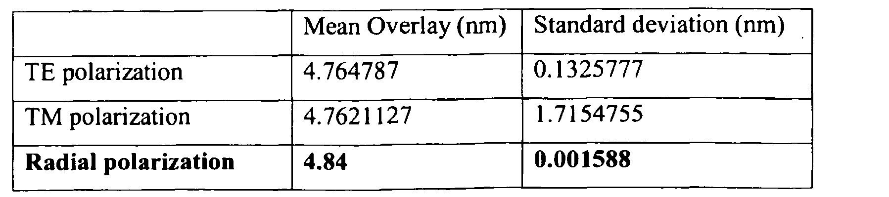
Table 2:Table 2:

As can be seen from the results, in Table 1, the mean overlay result of 4.84nm is closer to the actual overlay of 5nm, than either linearly polarized radiation beams show. Furthermore, the values for each pixel in the pixel maps shown in Figures 10, 11 and 12 are also smoother, indicating that the standard deviation is smaller and so filters are not required to remove noise. Table 2 also shows a more accurate mean overlay result for radial polarization rather than linear polarization, again with a smaller standard deviation.As can be seen from the results, in Table 1, the mean overlay result or 4.84 nm is closer to the actual overlay or 5 nm, than either linearly polarized radiation beams show. Furthermore, the values for each pixel in the pixel maps shown in Figures 10, 11 and 12 are also smoother, indicating that the standard deviation is narrower and so filters are not required to remove noise. Table 2 also shows a more accurate mean overlay result for radial polarization rather than linear polarization, again with a smaller standard deviation.
The images in Figures 10, 11 and 12 show only the free pixel map (first free order) of the first diffraction order with the zeroth diffraction order such that it is specifically only the parts of the rings of Figure 4b that are within the zeroth diffraction order ring that are measured.The images in Figures 10, 11 and 12 show only the free pixel map (first free order) or the first diffraction order with the zeroth diffraction order such that it is specifically only the parts of the rings or Figure 4b that are within the zeroth diffraction order ring that are measured.
Looking more closely at Figures 10, 11 and 12, it can be seen from Figure 10 that the shade of the overlay image appears somewhere between 4 and 5nm at point P. On Figure 11, the range of the scale is closer to 5 and the shade of the image, labeled as Q, is somewhere between 4.95 and 5nm. However, a much more accurate mapping can be created using radially polarized light because the standard deviation is much smaller. The standard deviation is therefore shown on the scale to the right of the overlay pixel map and it can be seen that shade of the overlay is at a point labeled R on Figure 12, which is between 4.98 and 4.99nm.Looking more closely at Figures 10, 11 and 12, it can be seen from Figure 10 that the shade of the overlay image appears somewhere between 4 and 5nm at point P. On Figure 11, the range of the scale is closer to 5 and the shade of the image, labeled as Q, is somewhere between 4.95 and 5nm. However, a much more accurate mapping can be created using radially polarized light because the standard deviation is much narrower. The standard deviation is therefore shown on the scale to the right of the overlay pixel map and it can be seen that shade of the overlay is at a point labeled R on Figure 12, which is between 4.98 and 4.99nm.
As can be seen from these results of the simulations, radially polarized light gives a smoother distribution of overly values for each pixel, leading to a small standard deviation and therefore a closer result to the actually overlay result. Many simulations have been carried out using other models of the stack or pattern (shown in Figure 9) and different overlay values including large overlay values up to 30nm, as well as different wavelengths of measurement radiation. In every case, significant improvement of the standard deviation has been observed and the mean overlay value has been seen to been closer to the real overlay.As can be seen from these results of the simulations, radially polarized light gives a smoother distribution of overly values for each pixel, leading to a small standard deviation and therefore a closer result to the actually overlay result. Many simulations have been carried out using other models of the stack or pattern (shown in Figure 9) and different overlay values including large overlay values up to 30 nm, as well as different wavelengths or measurement radiation. In every case, significant improvement of the standard deviation has been observed and the mean overlay value has been seen to be closer to the real overlay.
Although specific reference may be made in this text to the use of lithographic apparatus in the manufacture of ICs, it should be understood that the lithographic apparatus described herein may have other applications, such as the manufacture of integrated optical systems, guidance and detection patterns for magnetic domain memories, flat-panel displays, liquid-crystal displays (LCDs), thin film magnetic heads, etc.. The skilled artisan will appreciate that, in the context of such alternative applications, any use of the terms "wafer" or "die" herein may be considered as synonymous with the more general terms "substrate" or "target portion", respectively. The substrate referred to herein may be processed, before or after exposure, in for example a track (a tool that typically applies a layer of resist to a substrate and develops the exposed resist), a metrology tool and/or an inspection tool. Where applicable, the disclosure herein may be applied to such and other substrate processing tools. Further, the substrate may be processed more than once, for example in order to create a multi-layer IC, so that the term substrate used herein may also refer to a substrate that already contains multiple processed layers.Although specific reference may be made in this text to the use of lithographic apparatus in the manufacture of ICs, it should be understood that the lithographic apparatus described may have other applications, such as the manufacture of integrated optical systems, guidance and detection patterns for magnetic domain memories, flat-panel displays, liquid-crystal displays (LCDs), thin film magnetic heads, etc .. The skilled artisan will appreciate that, in the context of such alternative applications, any use of the terms "wafer" or " those "may be considered as synonymous with the more general terms" substrate "or" target portion ", respectively. The substrate referred to may be processed, before or after exposure, in for example a track (a tool that typically applies to a layer of resist to a substrate and develops the exposed resist), a metrology tool and / or an inspection tool. Where applicable, the disclosure may be applied to such and other substrate processing tools. Further, the substrate may be processed more than once, for example in order to create a multi-layer IC, so the term substrate used may also refer to a substrate that already contains multiple processed layers.
Although specific reference may have been made above to the use of embodiments of the invention in the context of optical lithography, it will be appreciated that the invention may be used in other applications, for example imprint lithography, and where the context allows, is not limited to optical lithography. In imprint lithography a topography in a patterning device defines the pattern created on a substrate. The topography of the patterning device may be pressed into a layer of resist supplied to the substrate whereupon the resist is cured by applying electromagnetic radiation, heat, pressure or a combination thereof. The patterning device is moved out of the resist leaving a pattern in it after the resist is cured.Although specific reference may have been made above to the use of the invention in the context of optical lithography, it will be appreciated that the invention may be used in other applications, for example imprint lithography, and where the context allows, is not limited to optical lithography. In imprint lithography a topography in a patterning device the pattern created on a substrate. The topography of the patterning device may be pressed into a layer or resist supplied to the substrate whereupon the resist is cured by applying electromagnetic radiation, heat, pressure or a combination thereof. The patterning device is moved out of the resist leaving a pattern in it after the resist is cured.
The terms "radiation" and "beam" used herein encompass all types of electromagnetic radiation, including ultraviolet (UV) radiation (e.g. having a wavelength of or about 365, 355, 248, 193, 157 or 126 nm) and extreme ultra-violet (EUV) radiation (e.g. having a wavelength in the range of 5-20 nm), as well as particle beams, such as ion beams or electron beams.The terms "radiation" and "beam" used include and compass all types of electromagnetic radiation, including ultraviolet (UV) radiation (eg having a wavelength of or about 365, 355, 248, 193, 157 or 126 nm) and extreme ultra-violet (EUV) radiation (eg having a wavelength in the range of 5-20 nm), as well as particle beams, such as ion beams or electron beams.
The term "lens", where the context allows, may refer to any one or combination of various types of optical components, including refractive, reflective, magnetic, electromagnetic and electrostatic optical components.The term "lens", where the context allows, may refer to any one or combination of various types of optical components, including refractive, reflective, magnetic, electromagnetic and electrostatic optical components.
While specific embodiments of the invention have been described above, it will be appreciated that the invention may be practiced otherwise than as described. For example, the invention may take the form of a computer program containing one or more sequences of machine-readable instructions describing a method as disclosed above, or a data storage medium (e.g. semiconductor memory, magnetic or optical disk) having such a computer program stored therein.While specific expired or the invention have been described above, it will be appreciated that the invention may be practiced otherwise than as described. For example, the invention may take the form of a computer program containing one or more sequences of machine-readable instructions describing a method as disclosed above, or a data storage medium (eg semiconductor memory, magnetic or optical disk) having such a computer program stored therein.
The descriptions above are intended to be illustrative, not limiting. Thus, it will be apparent to one skilled in the art that modifications may be made to the invention as described without departing from the scope of the clauses set out below. Other aspects of the invention are set out as in the following clauses: 1. A scatterometer configured to measure a property of a substrate, comprising: a radiation source configured to provide a radiation beam; a high numerical aperture lens; and a detector configured to detect an angle-resolved spectrum of the radiation beam reflected at a plurality of angles from a surface of the substrate, wherein the radiation source is configured to radially polarize the radiation beam. 2. A scatterometer according to clause 1, wherein the radiation source comprises a liquid nematic cell configured to polarize the radiation beam 3. A scatterometer according to clause 1, further comprising: an optical system configured to focus the radially polarized radiation beam to a focal spot with a diameter of up to about 200nm. 4. A scatterometer according to clause 1, configured to measure an overlay of a first layer on a substrate with respect to a second layer superimposed onto the first layer, wherein: the detector is configured to detect at least the zeroth and first orders of the angle-resolved spectrum of the radially polarized radiation beam having been reflected from the superimposed first and second layers and to output an image of the respective intensities of the zeroth, -1 and +1 diffraction orders, a parameter of the image indicating the extent of the overlay. 5. A scatterometer according to clause 4, wherein the parameter of the image indicating the extent of the overlay comprises a value on a color- or gray-scale pixel image. 6. The scatterometer according to clause 1, wherein the property of the substrate is further measured by measuring, in the pupil plane of the high numerical aperture lens, a property of the reflected spectrum at a plurality of wavelengths simultaneously. 7. The scatterometer according to clause 1, wherein the numerical aperture of the lens is at least about 0.9. 8. The scatterometer according to clause 1, further comprising: a space between the substrate and the high numerical aperture lens containing a liquid. 9. The scatterometer according to clause 1, wherein the radiation source comprises: a polarizer configured to radially polarize the radiation beam. 10. The scatterometer according to clause 1, wherein a critical dimension of a structure on the substrate is measured by measuring features in the reflected spectrum, the features being comparable to a library of predetermined features associated with known critical dimensions. 11. The scatterometer according to clause 1, wherein the features in the reflected spectrum include asymmetry. 12. A method of measuring a property of a substrate, comprising providing a radiation beam; printing a pattern onto a substrate; and measuring, in the pupil plane of a high numerical aperture lens, a reflected spectrum of the pattern, wherein the method further comprises: radially polarizing the radiation beam. 13. The method according to clause 12, wherein measuring the reflected spectrum comprises measuring (a) a property of the reflected spectrum at a plurality of angles, (b) a plurality of wavelengths, or both (a) and (b) simultaneously. 14. The method according to clause 12, wherein the pattern comprises two gratings layered in parallel and misaligned, thereby creating an overlay of one grating with respect to the other; the measuring of the reflected spectrum of the gratings is carried out using a scatterometer; and the extent of the overlay is derived from the asymmetry in the reflected spectrum. 15. A lithographic apparatus comprising: an illumination optical system arranged to illuminate a pattern; a projection optical system arranged to project an image of the pattern on to a substrate; and an angularly resolved scatterometer configured to measure a property of the substrate, the scatterometer comprising: a radiation source configured to provide a radiation beam; a high numerical aperture lens; and a detector configured to detect an angle-resolved spectrum of the radiation beam reflected at a plurality of angles from a surface of the substrate, wherein the radiation source is configured to radially polarize the radiation beam. 16. A lithographic cell comprising: a coater arranged to coat substrates with a radiation sensitive layer; a lithographic apparatus arranged to expose images onto the radiation sensitive layer of substrates coated by the coater; a developer arranged to develop images exposed by the lithographic apparatus; and an angularly resolved scatterometer configured to measure a property of a substrate, the scatterometer comprising: a radiation source configured to provide a radiation beam; a high numerical aperture lens; and a detector configured to detect an angle-resolved spectrum of the radiation beam reflected at a plurality of angles from a surface of the substrate, wherein the radiation source is configured to radially polarize the radiation beam. 17. A device manufacturing method comprising: forming a pattern on a substrate using a lithographic apparatus; and determining a value related to a parameter of the pattern printed by: providing a radiation beam; printing a pattern onto the substrate; and measuring, in the pupil plane of a high numerical aperture lens, a reflected spectrum of the pattern, the reflected spectrum being created by the reflection of a radially polarized radiation beam from the pattern on the substrate.The descriptions above are intended to be illustrative, not limiting. Thus, it will be apparent to one skilled in the art that modifications may be made to the invention as described without departing from the scope or the clauses set out below. Other aspects of the invention are set out as in the following clauses: 1. A scatterometer configured to measure a property of a substrate, including: a radiation source configured to provide a radiation beam; a high numerical aperture lens; and a detector configured to detect an angle-resolved spectrum of the radiation beam reflected on a variety of angles from a surface of the substrate, the radiation source is configured to radially polarize the radiation beam. 2. A scatterometer according to clause 1, including the radiation source comprises a liquid nematic cell configured to polarize the radiation beam 3. A scatterometer according to clause 1, further including: an optical system configured to focus the radially polarized radiation beam to a focal spot with a diameter or up to about 200nm. 4. A scatterometer according to clause 1, configured to measure an overlay or a first layer on a substrate with respect to a second layer superimposed on the first layer, namely: the detector is configured to detect at least the zeroth and first orders of the angle-resolved spectrum of the radially polarized radiation beam having been reflected from the superimposed first and second layers and to output an image of the respective intensities of the zeroth, -1 and +1 diffraction orders, a parameter of the image indicating the extent of the overlay. 5. A scatterometer according to clause 4, where the parameter of the image indicates the extent of the overlay includes a value on a color or gray-scale pixel image. 6. The scatterometer according to clause 1, the property of the substrate is further measured by measuring, in the pupil plane of the high numerical aperture lens, a property of the reflected spectrum at a multiple of wavelengths simultaneously. 7. The scatterometer according to clause 1, the numerical aperture of the lens is at least about 0.9. 8. The scatterometer according to clause 1, further including: a space between the substrate and the high numerical aperture lens containing a liquid. 9. The scatterometer according to clause 1, including the radiation source comprises: a polarizer configured to radially polarize the radiation beam. 10. The scatterometer according to clause 1, where a critical dimension or a structure on the substrate is measured by measuring features in the reflected spectrum, the features being comparable to a library or predetermined features associated with known critical dimensions. 11. The scatterometer according to clause 1, the features in the reflected spectrum include asymmetry. 12. A method of measuring a property or a substrate, including a radiation beam; printing a pattern onto a substrate; and measuring, in the pupil plane of a high numerical aperture lens, a reflected spectrum of the pattern, in the method further comprises: radially polarizing the radiation beam. 13. The method according to clause 12, measuring the reflected spectrum comprises measuring (a) a property of the reflected spectrum at a variety of angles, (b) a variety of wavelengths, or both (a) and (b) simultaneously. 14. The method according to clause 12, the pattern comprising two gratings layered in parallel and misaligned, creating an overlay or one grating with respect to the other; the measuring of the reflected spectrum of the gratings is carried out using a scatterometer; and the extent of the overlay is derived from the asymmetry in the reflected spectrum. 15. A lithographic apparatus including: an illumination optical system arranged to illuminate a pattern; a projection optical system arranged to project an image of the pattern on a substrate; and an angularly resolved scatterometer configured to measure a property of the substrate, the scatterometer including: a radiation source configured to provide a radiation beam; a high numerical aperture lens; and a detector configured to detect an angle-resolved spectrum of the radiation beam reflected on a variety of angles from a surface of the substrate, the radiation source is configured to radially polarize the radiation beam. 16. A lithographic cell comprising: a coater arranged to coat substrates with a radiation sensitive layer; a lithographic apparatus arranged to expose images onto the radiation sensitive layer or substrates coated by the coater; a developer arranged to develop images exposed by the lithographic apparatus; and an angularly resolved scatterometer configured to measure a property of a substrate, the scatterometer including: a radiation source configured to provide a radiation beam; a high numerical aperture lens; and a detector configured to detect an angle-resolved spectrum of the radiation beam reflected on a variety of angles from a surface of the substrate, the radiation source is configured to radially polarize the radiation beam. 17. A device manufacturing method including: forming a pattern on a substrate using a lithographic apparatus; and determining a value related to a parameter of the pattern printed by: providing a radiation beam; printing a pattern onto the substrate; and measuring, in the pupil plane of a high numerical aperture lens, a reflected spectrum of the pattern, the reflected spectrum being created by the reflection of a radially polarized radiation beam from the pattern on the substrate.
Claims (1)
Applications Claiming Priority (2)
| Application Number | Priority Date | Filing Date | Title |
|---|---|---|---|
| US99635607P | 2007-11-13 | 2007-11-13 | |
| US99635607 | 2007-11-13 |
Publications (1)
| Publication Number | Publication Date |
|---|---|
| NL1036123A1 true NL1036123A1 (en) | 2009-05-14 |
Family
ID=41491592
Family Applications (1)
| Application Number | Title | Priority Date | Filing Date |
|---|---|---|---|
| NL1036123A NL1036123A1 (en) | 2007-11-13 | 2008-10-28 | Inspection method and apparatus, lithographic apparatus, lithographic processing cell and device manufacturing method. |
Country Status (3)
| Country | Link |
|---|---|
| US (1) | US8553227B2 (en) |
| JP (1) | JP2009200466A (en) |
| NL (1) | NL1036123A1 (en) |
Families Citing this family (82)
| Publication number | Priority date | Publication date | Assignee | Title |
|---|---|---|---|---|
| JP5545782B2 (en) * | 2009-07-31 | 2014-07-09 | エーエスエムエル ネザーランズ ビー.ブイ. | Lithographic apparatus focus measurement method, scatterometer, lithography system, and lithography cell |
| NL2005266A (en) * | 2009-10-28 | 2011-05-02 | Asml Netherlands Bv | Imprint lithography. |
| TWI401549B (en) * | 2009-12-02 | 2013-07-11 | Ind Tech Res Inst | Method for designing two dimensional overlay array target and method and system for measureing overlay error using the same |
| FR2962804B1 (en) | 2010-07-19 | 2014-04-18 | Horiba Jobin Yvon Sas | POLARIMETRIC MEASUREMENT DEVICE AND METHOD WITH MICROSCOPIC RESOLUTION, POLARIMETRY ACCESSORY FOR MICROSCOPE, ELLIPSO-MICROSCOPE AND MICROSCOPE WITH ELLIPSOMETRIC CONTRAST |
| AU2011201885A1 (en) * | 2010-07-21 | 2012-02-09 | Agilent Technologies Australia (M) Pty Ltd | Apparatus for absolute variable angle specular reflectance measurements |
| US8890073B2 (en) | 2011-03-28 | 2014-11-18 | Northrop Grumman Guidance And Electronics Company, Inc. | Systems and methods for detecting and/or identifying materials based on electromagnetic radiation |
| NL2009294A (en) * | 2011-08-30 | 2013-03-04 | Asml Netherlands Bv | Method and apparatus for determining an overlay error. |
| US9466100B2 (en) | 2012-06-06 | 2016-10-11 | Kla-Tencor Corporation | Focus monitoring method using asymmetry embedded imaging target |
| US9093458B2 (en) * | 2012-09-06 | 2015-07-28 | Kla-Tencor Corporation | Device correlated metrology (DCM) for OVL with embedded SEM structure overlay targets |
| US9619878B2 (en) * | 2013-04-16 | 2017-04-11 | Kla-Tencor Corporation | Inspecting high-resolution photolithography masks |
| CN104423173B (en) * | 2013-08-27 | 2016-09-28 | 上海微电子装备有限公司 | Alignment measurement apparatus and method |
| US10365230B1 (en) | 2014-03-19 | 2019-07-30 | Kla-Tencor Corporation | Scatterometry overlay based on reflection peak locations |
| KR102135999B1 (en) * | 2014-03-20 | 2020-07-21 | 케이엘에이 코포레이션 | Compressive sensing with illumination patterning |
| EP3009877A1 (en) | 2014-10-15 | 2016-04-20 | Optosys SA | Device for emission of polarized light and its detection |
| US9970863B2 (en) | 2015-02-22 | 2018-05-15 | Kla-Tencor Corporation | Optical metrology with reduced focus error sensitivity |
| NL2017300A (en) * | 2015-08-27 | 2017-03-01 | Asml Netherlands Bv | Method and apparatus for measuring a parameter of a lithographic process, substrate and patterning devices for use in the method |
| TWI656409B (en) * | 2015-09-09 | 2019-04-11 | 美商克萊譚克公司 | A new method based on the introduction of auxiliary electromagnetic field to superimpose first-order scattering measurement |
| US10393514B2 (en) | 2015-10-08 | 2019-08-27 | Asml Netherlands B.V. | Topography measurement system |
| US10546790B2 (en) * | 2016-03-01 | 2020-01-28 | Asml Netherlands B.V. | Method and apparatus to determine a patterning process parameter |
| US10983005B2 (en) * | 2016-12-15 | 2021-04-20 | Taiwan Semiconductor Manufacturing Co., Ltd. | Spectroscopic overlay metrology |
| WO2018188891A1 (en) * | 2017-04-14 | 2018-10-18 | Asml Netherlands B.V. | Method of measuring |
| CN110799903B (en) | 2017-06-20 | 2021-11-16 | Asml荷兰有限公司 | Determining an edge roughness parameter |
| WO2019020484A1 (en) | 2017-07-25 | 2019-01-31 | Asml Netherlands B.V. | Method for parameter determination and apparatus thereof |
| IL312300B2 (en) | 2017-09-01 | 2025-07-01 | Asml Netherlands Bv | Optical systems, metrology instruments and related methods |
| IL273145B2 (en) | 2017-09-11 | 2024-03-01 | Asml Netherlands Bv | Lithographic processes in meteorology |
| EP3457211A1 (en) | 2017-09-13 | 2019-03-20 | ASML Netherlands B.V. | A method of aligning a pair of complementary diffraction patterns and associated metrology method and apparatus |
| EP3474074A1 (en) | 2017-10-17 | 2019-04-24 | ASML Netherlands B.V. | Scatterometer and method of scatterometry using acoustic radiation |
| EP3480659A1 (en) | 2017-11-01 | 2019-05-08 | ASML Netherlands B.V. | Estimation of data in metrology |
| KR102648880B1 (en) | 2017-11-07 | 2024-03-15 | 에이에스엠엘 네델란즈 비.브이. | Metrology apparatus and a method of determining a characteristic of interest |
| US10473460B2 (en) * | 2017-12-11 | 2019-11-12 | Kla-Tencor Corporation | Overlay measurements of overlapping target structures based on symmetry of scanning electron beam signals |
| IL275640B2 (en) | 2017-12-28 | 2025-05-01 | Asml Netherlands Bv | A metrology apparatus for and a method of determining a characteristic of interest of a structure on a substrate |
| EP3570109A1 (en) | 2018-05-14 | 2019-11-20 | ASML Netherlands B.V. | Illumination source for an inspection apparatus, inspection apparatus and inspection method |
| CN118068655A (en) | 2018-06-13 | 2024-05-24 | Asml荷兰有限公司 | Measuring apparatus |
| EP3582009A1 (en) | 2018-06-15 | 2019-12-18 | ASML Netherlands B.V. | Reflector and method of manufacturing a reflector |
| EP3611569A1 (en) | 2018-08-16 | 2020-02-19 | ASML Netherlands B.V. | Metrology apparatus and photonic crystal fiber |
| KR20210040134A (en) | 2018-09-04 | 2021-04-12 | 에이에스엠엘 네델란즈 비.브이. | Measuring device |
| EP3627226A1 (en) | 2018-09-20 | 2020-03-25 | ASML Netherlands B.V. | Optical system, metrology apparatus and associated method |
| EP3629086A1 (en) * | 2018-09-25 | 2020-04-01 | ASML Netherlands B.V. | Method and apparatus for determining a radiation beam intensity profile |
| US11087065B2 (en) | 2018-09-26 | 2021-08-10 | Asml Netherlands B.V. | Method of manufacturing devices |
| KR102598600B1 (en) | 2018-10-24 | 2023-11-06 | 에이에스엠엘 네델란즈 비.브이. | Optical fiber and its production method |
| EP3650941A1 (en) | 2018-11-12 | 2020-05-13 | ASML Netherlands B.V. | Method of determining the contribution of a processing apparatus to a substrate parameter |
| CN113039487B (en) | 2018-11-16 | 2024-05-14 | Asml荷兰有限公司 | Method for monitoring a lithographic apparatus |
| CN113168115B (en) | 2018-12-03 | 2024-12-13 | Asml荷兰有限公司 | Method of manufacturing device |
| EP3696606A1 (en) | 2019-02-15 | 2020-08-19 | ASML Netherlands B.V. | A metrology apparatus with radiation source having multiple broadband outputs |
| EP3703114A1 (en) | 2019-02-26 | 2020-09-02 | ASML Netherlands B.V. | Reflector manufacturing method and associated reflector |
| EP3702840A1 (en) | 2019-03-01 | 2020-09-02 | ASML Netherlands B.V. | Alignment method and associated metrology device |
| EP3705942A1 (en) | 2019-03-04 | 2020-09-09 | ASML Netherlands B.V. | Hollow-core photonic crystal fiber based optical component for broadband radiation generation |
| KR102636261B1 (en) | 2019-03-25 | 2024-02-13 | 에이에스엠엘 네델란즈 비.브이. | Frequency expansion device and method |
| EP3948373A1 (en) | 2019-04-03 | 2022-02-09 | ASML Netherlands B.V. | Optical fiber |
| EP3739389A1 (en) | 2019-05-17 | 2020-11-18 | ASML Netherlands B.V. | Metrology tools comprising aplanatic objective singlet |
| US12164233B2 (en) | 2019-06-17 | 2024-12-10 | Asml Netherlands B.V. | Metrology method and apparatus for of determining a complex-valued field |
| WO2020254138A1 (en) | 2019-06-21 | 2020-12-24 | Asml Netherlands B.V. | Mounted hollow-core fibre arrangement |
| EP3758168A1 (en) | 2019-06-25 | 2020-12-30 | ASML Netherlands B.V. | Hollow-core photonic crystal fiber based optical component for broadband radiation generation |
| EP3611567A3 (en) | 2019-07-23 | 2020-05-13 | ASML Netherlands B.V. | Improvements in metrology targets |
| WO2021013611A1 (en) | 2019-07-24 | 2021-01-28 | Asml Netherlands B.V. | Radiation source |
| CN114207432B (en) | 2019-08-14 | 2025-06-13 | Asml荷兰有限公司 | Method and metrology tool for determining information about a target structure and cantilever probe |
| EP3783439A1 (en) | 2019-08-22 | 2021-02-24 | ASML Netherlands B.V. | Metrology device and detection apparatus therefor |
| EP3786713A1 (en) | 2019-09-02 | 2021-03-03 | ASML Netherlands B.V. | Metrology method and device for determining a complex-valued field |
| KR102718090B1 (en) | 2019-09-02 | 2024-10-18 | 에이에스엠엘 네델란즈 비.브이. | Mode control of broadband light sources based on photonic crystal fibers |
| IL290406B2 (en) | 2019-09-03 | 2025-08-01 | Asml Netherlands Bv | Assembly for collecting broadband radiation |
| CN114514465B (en) | 2019-09-18 | 2025-03-28 | Asml荷兰有限公司 | Improved broadband radiation generation in hollow core optical fibers |
| EP3796089A1 (en) | 2019-09-18 | 2021-03-24 | ASML Holding N.V. | A method for filtering an image and associated metrology apparatus |
| EP3809190A1 (en) | 2019-10-14 | 2021-04-21 | ASML Netherlands B.V. | Method and apparatus for coherence scrambling in metrology applications |
| US12044951B2 (en) | 2019-10-17 | 2024-07-23 | Asml Netherlands B.V. | Illumination source and associated metrology apparatus |
| WO2021078690A1 (en) | 2019-10-24 | 2021-04-29 | Asml Netherlands B.V. | Hollow-core photonic crystal fiber based optical component for broadband radiation generation |
| EP3816721A1 (en) | 2019-10-29 | 2021-05-05 | ASML Netherlands B.V. | Method and apparatus for efficient high harmonic generation |
| KR20220066963A (en) | 2019-11-05 | 2022-05-24 | 에이에스엠엘 네델란즈 비.브이. | Measuring method and measuring device |
| DK3819267T3 (en) | 2019-11-07 | 2022-08-29 | Asml Netherlands Bv | Method for manufacturing a capillary for a hollow core photonic crystal fiber |
| EP3839632A1 (en) | 2019-12-20 | 2021-06-23 | ASML Netherlands B.V. | Method for determining a measurement recipe and associated apparatuses |
| WO2021144093A1 (en) | 2020-01-15 | 2021-07-22 | Asml Netherlands B.V. | Method, assembly, and apparatus for improved control of broadband radiation generation |
| EP3879343A1 (en) | 2020-03-11 | 2021-09-15 | ASML Netherlands B.V. | Metrology measurement method and apparatus |
| EP3889681A1 (en) | 2020-03-31 | 2021-10-06 | ASML Netherlands B.V. | An assembly including a non-linear element and a method of use thereof |
| EP3913429A1 (en) | 2020-05-19 | 2021-11-24 | ASML Netherlands B.V. | A supercontinuum radiation source and associated metrology devices |
| IL320838A (en) | 2020-07-08 | 2025-07-01 | Asml Netherlands Bv | Broadband radiation generator based on hollow fibers with extended fiber life |
| EP3958052A1 (en) | 2020-08-20 | 2022-02-23 | ASML Netherlands B.V. | Metrology method for measuring an exposed pattern and associated metrology apparatus |
| KR20230061399A (en) | 2020-09-03 | 2023-05-08 | 에이에스엠엘 네델란즈 비.브이. | Broadband radiation generator based on hollow-core photonic crystal fibers |
| US12411421B2 (en) | 2020-11-30 | 2025-09-09 | Asml Netherlands B.V. | Metrology apparatus based on high harmonic generation and associated method |
| JP7739429B2 (en) | 2020-12-10 | 2025-09-16 | エーエスエムエル ネザーランズ ビー.ブイ. | Broadband radiation generator based on hollow-core photonic crystal fiber |
| EP4560400A1 (en) | 2023-11-27 | 2025-05-28 | Stichting Nederlandse Wetenschappelijk Onderzoek Instituten | Method for determining an optical property of a multi-layer structure |
| WO2025131523A1 (en) | 2023-12-21 | 2025-06-26 | Asml Netherlands B.V. | Metrology method for a digital holographic microscope and associated computer program |
| WO2025171992A1 (en) | 2024-02-12 | 2025-08-21 | Asml Netherlands B.V. | An illumination and detection arrangement and a method for a metrology arrangement |
| EP4600746A1 (en) | 2024-02-12 | 2025-08-13 | ASML Netherlands B.V. | An illumination and detection arrangement and a method for a metrology arrangement |
Family Cites Families (13)
| Publication number | Priority date | Publication date | Assignee | Title |
|---|---|---|---|---|
| DE19535392A1 (en) | 1995-09-23 | 1997-03-27 | Zeiss Carl Fa | Radial polarization-rotating optical arrangement and microlithography projection exposure system with it |
| US7869057B2 (en) * | 2002-09-09 | 2011-01-11 | Zygo Corporation | Multiple-angle multiple-wavelength interferometer using high-NA imaging and spectral analysis |
| DE10393244B4 (en) * | 2002-09-09 | 2017-09-21 | Zygo Corp. | Interferometric method for ellipsometric, reflectometric and scattered-light analytical measurements, including the characterization of thin-film structures |
| US7139081B2 (en) * | 2002-09-09 | 2006-11-21 | Zygo Corporation | Interferometry method for ellipsometry, reflectometry, and scatterometry measurements, including characterization of thin film structures |
| US7102761B2 (en) | 2003-06-13 | 2006-09-05 | Zygo Corporation | Scanning interferometry |
| KR101099847B1 (en) * | 2004-01-16 | 2011-12-27 | 칼 짜이스 에스엠티 게엠베하 | Polarization-modulating optical element |
| US8270077B2 (en) | 2004-01-16 | 2012-09-18 | Carl Zeiss Smt Gmbh | Polarization-modulating optical element |
| DE602004014338D1 (en) * | 2004-03-08 | 2008-07-24 | Asml Netherlands Bv | Lithographic apparatus with a radial polarizer |
| US7791727B2 (en) * | 2004-08-16 | 2010-09-07 | Asml Netherlands B.V. | Method and apparatus for angular-resolved spectroscopic lithography characterization |
| JP4612849B2 (en) * | 2005-03-01 | 2011-01-12 | キヤノン株式会社 | Exposure method, exposure apparatus, and device manufacturing method |
| EP1744214B1 (en) * | 2005-07-15 | 2010-03-03 | Imec | Methods and systems for improved optical lithographic processing |
| JP2007103835A (en) * | 2005-10-07 | 2007-04-19 | Toshiba Corp | Exposure apparatus and exposure method |
| JP4750525B2 (en) * | 2005-10-14 | 2011-08-17 | キヤノン株式会社 | Exposure method and device manufacturing method |
-
2008
- 2008-10-28 NL NL1036123A patent/NL1036123A1/en active Search and Examination
- 2008-11-06 JP JP2008284915A patent/JP2009200466A/en active Pending
-
2009
- 2009-06-17 US US12/486,449 patent/US8553227B2/en active Active
Also Published As
| Publication number | Publication date |
|---|---|
| US8553227B2 (en) | 2013-10-08 |
| US20100007863A1 (en) | 2010-01-14 |
| JP2009200466A (en) | 2009-09-03 |
Similar Documents
| Publication | Publication Date | Title |
|---|---|---|
| US8553227B2 (en) | Inspection method and apparatus, lithographic apparatus, lithographic processing cell and device manufacturing method | |
| US9128065B2 (en) | Inspection apparatus, lithographic apparatus, lithographic processing cell and inspection method | |
| JP4787232B2 (en) | Measuring method, inspection apparatus, and lithography apparatus | |
| EP1881374B1 (en) | Inspection method and apparatus, lithographic apparatus, lithographic process line and device manufacturing method | |
| US7911612B2 (en) | Inspection method and apparatus, lithographic apparatus, lithographic processing cell and device manufacturing method | |
| TWI405046B (en) | A method of assessing a model, an inspection apparatus and a lithographic apparatus | |
| JP4672704B2 (en) | Method of measuring substrate overlay error, substrate manufacturing method, and inspection apparatus | |
| US7619737B2 (en) | Method of measurement, an inspection apparatus and a lithographic apparatus | |
| TWI640801B (en) | Inspection method and apparatus, lithographic apparatus, lithographic processing cell and device manufacturing method | |
| US9746785B2 (en) | Sub-wavelength segmentation in measurement targets on substrates | |
| US9280065B2 (en) | Inspection apparatus to detect a target located within a pattern for lithography | |
| US8363218B2 (en) | Inspection method and apparatus, lithographic apparatus, lithographic processing cell and device manufacturing method | |
| US9081304B2 (en) | Substrate, an inspection apparatus, and a lithographic apparatus | |
| NL1035874A1 (en) | A method of measuring the overlay error, an inspection apparatus and a lithographic apparatus. | |
| NL1036683A1 (en) | Focus sensor, inspection apparatus, lithographic apparatus and control system. | |
| NL2004688A (en) | Inspection method and apparatus, lithographic apparatus, lithographic processing cell and device manufacturing method. |
Legal Events
| Date | Code | Title | Description |
|---|---|---|---|
| AD1A | A request for search or an international type search has been filed |