KR920003400B1 - Verbund material fuer leiterpltten - Google Patents
Verbund material fuer leiterpltten Download PDFInfo
- Publication number
- KR920003400B1 KR920003400B1 KR1019840008470A KR840008470A KR920003400B1 KR 920003400 B1 KR920003400 B1 KR 920003400B1 KR 1019840008470 A KR1019840008470 A KR 1019840008470A KR 840008470 A KR840008470 A KR 840008470A KR 920003400 B1 KR920003400 B1 KR 920003400B1
- Authority
- KR
- South Korea
- Prior art keywords
- metal
- copper
- resin
- composite
- layer
- Prior art date
Links
Images


Classifications
-
- H—ELECTRICITY
- H05—ELECTRIC TECHNIQUES NOT OTHERWISE PROVIDED FOR
- H05K—PRINTED CIRCUITS; CASINGS OR CONSTRUCTIONAL DETAILS OF ELECTRIC APPARATUS; MANUFACTURE OF ASSEMBLAGES OF ELECTRICAL COMPONENTS
- H05K3/00—Apparatus or processes for manufacturing printed circuits
- H05K3/46—Manufacturing multilayer circuits
-
- H—ELECTRICITY
- H05—ELECTRIC TECHNIQUES NOT OTHERWISE PROVIDED FOR
- H05K—PRINTED CIRCUITS; CASINGS OR CONSTRUCTIONAL DETAILS OF ELECTRIC APPARATUS; MANUFACTURE OF ASSEMBLAGES OF ELECTRICAL COMPONENTS
- H05K3/00—Apparatus or processes for manufacturing printed circuits
- H05K3/38—Improvement of the adhesion between the insulating substrate and the metal
- H05K3/382—Improvement of the adhesion between the insulating substrate and the metal by special treatment of the metal
- H05K3/385—Improvement of the adhesion between the insulating substrate and the metal by special treatment of the metal by conversion of the surface of the metal, e.g. by oxidation, whether or not followed by reaction or removal of the converted layer
-
- H—ELECTRICITY
- H05—ELECTRIC TECHNIQUES NOT OTHERWISE PROVIDED FOR
- H05K—PRINTED CIRCUITS; CASINGS OR CONSTRUCTIONAL DETAILS OF ELECTRIC APPARATUS; MANUFACTURE OF ASSEMBLAGES OF ELECTRICAL COMPONENTS
- H05K2203/00—Indexing scheme relating to apparatus or processes for manufacturing printed circuits covered by H05K3/00
- H05K2203/03—Metal processing
- H05K2203/0315—Oxidising metal
-
- H—ELECTRICITY
- H05—ELECTRIC TECHNIQUES NOT OTHERWISE PROVIDED FOR
- H05K—PRINTED CIRCUITS; CASINGS OR CONSTRUCTIONAL DETAILS OF ELECTRIC APPARATUS; MANUFACTURE OF ASSEMBLAGES OF ELECTRICAL COMPONENTS
- H05K2203/00—Indexing scheme relating to apparatus or processes for manufacturing printed circuits covered by H05K3/00
- H05K2203/11—Treatments characterised by their effect, e.g. heating, cooling, roughening
- H05K2203/1157—Using means for chemical reduction
-
- H—ELECTRICITY
- H05—ELECTRIC TECHNIQUES NOT OTHERWISE PROVIDED FOR
- H05K—PRINTED CIRCUITS; CASINGS OR CONSTRUCTIONAL DETAILS OF ELECTRIC APPARATUS; MANUFACTURE OF ASSEMBLAGES OF ELECTRICAL COMPONENTS
- H05K3/00—Apparatus or processes for manufacturing printed circuits
- H05K3/46—Manufacturing multilayer circuits
- H05K3/4611—Manufacturing multilayer circuits by laminating two or more circuit boards
-
- Y—GENERAL TAGGING OF NEW TECHNOLOGICAL DEVELOPMENTS; GENERAL TAGGING OF CROSS-SECTIONAL TECHNOLOGIES SPANNING OVER SEVERAL SECTIONS OF THE IPC; TECHNICAL SUBJECTS COVERED BY FORMER USPC CROSS-REFERENCE ART COLLECTIONS [XRACs] AND DIGESTS
- Y10—TECHNICAL SUBJECTS COVERED BY FORMER USPC
- Y10T—TECHNICAL SUBJECTS COVERED BY FORMER US CLASSIFICATION
- Y10T428/00—Stock material or miscellaneous articles
- Y10T428/12—All metal or with adjacent metals
- Y10T428/12431—Foil or filament smaller than 6 mils
- Y10T428/12438—Composite
-
- Y—GENERAL TAGGING OF NEW TECHNOLOGICAL DEVELOPMENTS; GENERAL TAGGING OF CROSS-SECTIONAL TECHNOLOGIES SPANNING OVER SEVERAL SECTIONS OF THE IPC; TECHNICAL SUBJECTS COVERED BY FORMER USPC CROSS-REFERENCE ART COLLECTIONS [XRACs] AND DIGESTS
- Y10—TECHNICAL SUBJECTS COVERED BY FORMER USPC
- Y10T—TECHNICAL SUBJECTS COVERED BY FORMER US CLASSIFICATION
- Y10T428/00—Stock material or miscellaneous articles
- Y10T428/12—All metal or with adjacent metals
- Y10T428/12472—Microscopic interfacial wave or roughness
-
- Y—GENERAL TAGGING OF NEW TECHNOLOGICAL DEVELOPMENTS; GENERAL TAGGING OF CROSS-SECTIONAL TECHNOLOGIES SPANNING OVER SEVERAL SECTIONS OF THE IPC; TECHNICAL SUBJECTS COVERED BY FORMER USPC CROSS-REFERENCE ART COLLECTIONS [XRACs] AND DIGESTS
- Y10—TECHNICAL SUBJECTS COVERED BY FORMER USPC
- Y10T—TECHNICAL SUBJECTS COVERED BY FORMER US CLASSIFICATION
- Y10T428/00—Stock material or miscellaneous articles
- Y10T428/12—All metal or with adjacent metals
- Y10T428/12493—Composite; i.e., plural, adjacent, spatially distinct metal components [e.g., layers, joint, etc.]
- Y10T428/12535—Composite; i.e., plural, adjacent, spatially distinct metal components [e.g., layers, joint, etc.] with additional, spatially distinct nonmetal component
- Y10T428/12556—Organic component
- Y10T428/12569—Synthetic resin
-
- Y—GENERAL TAGGING OF NEW TECHNOLOGICAL DEVELOPMENTS; GENERAL TAGGING OF CROSS-SECTIONAL TECHNOLOGIES SPANNING OVER SEVERAL SECTIONS OF THE IPC; TECHNICAL SUBJECTS COVERED BY FORMER USPC CROSS-REFERENCE ART COLLECTIONS [XRACs] AND DIGESTS
- Y10—TECHNICAL SUBJECTS COVERED BY FORMER USPC
- Y10T—TECHNICAL SUBJECTS COVERED BY FORMER US CLASSIFICATION
- Y10T428/00—Stock material or miscellaneous articles
- Y10T428/12—All metal or with adjacent metals
- Y10T428/12493—Composite; i.e., plural, adjacent, spatially distinct metal components [e.g., layers, joint, etc.]
- Y10T428/12771—Transition metal-base component
- Y10T428/12861—Group VIII or IB metal-base component
- Y10T428/12903—Cu-base component
- Y10T428/1291—Next to Co-, Cu-, or Ni-base component
Abstract
내용 없음.No content.
Description
제1도는 본원 발명의 일실시예에 의한 금속과 수지와의 복합체의 단면모식도.1 is a schematic cross-sectional view of a composite of a metal and a resin according to an embodiment of the present invention.
제2도는 전해 환원장치의 원리설명도.2 is a schematic diagram illustrating the principle of the electrolytic reduction apparatus.
제3도는 전해 환원법에 의한 금속석출의 설명도.3 is an explanatory diagram of metal precipitation by the electrolytic reduction method.
제4도는 컬러아날라이저의 광학계통도.4 is an optical system diagram of a color analyzer.
제5도는 전해 환원막의 접착특성도.5 is an adhesive characteristic of the electrolytic reduction film.
제6도는 전해 환원막과 그 이전의 화학적 산화처리막과의 내염산 특성도.6 is a hydrochloric acid resistant characteristic of the electrolytic reduction film and the previous chemical oxidation treatment film.
제7도는 표면반사 특성도.7 is a surface reflection characteristic diagram.
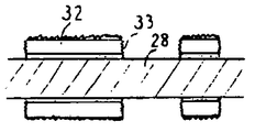
제8도는 프린트판 형성의 공정도.8 is a process chart for forming a printed plate.
제9도는 다층판 형성의 공정도.9 is a process chart of forming a multilayer plate.
* 도면의 주요부분에 대한 부호의 설명* Explanation of symbols for main parts of the drawings
1 : 본바탕 금속층 2 : 전해 환원 금속층DESCRIPTION OF SYMBOLS 1: Bonded metal layer 2: Electrolytic reduction metal layer
3 : 수지층 4 : 제1의 요철부3: resin layer 4: first uneven portion
5 : 제2의 요철부 6 : 시료편5: 2nd uneven part 6: sample piece
7 : 대향극 8 : 전해액7: counter electrode 8: electrolyte
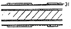
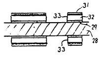
10 : 전해조 28 : 유리섬유강화수지판10
29 : 동박 30, 33 : 동산화막29:
31 : 드라이필름 32 : 동31: dry film 32: copper
34 : 프리프레그34: prepreg
본원 발명은 금속과 수지와의 복합체 및 그 제조방법에 관한 것이며, 특히 프린트판용 기판에의 적용에 적합한 금속과 수지와의 복합체 및 그 제조방법에 관한 것이다.The present invention relates to a composite of a metal and a resin and a method for producing the same, and more particularly, to a composite of a metal and a resin suitable for application to a substrate for a printed plate and a method of producing the same.
종래, 금속과 수지와의 접착에 관해, 수지와의 접착력을 높이기 위해 금속의 표면처리법으로서, 여러가지 방법이 검토되어 왔다. 예를 들어 기계적 또는 산성액중에 있어서, 산화제에 의해 금속의 표면을 에칭하고, 산화한 다음, 자주 알칼리성의 액중에서 또는 액이 산성일지라도, 금속의 표면이 반응에 의해 pH가 높아지는 것을 이용하여, 금속표면상에 산화막을 형성하고, 그 산화막을 통해, 금속과 수지를 접착시키는 방법이 있다. 구체적으로는 예를 들어 동에 대해서는 산성액으로서 염화제 2동과 염산을 포함하는 수용액을 사용하여, 에칭에 의해 금속동 표면을 조화(粗化)한 다음, 아염소산, 인산, 가성소오다를 포함하는 알칼리성의 액에 의해, 동표면에 동의 산화막을 형성하고, 이 산화막을 통해 수지와 실온하에서, 또는 가열하며, 다시 가열, 가압에 의해 접착한다. 또, 금속표면상에 산화막을 형성하는 방법으로서는 과망산칼리와 가성소오다를 포함하는 액에 의해, 산화처리하는 방법도 있다. 또한 산화막을 형성한느 방법으로서는 자외선조사에 의해, 또는 화염처리 등이 있다. 또, 철을 인산중에 담그면, 철은 인산에 의해 산화되며, 그때 철 표면의 pH는 수소발생에 의해 상승하고, 철의 표면상에 안정된 철의 인산염이 생긴다. 수지는 이들 금속산화물 또는 금속염을 통해, 고온도의 접착력을 갖게끔 된다. 그러나, 이들 금속산화물 또는 금속염은 산에 대해 약하다고 하는 결점을 가지고 있다. 금속-수지복합체는 때때로 산과 접하는 분위기하에서 사용될 경우가 있다. 이때문에 금속-수지복합체는 기계적인 접착강도뿐만 아니라, 화학적으로 안정된 것이 요망되고 있다.Background Art Conventionally, various methods have been studied as a surface treatment method of a metal in order to enhance the adhesive force between the resin and the adhesion between the metal and the resin. For example, in a mechanical or acidic liquid, the surface of the metal is etched and oxidized by an oxidizing agent, and then, often in an alkaline liquid or even if the liquid is acidic, the surface of the metal is raised to pH by reaction. There is a method of forming an oxide film on the surface and adhering a metal and a resin through the oxide film. Specifically, for copper, for example, an aqueous solution containing cupric chloride and hydrochloric acid is used as an acid solution, and the surface of the metal copper is roughened by etching, followed by chlorine acid, phosphoric acid, and sodium hydroxide. A copper oxide film is formed on the copper surface by the alkaline liquid, and the resin and the resin are heated at room temperature or at room temperature, and are further bonded by heating and pressure. As a method of forming an oxide film on a metal surface, there is also a method of oxidizing with a liquid containing caloric permanganate and caustic soda. In addition, the method of forming an oxide film includes ultraviolet irradiation or flame treatment. In addition, when iron is immersed in phosphoric acid, iron is oxidized by phosphoric acid, at which time the pH of the iron surface is increased by hydrogen evolution, and stable iron phosphate is formed on the iron surface. Resin will have high temperature adhesive force through these metal oxides or metal salts. However, these metal oxides or metal salts have the disadvantage of being weak against acids. Metal-resin composites are sometimes used in an atmosphere of acid contact. For this reason, metal-resin composites are desired to be not only mechanically strong but also chemically stable.
그런데 동피막의 밀착성 향상방법으로서 일본국 특개소 56-35497호 공보, 동 57-177593호 공보의 기술이 있다. 모두 동피막을 일단 산화한 후, 고온환원성 분위기하에서 순동의 광택이 나올때까지 산화동을 환원하여 순수한 금속표면을 얻는 기술을 개시하고 있으며, 특히 후자에서는 다결정 미립자를 배제하여, 이 입자에 의한 취약성을 해소하는 것을 개시하고 있다. 즉 미립자가 없는 광택 표면에까지 입힌 동이 척층체로 하면 박리강도를 강하게 하는 것으로 되어 있다. 그러나 어느 인례의 기술도 본원 발명자의 검토에 의하면 아직 밀착력은 충분하다고는 할 수 없다. 또 본원 발명자가 알고 있는 한 아직 금속-수지계면의 내산처리에 관한 유효한 기술은 제안되어 있지 않다.By the way, as a method of improving the adhesiveness of copper film, the technique of Unexamined-Japanese-Patent No. 56-35497 and 57-177593 is mentioned. Both of them disclose a technique of oxidizing copper film once and then reducing copper oxide until the gloss of pure copper is obtained under a high temperature reducing atmosphere to obtain a pure metal surface. Particularly, the latter eliminates polycrystalline fine particles and solves the vulnerability of the particles. It is starting to do. In other words, when copper coated on the gloss surface free of fine particles is used as the chuck layer, the peel strength is increased. However, according to the inventor's examination of any example technology, the adhesive force is not enough. Moreover, as far as the inventors of the present application are aware, no effective technique has yet been proposed for the acid-resistant treatment of the metal-resin interface.
본원 발명의 목적은 수지-금속간의 밀착력에 뛰어나며, 그 계면(즉 금속층)이 내산성이 강한 금속과 수지와의 복합체 및 그 제조방법을 제공하는데 있다.An object of the present invention is to provide a composite of a metal and a resin excellent in adhesion between a resin and a metal, and whose interface (ie, a metal layer) is strong in acid resistance, and a method of manufacturing the same.
본원 첫번째의 발명에 의한 금속과 수지와의 복합체는 외관상 무광택이며, 흑갈색(黑褐色) 내지 흑색의 색상을 나타낼 정도의 표면조도를 갖는 금속층이 이 표면에서 수지층에 밀착하고 있는 것을 특징으로 한다.The composite of the metal and the resin according to the first invention of the present application is matt in appearance, and is characterized in that a metal layer having a surface roughness such as blackish brown to black color is in close contact with the resin layer on this surface.
본원 두번째의 발명에 의한 금속과 수지와의 복합체는 본바탕 금속표면에 형성된 제1의 요철부와, 이 제1의 요철부 표면을 그 요철면에 연해 이 제1의 요철부보다도 얇고 또한 미세한 요철표면으로 덮는 환원금속으로 이루어진 제2의 요철부와, 제2의 요철부의 표면에 밀착하는 수지층을 갖는 것을 특징으로 한다.The composite of the metal and the resin according to the second invention of the present application has a first uneven portion formed on the base metal surface and the surface of the first uneven portion connected to the uneven surface to be thinner and finer than the first uneven portion. It has a 2nd uneven part which consists of a reducing metal covered by the surface, and the resin layer which adheres to the surface of a 2nd uneven part. It is characterized by the above-mentioned.
본원 세번째의 발명에 의한 금속과 수지와의 복합체는 전해 환원에 의해 얻어진 금속층이 이 수지층에 밀착하고 있는 것을 특징으로 한다.In the composite of the metal and the resin according to the third invention of the present application, the metal layer obtained by electrolytic reduction is in close contact with the resin layer.
본원 네번째의 발명에 의한 금속과 수지와의 복합체는 본바탕 금속층과 이 본바탕 금속층상에 설치되는 것으로서 금속산화막의 전해 환원으로 얻어지는 환원 금속층과, 이 환원 금속층상에 밀착하는 수지층을 갖는 것을 특징으로 한다.The composite of the metal and the resin according to the fourth invention of the present application is provided on the base metal layer and the base metal layer, and has a reduced metal layer obtained by electrolytic reduction of the metal oxide film, and a resin layer in close contact with the reduced metal layer. It is done.
본원 다섯번째의 발명에 의한 금속과 수지와의 복합체는 금속산화막 표면에 전기적으로 환원해서 얻어지는 환원금속층을 수지층에 밀착시키는 공정을 포함하는 제법으로 얻어지는 것을 특징으로 한다.The composite of the metal and the resin according to the fifth aspect of the present application is obtained by a manufacturing method including a step of bringing the reduced metal layer obtained by electrically reducing the surface of the metal oxide film into close contact with the resin layer.
본원 여섯번째의 발명에 의한 금속과 수지와의 복합체는 얇은 금속동층을 표면에 갖는 절연판의 금속동층의 표면을 산화처리하여 이 표면에 동산화막을 형성하는 제1공정, 레지스트와의 밀착성이 저하하지 않을 정도로 동산화막을 전해 환원하는 제2공정, 이 전해 환원된 동산화막을 비회로부분에 대해서만 레지스트로 덮는 제3공정, 전해 환원된 동산화막의 레지스트로 덮혀 있지 않은 회로부분에 회로도체로서 필요한 두께로 동을 화학도금에 의해 부착시키는 제4공정, 그런 연후에 레지스트를 제거하여 비회로부분의 금속동층 및 전해 환원된 동산화막을 에칭에 의해 제거하는 제5공정을 포함하는 제법으로 얻어진 절연회로판임을 특징으로 한다.The composite of the metal and the resin according to the sixth invention of the present application oxidizes the surface of the metal copper layer of the insulating plate having a thin copper copper layer on the surface to form a copper oxide film on the surface, and the adhesion to the resist is not deteriorated. The second step of electrolytically reducing the copper oxide film to a degree that is not sufficient, the third step of covering the electrolytically reduced copper oxide film with a resist only for the non-circuit portion, and the thickness required as the circuit conductor in the circuit portion not covered with the resist of the electrolytically reduced copper oxide film. The insulating circuit board obtained by the manufacturing method including the 4th process of attaching furnace copper by chemical plating, and the 5th process of removing a resist after that and removing the metal copper layer of a non-circuit part, and the electrolytically reduced copper oxide film by etching. It features.
본원 일곱번째의 발명에 의한 금속과 수지와의 복합체는 양면에 금속동층이 설치된 각 절연시이트에 복수의 구멍을 뚫고, 이 구멍의 내벽을 도금하는 제1의 공정, 이 금속동층표면을 산화하여 금속산화막을 형성하는 제2의 공정, 그런 연후에 이 금속산화막을 전해 환원하는 제3의 공정, 이어서 회로패터언 형성을 위해 레지스트를 라미네이트하여 가열압착하고 다시 현상하는 제4의 공정, 이어서 전공정에서 레지스트가 설치된 각 시이트를 에칭처리하는 제5의 공정, 이리하여 회로로서 남겨진 금속동층의 부분의 측면을 산화하며 금속산화막을 형성하는 제6의 공정, 이어서 레지스트를 박리하여 세정하는 제7의 공정, 그리고 상기 각 공정을 통해 얻어진 시이트를 프리프레그시이트를 통해 적층접착하는 제8의 공정을 포함하는 제법으로 얻어지는 다층프린트판임을 특징으로 한다.The composite of a metal and a resin according to the seventh invention of the present application is a first step of drilling a plurality of holes in each insulating sheet provided with metal copper layers on both sides, plating the inner wall of the holes, and oxidizing the metal copper layer surface by oxidizing the metal. A second step of forming an oxide film, a third step of electrolytically reducing the metal oxide film after such a subsequent step, followed by a fourth step of laminating, heating, pressing and developing the resist to form a circuit pattern, and then in the previous step A fifth step of etching each sheet provided with a resist, thus a sixth step of oxidizing the side surface of the portion of the metal copper layer left as a circuit and forming a metal oxide film, followed by a seventh step of peeling and cleaning the resist; And a multilayer obtained by a manufacturing method comprising an eighth step of laminating and bonding the sheets obtained through the above steps through the prepreg sheet. Characterized in that the print plate.
[금속과 수지와의 계면상태; 광택 및 색깔의 정도][Interface State of Metal and Resin; Degree of gloss and color]
이 계면은 외관상 무광택이며, 흑갈색 내지 흑색을 나타내는 것이 바람직하다. 이 정도는 직접반사율로서 적합하게는 600~700nm의 파장영역에서 50%이하, 더욱 바람직하게는 20%이하이다. 또 먼셀색표에 의거하면 바람직한 색상은 7.5RP~7.5Y의 범위, 더욱 바람직하게는 10RP~2.5Y의 범위, 바람직한 명도는 7이하, 더욱 바람직하게는 6이하, 바람직한 채도(彩度)는 12이하, 더욱 바람직하게는 8이하이다.This interface is matt in appearance, and preferably exhibits a brownish brown to black color. This degree is preferably 50% or less, more preferably 20% or less in the wavelength region of 600 to 700 nm as a direct reflectance. Further, based on the Munsell color table, the preferred color is in the range of 7.5RP to 7.5Y, more preferably in the range of 10RP to 2.5Y, the preferred brightness is 7 or less, more preferably 6 or less, and the preferred saturation is 12 or less. More preferably, it is 8 or less.
따라서, 예를 들어 금속이 동일지라도 이 금속면은 이른바 동의 금속광택 즉 이른바 동색을 나타내지 않는다. 그러나 이것은 마스 등의 오염이나 다른 물질로 흑색이나 흑갈색을 나타내고 있는 것이 아니며, 하물며 산화동은 아니고, 순수한 금속인 것이다. 즉 이 금속표면은 상당히 미세하고 치밀한 또는 다공성이나 스폰지상의 표면형상을 형성하고 있으며, 이때문에 빛이 산란해서 외관상 흑갈색 내지 흑색으로 보이는 것이다. 본원 발명은 이 정도로 매우 미세하고 치밀한 표면상태를 가지므로 수지와 압착접합하면 이 표면의 미세다공부에 수지가 들어가, 밀착력이 상승한다. 더구나 이 계면은 산화막이 아니라 금속막으로 되어있으므로 내산성이 있다. 그리고 이와 같은 표면상태에서의 금속은 금속산화막의 고온가스화 환원으로는 얻어지지 않는다.Thus, for example, even if the metals are the same, this metal surface does not exhibit so-called copper metallic gloss, that is, so-called copper color. However, this does not indicate black or blackish brown color by contamination such as mas and other substances, and is not pure copper oxide but pure metal. That is, the metal surface forms a very fine and dense or porous or sponge-like surface shape, which causes light to scatter and appear to be blackish brown or black in appearance. Since the present invention has such a very fine and dense surface state, the resin enters into the microporous portion of the surface when press-bonded with the resin, and the adhesion force is increased. Moreover, since this interface is made of a metal film instead of an oxide film, it is acid resistant. The metal in such a surface state is not obtained by hot gasification reduction of the metal oxide film.
[직접반사율][Direct reflectance]
앞서 기술한 직접반사율에 의한 과가(課價)는 할로겐램프를 충원으로 하고 참조백판으로서 황산바륨을 사용한 컬러아닐라이저에 의한다. 이 아날라이저의 동작원리는 주지하는 바와 같으며, 또 후기에 그 조건을 설명하지만, 여기서 약기한다면 백색확산광으로 시료를 조명하고, 그 수직방향의 반사광을 분광측광함으로써, 색물체의 분광반사율(분광래디안스홱터), 및 분광투과율을 측정하는 것이다. 반사시료로서 광택의 것을 사용하면, 광택의 영향이 강해, 라이트트랩을 사용하여 정반사광을 제외한 측정치(확산반사율)와, 라이트디퓨우저를 사용하여 정반사광까지 포함한 측광치(전반사율, 직접반사율)에서 상당한 차가 나온다. 반사율은 같은 조건의 참조백판의 반사광강도에 대한 샘플의 반사광강도의 비를 %로 표시한 값(즉 참조백판의 반사광강속을 100으로 한 샘플의 반사광도의 비율)이다. 즉 직접반사율이란 정반사까지 포함한 이 반사율의 측광치이다.The excess due to the direct reflectance described above is based on a color analyser using a halogen lamp as a filler and barium sulfate as a reference white plate. The principle of operation of the analyzer is well known, and the conditions will be explained later. However, if abbreviated here, the spectroscopic reflectance of the color material (spectral reflectance is obtained by illuminating the sample with white diffused light and spectrophotometrically reflecting the reflected light in the vertical direction. Radian filter) and spectral transmittance. When using a gloss as a reflecting sample, the effect of gloss is strong, so that the measured value (diffuse reflectance) excluding the specular reflection light using a light trap and the metering value including the specular reflection light using a light diffuser (total reflectance, direct reflectance) A significant car comes out. The reflectance is a value expressing the ratio of the reflected light intensity of the sample to the reflected light intensity of the reference whiteboard under the same conditions in% (that is, the ratio of the reflected light intensity of the sample with the reflected light flux of the reference whiteboard at 100). In other words, the direct reflectance is a photometric value of this reflectance including even specular reflection.
[먼셀색표][Monsell color table]
먼셀색표(Munsel Book of Color)는 본원에서는 JIS규격의 것을 사용한다. 주지하는 바와 같이 이 색표(컬러칭이라고도 함)는 색상(Hue, H), 명도(Value, V), 및 채도(Chroma, C)로 정리되어 있다. 통상은 예를 들어 10RP 7/8처럼 기술하며, 10아아트·피, 7의 8이라고 읽는다. 10RP의 페이지(10RP의 차아트라고도 함. 이것을 색상을 나타냄.)를 열면 색상이 10RP에 속하는 색깔이 모두 수록되어 있다. 다음에 종축상의 7의 점의 횡선과, 횡축상의 8의 점의 종선과의 교차점을 구하면, 이것이 주어진 10RP 7/8의 색깔을 갖는 색소로 된다. 즉 종축에는 V 즉 명도가 1단위로, 횡축에는 C 즉 채도가 2단위로 나타나 있다. 다(茶)라고 하는 낱말이 붙는 관용색명을 색표의 대리치로 나타내면, 다색은 5YR 3.5/4, 엷은 다색은 8.5R 3/4.5, 흑갈색은 2YR 2/1.5, 다갈색은 5YR 3.2/2, 다회색(茶恢色)은 6.54YR 6/1, 분홍다색은 5Y 4/3.5이다. 그런데 흑색은 이들 다색계의 색상이 아니라, 무채색이라고 불리우며, 흑색은 명도의 속성은 갖지만 채도는 나타낼 수 없으므로 상기 색표의 표현방법을 적용할 수 없다. 흑색은 통상 N1, N1.5로 표시된다. 흑의 V치는 통상 2이하이다.The Munsel Book of Color herein uses a JIS standard. As is well known, this color table (also called coloring) is organized into hue (Hue, H), brightness (Value, V), and saturation (Chroma, C). Normally, it is described as 10RP 7/8, for example, and it reads 10 aat p, 8 of 7. Opening a 10RP page (also known as a 10RP carart, this color) shows all the colors that belong to the 10RP. Next, when the intersection of the horizontal line of 7 points on the vertical axis and the vertical line of 8 points on the horizontal axis is obtained, this becomes a dye having a color of 10RP 7/8 given. In other words, the vertical axis shows V, or brightness, in units of 1, and the horizontal axis shows C, or saturation, in units of 2. When the common color name with the word tea is represented by the surrogate of the color table, multicolor is 5YR 3.5 / 4, light multicolor is 8.5
[금속과 수지와의 계면상태; 요철형상][Interface State of Metal and Resin; Irregularities]
본바탕 금속표면에 형성된 제1의 요철부와, 이 제1의 요철부 표면을 그 요철면에 연해서 제1의 요철부보다도 얇고 또한 미세한 요철표면으로 덮는 환원금속으로 이루어진 제2의 요철부와의 관계는 밀착성의 점에서 중요하며, 제1도에 그 모식도를 나타낸다. 제1도에 있어서 (1)은 본바탕 금속층이며, (2)는 전해 환원 금속층이고, (3)은 수지층으로서, 본 바탕금속층(1)의 표면의 요철이 제1의 요철부(4)이며, 전해 환원 금속층(2)의 표면의 요철이 제2의 요철부(5)이다. 즉 전해 환원금속층(2)의 표면의 요철이 제2의 요철부(5)이다. 즉 전해 환원 금속층(2)의 제2의 요철부(5)를 통해 수지층 (3)과 결합하고 있으며, 제2의 요철부(5)는 미세표면이므로 이 계면의 밀착력은 크다. 또 이 전해 환원 금속층(2)은 금속이기는 하지만 그 표면이 도면처럼 미세다공이므로 광산란에 의해 상술한 색상 즉 흑다색 내지 흑색으로 보인다.With a first uneven portion formed on the base metal surface, and a second uneven portion made of a reducing metal covering the surface of the first uneven portion with the uneven portion thinner than the first uneven portion and covered with a fine uneven surface. The relationship is important in terms of adhesion, and the schematic diagram is shown in FIG. In FIG. 1,
제1의 요철부(4)의 표면조도는 JIS B 0601에서 정의되는 기준길이 L가 100㎛에 있어서 Rz가 6㎛이하, 특히 3㎛이하인 것이 바람직하다. 이것은 조화되어 있으며 밀착특성에는 좋지만, 에칭에 의한 패터언 형성이 애를 먹는 점이다.As for the surface roughness of the 1st
제2의 요철부(5)의 막두께(최대폭)1은 70Å이상이며 또한 제1의 요철부(4)의 표면조도 이하일 것이 바람직하다. 이와 같은 막두께는 원칙적으로 대기하방치로 자연히 산화된 금속면을 환원해도 얻어지지 않으며, 본원 발명의 실시태양처럼 굳이 금속산화막을 두꺼운 막으로 형성한 다음, 이것을 전해 환원함으로써 얻어진다. 이 표면은 색상으로는 상술한 바와 같은 외관이 바람직하지만, 또한 광택이 없는 편이 좋다.It is preferable that the film thickness (maximum width) 1 of the 2nd uneven part 5 is 70 kPa or more, and the surface roughness of the 1st
[금속][metal]
본원 발명에 사용하는 대표적인 금속은 동 또는 동을 주체로 하는 합금, 확산물이다. 그 밖에 철이나 니켈 등 적절히 채용가능하다.Representative metals used in the present invention are copper or an alloy mainly composed of copper or a diffuser. In addition, iron and nickel can be suitably employed.
작업공정면에서 말하면 본바탕 금속층(1)과 전해 환원 금속층(2)과는 같은 종류의 금속으로 되어 있는 것이 바람직하다. 그리고, 양자는 생성과정이 다르기 때문에 기본적으로는 결정구조 및 형상이 다르다.In terms of the work process, it is preferable that the
전해 환원 금속층(2)은 금속산화물이 잔존하고 있어도 된다. 이 경우에는 금속산화물이 갖는 밀착력도 기대할 수 있다. 단 이 금속산화물량이 많으면 내산성에 문제가 생기므로 조정에 주의를 요한다. 또 불가피하게 산화물이 남는 것은 물론 지장이 없다.The metal oxide may remain in the electrolytic
[수지][Suzy]
본원 발명에 사용하는 대표적인 수지는 폴리이미드계이지만, 에폭시계 기타 적절히 채용할 수 있다. 에폭시계 기재에 비해 폴리이미드계 기재는 치수안정성에 뛰어나지만, 반면 특히 동과의 밀착성이 나쁘며, 그래서 밀착력향상을 위해 산화동을 사용하면 내산성이 약해진다. 따라서 본원 발명을 적용하면 이 문제를 해결할 수 있으므로, 특히 동-폴리아미드계의 조합이 대표예로 된다. 다층프린트판에 있어서는 폴리이미드는 프리프레그시이트로서 사용된다.Representative resins used in the present invention are polyimide-based resins, but epoxy resins and the like can be appropriately employed. Polyimide substrates are superior in dimensional stability to epoxy-based substrates, while in particular, they have poor adhesion with copper, and therefore, copper oxide for weak adhesion improves acid resistance. Therefore, this problem can be solved by applying the present invention, and in particular, a combination of a copper-polyamide system is a representative example. In a multilayer printed board, polyimide is used as a prepreg sheet.
[용도][Usage]
대표적인 용도는 이른바 프린트회로판, 다층프린트판이다. 단 프린트판에의 적용 이외에도, 금속과 수지와의 밀착력을 높이고, 또한 내산성을 갖는 접착법으로서, 예를 들어 도막본바탕용에의 금속표면처리법으로서도 유용하다. 즉, 도막중에 핀호올이 있으면, 핀호올을 통해 산성액이 침입하며, 그 때문에 금속과 도막과의 밀착력을 높이기 때문에 산화막을 사용하고 있으면, 산화막이 용출하여 도막이 벗겨지기 쉬워진다. 이와 같은 산성액은 물이 공기에 닿는 것만으로 공기중의 탄산가스가 물에 용해하여 탄산이온을 생성함으로써 용이하게 생성한다. 그러나 상술한 바와 같이 전해 환원막은 내산성을 가지며, 레딘과 금속과의 밀착성을 높이는데도 효과가 있다. 이때문에 도막본바탕용의 금속표면처리법으로서도 충분히 유용하다.Typical uses are so-called printed circuit boards and multilayer printed boards. However, in addition to application to a printed board, it is also useful as a bonding method for enhancing adhesion between metal and resin and having acid resistance, for example, as a metal surface treatment for coating film bases. In other words, if pinhool is present in the coating film, the acidic liquid penetrates through the pinhool, thereby increasing the adhesion between the metal and the coating film. Thus, if an oxide film is used, the oxide film elutes and the coating film is likely to peel off. Such acidic liquids are easily produced by dissolving carbon dioxide in the air in water and generating carbonate ions just by touching water with air. However, as described above, the electrolytic reduction film has acid resistance and is effective in increasing the adhesion between redin and the metal. For this reason, it is also useful as a metal surface treatment method for coating film bases.
[밀착방법][Contact method]
환원금속층과 수지와는 100℃이상, 5Kg/㎠이상의 조건으로 밀착하는 것이 바람직하다.Preferably, the reducing metal layer and the resin are in close contact with each other under conditions of 100 ° C. or higher and 5 Kg /
[전해 환원법]Electrolytic Reduction Method
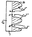
전해 환원의 방법을 제2도로 설명한다. 도면중(6)은 전해 환원하고자 하는 시료이며, (7)은 대향극이다. 이 대향극(7)은 본원에서는 스테인레스판을 사용하지만, 요컨대 불용성의 도전체이면 되므로, 이외에도 백금, 동, 탄소, 납, 은 등을 적용할 수 있다. (8)은 전해액이지만, pH가 6이상일 것이 바람직하다. 도면중의 화살표는 전자(e)가 흐르는 방향이다. 시료(6)면에서의 반응은The method of electrolytic reduction is explained in FIG. 2. In the figure, 6 is a sample to be electrolytically reduced, and 7 is an opposite electrode. Although the counter electrode 7 uses a stainless plate in this application, in other words, since it is an insoluble conductor, platinum, copper, carbon, lead, silver, etc. can also be applied. Although (8) is electrolyte solution, it is preferable that pH is six or more. The arrow in the figure shows the direction in which electrons e flow. The reaction on the surface of the
![]()
![]()
및And
![]()
![]()
이다. CuO가 용해해서 Cu2+는 비교적 주위에서 많이 존재한다고 하면, 외부로부터의 전원에 의해, 보급되는 전자의 양에 의해 (2)식의 반응속도가 결정된다.to be. If CuO is dissolved and Cu 2+ is relatively present in the surroundings, the reaction rate of formula (2) is determined by the amount of electrons supplied by the power source from the outside.
[금속표면의 산화][Oxidation of Metal Surfaces]
산화공정에서 반응을 순차 설명하면, Cu가 NaClO2에 의해 산화되어, Cu2+를 생성하고, 알카리성액중에서 OH-와 반응하여 Cu(OH)2를 생성하며, 또 일부의 Cu2+는 PO3- 4와 반응하여 Cu3(PO4)2와 같은 침전물을 생성하는 것이라고 생각된다. 즉, 추정되는 반응은In order to explain the reaction in the oxidation step, Cu is oxidized by NaClO 2 to form Cu 2+ , and reacted with OH − in an alkaline liquid to form Cu (OH) 2 , and a part of Cu 2+ is PO It is thought to react with 3- 4 to produce a precipitate such as Cu 3 (PO 4 ) 2 . In other words, the estimated response is
![]()
![]()
![]()
![]()
![]()
![]()
![]()
![]()
![]()
![]()
![]()
![]()
![]()
![]()
따라서, 전체적으로 (3)및 (9)의 반응이 진행되므로Therefore, the reaction of (3) and (9) proceeds as a whole.
![]()
![]()
과 같은 반응이 아니냐고 생각된다. 이것으로부터도 알 수 있듯이 금속산화물 (Cu(OH )2↓→CuO+H2O)는 동표면(시료 6표면)에 침전한다. Cu(OH)2는 외관상 미분상고체이며 입경이 극미(수100Å)이므로 상당히 미세한 제2의 요철부(5)가 형성되게 된다.I think it is not the same reaction. As can be seen from this, the metal oxide (Cu (OH) 2 ↓ → CuO + H 2 O) precipitates on the copper surface (
[금속의 석출속도와 밀착력의 관계][Relationship between Precipitation Speed and Adhesion of Metal]
이렇게 해서 얻어진 금속산화막은 전기적으로 환원하면 금속동으로서 석출한다. 석출하는 막의 속도가 완만하면 결정핵의 생성밀도가 낮아, 석출하기 쉬운 결합(킹크 또는 스텝)에 선택적으로 석출하며, 결정은 원래의 미세한 요철형을 없애고 큰 결정립으로 성장하며, 그 결과 수지와의 밀착성은 낮아질 가능성이 있다. 그러나 석출속도를 빨리하면, 원래의 미세한 요철형상을 유지하여 순금속으로서 석출하여, 수지와의 밀착력은 높아지며 또한 내염산성이 향상된다.The metal oxide film thus obtained precipitates as metal copper when it is electrically reduced. The slower the deposition rate, the lower the density of crystal nuclei, and selectively precipitate in bonds (kinks or steps) that are easy to precipitate, and crystals are removed from the original fine irregularities and grow into large grains. Adhesion may fall. However, if the deposition rate is increased, the original fine concavo-convex shape is retained to precipitate as a pure metal, thereby increasing adhesion to the resin and improving hydrochloric acid resistance.
[액온, 휘저어 섞기와 금속의 석출과의 관계][Relationship between Liquid Temperature, Stirring and Precipitation of Metals]
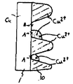
전류밀도를 일정하게 했을 경우는 액온이 낮으면 금속이온(예를 들어 Cu2+)의 확산이 어렵고, 따라서 결정입경이 미세해진다. 한편, 액온이 높으면 금속이온(Cu2+)의 확산이 용이해져, 결정입경이 커진다. 이 모양을 제3도에 나타낸다. 제3a도는 액온이 낮을 경우를, 제3b도는 액온이 높을 경우를 나타낸다. 또, 제3도의 A는 석출되기 쉬운 장소를, B는 석출되기 어려운 장소를 나타낸다. 또한 액을 휘저어 섞는 강도에 의해서도 Cu2+가 움직이기 쉬운 것에 영향을 주어 결정입경의 크기는 달라지게 된다.In the case where the current density is made constant, if the liquid temperature is low, diffusion of metal ions (for example, Cu 2+ ) is difficult, and thus the grain size becomes fine. On the other hand, when the liquid temperature is high, diffusion of metal ions (Cu 2+ ) becomes easy, and the grain size increases. This shape is shown in FIG. FIG. 3A shows the case where the liquid temperature is low, and FIG. 3B shows the case where the liquid temperature is high. In addition, A of FIG. 3 shows the place which is easy to precipitate, and B shows the place which is hard to precipitate. In addition, the stirring strength of the liquid also affects the ease of movement of Cu 2+ , and the grain size is changed.
[전류밀도][Current density]
전해 환원 직후에는 금속은 먼저 본바탕 금속표면의 무수한 결함에서 석출하기 시작한다. 만약 전류밀도가 낮으면 이 원래의 결함을 중심으로 금속이 결정성장하게 된다. 이것은 제3b도의 모양과 비슷하다. 한편, 전류밀도가 높으면 결함 이외, 즉 본바탕의 평면부분(테러스라고도 함)상에도 자다란 금속결정립이 석출하여 이것이 새로운 결함에 해당하므로 결정성장은 작아도 결정성장개소가 많아진다. 이 모양은 제3a도와 비슷하다. 즉 고전류밀도 환원쪽이 미세한 요철을 갖는 금속표면이 얻어지기 쉬우므로, 본원 발명에 있어서는 특히 바람직하다.Immediately after electrolytic reduction, the metal first begins to precipitate from a myriad of defects on the metal surface. If the current density is low, the metal grows around this original defect. This is similar to the shape of Figure 3b. On the other hand, when the current density is high, large metal crystal grains are deposited on the planar portion (also called a truss) of the main base, which is a new defect, so that there are many crystal growth points even if the crystal growth is small. This shape is similar to Figure 3a. That is, since the metal surface which has a fine unevenness | corrugation in a high current density reduction side is easy to be obtained, it is especially preferable in this invention.
[수소환원과의 차이][Difference with hydrogen reduction]
전해 환원과 달리, 수소환원은 고온(650-800℃)조건을 필요로 하기 때문에, 가령 요철면이 있어도 열 때문에 무너져서 평활성이 나와 버린다. 따라서 이 방법에 의한 것은 금속광택이 얻어진다. 금속계면 때문에 내산성은 일단 기대할 수 있으며, 산에 의한 산화막용출에 의한 박리의 불안은 적지만, 밀착성에는 역시 문제가 남는다.Unlike electrolytic reduction, hydrogen reduction requires high temperature (650-800 ° C.) conditions, so that even if there is an uneven surface, it collapses due to heat, resulting in smoothness. Therefore, by this method, metallic luster is obtained. Because of the metal interface, acid resistance can be expected once, and the anxiety of peeling due to oxide film elution by acid is small, but there is also a problem in adhesion.
전해 환원에 있어서는 금속산화물의 각 입자는 즉시 환원되며, 만약 온도가 높아지면 결정성장한다. 또 온도가 낮더라도 반드시 대부분이 확산해서 석출한다. 형상은 외관상 유지하고 있지만, 역시 엄밀하게는 변화하고 있으며, 핵을 중심으로 하여 그 위에 석출해서 결정성장한다. 따라서 상당히 미세한 금속막이 얻어진다.In electrolytic reduction, each particle of the metal oxide is immediately reduced, and crystal growth occurs if the temperature is increased. In addition, even if the temperature is low, most of them will diffuse and precipitate. Although the shape is maintained in appearance, it is also changing strictly, and it is precipitated and crystallized on the nucleus. Thus, a very fine metal film is obtained.
한편, 수소환원은 열처리에 의해 산소가 빠지면 이론상으로는 다공질로 되지만, 이 다공질상태를 유지하는 것이 필요하다. 그러나 500℃이상이 되면 국부는 결정성장이 진행되고, 또 먼저처럼 붕괴가 일어나 국부적으로 다공질상태를 잃어버려 평활화가 진행되는 것이라고 예상된다.On the other hand, hydrogen reduction theoretically becomes porous when oxygen is released by heat treatment, but it is necessary to maintain this porous state. However, when the temperature rises above 500 ° C, it is expected that localization will proceed with crystal growth, and as before, the collapse will occur and the local porous state will be lost and smoothing will proceed.
[본바탕 금속의 형성법][Formation method of the base metal]
일례이지만, 본바탕 금속의 형성법으로서는 스테인레스판상에 금속을 전해로 석출시켜, 이와 같은 판을 2매 준비하여, 이 석출금속면간에 프리프레그를 끼고 가열·가압하면서 석출금속층은 프리프레그와 접착되며, 스테인레스로부터는 용이하게 벗길 수 있다. 물론 이 스테인레스판상의 석출금속을 본바탕 금속으로서 산화 및 전해 환원 순차행하고, 그런 연후에 프리프레그에 접착시켜도 좋다.As an example, as a method of forming the base metal, a metal is deposited on a stainless plate by electrolysis, and two such plates are prepared, and the precipitated metal layer is adhered to the prepreg while being heated and pressurized with a prepreg sandwiched between the surfaces of the deposited metal. It can be peeled off easily from stainless steel. Of course, the precipitated metal on the stainless plate may be subjected to oxidation and electrolytic reduction in sequence as the base metal, and then bonded to the prepreg.
[기타, 총괄][Others, General Affairs]
종래, 금속과 수지를 높은 강도로 접착코자 할 경우, 금속표면을 조화하고, 다시 조화된 금속표면을 산화함으로써 표면상에 산화막을 형성하며, 그 산화막을 통해 금속과 수지를 접착하는 방법이 많이 사용되어 왔다. 그러나 이 방법에 따라 금속-수지복합체를 작성하면, 접착강도에 대해서는 매우 높은 강도의 것이 얻어지지만, 접착계면에 산화막을 사용하기 때문에, 산에 용해하기 쉬워 화학적으로 불안정하다는 결점을 지니고 있다. 이때문에 본원 발명자는 산화막을 사용하지 않고도 산에 대해 안정하고, 또한 수지에 대해 고밀착성을 갖게 하기 위한 처리막에 대해 검토했다. 수지와 금속과의 밀착성을 높은 강도로 하기 위한 산화막의 접착기구에 대해 조사한 결과, 산화막의 표면형상이 복작하게 조화되어 있으며, 이것이 수지와 금속을 강력하게 접착시키기 위한 주인자이고, 또한 금속에 비해 산화막쪽이 수지와의 수소결합을 용이하게 하며, 이 수소결합도 산화막을 통해 금속과 수지를 강력하게 결합시키기 위한 한 인자로서 생각할 수 있다.Conventionally, in order to bond metal and resin with high strength, an oxide film is formed on the surface by harmonizing the metal surface and oxidizing the harmonized metal surface, and a method of bonding metal and resin through the oxide film is often used. Has been. However, when a metal-resin composite is produced according to this method, a very high strength is obtained for the adhesive strength. However, since an oxide film is used for the adhesion interface, the metal-resin composite is easily dissolved in an acid and has a chemical stability. For this reason, the present inventors examined the treatment film for making it stable with respect to an acid and having high adhesiveness with respect to resin, without using an oxide film. As a result of investigating the adhesion mechanism of the oxide film for making the adhesiveness between the resin and the metal high, the surface shape of the oxide film is compounded in a complex manner, which is a master for strongly bonding the resin and the metal, and compared with the metal. The oxide film side facilitates hydrogen bonding with the resin, and this hydrogen bond can also be considered as a factor for strongly bonding the metal and the resin through the oxide film.
그래서, 산화막의 형상에 근접시키고, 또한 수소결합도 생기기 쉽도록 하기 위해 산화막을 전기적으로 환원하여, 산화물을 불가피하게 포함하는 환원막을 금속상에 형성하며, 이 막을 통해 금속과 수지를 접착시키는 방법을 생각해 내기에 이르렀다. 즉, 이 방법을 사용하면산중의 산화물의 양은 종래의 산화막을 구성하고 있는 산화물량에 비해, 훨씬 적다. 이때문에, 내산성이 향상하는 것을 기대할 수 있다. 이것으로부터도 명백한 것처럼 본원 발명을 프린트판의 제조에 적용할 때에는 최소한 관통구멍과 접하는 부분에는 환원금속이 노출하고 있는 것이 바람직하다. 또 접착성에 대해서도 수소결합 및 표면조화에 의한 투묘효과(投描效果)도 기대할 수 있다.Therefore, in order to approximate the shape of the oxide film and to easily generate hydrogen bonds, the oxide film is electrically reduced to form a reducing film containing an oxide inevitably on the metal, and the metal and the resin are adhered through the film. I came to think of it. That is, using this method, the amount of oxide in the acid is much smaller than the amount of oxide constituting the conventional oxide film. For this reason, an acid resistance can be improved. As is apparent from this, when the present invention is applied to the production of a printed plate, it is preferable that at least a portion of the reducing metal is exposed to a portion in contact with the through hole. In addition, the adhesive effect by hydrogen bonding and surface roughening can also be anticipated about adhesiveness.
[전해 환원법]Electrolytic Reduction Method
전해 환원용의 기판으로서, 양면을 동으로 씌원 에폭시~유리크로스판(동박두께; 35㎛, 에폭시~유리크로스층 0.2mm)의 동박상에 화학도금액에 의해 동을 35㎛ 도금하고, 그 후 공기중에서 180℃, 1시간 열처리하며, 다시 화학적인 산화막형성처리한 것을 사용했다. 산화막형성처리조건은 상술한 바와 같다. 기판을 제2도에 나타낸 바와 같은 전해조(10)중에 세트하고, 정전류법에 의해 동박상의 산화막을 전해 환원했다. 전해 환원조건은 액온, 휘저어 섞기, 전류밀도를 바꾸었다. 그리고 전해조(10)에는 온도콘트로울러(11) 및 Ar 가스가 나오는 전해액교반용배선(9)를 부설했다. 환원반응의 종점은 환원전압~시간 곡선을 구하고, 환원파가 급상승할 때의 전압을 근거로 판정했다.As a substrate for electrolytic reduction, 35 micrometers of copper was plated by the chemical plating liquid on the copper foil of the epoxy-glass cross plate (copper foil thickness; 35 micrometers, epoxy-glass cross layer 0.2mm) which covered both surfaces with copper, and after that Heat treatment was performed at 180 ° C. for 1 hour in air, followed by chemical oxidation film formation. The oxide film forming treatment conditions are as described above. The board | substrate was set in the
[접착특성 및 내염산성의 평가법][Evaluation of Adhesive Properties and Hydrochloric Acid Resistance]
접착특성은 비일강도의 측정에 따랐다. 그 시료는 전해 환원 처리한 기판을 프리프레그에 의해 적층접착한 시료를 사용했다. 프리프레그는 두께 0.05mm를 4매 겹쳐서 사용했다. 또 접착조건은 170℃, 90분, 14Kg/㎠로 했다.Adhesion properties were determined by measurement of specific work strength. The sample used the sample which laminated | stacked and bonded the board | substrate which carried out the electrolytic reduction process with the prepreg. The prepreg was used overlapping four sheets of thickness 0.05mm. Moreover, the bonding conditions were 170 degreeC, 90 minutes, and 14 Kg / cm <2>.
내염산성의 시료는 저속커터에 의해 약 10mm2로 절단하고, 단면을 에메리지 (#1000)에 의해 연마한 다음, (#2000) Al2O3연마재를 사용하여 버프연마하고, 염산수용액(17.5%)중에 실온에서 소정시간 담그고, 측면에서 침투시켜 변색한 거리를 측정하는 방법에 따랐다.The hydrochloric acid resistant sample was cut to about 10 mm 2 by a low speed cutter, the cross section was polished by an emery (# 1000), then buffed using (# 2000) Al 2 O 3 abrasive, and an aqueous hydrochloric acid solution (17.5). It was immersed at room temperature for a predetermined time in%), followed by penetrating from the side to measure the discolored distance.
[표면형상의 관찰 및 결정구조의 해석][Surface Shape Observation and Analysis of Crystal Structure]
화학동도금막, 산화처리막 및 전해 환원막의 표면형상은 주사형전자현미경 (SEM)에 의해, 또 결정구조는 반사형전자선회석법에 의해 조사했다. 또한 환원동 표면의 조도가 미세한 일로 해서 광산란을 예상하며 표면반사율의 측정을 했다.The surface shape of the chemical copper plating film, the oxidation treatment film and the electrolytic reduction film was examined by scanning electron microscope (SEM), and the crystal structure by the reflection electron beam lime method. In addition, the surface roughness was measured in anticipation of light scattering due to the fine roughness of the reduced copper surface.
[표면반사율의 측정][Measurement of surface reflectivity]
이 측정에는 상술한 바와 같은 동작원리의 아날라이저를 사용하여 직접 반사율을 측정했다. 측정장치는주식회사히다찌세이사꾸쇼제의 607형컬러 아날아이저이다. 이 장치의 광학계통도는 제4도와 같다.In this measurement, direct reflectance was measured using an analyzer of the above-described operating principle. The measuring device is a 607-color color analyzer manufactured by Hitachi Seisakusho Co., Ltd. The optical system diagram of this apparatus is shown in FIG.
광원(12)은 할로겐램프 120W이며, 여기로부터의 백색광은 내경 200mm의 적분구(13)내에서 확산반사하여, 시료(14) 및 참조백판(15)를 조명한다. 시료(14) 및 백판(15)에 의한 반사광은 투과시료실(16)을 투과한 다음, 미러(17)을 구비한 섹터실로 입사하며, 회전미러(18)에 의해 선택되어서, 교대로 분광기입사슬릿(19)을 조명하는 분광기에 입사한 빛은 회절격자상에 시료상을 결상한 다음, 분산되어서 출사슬릿 (20)을 조명하며, 파장폭 5nm의 단색광만이 출사슬릿(20) 및 필터(21)를 거쳐, 광전자배증관에 입사한다. 그리고, (22)는 입사렌즈, (23)은 섹터모우터, (24)는 그레이팅, (25)는 삼각미러, (26)은 라이트디퓨우저, (27)은 포토마루이다.The
[전해 환원막의 접착특성][Adhesion Characteristics of Electrolytic Reducing Film]
산화막중의 동이온이 환원석출하는 반응으로서는 동이온이 수화한 다음 액중에 해난(解難)하고, 그 후 환원석출하는 경로를 생각할 수 있다. 환원막의 접착특성을 높이기 위해서는 산화막의 표면형상을 환원한 후에도 그대로 유지할 필요가 있으며, 그러기 위해서는 해난한 동이온이 액중 또는 환원막표면을 확산시키지 않고 그 자리에서 즉시 석출할 필요가 있다. 동이온의 확산을 율속(律速)으로 하기 위해서는 환원조건으로서 전류밀도를 높게 하고, 욕온을 낮게 하며, 또한 액교반을 없게 하는 것이 바람직하다. 또, 그 반대의 경우로서, 전류밀도를 낮게 하고, 욕온을 높여 액교반을 있게 하는 조건하에서 환원했을 경우에는 결정핵으로의 석출이온의 보급이 용이해지기 때문에, 결정이 크게 성장하며, 원래의 산화막의 표면형상과는 달리, 환원막이 평활성을 띠기 쉽게 된다.As a reaction in which the copper ions in the oxide film are reduced precipitated, a route in which copper ions are hydrated and then dissolved in the liquid and then reduced precipitated can be considered. In order to improve the adhesion characteristics of the reducing film, it is necessary to maintain the surface shape of the oxide film even after it is reduced, and to do so, it is necessary to dissolve the copper ions immediately on the spot without diffusing the liquid or the surface of the reducing film. In order to make copper ions diffuse at a rate, it is preferable to increase the current density, reduce the bath temperature, and eliminate liquid stirring as the reducing conditions. On the contrary, when the reduction is made under a condition of lowering the current density and increasing the bath temperature to allow the liquid to be stirred, crystals grow large because the precipitation ions are easily spread to the crystal nuclei. Unlike the surface shape of the oxide film, the reducing film tends to be smooth.
그래서, 전해 환원막의 표면형상과 접착강도와의 관계에 대해 조사하기 위해, 25℃, 교반 없음, 및 50℃, 교반 있음의 두 조건을 선정하여 검토했다. 그 결과를 제5도에 나타낸다. 전해 환원 직후의 환원막의 접착특성을 ⅰ및 ⅱ에 나타낸다. 액교반 없음(곡선ⅰ)에서 전류밀도를 낮게 하면 피일강도가 높고, 한편 액교반 있음(곡선ⅱ)에서 전류밀도를 낮게 하고 액온을 높였더니 피일강도가 낮아졌다.Therefore, in order to investigate the relationship between the surface shape of the electrolytic reduction film and the adhesive strength, two conditions of 25 ° C, no agitation, 50 ° C, and agitation were selected and examined. The results are shown in FIG. The adhesion characteristics of the reduced film immediately after electrolytic reduction are shown in X and ii. The lower the current density in the absence of liquid stirring (curve ⅰ), the higher the peel strength, while the lower the current density and the higher the liquid temperature in the liquid stirring (curve ii), the lower the peel strength.
[전해 환원막의 내염산성][HCl Resistance of Electrolytic Reducing Membrane]
전해 환원막의 내염산성(17.5% HCl)에 대해 조사하기 위해, 염산침투거리와 담그는 시간과의 관계를 구했다. 그 결과를 제6도에 나타낸다. 전해 환원조건은 25℃, 교반없음, 0.025, 0.062 5, 0.125, 1.25㎃/㎠ 50℃, 교반있음, 0.025, 0.062 5, 0.125, 1.25㎃/㎠이다. 그리고, 전해 환원의 조건에 따라서는 염산이 침투해도, 침투부가 변색하지 않으며, 침투거리의 판정이 곤란한 점이 있다. 이 때문에, 현미경에 의해 주의 깊게 관찰하기로 했다. 제6도에는 비교를 위해 전해 환원하지 않는 산화처리한 그대로의 시료의 내염산성에 대해 조사한 결과도 병기했다. 산화처리했을 경우(곡선 ⅲ)에는 1시간으로 이미 200㎛정도의 염산침투를 볼 수 있으며, 담그는 시간의 증가와 함께 염산침투량은 단조롭게 증가한다. 이것에 대해, 전해 환원했을 경우, (곡선 ⅳ)은 어떤 조건으로 작성한 막도 염산침투는 6시간 경과해도 발생하지 않는다. 그리고 제6도에는 15시간 담근 후의 결과도 병기했지만, 이 결과로부터 전해 환원이 불충분한 (0.025㎃/㎠)계에서는 약간 염산침투가 발생했지만, 이 이외의 전해 환원한 시료에는 염산의 침투는 없었다. 여하튼간에 전해 환원막은 단지 산화막을 형성한 것에 비해 대폭 내염산성을 향상시킬 수 있다는 것이 명백하다.In order to investigate the hydrochloric acid resistance (17.5% HCl) of the electrolytic reduction membrane, the relationship between the hydrochloric acid penetration distance and soaking time was obtained. The results are shown in FIG. Electrolytic reduction conditions are 25 degreeC, no stirring, 0.025, 0.062 5, 0.125, 1.25 kPa / cm <2> 50 degreeC, with stirring, 0.025, 0.062 5, 0.125, 1.25 kPa / cm <2>. In addition, depending on the conditions of electrolytic reduction, even if hydrochloric acid penetrates, the penetrating portion does not discolor, and it is difficult to determine the penetration distance. For this reason, it was decided to observe carefully with a microscope. In FIG. 6, the hydrochloric acid resistance of the sample subjected to oxidation treatment without electrolytic reduction was also included for comparison. In the case of oxidation treatment (curve), hydrochloric acid penetration of about 200 μm can be seen in 1 hour, and the hydrochloric acid penetration increases monotonously with the increase of soaking time. On the other hand, when electrolytically reduced, (curve ⅳ) does not occur even if the membrane made under certain conditions passes through hydrochloric acid for 6 hours. In addition, although the result after soaking for 15 hours was also written in FIG. 6, hydrochloric acid permeation occurred slightly in the system with insufficient electrolytic reduction (0.025 kPa / cm <2>), but there was no penetration of hydrochloric acid in the electrolytically reduced sample other than this. . In any case, it is evident that the electrolytic reduction film can greatly improve hydrochloric acid resistance compared to merely forming an oxide film.
액온 25℃, 교반 없음의 조건에서 환원석출시켰을 때의 시료의 외관은 1.25㎃/㎠로 환원시켰을 경우, 환원막의 외관은 흑갈색이다. 0.125㎃/㎠에서 환원시켰을 경우에는 외관은 다색이며, 산화처리만의 시료의 외관에 가깝다. 0.0625㎃/㎠로 환원시켰을 경우에는 외관은 산화전단계의 처리에 의해 얻어지는 처리막의 색조에 가까와진다. 그리고, 전류밀도를 0.025㎃/㎠로 했을 경우, 외관은 흑갈색으로 되지만, 이것은 통전시간이 10시간을 초과해도 환원반응이 종점에 달하지 않고 중단되었기 때문이다. 각각의 환원막에 대해 주사형전자현미경으로 관찰한 결과 전류밀도가 0.25㎃/㎠에서 환원한 시료는 전해 환원전의 산화처리한 시료의 표면형상에 가깝다. 0.125㎃/㎠의 경우에 비해, 미립자가 약간이기는 하지만, 크게 성장한다. 0.062㎃/㎠에서 환원했을 경우에는 외관은 산화전단계의 처리에 의해 얻어지는 처리막의 색조에 가까와진다. 그리고, 전류밀도를 0.025㎃/㎠로 했을 경우, 외관은 흑갈색으로 되지만, 이것은 통전시간이 10시간을 초과해도 환원반응이 종점에 달하지 않고 중단되었기 때문이다. 각각의 환원막에 대해 주사형 전자현미경으로 관찰한 결과 전류밀도가 1.25㎃/㎠에서 환원한 시료는 전해 환원전의 산화처리한 시료의 표면형상에 가깝다. 0.125㎃/㎠의 경우에 비해 미립자가 약간이기는 하지만 크게 성장한다. 0.062 5 ㎃/㎠에서는 산화처리의 전단계의 처리한 다음의 표면형상에 가까와진다. 또한 0.025㎃/㎠에서 환원했을 경우에는 0.062㎃/㎠에서 환원한 경우보다도 0.125㎃/㎠와 1.25㎃/㎠ 사이의 조건으로 얻어지는 환원막의 표면형상에 가깝고, 이것은 상술한 0.025㎃/㎠에서 작성한 시료는 전해 환원을 중단했기 때문이다.The external appearance of the sample when reduced precipitation at a liquid temperature of 25 ° C. and without stirring was 1.25 dl /
액온 50℃, 교반 있음의 조건에서 환원석출시켰을 때의 시료의 외관은 1.25㎃/㎠에서 환원했을 경우, 외관은 흑갈색과 갈색이 범벅으로 분포한 색조를 나타내고 있다. 0.125㎃/㎠에서 환원했을 경우는 외관은 다색으로 된다. 0.0625㎃/㎠에서 환원했을 경우는 적갈색으로 되며, 산화처리의 전반처리로 얻어지는 처리막의 색조에 가깝다. 또한, 0.025㎃/㎠ 에서 환원했을 경우, 더욱 동색에 가까와지는 것이라고 생각되었지만 휘저어 섞지 않은 0.025㎃/㎠에서 환원한 시료와 같이, 전해 환원이 불충분하며, 황적색으로 되었다. 여기서 사용한 시료의 표면형상에 대해 주사형전자현미경에 의해 조사한 결과, 1.25㎃/㎠에서 환원한 시료의 표면형상은 산화처리한 시료의 표면형상과 비슷하다. 0.125㎃/㎠에서는 0.1㎛ 이하의 자다란 환원동의 결정립을 볼 수 있지만, 1.25㎃/㎠에서 환원했을 경우에 비해 결정립의 수가 적고, 평활성을 띠게 된다. 0.062 5㎃/㎠에서 환원한 시료는 환원동의 결정립이 크게 성정하며, 0.1~0.5㎛의 결정립에 섞여, 1㎛ 정도의 큰 결정립도 볼 수 있다. 0.025㎃/㎠에서 환원한 시료는 표면형상이 0.062 5㎃/㎠에서 환원처리해서 얻어지는 막의 경우와 대충 같은 정도이다. 그리고, 표면이 미세한 결정으로 덮여 있는 시료는 피일강도가 높은 값을 나타내며, 접착특성이 환원막의 표면형상에 강하게 의존하고 있는 것을 볼 수 있다.The external appearance of the sample when reduced precipitation was carried out under the condition of a liquid temperature of 50 ° C. and stirring showed a color tone in which black brown and brown were distributed in a bumpy manner. When reduced at 0.125 Pa /
다음에 액온 25℃, 교반없음의 조건에서, 각 전류밀도에 있어서 얻어진 환원막의 반사형전자선회절상과 액온 50℃, 교반있음의 경우에 대해 마찬가지로 관찰한 결과, 및 화학산화처리막의 반사형전자선회절상을 검토해 보는 회절선의 패터언을 해석하기 위해, 먼저 ASTM 카아드 및 Au의 표준시료를 근거로 Cu, Cu2O, CuO 및 Cu3(PO4)2의 각 회절선의 직경을 구했다. 그 결과, 산화처리막 및 환원막의 어떤 시료에도 Cu 및 Cu2O가 약간이지만 볼 수 있다. 본래, 환원막의 완전금속동화를 노린 것이지만, 그처럼은 되지 않고 불가피하게 남았다. 그리고 이상은 본원발명의 일태양에 지나지 않으며 물론 이들 여러 조건으로는 한정되지 않는다.Next, the reflection electron beam diffraction image of the reduced film obtained at each current density and the liquid temperature of 50 ° C. with agitation under the condition of a liquid temperature of 25 ° C. and agitation were similarly observed. to analyze the L Turn | diffraction line to examine, on the basis of the first reference samples of ASTM car ad Cu and Au, Cu 2 O, CuO and Cu 3 (PO 4) was determined for each diffraction line diameter of 2. As a result, Cu and Cu 2 O are slightly visible in any of the samples of the oxidation treatment film and the reduction film. Originally aimed at fully metal assimilating the reducing film, it was not so and remained inevitable. And the above is only one aspect of this invention, and of course is not limited to these various conditions.
[직접반사율의 측정결과][Measurement Result of Direct Reflectance]
표면반사율은 1.25㎃/㎠, 액온 25℃, 휘저어 섞지 않은 조건하에서 상기 방법에 의한 전해 환원을 행한것을 본원발명의 시료로 했다. 이 시료의 외관은 흑갈색무광택이다. 비교예로서 본 바탕동편(자연상화의 부분 있음, 동색), 비교예 2로서 고온수소환원에 의한 동편(동색, 광택 있음)을 사용한다. 측정결과는 제7도와 같았다. 제7도에 있어서 곡선 ⅳ은 본원발명시료의 직접반사율을, 곡선 V은 역시 확산반사율을 나타낸다. 또 곡선 Vi은 비교예 1의 시료의 직접반사율을, 곡선 Vii은 역시 확산반사율을 나타낸다. 또한 곡선 Viii은 비교예 2의 시료의 직접반사율을, 곡선 ⅤⅰⅤ은 역시 확산반사율을 나타낸다. 그리고, 확산반사율은 제4도의 라이트디퓨우저(22)를 트랩대신 측정했다.The surface reflectance was 1.25 kV /
제7도에서 명백한 것처럼 본원발명시료는 이른바 금속동 표면에 볼 수 있어야 할 높은 직접반사율은 보이지 않는다.As apparent from FIG. 7, the sample of the present invention does not show a high direct reflectance which should be seen on the surface of the metal copper.
다음에 본원발명의 더욱 구체적인 응용예를 기술한다.Next, more specific application examples of the present invention will be described.
[실시예 1]Example 1
본원발명의 일실시예를 제8도에 의거하여 다음에 설명한다. 유리섬유 강화에폭시수지판(28)의 양면에 동박(29)을 열압착한 것(제8a도)의 표면을 다음에 나타낸 바와 같은 조성An embodiment of the present invention will be described next with reference to FIG. The composition of the surface of the
NaOH 5g/ℓNaOH 5g / ℓ
Na3PO4·2H2O 10g/ℓNa 3 PO 4 2H 2 O 10 g / ℓ
NaClO230g/ℓNaClO 2 30g / ℓ
을 갖는 인산계의 수용액에 의해 처리하여 동박(29) 표면에 동산화막(30)을 형성했다(제8b도). 이어서 수세후, 후기 레지스트와의 밀착성을 해치지 않을 정도로 동산화막(30)을 전해 환원하고, 전해 환원금속층(2)을 얻었다(제8c도).The
이 전해 환원은 전해 환원용의 액으로서 NaOH에 의해 pH 120으로 조정한 액을 사용하여, 액온을 25℃로 하고, 환원전류밀도를 1.25㎃/㎠로 하며, 대극에는 스테인레스판을 사용하여, 상기 동의 표면상에 형성한 산화막을 환원처리했다.This electrolytic reduction was carried out using a liquid adjusted to pH 120 with NaOH as the liquid for electrolytic reduction, the liquid temperature of 25 ° C., the reduction current density of 1.25 mA /
다음에, 이 환원처리막에 부착한 전해액을 수세한 다음, 충분히 건조하여, 그 위에 드라이필름(31)에 의해 레지스트패터언을 형성하고(제8d도), 다음에 이하에 나타낸 바와 같은 성분Next, the electrolyte solution adhered to the reduction treatment film is washed with water, then sufficiently dried to form a resist pattern on the
CuSO4·5H2O 7gCuSO 4 5H 2 O 7g
에틸렌디아민 4초산 30g30 g of ethylenediamine tetraacetic acid
37% HCHO 3ml37% HCHO 3ml
NaOH pH가 12.5로 되도록 첨가Add NaOH pH to 12.5
폴리에틸렌글리코올 20mlPolyethylene Glycool 20ml
(평균분자량 450) 30mg(Average molecular weight 450) 30 mg
2,2' 디필리딜 30mg2,2 'Dipiridyl 30mg
을 1ℓ의 물에 용해해서 얻어지는 농도로 조정한 도금액을 사용하여 회로부상에 동(32)을 회로도체로서 필요한 두께로 화학도금했다(제8e도). 그 결과 화학도금액의 침투에 의거한 비회로부에의 동의 석출은 없었다.The
다음에 드라이필름(31)의 레지스트패터언을 제거하고(제8f도), 그 후, 다음에 나타낸 바와 같은 조성Next, the resist pattern of the
FeCl3400g/ℓFeCl 3 400g / ℓ
Conc·HCl 20㎖/ℓConcHCl 20ml / l
을 갖는 에칭액에 의해, 비회로부의 동박(29)을 에칭제거하여 유리섬유 강화에폭시수지기판(28)상에 동(32)을 남기고 동배선을 완성했다(G).The
얻어진 동배선의 패터언은 동도체폭(㎛)/도체간격(㎛)이 49/51이며, 이것은 사용한 레지스트패터언형상의 이것에 대응하는 비 50/50에 가깝고 양호한 소망의 패터언정도를 갖는 것을 알았다.The obtained copper wiring pattern has a conductor width (µm) / conductor spacing (µm) of 49/51, which is close to the
[실시예 2]Example 2
실시예 1에 있어서의 유리섬유강화에폭시수지판(28) 대신 폴리이미드판을 사용한 이외는 실시예 1과 같은 방법, 조건에 의해 실시했다. 그 결과, 얻어진 동배선의 패터언의 상기 비는 49/51이며, 이것은 사용한 레지스트패터언형상의 그것에 대응하는 비 50/50에 가깝고, 양호한 패터언정도를 갖는 것을 알았다.It carried out by the method and conditions similar to Example 1 except having used the polyimide board instead of the glass fiber reinforced
[실시예 3]Example 3
실시예 1에 있어서 드라이필름의 레지스트 대신 액상의 레지스트를 사용하며 또한 전해액의 pH를 6.0으로 하고, 그 이외는 실시예 1과 같은 방법에 의해 실시했다. 그 결과 얻어진 동배선의 패터언의 상기 비는 48/52이며, 이것은 사용한 레지스트패터언형상의 이것에 대응하는 비 50/50에 가깝고, 양호한 패터언정도를 갖는 것을 알았다.In Example 1, a liquid resist was used instead of the resist of a dry film, pH of electrolyte solution was 6.0, and it carried out by the method similar to Example 1 except others. As a result, the said ratio of the pattern wiring of the copper wiring obtained was 48/52, and it turned out that it is close to the
[실시예 4]Example 4
실시예 1에 있어서 동박 표면의 산화처리용의 액으로서, 인산계의 수용액 대신In Example 1, a solution for oxidation treatment on the surface of copper foil, instead of an aqueous solution of phosphoric acid
KMnO410g/ℓKMnO 4 10 g / ℓ
NaOH 10g/ℓNaOH 10g / ℓ
이라는 조성을 갖는 수용액을 사용하여 동박 표면을 처리한 이외는 실시예 1과 같은 방법, 조건에 의해 실시했다. 그 결과, 얻어진 동배선의 패터언의 상기 비는 49/51이며, 이것은 사용한 레지스트패터언형상의 이것에 대응하는 비 50/50에 가깝고, 양호한 패터언정도를 갖는 것을 알았다.It carried out by the method and conditions similar to Example 1 except having processed the copper foil surface using the aqueous solution which has the composition of this. As a result, it was found that the above ratio of the obtained patterned copper wiring was 49/51, which was close to the
전해 환원시에 있어서의 동산화막의 전해 환원반응은 다음과 같다. 즉 주반응으로서 다음의 반응기구를 생각할 수 있다.The electrolytic reduction reaction of the copper oxide film at the time of electrolytic reduction is as follows. That is, the following reactor mechanism can be considered as the main reaction.
![]()
![]()

전해 환원액의 pH로서는 pH 6이상이 바람직하다. 그 이유는 pH가 약 5.5 이하에서는As pH of an electrolytic reduction liquid,
![]()
![]()
와 같은 반응이 조속히 진행하며, 동박상에 산화막을 형성한 기판을 전해액에 담그었을 경우, 소망의 형상의 전해 환원막이 얻어지기 어렵기 때문이다.This is because the reaction as described above proceeds quickly and the electrolytic reduction film having a desired shape is hardly obtained when the substrate having the oxide film formed on the copper foil is immersed in the electrolyte solution.
그리고, 이상의 각 실시예의 의해 얻어진 동배선판은 전해 환원된 다음의 막중에, 그 형성시에 사용한 상기 산화처리용액에 응해 인, 망간 또는 염소나 산소를 포함하고 있는 것이 발견되었다.And it was found that the copper wiring board obtained by each of the above examples contained phosphorus, manganese, chlorine, or oxygen in response to the oxidation treatment solution used at the time of formation in the following electrolytically reduced film.
상기 각 실시예는 절연성기판(28)의 양면에 회로를 형성하는 것으로서 설명했지만, 한쪽면에만 회로를 형성할 경우에도 본원발명은 적용가능한 것은 물론이다. 또 기판(28)은 동박(29)을 열압착한 것으로서 설명했지만 이 대신 화학도금에 의해 동의 박층을 표면에 실시한 절연기판을 사용할 수도 있다.Although each of the above embodiments has been described as forming circuits on both sides of the insulating
[비교예 3]Comparative Example 3
비교를 위해, 실시예 1의 전해 환원의 프로세스(C)를 하지 않은 이외는 실시예 1과 같은 조건으로 선행예의 프로세스에 의해, 유리섬유이며시수지판상에 동배선을 형성했더니, 화학도금시에 동박상에 형성한 산화막중의 동이온의 일부가 환원되며, 이후 계속해서 비회로부상에 도금액중의 동이온이 환원석출하게끔 되었다. 그 결과, 동배선의 패터언의 상기 비는 43/57이며, 이것은 사용한 레지스트패터언형상의 이것에 대응하는 비 50/50와는 크게 상이하며, 패터언정도가 불량했었다.For comparison, except that the electrolytic reduction process (C) of Example 1 was not performed, copper wiring was formed on the glass resin and the resin plate by the process of the preceding example under the same conditions as in Example 1, and at the time of chemical plating Part of the copper ions in the oxide film formed on the copper foil was reduced, and subsequently, the copper ions in the plating liquid were reduced and precipitated on the non-circuit portion. As a result, the said ratio of the pattern wiring | wire of copper wiring is 43/57, and this differs significantly from the
[실시예 5]Example 5
본원발명의 일실시예를 제9도에 의거하여 설명한다. 양면에 동박(29)을 열압착한 유리섬유강화에폭시수지판(28)의 동박(29)상에 동(32)을 화학도금에 의해 회로도체로서 필요한 두께로 부착시킨 다음, 동(32)의 표면을 다음에 나타낸 바와같은 조성An embodiment of the present invention will be described with reference to FIG. The
NaOH 5g/ℓNaOH 5g / ℓ
Na3PO4·2H2O 10g/ℓNa 3 PO 4 2H 2 O 10 g / ℓ
NaClO230g/ℓNaClO 2 30g / ℓ
을 갖는 인산계의 수용액으로 처리하여, 동(32)의 표면에 동산화막(30)을 형성하고 (제9a도), 수세후, 동산화막(30)을 후술하는 프리프레그와의 밀착성을 손상시키지 않을 정도로 전해 환원했다(제9b도). 전해 환원은 NaOH 5g/ℓ 수용액(pH 12)을 사용하여, 2㎃/㎠로 실시했다. 대극에는 스테인레스판을 사용했다.Treating with a phosphoric acid-based aqueous solution to form a
다음에, 상기 전해 환원금속층(2)상에 드라이필름(31)에 의해 레지스트패터언을 형성하고(제9c도), 이어서 염화제2철계의 수용액Next, a resist pattern is formed on the electrolytic
FeCl3400g/ℓFeCl 3 400g / ℓ
Conc·HCl 20㎖/ℓConcHCl 20ml / l
에 의해 비회로부의 동(29 및 32)을 에칭제거하고(제9c도), 다음에 드라이필름(31)을 부착한 채의 상태에서, 다시 상기와 같은 인산계의 수용액을 사용하여 동배선의 측면에 동산화막(33)을 형성하고(제9e도), 다음에 드라이필름(31)을 예를 들어 염화메틸렌등에 의해 제거했다(제9f도).The
이와 같이해서 동배선이 이루어진 단판을 유리섬유로 강화된 에폭시수지계의 프리프레그(34)를 개재시켜서 겹쳐 쌓아, 호트프레스를 사용하여 가열·가압접착하여 (단, 최외층의 단판으로서는 최외면측에 동배선이 이루어져 있지 않는 동박 29 그대로의 것을 사용함), 소정의 회로도체 부분을 관통하는 관통공 H를 뚫었다(제9g도). 이 상태에 있어서는 동배선(32)의 측면에 형성된 동산화막(33)은 관통공 내면에 노출하지 않으며, 그 곳에서 격리된 위치에 있다. 그 후, 관통공 내면에 화학도금을 위한 촉매를 부여하고, 다음에 화학도금에 의해 관통공 내면 및 최외층 전면에 동(32)을 회로도체로서 필요한 두께로 도금하고, 이어서 드라이필름에 의해 최외층에 레지스트패터언을 형성한 다음 에칭에 의해 비회로부의 동을 제거하고, 그 후, 드라이필름을 제거하여 다층배선판을 완성했다(제9h도).In this way, the single plates made of copper wiring are stacked by interposing
이와 같이해서 완성된 다층배선판의 구조는 제9h에 나타낸 바와 같이, 동도체의 평면부는 동의 산화물로 피복되어 있지 않으며 그 측면부만이 동의 산화물로 피복되어 있는 것으로 되어 있다.In the structure of the multilayer wiring board thus completed, as shown in 9h, the planar portion of the copper conductor is not covered with copper oxide, and only the side portion thereof is covered with copper oxide.
상기 프로세스에 있어서는 다층배선판은 관통공 및 최외층에의 화학도금전처리공정시, 관공내에 있어서 산성액에 동산화막층이 직접 닿는 일은 없다. 이 때문에 상기 프로세스에 따라 작성한 다층배선판은 내염산성에 뛰어나며, 또한 프리프레그와 동배선이 고밀착성을 가지며, 나아가서는 배선밀도도 높은 것으로 할 수 있었다. 실측에 의하면 내염산강도는 전해 환원하지 않는 시료에 비해 48배로 되며, 피일강도는 1.1Kg/cm였다.In the above process, the multilayer wiring board does not directly contact the copper oxide film layer with the acidic liquid in the through-hole during the chemical plating pretreatment process to the through-hole and the outermost layer. For this reason, the multilayer wiring board produced by the said process was excellent in hydrochloric acid resistance, and the prepreg and copper wiring had high adhesiveness, and also the wiring density was high. According to the measurement, the hydrochloric acid strength was 48 times higher than that of the sample which was not electrolytically reduced, and the skin strength was 1.1 Kg / cm.
[실시예 6]Example 6
실시예 5에 있어서의 기판 및 프리프레그용 유기수지로서 에폭시 대신 폴리이미드를 사용하며, 또한 전해액의 pH를 6.0으로 하고, 그 이외는 실시예 5와 같은 방법에 의해 실시했다. 그 결과, 전해 환원하지 않는 시료에 비해, 내염산성이 50배이며, 또 유기수지에 대한 동배선의 피일강도는 1.2Kg/cm이고, 어떤 점도 뛰어난 특성을 나타내는 고밀도 배선패터언을 갖는 다층배선판이 얻어졌다.As the substrate and the prepreg organic resin in Example 5, polyimide was used instead of epoxy, and the pH of the electrolytic solution was 6.0, and the same procedure as in Example 5 was carried out. As a result, the multilayer wiring board having a high-density wiring pattern which exhibits properties of 50 times hydrochloric acid resistance and copper wire strength to the organic resin and 1.2Kg / cm and excellent viscosity in comparison with the sample which is not electrolytically reduced. Obtained.
[실시예 7]Example 7
실시예 5에 있어서, 드라이필름 대신 액상의 레지스트를 사용하며, 또한 전해액의 pH를 6.0으로 하고, 그 이외는 실시예 5와 같은 방법에 의해 실시했다. 그 결과, 내염산성 및 밀착성에 뛰어난 고밀도배선패터언을 갖는 다층배선판이 얻어졌다. 내염산성은 45배, 피일강도는 1.2Kg/cm였다.In Example 5, liquid resist was used instead of dry film, and pH of electrolyte solution was 6.0, and it carried out by the method similar to Example 5 except others. As a result, a multilayer wiring board having a high density wiring pattern excellent in hydrochloric acid resistance and adhesiveness was obtained. Hydrochloric acid resistance was 45 times and skin strength was 1.2Kg / cm.
[실시예 8]Example 8
실시예 5에 있어서의 동박(29) 표면의 산화처리용의 액으로서 인산계의 수용액 대신As a liquid for oxidation treatment on the surface of
KMnO410g/ℓKMnO 4 10 g / ℓ
NaOH 10g/ℓNaOH 10g / ℓ
라는 조성의 수용액을 사용하여 동박 표면을 처리한 것 이외는 실시예 5와 같은 방법, 조건에 의해 실시했다. 그 결과, 내염산성 및 밀착성에 뛰어난 고밀도배선패터언을 갖는 다층배선판이 얻어졌다. 내염산성은 47배, 피일강도는 1.1Kg/cm였다.It carried out by the method and conditions similar to Example 5 except having processed the copper foil surface using the aqueous solution of the composition. As a result, a multilayer wiring board having a high density wiring pattern excellent in hydrochloric acid resistance and adhesiveness was obtained. Hydrochloric acid resistance was 47 times and skin strength was 1.1Kg / cm.
그리고, 상기에 있어서 내염산성 및 피일강도는 다음의 평가법으로 평가한 것이다.In addition, hydrochloric acid resistance and skin strength are evaluated by the following evaluation method in the above.
내염산성 :Hydrochloric acid resistance:
각각의 샘플을(1+1) 염산수용액중에 1시간 담그고, 염산중에 동산화막이 용해한 폭을 비교하여, 폭이 넓을수록 불량한 것으로 했다.Each sample was immersed in (1 + 1) hydrochloric acid aqueous solution for 1 hour, and the width | variety which the copper oxide film melt | dissolved in hydrochloric acid was compared, and the width was made into worse.
피일강도 :Filing strength:
일반적으로 사용되고 있는 주지의 평가법을 사용했다. 즉 동막의 폭이 10mm로 되도록 에칭하고, 동막의 일부를 벗겨, 벗긴 부분 및 기판의 수지부를 각기 인장시험기의 지그(Jig)에 고정시켜, 10cm/분의 속도로 수지판에서 동막을 수직방향으로 벗기고, 막이 벗겨질 때의 응력 P(Kg)를 단위폭(cm)당으로 나타낸 것(PKg/cm)으로 표시했다.Commonly used well-known evaluation methods were used. That is, the copper film was etched to have a width of 10 mm, a part of the copper film was peeled off, and the peeled portion and the resin part of the substrate were fixed to the jig of the tensile tester, respectively, and the copper film was vertically oriented on the resin plate at a speed of 10 cm / min. It peeled off and expressed the stress P (Kg) at the time of peeling a film | membrane as what was shown per unit width (cm) (PKg / cm).
이상의 각 실시예에 있어서의 제9a도의 공정에 있어서, 회로로 되어야 할 동층 (32)은 화학도금 대신 전기도금에 의해 동박(29)에 붙여도 좋다. 또 동박(29)을 열압착한 절연기판(28)을 사용하는 것으로서 설명했지만, 동박(29) 대신 동의 박층을 화학도금에 의해 표면에 실시한 절연기판을 사용해도 좋다.In the process of FIG. 9A in each of the above embodiments, the
또 이상의 각 실시예에서는 적층되어야 할 각 단판에는 그 양면에 회로를 형성하는 것으로서 설명했지만 소망에 따라, 모든 또는 일부의 단판에는 한쪽면에만 회로를 형성해도 된다.In each of the embodiments described above, circuits are formed on both surfaces of each end plate to be stacked, but if desired, circuits may be formed on only one side of all or part of the end plates.
그리고, 회로설계의 필요에 따라서는 최외면에는 동배선을 형성하지 않아도 된다.And, depending on the needs of the circuit design, it is not necessary to form the copper wiring on the outermost surface.
[실시예 8]Example 8
양면에 동을 바른 유리에폭시수지판(28)상에 동(32)을 화학도금에 의해 두껍게 붙인 다음, 동(32)의 표면을 다음에 나타낸 바와 같은 벤조트리아졸 및 인산계수용액에 의해 동 표면에 산화막 및 금속보호막을 형성하고, 수세후, 산화막을 전해 환원한다.The
벤조트리아졸 100ppmBenzotriazole 100ppm
NaOH 5g/ℓNaOH 5g / ℓ
Na3PO4·2H2O 10g/ℓNa 3 PO 4 2H 2 O 10 g / ℓ
NaClO230g/ℓNaClO 2 30g / ℓ
다음에 드라이필름(31)에 의해 레지스트패터언을 형성하고, 이어서 염화제2철계의 수용액Next, a resist pattern is formed by the
FeCl3350g/ℓFeCl 3 350g / ℓ
Cone, HCl 20㎖/ℓCone, HCl 20ml / ℓ
에 의해, 비회로부의 동을 에칭제거하고, 다음에 드라이필름(31)을 입힌 채의 상태에서, 다시 인산계의 수용액을 사용하여 동배선의 측면에 산화막을 형성하며, 다음에 드라이필름을 박리한다. 다음에 양측을 동으로 입힌 판의 한쪽은 동박인 채의 상태로 하고, 즉 한쪽면은 드라이필름에 의해 전면마스크하고, 다음에 나머지 한쪽면은 화학도금한 다음, 제9b~f도의 공정에 따라 처리한 기판을 작성한다. 전해 환원조건은 NaOH 5g/ℓ수용액을 사용하여, 0.2mA/d㎡에서 실시했다.By etching, the copper of the non-circuit part is etched away, and then, while the
[실시예 9]Example 9
실시예 8에 있어서, 기판 및 프리프레그용의 유기수지로서 에폭시수지 대신 폴리이미드수지를 사용하며, 그 이외는 실시예 8과 같은 방법에 의해 실시했다. 그 결과, 내염산성 및 밀착성이 뛰어난 고밀도 배선패터언을 갖는 다층배선판이 얻어졌다.In Example 8, polyimide resin was used instead of epoxy resin as the organic resin for the substrate and the prepreg, and the same procedure was followed as in Example 8. As a result, a multilayer wiring board having a high-density wiring pattern excellent in hydrochloric acid resistance and adhesion was obtained.
[실시예 10]Example 10
실시예 8에 있어서, 최외층에는 한쪽면을 동으로 바른 판을 사용했다. 그 이외는 실시예 8과 같은 방법에 의해 실시했다. 그 결과, 내염산성 및 밀착성에 뛰어난 고밀도 배선패터언을 갖는 다층배선판이 얻어졌다.In Example 8, a plate coated with copper on one side was used for the outermost layer. Other than that was carried out by the same method as in Example 8. As a result, a multilayer wiring board having a high density wiring pattern excellent in hydrochloric acid resistance and adhesiveness was obtained.
[실시예 11]Example 11
실시예 8에 있어서, 드라이필름 대신, 액상레지스트를 사용하며, 그 이외는 실시예 8과 같은 방법에 의해 실시했다. 그 결과, 내염산성 및 밀착성에 뛰어난 고밀도 배선패터언을 갖는 다층배선판이 얻어졌다.In Example 8, a liquid resist was used in place of the dry film, and the same procedure was followed as in Example 8. As a result, a multilayer wiring board having a high density wiring pattern excellent in hydrochloric acid resistance and adhesiveness was obtained.
[실시예 12]Example 12
실시예 8에 있어서, 동박 표면의 산화처리용의 액으로서 인산계액 대신In Example 8, instead of the phosphoric acid-based liquid as the liquid for oxidation treatment on the surface of the copper foil
KMnO415g/ℓKMnO 4 15 g / ℓ
NaOH 15g/ℓNaOH 15g / ℓ
을 사용하여, 동박 표면을 처리했다. 그 이외는 실시예 8과 같은 방법에 의해 실시했다. 그 결과, 내염산성 및 밀착성에 뛰어난 고밀도 배선패터언을 갖는 다층배선판이 얻어졌다.Using, the copper foil surface was processed. Other than that was carried out by the same method as in Example 8. As a result, a multilayer wiring board having a high density wiring pattern excellent in hydrochloric acid resistance and adhesiveness was obtained.
[실시예 13]Example 13
실시예 8에 있어서, 인산계의 수용액에 벤조트리아졸 1,000ppm을 첨가하여 동 표면에 산화막을 형성했다. 그 이외는 실시예 8과 같은 방법에 의해 실시했다. 그 결과, 내염산성 및 밀착성에 뛰어난 고밀도 배선패터언을 갖는 다층배선판이 얻어졌다.In Example 8, 1,000 ppm of benzotriazole was added to the aqueous solution of phosphoric acid system, and the oxide film was formed on the copper surface. Other than that was carried out by the same method as in Example 8. As a result, a multilayer wiring board having a high density wiring pattern excellent in hydrochloric acid resistance and adhesiveness was obtained.
[실시예 14]Example 14
실시예 8에 있어서, 인산계의 수용액에 벤조트리아졸 대신 티오디에틸렌 글리코올을 100ppm 첨가한 이외는 실시예 8과 같은 방법에 의해 실시했다. 그 결과, 내염산성 및 밀착성이 모두 특성이 양호했었다.In Example 8, it carried out by the method similar to Example 8 except having added 100 ppm of thiodiethylene glycool instead of benzotriazole to the phosphoric acid aqueous solution. As a result, both hydrochloric acid resistance and adhesiveness had favorable characteristics.
[실시예 15]Example 15
양면을 동으로 바른 유리에폭시 수지판에 동(32)을 화학도금에 의해 두껍게 붙인 다음, 동 표면을 다음에 나타낸 바와같은 인산계의 수용액
NaOH 5g/ℓNaOH 5g / ℓ
Na3PO4·2H2O 10g/ℓNa 3 PO 4 2H 2 O 10 g / ℓ
NaClO230g/ℓNaClO 2 30g / ℓ
에 의해, 동 표면에 산화막을 형성하고, 수세후, 산화막을 전해 환원하다. 전해 환원 조건은 NaOH 5g/ℓ 수용액을 사용하여, 전류밀도 0.2mA/dm2로 행한다. 다음에 환원막 표면에 다음에 나타낸 바와 같은 인산계의 수용액By this, an oxide film is formed on the copper surface, and after washing with water, the oxide film is electrolytically reduced. The electrolytic reduction conditions are performed at a current density of 0.2 mA / dm 2 using NaOH 5 g / L aqueous solution. Next, an aqueous solution of phosphoric acid based on the surface of the reduction film as shown below.
NaOH 0.5g/ℓNaOH 0.5g / ℓ
Na3PO41.0g/ℓNa 3 PO 4 1.0 g / ℓ
NaClO23.0g/ℓNaClO 2 3.0g / ℓ
에 의해, 산화막층을 현성한다. 그때의 막두께를 100Å로 했다.By this, an oxide film layer is formed. The film thickness at that time was 100 kPa.
다음에 드라이필름(31)에 의해 레지스트패터언을 형성하고, 이어서 염화제2철계의 수용액Next, a resist pattern is formed by the
FeCl340g/ℓFeCl 3 40g / ℓ
Cone, HCl 20㎖/ℓCone, HCl 20ml / ℓ
에 의해 비회로부의동(32)을 에칭제거하고, 다음에 드라이필름(31)을 붙인 채의 상태에서, 다시 인산계의 수용액을 사용하여 동배선의 측면에 산화막을 형성하며, 다음에 드라이필름을 박리한다. 그런 연후에 이것을 프리프레그와 함께 호트프레스에 의해 가온가압해서 프리프레그를 경화시킨다. 그리고 양측 동으로 바른 판의 한쪽은 동박의 상태로 하고, 즉 한쪽면은 드라이필름에 의해 전면마스크로 하고, 다음에 나머지 한쪽면은 화학도금한 다음, 제9b~f도의 공정에 따라 처리한 기판을 작성한다.The
[실시예 16]Example 16
실시예 15에 있어서, 기판 및 프리프레그용의 유기수지로서 에폭시수지 대신 폴리이미드수지를 사용하며, 그 이외는 실시예 15와 같은 방법에 의해 실시했다. 그 결과 내염산성 및 밀착성이 뛰어난 고밀도배선패터언을 갖는 다층배선판이 얻어졌다.In Example 15, polyimide resin was used instead of the epoxy resin as the organic resin for the substrate and the prepreg, and the same procedure was followed as in Example 15. As a result, a multilayer wiring board having a high density wiring pattern excellent in hydrochloric acid resistance and adhesion was obtained.
[실시예 17]Example 17
실시예 15에 있어서, 최외층에는 한쪽면을 동으로 바른 판을 사용했다. 그 이외는 실시예 15와 같은 방법에 의해 실시했다. 그 결과, 내염산성 및 밀착성이 뛰어난 고밀도 배선패터언을 갖는 다층배선판이 얻어졌다.In Example 15, a plate coated with copper on one side was used for the outermost layer. Others were carried out by the same method as in Example 15. As a result, a multilayer wiring board having a high-density wiring pattern excellent in hydrochloric acid resistance and adhesion was obtained.
[실시예 18]Example 18
실시예 15에 있어서, 드라이필름 대신, 액상레지스트를 사용하며, 그 이외는 실시예 15와 같은 방법에 의해 실시했다. 그 결과, 내염산성 및 밀착성이 뛰어난 고밀도 배선패터언을 갖는 다층배선판이 얻어졌다.In Example 15, a liquid resist was used instead of a dry film, and the same procedure was followed as in Example 15. As a result, a multilayer wiring board having a high-density wiring pattern excellent in hydrochloric acid resistance and adhesion was obtained.
[실시예 19]Example 19
실시예 15에 있어서, 동박 표면의 산화처리용의 액으로서 인산계의 액 대신In Example 15, the liquid for oxidation treatment of the surface of copper foil instead of the phosphoric acid-based liquid
KMnO415g/ℓKMnO 4 15 g / ℓ
NaOH 15g/ℓNaOH 15g / ℓ
을 사용하여 동박 표면을 처리했다. 그 이외는 실시예 1과 같은 방법에 의해 실시했다. 그 결과, 내염산성 및 밀착성에 뛰어난 고밀도 배선패터언을 갖는 다층배선판이 얻어졌다.The copper foil surface was processed using. Other than that was performed by the method similar to Example 1. As a result, a multilayer wiring board having a high density wiring pattern excellent in hydrochloric acid resistance and adhesiveness was obtained.
[실시예 20]Example 20
금속동박(막두께 50㎛)의 한쪽면을 증류수 1ℓ당One side of metal copper foil (
CuCl240gCuCl 2 40g
HCl(35%) 300ml300 ml HCl (35%)
을 포함하는 액에 의해, 30℃로 50초동안 담그고, 동박 표면을 조화한 다음, 증류수 1ℓ당Soak for 30 seconds at 30 ℃ by the liquid containing, and after adjusting the surface of the copper foil, per 1 liter of distilled water
Na3PO4·12H2O 15gNa 3 PO 4 12H 2 O 15 g
NaClO225gNaClO 2 25g
NaOH 10gNaOH 10g
을 포함하는 액에 의해 70℃에서 120초 담그고, 동박 표면상에 동화합물층을 형성한다. 다음에, 증류수 1ℓ당Immerse 120 seconds at 70 degreeC with the liquid containing these, and form a copper compound layer on the copper foil surface. Next, per liter of distilled water
NaOH 10gNaOH 10g
을 포함하는 액을 사용프리, 액온 25℃에 있어서, 전류밀도 0.5㎃/㎠에서 전기적으로 환원했다. 다음에, 유리크로스로 보강된 폴리이미드계 프리프레그를 사용하여, 동화합물층을 환원처리한 동박을 사용하고, 환원처리면을 프리프레그측을 향해 접착했다. 접착은 170℃로 가열하여, 25Kg/㎠의 하중을 60분가하는 조건으로 실시했다. 접착후, 실온에 있어서의 폴리이미드수지에 대한 동박의 밀착성은 1.1Kg/cm이며, 양호했었다. 또, 내염산성에 대해 조사하기 위해, 접착후 일부를 절단하고, 단면을 연마지(#1000)으로 연마한 다음, 실온에서 17.5% 염산액중에 담그고, 3시간 경과후, 동박을 박리하여 염산 침투에 의한 변식을 조사했더니, 변색은 없고 내염산성이 양호했었다. 17.5% 염산 1ℓ중에 아르곤가스를 1ℓ/분의 유속으로 1시간 불어넣고, 그후 환원 처리한 동박을 담그었더니 환원 처리막은 30초 경과해도 완전히 소실하지 않았다. 반사형전자선회절법에 의한 회전패터언은 금속동박에 대해서는 주배 방향이 (100)면이며, 환원막의 주배향면은 (100)면이었다. 또, 금속동박에는 동산화물의 확인은 곤란했지만, 환원막에서 동산화물의 확인은 용이했었다.The liquid containing was reduced electrically at the current density of 0.5 mA / cm <2> in 25 degreeC of liquid free using. Next, using the polyimide prepreg reinforced with glass cross, the copper foil which reduced the copper compound layer was used, and the reducing process surface was adhere | attached toward the prepreg side. Adhesion was heated at 170 degreeC, and it implemented on the conditions which add the load of 25Kg / cm <2> for 60 minutes. After adhesion, the adhesion of the copper foil to the polyimide resin at room temperature was 1.1 Kg / cm, which was good. In addition, in order to investigate hydrochloric acid resistance, a part is cut after adhesion, the cross section is polished with abrasive paper (# 1000), and immersed in 17.5% hydrochloric acid solution at room temperature, and after 3 hours, the copper foil is peeled off to infiltrate hydrochloric acid. As a result of investigating the modification by, there was no discoloration and the hydrochloric acid resistance was good. Argon gas was blown in 1 L of 17.5% hydrochloric acid at a flow rate of 1 L / min for 1 hour, after which the reduced copper foil was immersed, and the reduced treatment film did not disappear completely even after 30 seconds. In the rotation pattern by the reflective electron diffraction method, the main orientation of the metal copper foil was the (100) plane, and the main orientation of the reduction film was the (100) plane. Moreover, although identification of copper oxide was difficult for metal copper foil, identification of copper oxide in the reducing film was easy.
환원막의 표면의 조도에 대해 조사했더니 JIS B 0601의 표면조도로 정의되는 단면의 기준길이 L2가 100㎛에 있어서, Rz2㎛였다.When the roughness of the surface of the reducing film was examined, the reference length L 2 of the cross section defined by the surface roughness of JIS B 0601 was
[실시예 21]Example 21
실시예 20에 있어서, 유리크로스로 보강된 폴리이미드계 프리프레그 대신 유리크로스로 보강된 에폭시계 프리프레그를 사용하여, 가열온도를 170℃, 하중을 25Kg/㎠로 하고, 가열시간을 80분으로 하여 접착했다. 기타는 실시예 20과 동일조건으로 실시했다. 접착한 동으로 바른 에폭시판의 에폭시수지에 대한 동박의 피일강도는 1.3Kg/㎠이며, 염산에 의한 침투는 볼 수 없었다.In Example 20, using the epoxy prepreg reinforced with glass cross instead of the polyimide prepreg reinforced with glass cross, the heating temperature is 170 ℃, the load is 25Kg / ㎠ and the heating time is 80 minutes By bonding. Others were carried out under the same conditions as in Example 20. The peeling strength of the copper foil with respect to the epoxy resin of the epoxy plate | coated with the adhered copper was 1.3Kg / cm <2>, and penetration by hydrochloric acid was not seen.
환원막의 표면의 조도는 실시예 20과 같았다. 실시예 20과 마찬가지로 염산에 대한 용해성을 조사했던바, 실시예 20과 같은 정도였다.Roughness of the surface of the reducing film was the same as in Example 20. The solubility in hydrochloric acid was examined in the same manner as in Example 20, and was about the same as in Example 20.
[실시예 22]Example 22
실시예 21에 있어서, 동화합물을 환원할 때, 전류밀도를 0.5㎃/㎠ 대신, 2.5㎃/㎠로 실시했다. 기타는 실시예 20과 동일조건으로 실시했다. 접착한 동으로 바른 에폭시판의 에폭시수지에 대한 동박의 피일강도는 1.2kg/㎠이며, 염산에 의한 침투는 없고, 피일강도 및 내염산성은 모두 양호했었다. 환원막의 표면조도는 JIS B 0601의 표면조도로 정의되는 단면의 기준길이 L가 100㎛에 있어서, Rz가1.5㎛였다. 또 염산에 대한 용해성 시험의 결과는 실시예 20과 같았다.In Example 21, when reducing the same compound, the current density was performed at 2.5 mA /
[실시예 23]Example 23
실시예 20에 있어서, 동박의 에칭액으로서 CuCl2-HCl계에 칭액 대신 증류수 1ℓ당In Example 20, per liter of distilled water instead of the holding solution in a CuCl 2 -HCl system as an etching solution of copper foil
FeCl3350gFeCl 3 350 g
HCl(35%) 20ml20 ml HCl (35%)
을 포함하는 액에 의해 동박 표면을 조화했다. 기타는 실시예 20과 동일조건으로 실시했다. 접착한 동으로 바른 에폭시판의 에폭시수지에 대한 동박의 피일강도는 1.0kg/㎠이며, 염산에 의한 침투는 없었으며, 피일강도 및 내염산성은 모두 양호했었다. 환원막 표면의 조도는 JIS B 0601의 표면조도로 정의되는 단면의 기준길이 L가 100㎛에 있어서, Rz가2.5㎛였다. 내염산성은 실시예 20과 같았다.The copper foil surface was harmonized with the liquid containing these. Others were carried out under the same conditions as in Example 20. The peel strength of the copper foil with respect to the epoxy resin of the bonded copper sheet was 1.0 kg /
[실시예 24]Example 24
실시예 21에 있어서, 동박 표면상에 동화합물층을 형성할 때, Na3PO4-NaClO2-NaOH계액을 사용하는 대신, 증류수 1ℓ에In Example 21, when forming the copper compound on the surface of the copper foil, instead of distilled water 1ℓ of using the Na 3 PO 4 -NaClO 2 -NaOH gyeaek
Cu(CH3COO)2·H2O 50g Cu (CH 3 COO) 2 · H 2 O 50g
CH3COONH4100gCH 3 COONH 4 100g
NH4Cl 10gNH 4 Cl 10g
CuSO45gCuSO 4 5g
NH4OH(28%) 10㎖10 mL NH 4 OH (28%)
를 포함하는 액에 의해 95℃에서 50초 담그고, 동박 표면상에 동화합물층을 형성한다. 기타는 실시예 21과 동일 조건으로 실시했다. 접착한 동으로 바른 에폭시판의 에폭시수지에 대한 동박의 피일강도는 1.2kg/㎠이며, 염산에 의한 침투는 없었으며, 피일강도 및 내염산성은 모두 양호했었다. 환원막의 표면조도는 JIS B 0601의 표면조도로 정의되는 단면의 표준길이 L가 100㎛에 있어서, Rz가1.5㎛였다. 내염산성은 실시예 20과 같았다.Immerse at 95 degreeC for 50 second with the liquid containing, and form a copper compound layer on the copper foil surface. Others were carried out under the same conditions as in Example 21. The peel strength of the copper foil with respect to the epoxy resin of the bonded copper sheet was 1.2 kg /
[실시예 25]Example 25
실시예 21에 있어서, 동박 표면상에 동화합물층을 형성할 때, Na3PO4-NaClO2-NaOH계액을 사용하는 대신 자외선을 5000mJ/㎠ 조사함으로써, 동박 표면상에 동화합물층을 형성한다. 기타는 실시예 21과 동일 조건으로 실시했다. 접착한 동으로 바른 에폭시판의 에폭시수지에 대한 동박의 피일강도는 1.1kg/㎠이며, 염산 침투는 없었고, 피일강도 및 내염산성은 모두 양호했었다. 환원막의 표면조도는 JIS B 0601의 표면조도로 정의되는 단면의 기준길이 L가 100㎛에 있어서, Rz가 1.8㎛였다. 내염산성은 실시예 20과 마찬가지였다.In Example 21, when forming the copper compound on the surface of the copper foil, by Na 3 PO 4 -NaClO 5000mJ a place of ultraviolet ray using a 2 -NaOH gyeaek / ㎠ irradiation, to form a compound layer on the copper surface of the copper foil. Others were carried out under the same conditions as in Example 21. The peel strength of the copper foil with respect to the epoxy resin of the adhered copper plate was 1.1 kg /
[비교예 4][Comparative Example 4]
실시예 20에 있어서, 동박 표면상에 동화합물층을 형성한 다음, 유리 크로스로 보강된 폴리이미드계 프리프레그계를 사용하며, 동화합물층을 프리프레그측을 향해 접착했다. 기타는 실시예 20과 동일 조건으로 실시했다. 접착한 동으로 바른 폴리이미드판의 폴리이미드수지에 대한 동박의 피일강도는 1.3kg/㎠이며, 피일강도특성은 뛰어났지만, 염산에 의한 측면으로부터의 침투량은 120㎛이며, 내염산성은 불량했었다. 환원막의 표면조도는 JIS B 0601의 표면조도로 정의되는 단면의 기준길이 L가 100㎛에 있어서, Rz가 1.5㎛였다.In Example 20, the copper compound layer was formed on the copper foil surface, and the polyimide prepreg system reinforced with glass cross was used, and the copper compound layer was adhere | attached toward the prepreg side. Others were carried out under the same conditions as in Example 20. The coated strength of the copper foil with respect to the polyimide resin of the adhered copper coated polyimide resin was 1.3 kg /
실시예 20과 마찬가지로 염산에 대한 용해성에 대해 조사했더니 동화합물층은 5초로 환전히 용해했다.As in Example 20, the solubility in hydrochloric acid was examined, and the copper compound layer was completely dissolved in 5 seconds.
[비교예 5][Comparative Example 5]
실시예 20에 있어서 동화합물층을 전기적으로 환원하는 방법 대신 1ℓ당In Example 20 per liter instead of the method of electrically reducing the copper compound layer
HCHO(37%) 200㎖200 ml HCHO (37%)
을 포함하는 액에 의해 화학적으로 환원했다. 기타는 실시예 20과 동일조건으로 실시했다. 접착한 동으로 바른 폴리이미드판의 폴리이미드수지에 대한 동박의 피일강도는 0.1kg/㎠ 이하이며, 피일강도의 특성은 불량했었다. 단 염산에 의한 측면으로부터의 침투는 없었다. 환원막의 표면조도는 JIS B 0601의 표면조도로 정의되는 단면의 기준길이 L가 100㎛에 있어서, Rz가 0.5㎛였다.It reduced chemically with the liquid containing. Others were carried out under the same conditions as in Example 20. The peel strength of the copper foil with respect to the polyimide resin of the adhered copper coated polyimide plate was 0.1 kg / cm <2> or less, and the characteristic of the peel strength was poor. However, there was no penetration from the side by hydrochloric acid. As for the surface roughness of the reduced film, when the reference length L of the cross section defined by the surface roughness of JIS B 0601 was 100 micrometers, Rz was 0.5 micrometer.
또, 실시예 20과 마찬가지로 염산에 대한 용해성에 대해 조사했던 바, 실시예 20과 같은 정도였다.Moreover, when the solubility with respect to hydrochloric acid was investigated similarly to Example 20, it was about the same as Example 20.
본원발명에 의하면 동박과 수지와의 접착에 대해, 동박 표면의 요철을 낮게 억제(JIS B 0601의 표면조도로 정의되는 단면의 기준높이 L가 100㎛에 있어서 Rz가 6㎛이하)해도, 피일강도가 0.3Kg/㎠이상이며, 또한 내염산성에 뛰어난 특성을 갖게 할 수 있다.According to the present invention, even if the unevenness of the surface of the copper foil is suppressed low for adhesion of the copper foil and the resin (Rz is 6 µm or less when the reference height L of the cross section defined by the surface roughness of JIS B 0601 is 100 µm or less), It is 0.3Kg / cm <2> or more, and can have the outstanding characteristic in hydrochloric acid resistance.
Claims (32)
Applications Claiming Priority (7)
| Application Number | Priority Date | Filing Date | Title |
|---|---|---|---|
| JP83-247981 | 1983-12-29 | ||
| JP83-247980-1 | 1983-12-29 | ||
| JP83-247980 | 1983-12-29 | ||
| JP24798183A JPS60143693A (en) | 1983-12-29 | 1983-12-29 | Method of forming multilayer circuit board |
| JP24798083A JPS60143689A (en) | 1983-12-29 | 1983-12-29 | Method of foring circuit on insulating board |
| JP21621184A JPS6194756A (en) | 1984-10-17 | 1984-10-17 | Composite body of metal and resin and manufacture thereof |
| JP84-216211 | 1984-10-17 |
Publications (2)
| Publication Number | Publication Date |
|---|---|
| KR850005223A KR850005223A (en) | 1985-08-21 |
| KR920003400B1 true KR920003400B1 (en) | 1992-04-30 |
Family
ID=27329852
Family Applications (1)
| Application Number | Title | Priority Date | Filing Date |
|---|---|---|---|
| KR1019840008470A KR920003400B1 (en) | 1983-12-29 | 1984-12-28 | Verbund material fuer leiterpltten |
Country Status (3)
| Country | Link |
|---|---|
| US (1) | US4661417A (en) |
| KR (1) | KR920003400B1 (en) |
| DE (1) | DE3447669A1 (en) |
Families Citing this family (31)
| Publication number | Priority date | Publication date | Assignee | Title |
|---|---|---|---|---|
| US4806432A (en) * | 1985-11-21 | 1989-02-21 | Shin-Etsu Chemical Co., Ltd. | Copper-foiled laminated sheet for flexible printed circuit board |
| US4767049A (en) * | 1986-05-19 | 1988-08-30 | Olin Corporation | Special surfaces for wire bonding |
| EP0297437B1 (en) * | 1987-06-27 | 1993-09-01 | Shimadzu Corporation | Flexible replica grating and optical multiplexer/demultiplexer using it |
| JPH0783168B2 (en) * | 1988-04-13 | 1995-09-06 | 株式会社日立製作所 | Printed board manufacturing method |
| JPH0634448B2 (en) * | 1988-07-25 | 1994-05-02 | 株式会社日立製作所 | Multilayer printed wiring board and manufacturing method thereof |
| US4971894A (en) * | 1989-02-13 | 1990-11-20 | International Business Machines Corporation | Method and structure for preventing wet etchant penetration at the interface between a resist mask and an underlying metal layer |
| US5262247A (en) * | 1989-05-17 | 1993-11-16 | Fukuda Kinzoku Hakufun Kogyo Kabushiki Kaisha | Thin copper foil for printed wiring board |
| DE4113730A1 (en) * | 1990-04-27 | 1991-11-07 | Mitsubishi Gas Chemical Co | H.F. printed circuit substrate prodn. - from injection moulded thermoplastic resin board with accurate thickness by bonding to copper foil or laminate |
| US5206463A (en) * | 1990-07-24 | 1993-04-27 | Miraco, Inc. | Combined rigid and flexible printed circuits and method of manufacture |
| US5413838A (en) * | 1991-06-18 | 1995-05-09 | Sumitomo Bakelite Company Limited | Both-side roughened copper foil with protection film |
| US5861076A (en) * | 1991-07-19 | 1999-01-19 | Park Electrochemical Corporation | Method for making multi-layer circuit boards |
| US5482784A (en) * | 1993-12-24 | 1996-01-09 | Mitsui Mining And Smelting Co., Ltd. | Printed circuit inner-layer copper foil and process for producing the same |
| US6548858B2 (en) * | 2001-03-06 | 2003-04-15 | Mitac International Corp. | Multi-layer circuit board |
| CN1297398C (en) * | 2001-07-06 | 2007-01-31 | 钟渊化学工业株式会社 | Laminate and its producing method |
| JP4006618B2 (en) * | 2001-09-26 | 2007-11-14 | 日鉱金属株式会社 | Manufacturing method of copper foil with carrier and printed board using copper foil with carrier |
| TW573327B (en) * | 2002-12-27 | 2004-01-21 | Ultratera Corp | Plasma etching method |
| TW200507131A (en) | 2003-07-02 | 2005-02-16 | North Corp | Multi-layer circuit board for electronic device |
| TW200535259A (en) * | 2004-02-06 | 2005-11-01 | Furukawa Circuit Foil | Treated copper foil and circuit board |
| JP2005333028A (en) * | 2004-05-20 | 2005-12-02 | Nitto Denko Corp | Wiring circuit board |
| JP2006103189A (en) * | 2004-10-06 | 2006-04-20 | Furukawa Circuit Foil Kk | Surface-treated copper foil and circuit board |
| CN102980602B (en) * | 2007-09-05 | 2016-07-06 | 株式会社尼康 | Reflector plate for optical encoder and manufacture method thereof and optical encoder |
| GB2462022B (en) * | 2008-06-16 | 2011-05-25 | Biovascular Inc | Controlled release compositions of agents that reduce circulating levels of platelets and methods thereof |
| US20100075110A1 (en) * | 2008-09-23 | 2010-03-25 | Ming-Chung Pan | Electrocast Sticker |
| US20120189859A1 (en) | 2009-07-24 | 2012-07-26 | Pi R&D Co., Ltd. | Resin composite electrolytic copper foil, copper clad laminate and printed wiring board |
| CN102452197B (en) * | 2010-10-21 | 2014-08-20 | 财团法人工业技术研究院 | Foil-attached copper foil and method for producing same |
| KR101216864B1 (en) * | 2010-12-29 | 2012-12-28 | 한국이엔에쓰 주식회사 | Printed circuit board and manufacturing method of the same |
| JP5829139B2 (en) * | 2012-02-03 | 2015-12-09 | 日東電工株式会社 | WIRING CIRCUIT BOARD, ITS MANUFACTURING METHOD, AND CONNECTION TERMINAL |
| US9057461B2 (en) * | 2012-03-13 | 2015-06-16 | Contech Engineered Solutions LLC | Helically wound metal pipe with sealing arrangement |
| KR20140086523A (en) * | 2012-12-28 | 2014-07-08 | 삼성전기주식회사 | Printed circuit board having copper plated layer with roughness and producing method thereof |
| JP6039540B2 (en) * | 2013-12-13 | 2016-12-07 | 三井金属鉱業株式会社 | Electrolytic copper foil and method for producing the same |
| TWI616120B (en) * | 2014-06-09 | 2018-02-21 | Flexible circuit board structure combined with carrier board and manufacturing method thereof |
Family Cites Families (10)
| Publication number | Priority date | Publication date | Assignee | Title |
|---|---|---|---|---|
| US30180A (en) * | 1860-09-25 | Apparatus fob molding candles | ||
| US3220897A (en) * | 1961-02-13 | 1965-11-30 | Esther S Conley | Conducting element and method |
| US3293109A (en) * | 1961-09-18 | 1966-12-20 | Clevite Corp | Conducting element having improved bonding characteristics and method |
| BE789715A (en) * | 1971-10-08 | 1973-02-01 | Yates Industries | MULTI-LAYER COPPER SHEET TREATMENT |
| USRE30180E (en) | 1971-10-08 | 1979-12-25 | Yates Industries, Inc. | Plural copper-layer treatment of copper foil and article made thereby |
| DE2754248C2 (en) * | 1977-12-06 | 1982-07-01 | Califoil Inc., San Diego, Calif. | Composite material for the manufacture of printed circuits |
| US4311768A (en) * | 1977-12-22 | 1982-01-19 | Gould Inc. | Printed circuit board having mutually etchable copper and nickel layers |
| JPS5810880B2 (en) * | 1979-08-30 | 1983-02-28 | 株式会社村田製作所 | How to improve adhesion of copper coating |
| DE3175384D1 (en) * | 1980-09-15 | 1986-10-30 | Ciba Geigy Ag | Use of flexible materials in printed circuits |
| DE3149919A1 (en) * | 1981-12-11 | 1983-06-23 | Schering Ag, 1000 Berlin Und 4619 Bergkamen | METHOD FOR ADHESIVELY METALLIZING POLYIMIDE |
-
1984
- 1984-12-28 KR KR1019840008470A patent/KR920003400B1/en not_active IP Right Cessation
- 1984-12-28 DE DE19843447669 patent/DE3447669A1/en active Granted
- 1984-12-31 US US06/687,754 patent/US4661417A/en not_active Expired - Fee Related
Also Published As
| Publication number | Publication date |
|---|---|
| US4661417A (en) | 1987-04-28 |
| DE3447669A1 (en) | 1985-07-18 |
| DE3447669C2 (en) | 1990-07-12 |
| KR850005223A (en) | 1985-08-21 |
Similar Documents
| Publication | Publication Date | Title |
|---|---|---|
| KR920003400B1 (en) | Verbund material fuer leiterpltten | |
| CN111989425B (en) | Surface-treated copper foil, copper-clad laminate, and printed wiring board | |
| KR101920976B1 (en) | Copper foil, copper foil with carrier foil, and copper-clad laminate | |
| JP3361903B2 (en) | Manufacturing method of printed wiring board | |
| JP3977790B2 (en) | Manufacturing method of ultra-thin copper foil with carrier, ultra-thin copper foil manufactured by the manufacturing method, printed wiring board using the ultra-thin copper foil, multilayer printed wiring board, chip-on-film wiring board | |
| KR100975491B1 (en) | Electrolytic copper foil and process for producing electrolytic copper foil | |
| JP4927503B2 (en) | Ultra-thin copper foil with carrier and printed wiring board | |
| JP4934409B2 (en) | Ultra-thin copper foil with carrier and printed wiring board | |
| KR100869196B1 (en) | Surface-treated copper foil having grayed surface, process for producing the same and electromagnetic wave shielding conductive mesh for front panel of plasma display wherein use is made of the surface-treated copper foil | |
| US20160303829A1 (en) | Surface Treated Copper Foil, Copper Clad Laminate, Printed Wiring Board, Electronic Apparatus and Method for Manufacturing Printed Wiring Board | |
| WO2016158775A1 (en) | Roughened copper foil, copper foil provided with carrier, copper-clad laminated sheet, and printed wiring board | |
| JP5925961B2 (en) | Copper foil with carrier foil, copper-clad laminate and printed wiring board manufacturing method | |
| JP2007186797A (en) | Method for producing ultrathin copper foil with carrier, ultrathin copper foil produced by the production method, and printed circuit board, multilayer printed circuit board and wiring board for chip on film using the ultrathin copper foil | |
| JP2012102407A (en) | Ultra-thin copper foil with carrier and printed circuit board | |
| TWI745668B (en) | Roughened copper foil, copper foil with carrier, copper clad laminate and printed wiring board | |
| KR102353878B1 (en) | Surface-treated copper foil and copper clad laminate using the same | |
| JP2009105286A (en) | Surface-processed copper foil | |
| WO2016093109A1 (en) | Method of manufacturing printed wiring board | |
| JPH047899B2 (en) | ||
| JP2007137041A (en) | Copper foil with adhesion assistant, printed wiring board and valuation method for curing degree | |
| JPH07116640B2 (en) | Metallic copper foil and manufacturing method thereof | |
| JP4748519B2 (en) | Ultra thin copper foil with carrier, manufacturing method thereof, printed wiring board using ultra thin copper foil with carrier | |
| KR20220013547A (en) | Surface-treated copper foil, copper clad laminate and printed wiring board | |
| JPH0918143A (en) | Production of multilayer printed wiring board | |
| JPH04127494A (en) | Multilayer printed wiring board |
Legal Events
| Date | Code | Title | Description |
|---|---|---|---|
| A201 | Request for examination | ||
| G160 | Decision to publish patent application | ||
| E701 | Decision to grant or registration of patent right | ||
| GRNT | Written decision to grant | ||
| FPAY | Annual fee payment |
Payment date: 19980325 Year of fee payment: 7 |
|
| LAPS | Lapse due to unpaid annual fee |