KR910003603B1 - Schmitt input type semiconductor integrated circuit - Google Patents
Schmitt input type semiconductor integrated circuit Download PDFInfo
- Publication number
- KR910003603B1 KR910003603B1 KR1019880003238A KR880003238A KR910003603B1 KR 910003603 B1 KR910003603 B1 KR 910003603B1 KR 1019880003238 A KR1019880003238 A KR 1019880003238A KR 880003238 A KR880003238 A KR 880003238A KR 910003603 B1 KR910003603 B1 KR 910003603B1
- Authority
- KR
- South Korea
- Prior art keywords
- input
- circuit
- signal
- semiconductor integrated
- integrated circuit
- Prior art date
Links
Images


Classifications
-
- G—PHYSICS
- G11—INFORMATION STORAGE
- G11C—STATIC STORES
- G11C11/00—Digital stores characterised by the use of particular electric or magnetic storage elements; Storage elements therefor
- G11C11/21—Digital stores characterised by the use of particular electric or magnetic storage elements; Storage elements therefor using electric elements
- G11C11/34—Digital stores characterised by the use of particular electric or magnetic storage elements; Storage elements therefor using electric elements using semiconductor devices
- G11C11/40—Digital stores characterised by the use of particular electric or magnetic storage elements; Storage elements therefor using electric elements using semiconductor devices using transistors
-
- H—ELECTRICITY
- H03—ELECTRONIC CIRCUITRY
- H03K—PULSE TECHNIQUE
- H03K19/00—Logic circuits, i.e. having at least two inputs acting on one output; Inverting circuits
- H03K19/003—Modifications for increasing the reliability for protection
- H03K19/00346—Modifications for eliminating interference or parasitic voltages or currents
- H03K19/00361—Modifications for eliminating interference or parasitic voltages or currents in field effect transistor circuits
-
- H—ELECTRICITY
- H03—ELECTRONIC CIRCUITRY
- H03K—PULSE TECHNIQUE
- H03K3/00—Circuits for generating electric pulses; Monostable, bistable or multistable circuits
- H03K3/02—Generators characterised by the type of circuit or by the means used for producing pulses
- H03K3/353—Generators characterised by the type of circuit or by the means used for producing pulses by the use, as active elements, of field-effect transistors with internal or external positive feedback
- H03K3/356—Bistable circuits
- H03K3/3565—Bistables with hysteresis, e.g. Schmitt trigger
-
- H—ELECTRICITY
- H03—ELECTRONIC CIRCUITRY
- H03K—PULSE TECHNIQUE
- H03K5/00—Manipulating of pulses not covered by one of the other main groups of this subclass
- H03K5/01—Shaping pulses
- H03K5/08—Shaping pulses by limiting; by thresholding; by slicing, i.e. combined limiting and thresholding
- H03K5/082—Shaping pulses by limiting; by thresholding; by slicing, i.e. combined limiting and thresholding with an adaptive threshold
- H03K5/084—Shaping pulses by limiting; by thresholding; by slicing, i.e. combined limiting and thresholding with an adaptive threshold modified by switching, e.g. by a periodic signal or by a signal in synchronism with the transitions of the output signal
Abstract
내용 없음.No content.
Description
제 1 도는 본 발명에 따른 반도체집적회로에서의 입력회로의 제1실시예를 나타낸 회로도.1 is a circuit diagram showing a first embodiment of an input circuit in a semiconductor integrated circuit according to the present invention.
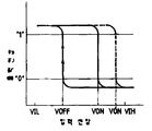
제 2 도는 제 1 도에 도시된 입력회로의 입출력특성을 나타낸 도면.2 is a diagram showing input / output characteristics of the input circuit shown in FIG.
제 3 도는 제 1 도에 도시된 입력회로의 입력잡음과 임계치전압사이의 관계를 나타낸 도면.3 is a diagram showing the relationship between the input noise and the threshold voltage of the input circuit shown in FIG.
제 4 도는 제 1 도에 도시된 입력회로에서 제어신호를 발생시키는 회로의 실제적인 구성예를 나타낸 도면.4 is a diagram showing an actual configuration example of a circuit for generating a control signal in the input circuit shown in FIG.
제 5 도는 제 4 도에 도시된 제어신호발생회로의 동작을 설명하기 위한 타이밍 챠트.5 is a timing chart for explaining the operation of the control signal generation circuit shown in FIG.
제 6 도는 본 발명에 따른 반도체집적회로에서의 입력회로의 제2실시예를 나타낸 도면.6 is a view showing a second embodiment of an input circuit in a semiconductor integrated circuit according to the present invention.
제 7 도는 제 6 도에 도시된 입력회로의 입출력특성을 나타낸 도면.7 is a diagram showing input / output characteristics of the input circuit shown in FIG.
제 8 도는 제 6 도에 도시된 입력회로의 입력잡음과 임계치전압사이의 관계를 나타낸 도면.8 is a diagram showing the relationship between the input noise and the threshold voltage of the input circuit shown in FIG.
제 9 도는 본 발명에 따른 반도체집적회로에서의 입력회로의 제3실시예를 나타낸 회로도이다.9 is a circuit diagram showing a third embodiment of the input circuit in the semiconductor integrated circuit according to the present invention.
* 도면의 주요부분에 대한 부호의 설명* Explanation of symbols for main parts of the drawings
10 : 칩 12 : 입력회로10: chip 12: input circuit
14 : 내부회로 16 : 출력회로14: internal circuit 16: output circuit
18 : 제어신호발생회로 161 : 출력버퍼18: control signal generation circuit 161: output buffer
VDD : 전원 VSS : 접지VDD: Power VSS: Ground
Q1∼Q6, Q11∼Q15 : MOS FET C : 캐패시터Q1 to Q6, Q11 to Q15: MOS FET C: Capacitor
VOUT : 신호출력단자 VIN : 입력신호VOUT: Signal Output Terminal VIN: Input Signal
ø : 제어신호 VON,VOFF,VOFF´ : 임계치전압ø: Control signal VON, VOFF, VOFF´: Threshold voltage
RAS : 행어드레스스트로브신호 CAS : 열어드레스스트로브신호RAS: Hang address strobe signal CAS: Open address strobe signal
OE1,![]()
![]()
WE : 기록이네이블신호WE: Record enable signal
본 발명은 반도체집적회로에 관한 것으로, 특히 전원잡음에 의한 회로의 오동작을 방지하는 기능을 갖춘 반도체집적회로에 관한 것이다.BACKGROUND OF THE INVENTION 1. Field of the Invention The present invention relates to a semiconductor integrated circuit, and more particularly, to a semiconductor integrated circuit having a function of preventing malfunction of a circuit due to power supply noise.
반도체집적회로의 동작중에는 회로의 전원선(예컨대 공급전원선과 접지선)을 통해서 전류가 흐르게 되는데, 이 전류가 큰 경우에는 전원전위가 변동하게 된다. 이러한 전원전위의 변동은 회로의 오동작을 초래하므로 전원잡음이라 불리워진다.During the operation of the semiconductor integrated circuit, a current flows through the power supply line (for example, the supply power supply line and the ground line) of the circuit. When this current is large, the power supply potential changes. Such fluctuations in power supply potential cause circuit malfunction, which is called power supply noise.
즉, 입출력데이터가 다비트로 구성된 반도체메모리와 같은 반도체집적회로에 있어서는 기억된 데이터를 독출하기 위해 각 출력버퍼로부터 "1"레벨이 출력되거나 또는 각 출력버퍼로부터"0"레벨이 출력되는 경우에 전원잡음이 발생하게 되는바, 각 출력버퍼에서 "1"레벨이 출력되는 경우에는 전원선으로부터 부하로 공급되는 전하의 공급타이밍이 지연되어 전원선의 전위가 급속히 낮아지게 되고, 이와는 달리 각 출력버퍼로부터 "0"레벨이 출력되는 경우에는 접지선의 전위가 급속히 높아지게 된다. 그리고 전원선과 접지선 사이에는 용량성분이 존재하므로 전원선의 전위가 결합에 의한 영향으로 갑자기 감소한 경우에는 접지선의 전위도 감소하게 되고, 역으로 접지선의 전위가 갑자기 증가한 경우에는 전원선의 전위도 그에 따라 증가하게 된다.That is, in a semiconductor integrated circuit such as a semiconductor memory having a multi-bit input / output data, when the "1" level is output from each output buffer or the "0" level is output from each output buffer in order to read the stored data. When the "1" level is output from each output buffer, the timing of supply of charge from the power supply line to the load is delayed, and the potential of the power supply line is rapidly lowered. When the 0 "level is output, the potential of the ground wire becomes high rapidly. Since the capacitive component exists between the power line and the ground line, if the potential of the power line suddenly decreases due to the coupling, the potential of the ground line also decreases. On the contrary, if the potential of the ground line suddenly increases, the potential of the power line increases accordingly. do.
또한, 반도체집적회로의 경우에는 칩상에 형성된 모든 회로(입력회로, 내부회로, 출력회로)는 전원선에 공통으로 접속되어 있기 때문에 출력버퍼의 구동을 통해 발생된 전원잡음은 입력회로에서 검출된 입력신호의 레벨을 변화시키게 된다. 따라서 입력신호에 잡음이 포함되지 않는 경우에도 입력회로는 잡음을 포함한 것처럼 동작하게 된다.In the case of a semiconductor integrated circuit, since all circuits (input circuits, internal circuits, and output circuits) formed on the chip are commonly connected to the power supply line, power noise generated by driving the output buffer is detected by the input circuit. This will change the level of the signal. Therefore, even if noise is not included in the input signal, the input circuit operates as if it contains noise.
즉, "0"레벨의 입력신호가 입력회로로 공급되는 동안 전원선 및 접지선의 전위를 낮추는 전원잡음이 되는 경우에는 입력신호의 전위가 명백히 상승하게 되므로 입력회로는 이 신호를 "1"레벨의 신호로서 검출하게 되고, 역으로 "1"레벨의 입력신호가 입력회로로 공급되는 동안 전원잡음이 발생되는 경우에는 입력신호의 저위가 분명히 낮아지게 되므로 입력회로는 이 신호를 "0"레벨의 신호로서 검출하게 된다.That is, when the input noise of the "0" level becomes the power supply noise that lowers the potentials of the power supply line and the ground line while the input signal is supplied to the input circuit, the potential of the input signal is raised so that the input circuit raises this signal to the "1" level. When the power source noise is generated while the input signal of the "1" level is supplied to the input circuit, the input signal is clearly lowered. Therefore, the input circuit detects this signal as the "0" level signal. Will be detected as
따라서 통상 입력회로는 쉬미트트리거회로로 구성하여 상기한 입력신호의 오검출이 일어나지 않도록 하고 있다. 이러한 쉬미트트리거회로는 각각 다른 2개의 임계치전압(VON, VOFF)을 갖추고 있는데, 그중 제1전압(VON)은 입력신호가 "0"레벨로부터 "1"레벨로 상승하는 것을 검출하는데 사용되고, 제2전압(VOFF)은 입력신호가 "1"레벨로부터 "0"레벨로 강하되는 것을 검출하는데 사용된다. 잘알려진 바와 같이 쉬미트트리거회로는 히스테리시스 입출력특성을 갖는다.Therefore, the normal input circuit is constituted by the Schmitt trigger circuit so that the above error detection of the input signal does not occur. The Schmitt trigger circuit has two different threshold voltages VON and VOFF, respectively, of which the first voltage VON is used to detect the rising of the input signal from the " 0 " level to the " 1 " level. The two voltages VOFF are used to detect that the input signal falls from the "1" level to the "0" level. As is well known, the Schmitt trigger circuit has hysteresis input and output characteristics.
입력회로를 쉬미트트리거회로로 구성하는 경우에는 다음과 같은 이점을 얻을 수 있다. 즉, 전원잡음이 쉬미트트리거회로의 히스테리시스전압(=VON-VOFF)보다 대체로 작은 경우에는 회로의 오동작이 발생되지 않으므로, 히스테리시스전압이 높으면 높을수록 더 큰 입력회로의 잡음에 견딜 수 있게 된다. 그러나, 만일 입력회로의 히스테리시스전압이 소정값을 넘게 되면 입력신호의 동작마진이 감소하게 되므로, 히스테리시스전압을 소정값 이상으로 할 수 없게 된다. 따라서, 전원잡음이 큰 경우에는 입력회로의 오동작이 초래되게 되는 결점이 있다.When the input circuit is composed of the Schmitt trigger circuit, the following advantages can be obtained. That is, when the power supply noise is generally smaller than the hysteresis voltage (= VON-VOFF) of the Schmitt trigger circuit, no malfunction of the circuit occurs. Therefore, the higher the hysteresis voltage, the more the noise of the larger input circuit can be tolerated. However, if the hysteresis voltage of the input circuit exceeds a predetermined value, the operating margin of the input signal is reduced, so that the hysteresis voltage cannot be made higher than the predetermined value. Therefore, there is a drawback that the malfunction of the input circuit is caused when the power supply noise is large.
이에 본 발명은, 상기한 실정을 감안하여 발명된 것으로, 전원잡음이 발생되더라도 정확하게 동작할 수 있고, 입력신호에 대해 큰 동작마진을 갖는 반도체집적회로를 제공함에 그 목적이 있다.Accordingly, the present invention has been made in view of the above-described situation, and an object thereof is to provide a semiconductor integrated circuit which can operate accurately even when power noise is generated and has a large operating margin for an input signal.
상기한 목적을 달성하기 위한 본 발명의 반도체집적회로는 하나의 단일 칩상에 형성됨과 더불어 모두 공통전원선에 접속된 입력회로와 내부회로 및 출력회로를 갖추고; 상기 입력회로는 전원선과 신호출력단자 사이에 위치된 부하회로와, 상기 신호출력단자와 접지선사이에 직렬로 접속됨과 더불어 각각의 게이트에 입력신호가 공급되는 서로 동일 도전형인 제1 및 제2FET, 일단이 전원선에 접속됨과 더불어 다른 단이 상기 제1 및 제2FET의 직렬접속점에 접속되고 게이트가 상기 신호출력단자에 접속되는 제3FET, 일단의 소정의 전위가 공급됨과 더불어 다른 단이 상기 제1 및 제2FET의 직렬접속점에 접속되어서 전원선과 접지선의 전위가 내부회로 및 출력회로의 동작에 따라 변동할 때 제어신호에 의해 소정시간구간동안 턴온되는 제4FET를 포함하는 구성으로 되어 있다.The semiconductor integrated circuit of the present invention for achieving the above object is formed on one single chip and has an input circuit, an internal circuit, and an output circuit all connected to a common power line; The input circuit includes a load circuit positioned between a power supply line and a signal output terminal, and first and second FETs having the same conductivity type, which are connected in series between the signal output terminal and the ground line, and in which an input signal is supplied to each gate. A third FET connected to the power supply line, the other end of which is connected to the series connection point of the first and second FETs, and the gate of which is connected to the signal output terminal; The fourth FET is connected to the series connection point of the second FET and includes a fourth FET which is turned on for a predetermined time period by a control signal when the potential of the power supply line and the ground line changes with the operation of the internal circuit and the output circuit.
이하, 도면을 참조해서 본 발명의 실시예를 설명한다.Hereinafter, embodiments of the present invention will be described with reference to the drawings.
제 1 도는 본 발명에 따른 반도체집적회로에 설치되는 입력회로의 제1실시예를 나타낸 것으로서, 이 입력회로는 하나의 칩상에 내부회로 및 출력회로와 함께 형성되게 되고, 이 모든 3개의 회로(입력회로, 내부회로, 출력회로)는 공통전원선[전원(VDD)선, 접지(VSS)선]에 접속되게 된다.1 shows a first embodiment of an input circuit installed in a semiconductor integrated circuit according to the present invention, which is formed together with an internal circuit and an output circuit on one chip, and all three circuits (input The circuit, the internal circuit, and the output circuit) are connected to a common power supply line (power supply VDD line, ground VSS line).
제 1 도에 도시된 바와같이 입력회로는 캐패시터(C)와 N형 MOS FET(Q1∼Q6)로 구성되어 있다. 여기서 캐패시터(C)와 MOS FET(Q1,Q2)는 서로 접속되어부스트랩(bootstrap)형 부하회로를 구성하고 있는 데, 이 부하회로는 전원(VDD)선과 신호출력단자(VOUT)사이에 접속되고, 또 신호출력단자(VOUT)와 접지(VSS)선 사이에는 MOS FET(Q3,Q4)의 소오스-드레스 통로가 직렬로 접속되어 입력신호(VIN)가 외부적으로 그 MOS FET(Q3,Q4)의 게이트로 공급되도록 되어 있다. 그리고 MOS FET(Q5)는 그 일단이 전원(VDD)선에 접속되면서 다른 단은 MOS FET(Q3, Q4)의 접속점에 접속되고, 그 게이트는 신호 출력단자(VOUT)에 접속되어 있다. 또한 MOS FET(Q6)는 그 일단이 전원(VDD)선에 접속되면서 다른 단은 상기 MOS FET(Q3,Q4)의 접속점에 접속되고, 그 게이트에 제어신호(![]()
![]()
상기한 바와같이 구성된 입력회로에 있어서, MOS FET(Q5)는 출력단자(VOUT)의 전위에 따라 제어되고 MOS FET(Q3,Q4)의 접속점에서의 전위는 MOS FET(Q5)의 동작상태에 따라 변하게 된다. 따라서 입력회로는 제 2 도에 실선으로 도시된 바와같은 히스테리시스특성을 갖게 된다.In the input circuit configured as described above, the MOS FET Q5 is controlled in accordance with the potential of the output terminal VOUT, and the potential at the connection point of the MOS FETs Q3 and Q4 is dependent on the operating state of the MOS FET Q5. Will change. Therefore, the input circuit has hysteresis characteristics as shown by the solid line in FIG.
한편, 전원잡음이 발생되는 소정기간동안 제어신호(![]()
![]()
그러므로 입력신호(VIN)의 "0"레벨이 검출될 때 접지전위(VSS)를 저하시키는 전원잡음이 발생되어 제 3 도에 도시된 바와같이 잡음이 "0"레벨의 입력신호(VIN)에 혼합되더라도 입력신호를 정확하게 검출할수 있게 된다. 따라서 내부회로의 오동작을 장지할 수 있게 된다.Therefore, when the "0" level of the input signal VIN is detected, a power noise that lowers the ground potential VSS is generated, and noise is mixed with the input signal VIN of the "0" level as shown in FIG. Even if the input signal can be detected accurately. Therefore, malfunction of the internal circuit can be prevented.
한편, 제어신호(![]()
![]()
따라서 이러한 회로를 제 1 도에 도시된 반도체메모리의 입력회로로 사용하게 되면 출력버퍼의 구동중에 대체로 "0"레벨이 보상되는 열어드레스스트로브신호(CAS)나 행어드레스스트로브신호(RAS)의 입력회로로서 효과적이게 된다.Therefore, when such a circuit is used as the input circuit of the semiconductor memory shown in FIG. 1, the input circuit of the open address strobe signal CAS or the row address strobe signal RAS whose level is substantially compensated during the driving of the output buffer. As effective.
상기한 바와같이 전원잡음은 저원(VDD)선으로부터 큰 전류가 흘러나올때와 접지(VSS)선으로 큰 전류가 흐를 때 발생되므로, 제어신호(![]()
![]()
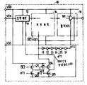
제 4 도는 출력버퍼를 활성화시키는 신호(OE1)에 따라 소정기간동안 "1"레벨의 제어신호(![]()
![]()
또한, 상기 제어신호발생회로(18)는 종속접속된 6개의 인버터(Ⅰ1~Ⅰ6)와, 5개의 N형 MOS FET(Q11~Q15)로 구성된다. 여기서 FET(Q11,Q12)는 각 소오스와 드레인사이 전류통로가 전원(VDD)선과 접지(VSS)선 사이에 직렬로 접속되면서, MOS FET(Q11,)의 게이트에는 신호(![]()
![]()
![]()
![]()
![]()
![]()
![]()
![]()
또한 신호(OE1)는 종속접속된 인버터중 제 1단 인버터(Ⅰ1)의 입력단자로 공급되어 신호(![]()
![]()
![]()
![]()
그리고 출력버퍼(Ⅰ61)가 활성화될 때 내부회로 (14)로부터 출력되는 신호 (OE1)는 "0"레벨로부터 "1"레벨로 상승하게 되고, 신호(![]()
![]()
![]()
![]()
![]()
![]()
그러므로 제어신호발생회로(18)에 있어서 MOS FET(Q14,Q15)의 접속점으로부터 출력되는 제어신호(![]()
![]()
![]()
![]()
제 6 도는 본 발명의 제 2 실시예에 따른 입력회로는 도시해 놓은 것으로서, 이 입력회로는 제 1 도에 도시된 입력회로와 유사한 방법으로 일단이 N형 MOS FET(Q3,Q4)의 접속점에 접속된 N형 MOS FET(Q6)의 게이트로 제어신호(![]()
![]()
상기한 구성으로 된 입력회로에 있어서, 제어신호(![]()
![]()
그러므로 입력신호(VIN)의 "1"레벨이 검출될 때 접지전위(VSS)를 상승시키는 전원잡음이 발생하여 "1"레벨의 입력신호(VIN)에 제 8 도에 도시한 바와같은 잡음이 혼합되더라도, VOFF가 VOFF'로 낮아져서 회로의 오동작을 방지할 수 있게 된다.Therefore, when the "1" level of the input signal VIN is detected, a power noise that raises the ground potential VSS occurs, and the noise as shown in FIG. 8 is mixed with the input signal VIN of the "1" level. Even if the VOFF is lowered to VOFF ', malfunction of the circuit can be prevented.
따라서, 상기한 입력회로는 출력버퍼의 구동중에 통상 "1"레벨로 되는 기록이네이블신호(WE) 의 검출회로로서도 유효하게 된다.Therefore, the above-described input circuit is also effective as a detection circuit for the write enable signal WE which normally becomes " 1 " level while driving the output buffer.
제 9 도는 본 발명의 제3실시예에 따른 입력회로를 되시해 놓은것으로서, 이 입력회로에 있어서는 제 1 도에 도시된 회로에 부가해서 N형 MOS FET(Q7)가 MOS FET(Q3,Q4)의 접속점과 MOS FET(Q6)의 일단사이에 삽입되어 있는바, 이 MOS FET(Q7)의 스위칭동작은 신호입출력단자의 전위로 제어되게 된다.9 shows an input circuit according to the third embodiment of the present invention. In this input circuit, in addition to the circuit shown in FIG. 1, an N-type MOS FET Q7 is connected to the MOS FETs Q3 and Q4. The switching operation of the MOS FET Q7 is controlled by the potential of the signal input / output terminal, which is inserted between the connection point of the MOS FET Q6 and one end of the MOS FET Q6.
이와같은 구성에 의하면 입력신호(VIN)가 "0"레벨에서 "1"레벨로 상승하기 시작하면, 신호출력단자의 전위가 낮아지기 시작하면서 트랜지스터(Q7)가 턴오프상태로 되어 MOS FET(Q6)에 의한 전하공급이 차단된다. 그러므로 이 회로에서는 입력신호가 "1"레벨에서 "0"레벨로 전위하는 도중에 제어신호(![]()
![]()
더욱이 전원잡음이 발생되는 것은 출력버퍼의 구동시에만 한정되지 않고 예컨대 메모리 회로에서 비트선을 선충전시킬때에도 전원잡음이 발생되므로 제어신호 (![]()
![]()
Claims (9)
Applications Claiming Priority (3)
| Application Number | Priority Date | Filing Date | Title |
|---|---|---|---|
| JP70766 | 1987-03-25 | ||
| JP62070766A JPS63236407A (en) | 1987-03-25 | 1987-03-25 | Semiconductor circuit |
| JP62-70766 | 1987-03-25 |
Publications (2)
| Publication Number | Publication Date |
|---|---|
| KR880011805A KR880011805A (en) | 1988-10-31 |
| KR910003603B1 true KR910003603B1 (en) | 1991-06-07 |
Family
ID=13440965
Family Applications (1)
| Application Number | Title | Priority Date | Filing Date |
|---|---|---|---|
| KR1019880003238A KR910003603B1 (en) | 1987-03-25 | 1988-03-25 | Schmitt input type semiconductor integrated circuit |
Country Status (3)
| Country | Link |
|---|---|
| US (1) | US4893029A (en) |
| JP (1) | JPS63236407A (en) |
| KR (1) | KR910003603B1 (en) |
Families Citing this family (11)
| Publication number | Priority date | Publication date | Assignee | Title |
|---|---|---|---|---|
| JP2542678B2 (en) * | 1988-06-17 | 1996-10-09 | 富士通株式会社 | Semiconductor device |
| KR910007740B1 (en) * | 1989-05-02 | 1991-09-30 | 삼성전자 주식회사 | Power voltage tracking circuit for bit line stabilization |
| US5243232A (en) * | 1991-07-31 | 1993-09-07 | Allen-Bradley Company, Inc. | Start-up pulse suppression circuit for industrial controller output |
| US5442304A (en) * | 1993-10-15 | 1995-08-15 | Advanced Micro Devices, Inc. | CMOS logic gate clamping circuit |
| JP2822881B2 (en) * | 1994-03-30 | 1998-11-11 | 日本電気株式会社 | Semiconductor integrated circuit device |
| EP0724209A1 (en) * | 1995-01-25 | 1996-07-31 | International Business Machines Corporation | Power management system for integrated circuits |
| IT1312498B1 (en) * | 1999-05-13 | 2002-04-17 | St Microelectronics Srl | INTEGRATED STRUCTURE WITH ANALOGUE UNIT SUPPLIED BY VOLTAGE EXTERNAL POWER SUPPLY THROUGH LOW-PASS FILTER AND ELEMENTS OF |
| DE19936606C1 (en) * | 1999-08-04 | 2000-10-26 | Siemens Ag | Integrated circuit voltage supply via pad e.g. for microprocessors and microcontrollers |
| US6320408B1 (en) | 2001-03-02 | 2001-11-20 | Pericom Semiconductor Corp. | Dual-sided undershoot-isolating bus switch |
| US7514951B2 (en) * | 2005-09-20 | 2009-04-07 | Etron Technology, Inc. | Negative voltage noise-free circuit for multi-functional pad |
| JP4940643B2 (en) * | 2005-12-08 | 2012-05-30 | 日本電気株式会社 | Power supply noise tolerance inspection circuit and power supply noise tolerance inspection method |
Family Cites Families (3)
| Publication number | Priority date | Publication date | Assignee | Title |
|---|---|---|---|---|
| JPS57183119A (en) * | 1981-05-02 | 1982-11-11 | Sanyo Electric Co Ltd | Schmitt circuit |
| JPS5877317A (en) * | 1981-11-02 | 1983-05-10 | Matsushita Electric Ind Co Ltd | Schmitt tigger circuit |
| US4707626A (en) * | 1984-07-26 | 1987-11-17 | Texas Instruments Incorporated | Internal time-out circuit for CMOS dynamic RAM |
-
1987
- 1987-03-25 JP JP62070766A patent/JPS63236407A/en active Granted
-
1988
- 1988-03-14 US US07/167,687 patent/US4893029A/en not_active Expired - Lifetime
- 1988-03-25 KR KR1019880003238A patent/KR910003603B1/en not_active IP Right Cessation
Also Published As
| Publication number | Publication date |
|---|---|
| JPH0470805B2 (en) | 1992-11-12 |
| US4893029A (en) | 1990-01-09 |
| JPS63236407A (en) | 1988-10-03 |
| KR880011805A (en) | 1988-10-31 |
Similar Documents
| Publication | Publication Date | Title |
|---|---|---|
| US5204837A (en) | Semiconductor memory device having test mode | |
| US5220221A (en) | Sense amplifier pulldown circuit for minimizing ground noise at high power supply voltages | |
| US4972100A (en) | Data output buffer circuit for byte-wide memory | |
| US4985644A (en) | Output buffer semiconductor and method for controlling current flow in an output switching device | |
| US5583460A (en) | Output driver circuit for restraining generation of noise and semiconductor memory device utilizing such circuit | |
| US4873673A (en) | Driver circuit having a current mirror circuit | |
| KR910003603B1 (en) | Schmitt input type semiconductor integrated circuit | |
| EP0052010A1 (en) | Buffer amplifier circuit and address buffer circuit using such buffer amplifier circuit | |
| JPH0113657B2 (en) | ||
| US4366397A (en) | Level conversion circuit | |
| KR920010824B1 (en) | Semiconductor memory | |
| KR950005171B1 (en) | Current mirror amplifier and driving method | |
| US5953279A (en) | Fuse option circuit for memory device | |
| US4554469A (en) | Static bootstrap semiconductor drive circuit | |
| US5463335A (en) | Power up detection circuits | |
| US4896056A (en) | Semiconductor IC including circuit for preventing erroneous operation caused by power source noise | |
| KR960000896B1 (en) | Semiconductor integrated circuit device | |
| EP0148364B1 (en) | Timing signal generator | |
| US20010035779A1 (en) | Low-noise buffer circuit | |
| JP3192751B2 (en) | Semiconductor device | |
| US20060202724A1 (en) | Comparator circuit assembly, in particular for semiconductor components | |
| US5796674A (en) | Signal transition detection circuit | |
| US20030101374A1 (en) | Semiconductor device with reduced terminal input capacitance | |
| JP2851211B2 (en) | Input buffer circuit | |
| US5565802A (en) | Semiconductor device with differential amplifier operable at high speed |
Legal Events
| Date | Code | Title | Description |
|---|---|---|---|
| A201 | Request for examination | ||
| E902 | Notification of reason for refusal | ||
| G160 | Decision to publish patent application | ||
| E701 | Decision to grant or registration of patent right | ||
| GRNT | Written decision to grant | ||
| FPAY | Annual fee payment |
Payment date: 20030530 Year of fee payment: 13 |
|
| LAPS | Lapse due to unpaid annual fee |