EP0052010A1 - Buffer amplifier circuit and address buffer circuit using such buffer amplifier circuit - Google Patents
Buffer amplifier circuit and address buffer circuit using such buffer amplifier circuit Download PDFInfo
- Publication number
- EP0052010A1 EP0052010A1 EP81305327A EP81305327A EP0052010A1 EP 0052010 A1 EP0052010 A1 EP 0052010A1 EP 81305327 A EP81305327 A EP 81305327A EP 81305327 A EP81305327 A EP 81305327A EP 0052010 A1 EP0052010 A1 EP 0052010A1
- Authority
- EP
- European Patent Office
- Prior art keywords
- transistor
- buffer amplifier
- amplifier circuit
- inverter
- circuit
- Prior art date
- Legal status (The legal status is an assumption and is not a legal conclusion. Google has not performed a legal analysis and makes no representation as to the accuracy of the status listed.)
- Granted
Links
Images


Classifications
-
- H—ELECTRICITY
- H03—ELECTRONIC CIRCUITRY
- H03K—PULSE TECHNIQUE
- H03K19/00—Logic circuits, i.e. having at least two inputs acting on one output; Inverting circuits
- H03K19/02—Logic circuits, i.e. having at least two inputs acting on one output; Inverting circuits using specified components
- H03K19/08—Logic circuits, i.e. having at least two inputs acting on one output; Inverting circuits using specified components using semiconductor devices
- H03K19/094—Logic circuits, i.e. having at least two inputs acting on one output; Inverting circuits using specified components using semiconductor devices using field-effect transistors
- H03K19/0944—Logic circuits, i.e. having at least two inputs acting on one output; Inverting circuits using specified components using semiconductor devices using field-effect transistors using MOSFET or insulated gate field-effect transistors, i.e. IGFET
- H03K19/09441—Logic circuits, i.e. having at least two inputs acting on one output; Inverting circuits using specified components using semiconductor devices using field-effect transistors using MOSFET or insulated gate field-effect transistors, i.e. IGFET of the same canal type
- H03K19/09443—Logic circuits, i.e. having at least two inputs acting on one output; Inverting circuits using specified components using semiconductor devices using field-effect transistors using MOSFET or insulated gate field-effect transistors, i.e. IGFET of the same canal type using a combination of enhancement and depletion transistors
-
- G—PHYSICS
- G11—INFORMATION STORAGE
- G11C—STATIC STORES
- G11C8/00—Arrangements for selecting an address in a digital store
- G11C8/06—Address interface arrangements, e.g. address buffers
-
- H—ELECTRICITY
- H03—ELECTRONIC CIRCUITRY
- H03K—PULSE TECHNIQUE
- H03K19/00—Logic circuits, i.e. having at least two inputs acting on one output; Inverting circuits
- H03K19/01—Modifications for accelerating switching
- H03K19/017—Modifications for accelerating switching in field-effect transistor circuits
- H03K19/01707—Modifications for accelerating switching in field-effect transistor circuits in asynchronous circuits
- H03K19/01721—Modifications for accelerating switching in field-effect transistor circuits in asynchronous circuits by means of a pull-up or down element
-
- H—ELECTRICITY
- H03—ELECTRONIC CIRCUITRY
- H03K—PULSE TECHNIQUE
- H03K19/00—Logic circuits, i.e. having at least two inputs acting on one output; Inverting circuits
- H03K19/0175—Coupling arrangements; Interface arrangements
- H03K19/0185—Coupling arrangements; Interface arrangements using field effect transistors only
- H03K19/018507—Interface arrangements
Definitions
- the present invention relates to a buffer amplifier circuit which has a high operating speed and which is used, for example, as an address buffer circuit of a semiconductor memory device.
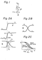
- Fig. 1 illustrates a conventional buffer amplifier circuit which is used, for example, as an input buffer circuit such as an address buffer circuit of a semiconductor memory device.
- the buffer amplifier circuit of Fig. 1 has an inverter structure and comprises a series connection of an N-channel enhancement type MI S driver transistor Ql and an N-channel depletion type MIS load transistor Q2.
- A designates an input signal
- B designates an output signal
- Vcc designates a power supply voltage.
- an internal logic signal A' of a MIS integrated circuit generally has a high potential level (H) of 5 V and a low potential level (L) of 0 V and, therefore, has an amply large amplitude for driving the inverter circuit of Fig. 1.
- the input signal to the MIS integrated circuit is transferred through printed circuit patterns and/or lead wires, from a TTL circuit for example, the input signal is attenuated and the amplitude thereof becomes smaller.
- the actual input signal has oscillations.
- the effective high potential level of the input signal becomes, for example, 2 V and the effective low potential level of the input signal becomes, for example, 0.8 V.
- the operating speed of the inverter circuit becomes slow, i.e., the switching time of the output signal B between the high and low potential levels becomes long and, in the worst case, the switching operation between the high and low potential levels is not effected correctly.
- the operating speed of the inverter circuit of Fig. 1 is also influenced by the gm characteristics of the transistors Ql and Q2.
- the rise time from the low potential level L to the high potential level H and the fall time from the high potential level to the low potential level of the output signal B are nearly equal to each other as illustrated in Fig. 2B.
- the operating speed of such an inverter circuit cannot be fast. If the gm ratio of the transistors Ql and Q2, i.e., the ratio of the gm of the transistor Ql to the gm of the transistor Q2 becomes smaller than 1, the rise time of the output signal B becomes short and the fall time of the output signal B becomes long as illustrated by solid lines Cl of Fig. 2A.
- the gm ratio also influences the threshold potential level Vth of the input signal A of the inverter circuit of Fig. 1.
- V threshold potential level
- Fig. 2C in order to gain the high threshold potential level V"th, it is necessary to make the gm ratio smaller, and, in order to gain the low threshold potential level V'th, it is necessary to make the gm ratio larger. Since it is necessary to adjust the threshold potential-Vth to an appropriate level according to the potential levels of the 'input signal and according to the structure of the pre-stage circuit (e.g. TTL or MIS circuit) connected to the inverter circuit of Fig. 1, the gm ratio and, therefore, the operation speed of the conventional buffer amplifier are limited by the potential levels of the input signal.
- the driver transistor Ql is overdriven by the input signal and the operation speed of the inverter circuit of Fig. 1 can be fast.
- Fig. 3 illustrates a conventional address buffer circuit of a semiconductor memory device which uses the buffer amplifier circuits of F ig. 1.
- the address buffer circuits of Fig. 3 comprises the first, the second and the third inverter circuits INV1, INV2 and INV3 which consist of MIS transistors Q3, Q4; Q5, Q6 and Q7, Q8, respectively, and each of which has the same circuit structure as that of the inverter circuit of Fig. 1.
- the address buffer circuit of Fig. 3 further comprises two output buffer amplifiers BA1 and BA2 which consist of MIS transistors Q9, Q10 and Qll, Q12, respectively and which output buffered address signals A and A 0 , respectively.
- the principal object of the present invention to provide a buffer amplifier circuit having a high operating speed.
- a buffer amplifier circuit comprising a first inverter including a first driver transistor whose gate electrode receives an input signal; a second inverter including a second driver transistor whose gate electrode receives an output signal from the first inverter and whose source electrode is commonly connected to the source electrode of the first driver transistor; and a control transistor whose drain electrode is connected to the commonly connected source electrodes of the first and second driver transistors and which changes the potential of the commonly connected source electrodes so as to enlarge upon a change in potential difference between the gate and source electrodes of the first driver transistor when the potential level of the input signal is changed.
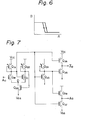
- Figure 4 illustrates an inverter type buffer amplifier circuit as an embodiment of the present invention.
- the buffer amplifier circuit of Figure 4 comprises a first inverter including a driver transistor Q13 and a load transistor Q14, a second inverter including a driver transistor Q15 and a load transistor Q16, and, a control transistor Q17.
- the source electrodes of the driver transistors Q13 and Q15 are commonly connected to the drain electrode of the control transistor Q17.
- Both the load transistors Q14 and Q16 are depletion type MIS transistors and the other transistors Q13, Q15 and Q17 are all enhancement type MIS transistors.
- the output terminal of the first inverter i.e., the drain electrode of the transistor Q13 is connected to the input terminal of the second inverter, i.e., the gate electrode of the transistor Q15.
- the output terminal of the second inverter i.e., the drain electrode of the transistor Q15 is connected to the gate electrode of the control transistor Q1 7 .
- the operation of the buffer amplifier circuit of Figure 4 will now be described. Assume that the input signal A is to be changed from low level, e.g. 0.8 V, to high level, e.g. 2.0 V. In this case, as transistor Q13 is turned on, as the level of input signal A changes, the output signal B changes from high level, e.g. 5 V, towards low level, e.g. 0.7 V. As the transistor Q13 turns on the transistor Q15 turns off and the output signal C of the second inverter becomes higher, e.g. increases towards 5 V.
- the transistor Q17 is turned on and the potential D of the drain electrode of the transistor Q17 to which the sourceU electrodes of the transistors Q13 and Q15 are connected becomes low, e.g. 0 V. Therefore, the input potential applied between the gate and source electrodes of the transistor Q13 is enlarged and the turning-on of the transistor Q13 is accelerated.
- the threshold potential of the input signal A can be determined by the gm ratio of the transistors Q13 and Q14 to any appropriate value according to the potential levels of the input signal A without affecting the operating speed of the buffer amplifier circuit.
- Figure 6 illustrates an input-output characteristic of the buffer amplifier circuit of Figure 4. Since the potential D of the drain electrode of the control transistor Q17 changes in an opposite direction to that of the input signal A, the relation between the input signal A and the output signal B shows a hysteresis characteristic.
- Figure 7 illustrates an address buffer circuit which is used in a semiconductor memory device and which includes a buffer amplifier circuit according to the present invention.
- the address buffer circuit of Fig. 7 comprises an input buffer amplifier stage which includes MIS transistors Q18 through Q22 and which has the same circuit structure as that of the buffer amplifier circuit of Figure 4, and an output buffer stage which includes MIS transistors Q23 through Q28 and which has the same circuit structure as that of the output buffer stage of the circuit of Fig. 3 including the inverter INV3 and the buffer amplifiers BA1 and BA2.
- the operation of the address buffer circuit is apparent from the above description, and therefore the explanation thereof is omitted here.
- the signal delay time of the output address signals A 0 and A 0 can be very small and the threshold potential of the input address signal A 0 can be selected to an appropriate value according to the potential levels of the input address signal A O .
- the present invention it is possible to increase the operation speed of the inverter type buffer amplifier circuit, by using a simple circuitry including the control MIS transistor which enlarges the change of the input potential applied between the gate and the source electrodes of the driver transistor.
Landscapes
- Engineering & Computer Science (AREA)
- Computer Hardware Design (AREA)
- Physics & Mathematics (AREA)
- Computing Systems (AREA)
- General Engineering & Computer Science (AREA)
- Mathematical Physics (AREA)
- Power Engineering (AREA)
- Microelectronics & Electronic Packaging (AREA)
- Logic Circuits (AREA)
- Static Random-Access Memory (AREA)
Abstract
Description
- The present invention relates to a buffer amplifier circuit which has a high operating speed and which is used, for example, as an address buffer circuit of a semiconductor memory device.
- Fig. 1 illustrates a conventional buffer amplifier circuit which is used, for example, as an input buffer circuit such as an address buffer circuit of a semiconductor memory device. The buffer amplifier circuit of Fig. 1 has an inverter structure and comprises a series connection of an N-channel enhancement type MIS driver transistor Ql and an N-channel depletion type MIS load transistor Q2. In Fig. 1, A designates an input signal, B designates an output signal and Vcc designates a power supply voltage.
- In the buffer amplifier circuit of Fig. 1, when the potential of the input signal A becomes high, the N-channel MIS transistor Ql is turned on and the output signal B becomes low. On the contrary, when the potential of the input signal A becomes low, the transistor Ql is turned off and the output signal B becomes high. However, such an operation is guaranteed only in the condition when the input signal A has an amply high potential level and an amply low potential level and in the steady state condition.
- As illustrated in Fig. 2A, an internal logic signal A' of a MIS integrated circuit generally has a high potential level (H) of 5 V and a low potential level (L) of 0 V and, therefore, has an amply large amplitude for driving the inverter circuit of Fig. 1. However, since the input signal to the MIS integrated circuit is transferred through printed circuit patterns and/or lead wires, from a TTL circuit for example, the input signal is attenuated and the amplitude thereof becomes smaller. Moreover, as shown by Aa in Fig. 2A, the actual input signal has oscillations.
- Therefore, the effective high potential level of the input signal becomes, for example, 2 V and the effective low potential level of the input signal becomes, for example, 0.8 V. When such input signal is applied to the inverter circuit of Fig. 1, the operating speed of the inverter circuit becomes slow, i.e., the switching time of the output signal B between the high and low potential levels becomes long and, in the worst case, the switching operation between the high and low potential levels is not effected correctly. The operating speed of the inverter circuit of Fig. 1 is also influenced by the gm characteristics of the transistors Ql and Q2. For example, when the gms of the transistors Ql and Q2 are equal to each other, the rise time from the low potential level L to the high potential level H and the fall time from the high potential level to the low potential level of the output signal B are nearly equal to each other as illustrated in Fig. 2B. However the operating speed of such an inverter circuit cannot be fast. If the gm ratio of the transistors Ql and Q2, i.e., the ratio of the gm of the transistor Ql to the gm of the transistor Q2 becomes smaller than 1, the rise time of the output signal B becomes short and the fall time of the output signal B becomes long as illustrated by solid lines Cl of Fig. 2A. On the contrary, if the gm ratio is larger than 1, the rise time becomes long and the fall time becomes short as illustrated by dotted lines C2 of Fig. 2A. The gm ratio also influences the threshold potential level Vth of the input signal A of the inverter circuit of Fig. 1. As illustrated in Fig. 2C, in order to gain the high threshold potential level V"th, it is necessary to make the gm ratio smaller, and, in order to gain the low threshold potential level V'th, it is necessary to make the gm ratio larger. Since it is necessary to adjust the threshold potential-Vth to an appropriate level according to the potential levels of the 'input signal and according to the structure of the pre-stage circuit (e.g. TTL or MIS circuit) connected to the inverter circuit of Fig. 1, the gm ratio and, therefore, the operation speed of the conventional buffer amplifier are limited by the potential levels of the input signal.
- If the amplitude of the input signal is amply large, the driver transistor Ql is overdriven by the input signal and the operation speed of the inverter circuit of Fig. 1 can be fast. However, if the amplitude of the input signal is small, for example if L = 0.8 V, H = 2.0 V and Vth = 1.4 V, the conventional buffer amplifier of Fig. 1 cannot operate fast and reliably.
- Fig. 3 illustrates a conventional address buffer circuit of a semiconductor memory device which uses the buffer amplifier circuits of Fig. 1. The address buffer circuits of Fig. 3 comprises the first, the second and the third inverter circuits INV1, INV2 and INV3 which consist of MIS transistors Q3, Q4; Q5, Q6 and Q7, Q8, respectively, and each of which has the same circuit structure as that of the inverter circuit of Fig. 1. The address buffer circuit of Fig. 3 further comprises two output buffer amplifiers BA1 and BA2 which consist of MIS transistors Q9, Q10 and Qll, Q12, respectively and which output buffered address signals A and
A 0 , respectively. - In the above-mentioned conventional address buffer circuit of Fig. 3, it is necessary to use two stage inverters INV1 and INV2 in order to obtain the address signals having short rise and fall times. This is because, the amplitude of the input address signal A applied to the first inverter INV1 is not always amply large and, therefore, the rise and fall times of the output signal from the first inverter INV1 cannot be short. Therefore, the signal delay of the address buffer amplifier of Fig. 3 becomes large.
- It is, therefore, the principal object of the present invention to provide a buffer amplifier circuit having a high operating speed.
- It is another object of the present invention to make short the rise and fall times of an output signal from the1 U buffer amplifier circuit.
- It is still another object of the present invention to decrease the delay time of the output signal from the buffer amplifier circuit.
- It is still another object of the present invention to provide a buffer amplifier circuit whose threshold potential of an input signal can be determined to an appropriate value according to the potential levels of the input signal.
- It is still another object of the present invention to provide a buffer amplifier circuit which operates reliably.
- According to the present invention, there is provided a buffer amplifier circuit comprising a first inverter including a first driver transistor whose gate electrode receives an input signal; a second inverter including a second driver transistor whose gate electrode receives an output signal from the first inverter and whose source electrode is commonly connected to the source electrode of the first driver transistor; and a control transistor whose drain electrode is connected to the commonly connected source electrodes of the first and second driver transistors and which changes the potential of the commonly connected source electrodes so as to enlarge upon a change in potential difference between the gate and source electrodes of the first driver transistor when the potential level of the input signal is changed.
-
- Figure 1 is a circuit diagram illustrating a conventional inverter type buffer amplifier.
- Figures 2A and 2B are waveform diagrams illustrating the signals in the buffer amplifier of Figure 1.
- Figure 2C is a graph illustrating input-output characteristics of the buffer amplifier of Figure 1.
- Figure 3 is a circuit diagram illustrating a conventional address buffer circuit.
- Figure 4 is a circuit diagram illustrating one example of a buffer amplifier circuit embodying the present invention.
- Figure 5 is a waveform diagram illustrating the signals in the buffer amplifier circuit of Figure 5.
- Figure 6 is a graph illustrating an input-output characteristic of the buffer amplifier circuit of Figure 5.
- Figure 7 is a circuit diagram illustrating one example of an address buffer circuit embodying the present invention.
- Figure 4 illustrates an inverter type buffer amplifier circuit as an embodiment of the present invention. The buffer amplifier circuit of Figure 4 comprises a first inverter including a driver transistor Q13 and a load transistor Q14, a second inverter including a driver transistor Q15 and a load transistor Q16, and, a control transistor Q17. The source electrodes of the driver transistors Q13 and Q15 are commonly connected to the drain electrode of the control transistor Q17. Both the load transistors Q14 and Q16 are depletion type MIS transistors and the other transistors Q13, Q15 and Q17 are all enhancement type MIS transistors. The output terminal of the first inverter, i.e., the drain electrode of the transistor Q13 is connected to the input terminal of the second inverter, i.e., the gate electrode of the transistor Q15. The output terminal of the second inverter, i.e., the drain electrode of the transistor Q15 is connected to the gate electrode of the control transistor Q17.
- With reference to Figure 5, the operation of the buffer amplifier circuit of Figure 4 will now be described. Assume that the input signal A is to be changed from low level, e.g. 0.8 V, to high level, e.g. 2.0 V. In this case, as transistor Q13 is turned on, as the level of input signal A changes, the output signal B changes from high level, e.g. 5 V, towards low level, e.g. 0.7 V. As the transistor Q13 turns on the transistor Q15 turns off and the output signal C of the second inverter becomes higher, e.g. increases towards 5 V. Therefore, the transistor Q17 is turned on and the potential D of the drain electrode of the transistor Q17 to which the sourceU electrodes of the transistors Q13 and Q15 are connected becomes low, e.g. 0 V. Therefore, the input potential applied between the gate and source electrodes of the transistor Q13 is enlarged and the turning-on of the transistor Q13 is accelerated.
- On the contrary, when the input signal A is changed from high level to low level, as the transistor Q13 turns off the output signal B changes from low towards high. In response to the change of the output signal B from low towards high, the transistor Q15 turns on and the output signal C from the second inverter becomes lower, so that the control transistor Q17 is driven to a direction of turning-off condition and the potential D becomes high, e.g. 0.7 V. Therefore, the input potential applied between the gate and source electrodes of the transistor Q13 is decreased and the turning-off of the transistor Q13 is accelerated. As a result, in the buffer amplifier circuit of Figure 4, both the rise time and the fall time can be very short even-when the amplitude of the input signal A is not large. Moreover, the threshold potential of the input signal A can be determined by the gm ratio of the transistors Q13 and Q14 to any appropriate value according to the potential levels of the input signal A without affecting the operating speed of the buffer amplifier circuit.
- Figure 6 illustrates an input-output characteristic of the buffer amplifier circuit of Figure 4. Since the potential D of the drain electrode of the control transistor Q17 changes in an opposite direction to that of the input signal A, the relation between the input signal A and the output signal B shows a hysteresis characteristic.
- Figure 7 illustrates an address buffer circuit which is used in a semiconductor memory device and which includes a buffer amplifier circuit according to the present invention. The address buffer circuit of Fig. 7 comprises an input buffer amplifier stage which includes MIS transistors Q18 through Q22 and which has the same circuit structure as that of the buffer amplifier circuit of Figure 4, and an output buffer stage which includes MIS transistors Q23 through Q28 and which has the same circuit structure as that of the output buffer stage of the circuit of Fig. 3 including the inverter INV3 and the buffer amplifiers BA1 and BA2. The operation of the address buffer circuit is apparent from the above description, and therefore the explanation thereof is omitted here. In the address buffer circuit of Fig. 7, the signal delay time of the output address signals A0 and
A 0 can be very small and the threshold potential of the input address signal A0 can be selected to an appropriate value according to the potential levels of the input address signal AO. - As mentioned above, according to the present invention, it is possible to increase the operation speed of the inverter type buffer amplifier circuit, by using a simple circuitry including the control MIS transistor which enlarges the change of the input potential applied between the gate and the source electrodes of the driver transistor.
Claims (8)
Applications Claiming Priority (2)
| Application Number | Priority Date | Filing Date | Title |
|---|---|---|---|
| JP55159170A JPS5783930A (en) | 1980-11-12 | 1980-11-12 | Buffer circuit |
| JP159170/80 | 1980-11-12 |
Publications (2)
| Publication Number | Publication Date |
|---|---|
| EP0052010A1 true EP0052010A1 (en) | 1982-05-19 |
| EP0052010B1 EP0052010B1 (en) | 1985-02-06 |
Family
ID=15687805
Family Applications (1)
| Application Number | Title | Priority Date | Filing Date |
|---|---|---|---|
| EP81305327A Expired EP0052010B1 (en) | 1980-11-12 | 1981-11-10 | Buffer amplifier circuit and address buffer circuit using such buffer amplifier circuit |
Country Status (5)
| Country | Link |
|---|---|
| US (1) | US4885479A (en) |
| EP (1) | EP0052010B1 (en) |
| JP (1) | JPS5783930A (en) |
| DE (1) | DE3168830D1 (en) |
| IE (1) | IE52401B1 (en) |
Cited By (4)
| Publication number | Priority date | Publication date | Assignee | Title |
|---|---|---|---|---|
| EP0085991A2 (en) * | 1982-02-10 | 1983-08-17 | Nec Corporation | Logic circuit |
| EP0085767A2 (en) * | 1982-02-05 | 1983-08-17 | International Business Machines Corporation | Voltage level responsive circuit |
| EP0313810A2 (en) * | 1987-10-30 | 1989-05-03 | International Business Machines Corporation | Source-follower emitter-coupled-logic receiver circuit |
| EP0461904A2 (en) * | 1990-06-14 | 1991-12-18 | Creative Integrated Systems, Inc. | An improved semiconductor read-only VLSI memory |
Families Citing this family (11)
| Publication number | Priority date | Publication date | Assignee | Title |
|---|---|---|---|---|
| US4954730A (en) * | 1989-04-21 | 1990-09-04 | The Board Of Trustees Of The Leland Stanford Junior University | Complementary FET circuit having merged enhancement/depletion FET output |
| US5091662A (en) * | 1989-05-23 | 1992-02-25 | Texas Instruments Incorporated | High-speed low-power supply-independent TTL compatible input buffer |
| US5235219A (en) * | 1992-04-01 | 1993-08-10 | Gte Laboratories Incorporated | Electrical circuitry with threshold control |
| US5491432A (en) * | 1992-08-07 | 1996-02-13 | Lsi Logic Corporation | CMOS Differential driver circuit for high offset ground |
| TW431067B (en) * | 1994-06-22 | 2001-04-21 | Ibm | Single source differential circuit |
| US5514982A (en) * | 1994-08-18 | 1996-05-07 | Harris Corporation | Low noise logic family |
| US6617892B2 (en) | 1998-09-18 | 2003-09-09 | Intel Corporation | Single ended interconnect systems |
| US6204696B1 (en) * | 1998-09-22 | 2001-03-20 | Intel Corporation | Domino circuits with high performance and high noise immunity |
| US6225826B1 (en) | 1998-12-23 | 2001-05-01 | Intel Corporation | Single ended domino compatible dual function generator circuits |
| US6137319A (en) * | 1999-04-30 | 2000-10-24 | Intel Corporation | Reference-free single ended clocked sense amplifier circuit |
| US6271713B1 (en) | 1999-05-14 | 2001-08-07 | Intel Corporation | Dynamic threshold source follower voltage driver circuit |
Citations (6)
| Publication number | Priority date | Publication date | Assignee | Title |
|---|---|---|---|---|
| US3950709A (en) * | 1974-10-01 | 1976-04-13 | General Instrument Corporation | Amplifier for random access computer memory |
| US4021747A (en) * | 1974-10-29 | 1977-05-03 | Tokyo Shibaura Electric Co., Ltd. | Signal amplifier circuit using a pair of complementary junction field effect transistors |
| US4079332A (en) * | 1976-11-22 | 1978-03-14 | Rockwell International Corporation | High gain differential amplifier |
| DE2921039A1 (en) * | 1978-05-24 | 1979-12-06 | Hitachi Ltd | SEMICONDUCTOR STORAGE DEVICE |
| JPS5526709A (en) * | 1978-08-14 | 1980-02-26 | Nec Corp | Amplifier circuit |
| US4232270A (en) * | 1979-06-14 | 1980-11-04 | Rockwell International Corporation | High gain differential amplifier with positive feedback |
Family Cites Families (9)
| Publication number | Priority date | Publication date | Assignee | Title |
|---|---|---|---|---|
| JPS5318308B2 (en) * | 1973-03-05 | 1978-06-14 | ||
| JPS5269545A (en) * | 1975-12-08 | 1977-06-09 | Hitachi Ltd | Oscillation circuit |
| US4071784A (en) * | 1976-11-12 | 1978-01-31 | Motorola, Inc. | MOS input buffer with hysteresis |
| US4097772A (en) * | 1977-06-06 | 1978-06-27 | Motorola, Inc. | MOS switch with hysteresis |
| US4242604A (en) * | 1978-08-10 | 1980-12-30 | National Semiconductor Corporation | MOS Input circuit with selectable stabilized trip voltage |
| JPS5824874B2 (en) * | 1979-02-07 | 1983-05-24 | 富士通株式会社 | sense circuit |
| US4274147A (en) * | 1979-09-04 | 1981-06-16 | Rockwell International Corporation | Static read only memory |
| JPS5748833A (en) * | 1980-09-05 | 1982-03-20 | Nec Corp | Gate circuit |
| JPH04101226A (en) * | 1990-08-20 | 1992-04-02 | Nec Corp | Interpreter type language processing system |
-
1980
- 1980-11-12 JP JP55159170A patent/JPS5783930A/en active Pending
-
1981
- 1981-11-10 EP EP81305327A patent/EP0052010B1/en not_active Expired
- 1981-11-10 DE DE8181305327T patent/DE3168830D1/en not_active Expired
- 1981-11-11 IE IE2646/81A patent/IE52401B1/en unknown
-
1984
- 1984-10-04 US US06/658,055 patent/US4885479A/en not_active Expired - Fee Related
Patent Citations (7)
| Publication number | Priority date | Publication date | Assignee | Title |
|---|---|---|---|---|
| US3950709A (en) * | 1974-10-01 | 1976-04-13 | General Instrument Corporation | Amplifier for random access computer memory |
| US4021747A (en) * | 1974-10-29 | 1977-05-03 | Tokyo Shibaura Electric Co., Ltd. | Signal amplifier circuit using a pair of complementary junction field effect transistors |
| DE2548178B2 (en) * | 1974-10-29 | 1977-08-11 | Tokyo Shibaura Electric Co, Ltd, Kawasaki, Kanagawa (Japan) | SIGNAL AMPLIFIER |
| US4079332A (en) * | 1976-11-22 | 1978-03-14 | Rockwell International Corporation | High gain differential amplifier |
| DE2921039A1 (en) * | 1978-05-24 | 1979-12-06 | Hitachi Ltd | SEMICONDUCTOR STORAGE DEVICE |
| JPS5526709A (en) * | 1978-08-14 | 1980-02-26 | Nec Corp | Amplifier circuit |
| US4232270A (en) * | 1979-06-14 | 1980-11-04 | Rockwell International Corporation | High gain differential amplifier with positive feedback |
Non-Patent Citations (2)
| Title |
|---|
| IBM Technical Disclosure Bulletin Vol. 21, No. 7, December 1978, New York R. CLEMEN et al. "VT-Compensated TTL-Compatible MOS Amplifier" pages 2874, 2875 * |
| PATENT ABSTRACTS OF JAPAN Vol. 4, No. 56, 25 April 1980 page 95E8 & JP - A - 55 - 26709 * |
Cited By (8)
| Publication number | Priority date | Publication date | Assignee | Title |
|---|---|---|---|---|
| EP0085767A2 (en) * | 1982-02-05 | 1983-08-17 | International Business Machines Corporation | Voltage level responsive circuit |
| EP0085767A3 (en) * | 1982-02-05 | 1986-01-08 | International Business Machines Corporation | Voltage level responsive circuit |
| EP0085991A2 (en) * | 1982-02-10 | 1983-08-17 | Nec Corporation | Logic circuit |
| EP0085991A3 (en) * | 1982-02-10 | 1984-06-20 | Nec Corporation | Logic circuit |
| EP0313810A2 (en) * | 1987-10-30 | 1989-05-03 | International Business Machines Corporation | Source-follower emitter-coupled-logic receiver circuit |
| EP0313810A3 (en) * | 1987-10-30 | 1989-09-06 | International Business Machines Corporation | Source-follower emitter-coupled-logic receiver circuit |
| EP0461904A2 (en) * | 1990-06-14 | 1991-12-18 | Creative Integrated Systems, Inc. | An improved semiconductor read-only VLSI memory |
| EP0461904A3 (en) * | 1990-06-14 | 1992-09-09 | Creative Integrated Systems, Inc. | An improved semiconductor read-only vlsi memory |
Also Published As
| Publication number | Publication date |
|---|---|
| IE52401B1 (en) | 1987-10-14 |
| JPS5783930A (en) | 1982-05-26 |
| EP0052010B1 (en) | 1985-02-06 |
| DE3168830D1 (en) | 1985-03-21 |
| IE812646L (en) | 1982-05-12 |
| US4885479A (en) | 1989-12-05 |
Similar Documents
| Publication | Publication Date | Title |
|---|---|---|
| EP0052010B1 (en) | Buffer amplifier circuit and address buffer circuit using such buffer amplifier circuit | |
| US4894561A (en) | CMOS inverter having temperature and supply voltage variation compensation | |
| KR0130037B1 (en) | Semiconductor integrated circuit input buffer | |
| KR930008859A (en) | DC-Current Data Output Buffer | |
| KR930003540A (en) | Noise suppressed data output buffer | |
| EP0639000A2 (en) | Flip-flop type amplifier circuit | |
| EP0027905B1 (en) | Delay signal generating circuit | |
| JP3169987B2 (en) | Integrated circuit including input buffer circuit | |
| US4893029A (en) | Power supply noise protection circuit | |
| US4467456A (en) | Memory circuit | |
| US5418477A (en) | Data output buffer pull-down circuit for TTL interface | |
| EP0407591A1 (en) | Differential amplifier circuit | |
| US5940330A (en) | Synchronous memory device having a plurality of clock input buffers | |
| US4435656A (en) | Phase inverter circuit | |
| KR930005023A (en) | High speed sensing device of semiconductor memory | |
| KR20040048036A (en) | A Slew-Rate Controllable Data Output Buffer in Semiconductor Memory Device | |
| US5680062A (en) | Gunn transceiver logic input circuit for use in a semiconductor memory device | |
| KR100264076B1 (en) | Dram increasing current of data output driver | |
| KR940003399B1 (en) | Output buffer for low noise of data | |
| KR970005571B1 (en) | Data output buffer | |
| KR910003790B1 (en) | Optput buffer circuit | |
| KR0120586B1 (en) | Data output buffer | |
| KR940008141B1 (en) | Adress buffer circuit | |
| KR20000041442A (en) | Data output buffer circuit | |
| KR0147469B1 (en) | Output noise decreasing circuit |
Legal Events
| Date | Code | Title | Description |
|---|---|---|---|
| PUAI | Public reference made under article 153(3) epc to a published international application that has entered the european phase |
Free format text: ORIGINAL CODE: 0009012 |
|
| AK | Designated contracting states |
Designated state(s): DE FR GB NL |
|
| 17P | Request for examination filed |
Effective date: 19821110 |
|
| GRAA | (expected) grant |
Free format text: ORIGINAL CODE: 0009210 |
|
| AK | Designated contracting states |
Designated state(s): DE FR GB NL |
|
| REF | Corresponds to: |
Ref document number: 3168830 Country of ref document: DE Date of ref document: 19850321 |
|
| ET | Fr: translation filed | ||
| PLBE | No opposition filed within time limit |
Free format text: ORIGINAL CODE: 0009261 |
|
| STAA | Information on the status of an ep patent application or granted ep patent |
Free format text: STATUS: NO OPPOSITION FILED WITHIN TIME LIMIT |
|
| 26N | No opposition filed | ||
| PGFP | Annual fee paid to national office [announced via postgrant information from national office to epo] |
Ref country code: NL Payment date: 19871130 Year of fee payment: 7 |
|
| PGFP | Annual fee paid to national office [announced via postgrant information from national office to epo] |
Ref country code: DE Payment date: 19890126 Year of fee payment: 8 |
|
| PG25 | Lapsed in a contracting state [announced via postgrant information from national office to epo] |
Ref country code: GB Effective date: 19891110 |
|
| PG25 | Lapsed in a contracting state [announced via postgrant information from national office to epo] |
Ref country code: NL Effective date: 19900601 |
|
| GBPC | Gb: european patent ceased through non-payment of renewal fee | ||
| NLV4 | Nl: lapsed or anulled due to non-payment of the annual fee | ||
| PG25 | Lapsed in a contracting state [announced via postgrant information from national office to epo] |
Ref country code: FR Effective date: 19900731 |
|
| PG25 | Lapsed in a contracting state [announced via postgrant information from national office to epo] |
Ref country code: DE Effective date: 19900801 |
|
| REG | Reference to a national code |
Ref country code: FR Ref legal event code: ST |