KR910002967B1 - Semiconductor integrated circuit combined by bipolar transistor and mos transistor - Google Patents
Semiconductor integrated circuit combined by bipolar transistor and mos transistor Download PDFInfo
- Publication number
- KR910002967B1 KR910002967B1 KR1019870014026A KR870014026A KR910002967B1 KR 910002967 B1 KR910002967 B1 KR 910002967B1 KR 1019870014026 A KR1019870014026 A KR 1019870014026A KR 870014026 A KR870014026 A KR 870014026A KR 910002967 B1 KR910002967 B1 KR 910002967B1
- Authority
- KR
- South Korea
- Prior art keywords
- circuit
- emitter
- bipolar transistor
- transistor
- signal
- Prior art date
Links
Images


Classifications
-
- G—PHYSICS
- G11—INFORMATION STORAGE
- G11C—STATIC STORES
- G11C11/00—Digital stores characterised by the use of particular electric or magnetic storage elements; Storage elements therefor
- G11C11/21—Digital stores characterised by the use of particular electric or magnetic storage elements; Storage elements therefor using electric elements
- G11C11/34—Digital stores characterised by the use of particular electric or magnetic storage elements; Storage elements therefor using electric elements using semiconductor devices
- G11C11/40—Digital stores characterised by the use of particular electric or magnetic storage elements; Storage elements therefor using electric elements using semiconductor devices using transistors
-
- G—PHYSICS
- G11—INFORMATION STORAGE
- G11C—STATIC STORES
- G11C8/00—Arrangements for selecting an address in a digital store
- G11C8/10—Decoders
-
- G—PHYSICS
- G11—INFORMATION STORAGE
- G11C—STATIC STORES
- G11C11/00—Digital stores characterised by the use of particular electric or magnetic storage elements; Storage elements therefor
- G11C11/21—Digital stores characterised by the use of particular electric or magnetic storage elements; Storage elements therefor using electric elements
- G11C11/34—Digital stores characterised by the use of particular electric or magnetic storage elements; Storage elements therefor using electric elements using semiconductor devices
- G11C11/40—Digital stores characterised by the use of particular electric or magnetic storage elements; Storage elements therefor using electric elements using semiconductor devices using transistors
- G11C11/41—Digital stores characterised by the use of particular electric or magnetic storage elements; Storage elements therefor using electric elements using semiconductor devices using transistors forming static cells with positive feedback, i.e. cells not needing refreshing or charge regeneration, e.g. bistable multivibrator or Schmitt trigger
- G11C11/413—Auxiliary circuits, e.g. for addressing, decoding, driving, writing, sensing, timing or power reduction
- G11C11/417—Auxiliary circuits, e.g. for addressing, decoding, driving, writing, sensing, timing or power reduction for memory cells of the field-effect type
- G11C11/418—Address circuits
-
- G—PHYSICS
- G11—INFORMATION STORAGE
- G11C—STATIC STORES
- G11C7/00—Arrangements for writing information into, or reading information out from, a digital store
- G11C7/12—Bit line control circuits, e.g. drivers, boosters, pull-up circuits, pull-down circuits, precharging circuits, equalising circuits, for bit lines
-
- G—PHYSICS
- G11—INFORMATION STORAGE
- G11C—STATIC STORES
- G11C8/00—Arrangements for selecting an address in a digital store
- G11C8/06—Address interface arrangements, e.g. address buffers
Abstract
내용 없음.No content.
Description
제1도는 본 발명의 1실시예의 메모리 LSI의 고속 버퍼 회로의 구성도.1 is a block diagram of a high speed buffer circuit of a memory LSI according to an embodiment of the present invention.
제2도는 본 발명의 1실시예의 메모리 LSI의 고속 디코더 회로의 구성도.2 is a block diagram of a high speed decoder circuit of the memory LSI of one embodiment of the present invention.
제3도는 메모리 LSI의 기본 구성을 도시한 블럭도.3 is a block diagram showing a basic configuration of a memory LSI.
제4도는 본 발명전의 메모리 LSI와 본 발명의 메모리 LSI의 성능과 각 요소 회로의 지연시간과 점유면적의 비교도.4 is a comparison of the performance of the memory LSI before the present invention and the memory LSI of the present invention, and the delay time and the occupied area of each element circuit.
제5도는 제l도에 있어서의 각 노드의 시간변화를 도시한 도면.FIG. 5 is a diagram showing a time change of each node in FIG.
제6도는 본 발명의 다른 실시예를 도시한 고속 디코더 회로의 구성도.6 is a block diagram of a high speed decoder circuit showing another embodiment of the present invention.
제7도는 제6도의 각 노드의 시간변화를 도시한 도면.FIG. 7 is a diagram showing a time change of each node of FIG.
제8도는 본 발명의 l실시예를 도시한 데이타선의 부하소자의 구성도.8 is a configuration diagram of a load element of a data line showing an embodiment of the present invention.
제9도는 제8도의 각 노드 전압의 시간 변화를 도시한 도면.FIG. 9 is a diagram showing a time change of the voltage of each node of FIG. 8; FIG.
제10도는 본 발명의 다른 실시예를 도시한 데이타선의 부하소자의 구성도.10 is a configuration diagram of a load element of a data line showing another embodiment of the present invention.
제11도는 본 발명의 다른 실시예를 도시한 입력 버퍼의 구성도.11 is a block diagram of an input buffer showing another embodiment of the present invention.
제12도는 제11도의 입력 전압 쌍에미터 전류 특성을 도시한 도면.FIG. 12 shows the input voltage pair emitter current characteristics of FIG. 11. FIG.
제13도는 본 발명의 다른 실시예를 도시한 입력 버퍼 회로의 구성도.13 is a configuration diagram of an input buffer circuit showing another embodiment of the present invention.
제14도는 마찬가지로 제3의 실시예를 도시한 입력 버퍼 회로의 구성도.14 is a block diagram of an input buffer circuit similarly showing the third embodiment.
제15도는 본 발명의 다른 실시예를 도시한 TTL 레벨을 CMOS 회로 등에 적합한 신호로 변환하는 회로도.15 is a circuit diagram for converting a TTL level showing another embodiment of the present invention into a signal suitable for a CMOS circuit or the like.
제16도는 제5의 실시예를 도시한 ECL 레벨을 CMOS 회로 등에 적합한 신호로 변환하는 회로도.FIG. 16 is a circuit diagram for converting an ECL level showing the fifth embodiment into a signal suitable for a CMOS circuit and the like.
제17도는 ECL 레벨 신호를 CMOS 회로 등에 적합한 레벨 신호로 변환하는 다른 실시예의 회로도.17 is a circuit diagram of another embodiment for converting an ECL level signal into a level signal suitable for a CMOS circuit or the like.
제18도는 제21도의 동작 파형도.18 is an operational waveform diagram of FIG.
제19도는 본 발명의 다른 실시예의 2비트 디코더 회로의 회로도.19 is a circuit diagram of a two-bit decoder circuit in another embodiment of the present invention.
제20도는 본 발명의 장치를 구성하는 레벨 변환 회로용의 기준전압 발생 회로의 1실시예를 도시한 회로도.FIG. 20 is a circuit diagram showing one embodiment of a reference voltage generating circuit for a level conversion circuit constituting the apparatus of the present invention. FIG.
제21도는 상기 레벨 변환 회로의 1실시예를 도시한 회로도.21 is a circuit diagram showing one embodiment of the level conversion circuit.
제22도는 레벨 변환 회로의 다른 실시예를 도시한 회로도.22 is a circuit diagram showing another embodiment of the level conversion circuit.
제23도는 레벨 변환 회로의 다른 또 하나의 실시예를 도시한 회로도.FIG. 23 is a circuit diagram showing yet another embodiment of the level conversion circuit. FIG.
제24도는 레벨 변환 회로의 다른 또 하나의 실시예를 도시한 회로도.24 is a circuit diagram showing yet another embodiment of the level conversion circuit.
제25도는 레벨 변환 회로의 다른 또 하나의 실시예를 도시한 회로도.25 is a circuit diagram showing yet another embodiment of the level conversion circuit.
제26도는 레벨 변환 회로의 다른 또 하나의 실시예를 도시한 회로도.FIG. 26 is a circuit diagram showing yet another embodiment of the level converting circuit. FIG.
제27도는 본 발명의 장치를 구성하는 회로에 인가하는 기준전압 인가 회로의 1실시예를 도시한 회로도.FIG. 27 is a circuit diagram showing one embodiment of a reference voltage application circuit applied to a circuit constituting the apparatus of the present invention. FIG.
제28도는 본 발명의 다른 실시예의 2비트 디코더 회로 및 메모리 셀 어레이를 도시한 회로도.28 is a circuit diagram showing a 2-bit decoder circuit and a memory cell array in another embodiment of the present invention.
제29도는 본 발명의 다른 실시예의 4비트 디코더 회로 및 메모리 셀 어레이를 도시한 회로도.29 is a circuit diagram showing a 4-bit decoder circuit and a memory cell array in another embodiment of the present invention.
제30도는 제28도의 실시예의 메모리 셀 어레이 선택 회로를 적용한 반도체 메모리 장치의 일예의 블럭도.30 is a block diagram of an example of a semiconductor memory device to which the memory cell array selection circuit of the embodiment of FIG. 28 is applied.
제31도는 본 발명의 다른 실시예에 의한 반도체 메모리 장치의 회로도.31 is a circuit diagram of a semiconductor memory device according to another embodiment of the present invention.
본 발명은 반도체 메모리 장치 등의 반도체 집적 회로에 관한 것으로, 특히 회로동작의 고속화와 내래치업 강도의 향상 등 동작의 안정화와 신뢰성이 향상되도록한 바이폴라 트랜지스터와 MOS 트랜지스터를 조합한 반도체 집적 회로에 관한 것이다.BACKGROUND OF THE
소비전력이 적은 MOS 트랜지스터와 고속동작이 가능한 바이폴라 트랜지스터를 조합하여 양쪽의 장점을 활용한 성능을 갖는 메모리가 개발되어 있다.By combining MOS transistors with low power consumption and bipolar transistors that can operate at high speeds, memories with both advantages have been developed.
제3도는 본 발명자 등에 의해서 출원전에 검토된 MOS 트랜지스터와 바이폴라 트랜지스터를 조합한 메모리의 구성도이다. 이와 같은 메모리에는 입력 신호를 받아서 메모리 셀의 정보를 리드하거나 라이트하거나 하는 기능이 갖추어져 있다. 즉, 제3도에 도시한 것과 같이 입력 신호를 입력버퍼에 의해 증폭하여 이것을 디코더에서 디코드해서 워드선의 하나를 선택하고, 도시가 생략되어 있는 구동 회로에 의해 Y스위치를 동작시켜서 데이타선의 하나를 선택한다. 이것에 의해서 하나의 메모리 셀에서 정보를 리드하고, 리드된 정보를 데이타선, 공통 데이타선쌍을 경유해서 센스 증폭기로 증폭하여 출력버퍼를 거쳐서 데이타 출력단자에 출력한다. 이 메모리의 속도를 표시한 엑세스 시간은 제4도에 도시한 것과 같이 입력버퍼에 3ns, 디코더에 4ns, 센스 증폭기에 4ns, 출력버퍼에 2.5ns 걸리고 있다. 즉, 엑세스 시간 13ns에 대해서 각 회로가 차지하는 지연시간은 거의 균등하며, 고속화를 위해서는 각각의 회로의 지연시간을 단축할 필요가 있다.또, 동작의 안정화를 위한 개량을 가할 때에 주의해야할 점은 메모리 LSI의 칩 치수의 증가를 극력 억제하는 것이 바람직한 것이다.3 is a configuration diagram of a memory in which a MOS transistor and a bipolar transistor have been examined before the application by the present inventors. Such a memory has a function of receiving an input signal and reading or writing information of a memory cell. That is, as shown in FIG. 3, the input signal is amplified by the input buffer, decoded by the decoder to select one of the word lines, and the Y circuit is operated by the driving circuit (not shown) to select one of the data lines. do. This reads information from one memory cell, amplifies the read information with a sense amplifier via a data line and a common data line pair, and outputs the information to a data output terminal via an output buffer. The access time indicating the speed of this memory takes 3ns for the input buffer, 4ns for the decoder, 4ns for the sense amplifier, and 2.5ns for the output buffer as shown in FIG. That is, the delay time occupied by each circuit is almost equal to the access time of 13 ns, and it is necessary to shorten the delay time of each circuit in order to increase the speed. It is desirable to suppress the increase in the chip dimensions of the LSI as much as possible.
메모리 LSI의 칩 치수의 기준으로서는 제4도에 도시한 것과 같이 각 회로의 메모리 면적이 차지하는 비율이 결정하고 있으므로 이곳에서 결정된다. 제4도에서 명확한 바와 같이 메모리 셀 치수의 증가를 고려하면, 그 이외의 회로의 점유 면적의 증가는 거의 칩 치수에는 기여하지 않는 것을 알 수 있다.As a reference for the chip dimensions of the memory LSI, as shown in FIG. 4, the ratio occupies the memory area of each circuit is determined here. Considering the increase in memory cell dimensions, as is clear from FIG. 4, it can be seen that the increase in the occupied area of other circuits contributes little to the chip dimensions.
그런데, 최근의 일렉트로닉스의 고속화 및 고기능화의 경향은 메모리 LSI의 경우도 예외는 아니어서 더욱 고속화, 고집적화 및 저소비전력화가 요망되고 있다.By the way, the recent trend toward higher speed and higher functionality of electronics is not an exception in the case of memory LSI, and therefore, higher speed, higher integration and lower power consumption are desired.
종래의 반도체 메모리 장치에서는 다음과 같은 특질을 갖고 있기 때문에 고속화에 한계가 있고, 최소가공치수가 2㎛로 설계된 메모리에서는 거의 제4도에 도시한 엑세스 시간으로 되고 있었다.In the conventional semiconductor memory device, it has the following characteristics, so that the speed is limited, and in a memory designed with a minimum processing dimension of 2 占 퐉, the access time shown in FIG.
(A) 입력버퍼 회로에 MOS형의 커렌트 미러 회로를 사용하고 있는 일, (B) 디코더 회로에 차례로 디코드 회로를 사용하고 있는 일, (C) 데이타선 부하소자에 MOS 트랜지스터를 사용하고 있는 일, (D) 센스증폭기에 신호를 보내는 공통 데이타선의 정전용량이 큰 것.(A) Using a current mirror circuit of MOS type as an input buffer circuit, (B) Using a decode circuit for a decoder circuit in turn, (C) Using a MOS transistor for a data line load element (D) The capacitance of the common data line that signals the sense amplifier is large.
이들의 요인에 의해 종래의 회로에서는 메모리의 동작을 더욱 고속으로 하는 것은 곤란하였다.Due to these factors, it is difficult to make the operation of the memory higher in the conventional circuit.
또한, 종래의 반도체 장치로서는, 예를 들면, 일본국 특허 공개공보 소화 60-217725호에 기재된 것이 있지만, 이 장치에 있어서 에미터 플로워 회로의 바이어스 전류원으로서는 저항, 또는 정전류원 회로가 사용되고 있다.In addition, although some of the conventional semiconductor devices are described in Japanese Patent Laid-Open No. 60-217725, for example, a resistor or a constant current source circuit is used as the bias current source of the emitter follower circuit in this device.
또, 종래부터 LSI의 고집적화에 따라서 증가하는 소비전력을 저감하기 위하여 LSI의 CMOS화가 진행되고 있다. 그러나, 저소비전력으로, 또한 고속 동작이 필요한 경우에는 근래 바이폴라 트랜지스터와 MOS 트랜지스터를 동일 칩상에 집적한 BiCMOS LSI가 검토되고 있다. 이들 LSI에서는 그 내부 회로의 신호진폭은 약 5V이다. 이것에 대해서 LSI로의 입력 신호의 진폭은 고속 성능을 추구하는 ECL계에서는 약 0.8V, CMOS LSI로 통상 사용되고 있는 TTL계에 있어서도 최소가 1.4V와 상기 5V에 비해서 작고, LSI의 입력부에서 신호 레벨의 변환을 필요로 하고 있다. 또, 메모리 LSI에 있어서는 메모리 셀에서 리드되는 신호는 진폭이 작고, 바라는 레벨까지 진폭할 필요가 있다. ECL 레벨의 신호를 CMOS 회로 등에서 사용되는 레벨의 신호로 변환하는 회로로서는, 예를 들면 ISSCC DIGEST OF TECHNICAL PAPERS, 1982, pp.248∼249에 있어서 거론되어 있는 것과 같은 CMOS 차동 증폭회로, 레벨시프트 회로, 커렌트 미러형 버퍼회로를 조합한 회로가 알려져 있다. 이 회로는 MOS 트랜지스터만으로 구성되어 있기 때문에 구성은 간단하지만 회로 단수가 많고, 변환에 요하는 시간이 4n초 이상으로 되어 고속성능을 달성할 수가 없었다. 또, 이 회로의 소비전력은 15개의 회로에서 LSIl의 전소비 전류 150mA의 65%이다.Moreover, in order to reduce the power consumption which increases with the high integration of LSI, CMOS of LSI is progressing conventionally. However, when low power consumption and high speed operation are required, BiCMOS LSIs in which bipolar transistors and MOS transistors are integrated on the same chip have recently been studied. In these LSIs, the signal amplitude of the internal circuit is about 5V. On the other hand, the amplitude of the input signal to the LSI is about 0.8V in the ECL system that seeks high speed performance, and the minimum is smaller than 1.4V and 5V in the TTL system that is normally used in the CMOS LSI. I need a conversion. In the memory LSI, the signal read from the memory cell is small in amplitude and needs to be amplitude to a desired level. As a circuit for converting an ECL level signal into a signal of a level used in a CMOS circuit or the like, for example, a CMOS differential amplifier circuit and a level shift circuit as described in ISSCC DIGEST OF TECHNICAL PAPERS, 1982, pp. 248-249. A circuit combining a current mirror buffer circuit is known. Since this circuit is composed of only MOS transistors, the configuration is simple, but the number of circuit stages is large, and the time required for conversion is 4n seconds or more, and high speed performance cannot be achieved. In addition, the power consumption of this circuit is 65% of the total current consumption of 150 mA of the LSIl in 15 circuits.
본 발명의 목적은 이와 같은 요인을 제거하여 고속 동작이 가능하고, 또한 안정하게 동작하며, 칩 면적을 작게할 수 있는 바이폴라 트랜지스터와 MOS 트랜지스터를 조합한 반도체 칩적 회로를 제공하는데 있다.SUMMARY OF THE INVENTION An object of the present invention is to provide a semiconductor chip circuit combining a bipolar transistor and a MOS transistor capable of high speed operation, stable operation, and small chip area by eliminating such factors.
본 발명의 그 이외의 목적 및 특징은 다음에 기술하는 실시예에서 명확하게 될 것이다.Other objects and features of the present invention will become apparent from the following examples.
다음에 본 발명의 실시예를 도면에 의해 상세하게 설명한다.EMBODIMENT OF THE INVENTION Next, the Example of this invention is described in detail by drawing.
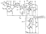
제1도는 본 발명의 1실시예를 도시한 반도체 메모리 장치의 고속입력 버퍼회로의 구성도이다.1 is a configuration diagram of a high speed input buffer circuit of a semiconductor memory device showing one embodiment of the present invention.
입력단자(301)에 입력된 ECL 레벨의 신호는 바이폴라 트랜지스터(302)에 의해 레벨 시프트되어 전류 절환형 회로의 바이폴라 트랜지스터(303)의 베이스에 유도된다. 이 커렌트 스위치 회로에 의해 입력 신호는 약 2V까지 증폭된다. 이때, 증폭전압이 너무 크게되거나, 입력단자의 전압이 -0.5V 이상으로 올라가거나 하면, 커렌트 스위치 회로의 바이폴라 트랜지스터(303)이 포화하고, 때로는 레치업 현상을 일으켜 메모리동작을 불가능하게 하는 일이 있다. 이것을 방지하기 위하여 바이폴라 트랜지스터(304)가 접속되어 있다.The signal of the ECL level input to the
이 바이폴라 트랜지스터(304)를 부가하는 것에 의해 입력 신호 전압이 규격값 이상으로 상승하거나, 전류절환형 회로의 출력진폭이 크게 되었을 때에도 트랜지스터(303)의 포화는 방지되어 회로의 안정한 동작을 얻을 수 있다. 전류 절환형 회로에 의해 증폭된 긍정과 부정의 신호는 MOS 트랜지스터(321), (331)을 부하로 하는 에미터 플로워 회로에 유도된다. 부하 MOS 트랜지스터(321), (331)의 소오스는 전원 VE1에 접속된다. 이 에미터 플로워 회로는 전류 절환형 회로의 부하를 가볍게 하고, 또한 후단의 회로를 높은 구동능력으로 구동하기 위하여 마련되고 있다. 여기에서 MOS 트랜지스터를 부하로서 사용한 것은 에미터 플로워 회로의 출력 진폭이 약 2V로 크기 때문에 부하로서 순수한 저항을 사용할 때에 비해서 저소비전력으로, 또한 고속 동작이 얻어지는 것에 기인하고 있다. 또 에미터 플로워 부하 저항과 MOSFET(321)을 병렬로 마련하는 것도 가능하다. 에미터 플로워 회로의 부정신호 출력은 MOS 트랜지스터(306)과 (307)의 게이트에, 긍정신호 출력은 MOS 트랜지스터(308)과 (309)의 게이트에 각각 유도되어 이 승압 회로에 의해 신호 진폭이 전원 전압까지 증폭된다. 이때, MOS 트랜지스터(310)은 출력의 전압이 접지 전위에 가까울 때에만 도통하고, 전원의 전위 VEE에 가까이 가면 그 도통은 없어져서 바이폴라 트랜지스터의 구동능력도 없게 된다. 즉, 이 회로는 출력이 고전위에서 저전위로 전환될 때에만 구동능력을 발휘하고, 그 이회일 때에는 구동능력이 없다는 것을 알 수 있다.The addition of this
또, 이 회로는 신호의 절환시 이외일 때에는 소비전력이 없어 저소비전력으로 동작하는 것은 물론이다. 이 회로의 후단에 부가된 MOS 트랜지스터(311)과 (312)는 신호의 절환시 이외에 있어서 이 회로에 구동능력을 갖게하고, 출력전위를 안정시키기 위하여 마련한 회로이다. MOS 트랜지스터(311)과 (312)의 게이트단자는 상술의 회로에서 입력 신호의 긍정과 부정을 교체한 회로(315)에서의 신호를 사용하고 있다. 이 때문에 이 MOS 트랜지스터의 게이트로의 신호는 이 회로의 절환 후에 도달하므로, 나머지 MOS 트랜지스터의 구동능력이 크면 지연시간을 증가하는 일도 있다. 통상, 양자의 구동능력의 비는 10:1 이상이 바람직하다. 이 회로에 의해 제4도에 도시한 값과 같은 기준으로 설계되었을 때, 입력버퍼의 지연시간은 2ns로 약 1ns 단축된다.In addition, this circuit has no power consumption when the signal is switched other than that, and of course, the circuit operates at low power consumption. The
제2도는 본 발명의 1실시예를 도시한 반도체 메모리 장치의 고속 디코더 회로의 구성도이다. 또, 제1도에 도시한 입력버퍼 회로에 의해 전원 전압까지 증폭된 입력 신호는 디코더 회로의 입력단자 a0에서 a7에 각각 공급된다. 이때, 입력 신호중 적어도 1개에 저레벨의 신호가 있으면, 이 디코더 회로는 저레벨을 출력한다. 즉, 각 입력을 게이트로하는 MOS 트랜지스터를 직렬로 접속하고 있기 때문에 1개라도 저레벨의 입력이 있으면 비도통으로 되어 출력은 저레벨로 된다. 이 회로에서는 입력의 신호 레벨에 의해 1개만 고레벨을 출력한다. 여기서 MOS 트랜지스터(410), (411)의 게이트에는 각 어드레스 신호의 부정신호![]()
![]()
![]()
![]()
제5도는 제2도의 디코더 회로의 입력, 노드(420), 출력(430)의 시간변화를 도시한 특성도이다. 신호입력에서 디코드 신호가 만들어지는 노드(420)까지 약 0.5ns, 전원 전압까지의 승압에 약 1ns의 합계 1.5ns에서 디코드하고 있다.5 is a characteristic diagram illustrating time variation of the input, node 420, and
본 실시예에서는 N찬넬 MOS 트랜지스터에 대해서 기술하고 있지만, 물론 P찬넬 MOS 트랜지스터를 사용하여도 좋다. 또, 긍정, 부정 신호를 사용하지 않고 N찬넬, P찬넬 MOS 트랜지스터를 상보형에 사용하고 한쪽의 신호만으로 디코드하는 것도 가능하다.In this embodiment, the N channel MOS transistor is described, but of course, a P channel MOS transistor may be used. It is also possible to use N-channel and P-channel MOS transistors in the complementary type and decode with only one signal without using a positive or negative signal.
제6도는 제2도의 변형예를 도시한 디코더 회로의 구성도이다. 제2도에서는 모든 어드레스 신호가 고레벨일 때에만 출력이 고레벨로 되는 디코더 회로를 도시했지만, 제6도에 도시한 것과 같이 모든 어드레스신호가 고레벨일 때에만 출력이 저레벨로 되는 회로로 할 수도 있다. 동작은 제2도와 거의 같기 때문에 설명을 생략한다.6 is a configuration diagram of a decoder circuit showing a modification of FIG. In FIG. 2, a decoder circuit in which the output becomes a high level only when all the address signals are at a high level is illustrated. However, as shown in FIG. 6, the output circuit can be made low in only when all the address signals are at a high level. Since the operation is almost the same as in FIG. 2, the description is omitted.
제7도는 제6도의 각 노드의 전압의 시간 변화를 도시한 특성도이다. 디코더 회로의 지연시간은 제2도의 회로의 지연시간과 거의 동일하다. 즉, 입력노드 a0에 0ns의 시점에 입력이 있으면 노드(721)에서 디코드되는데 약 0.5ns 걸리고, 출력노드(731)에서 전원 전압까지 승압되는데 약 1ns 걸리므로 합계 1.5ns 걸린다. 출력노드(731)에서는 역극성의 출력을 공급한다.FIG. 7 is a characteristic diagram showing the time variation of the voltage of each node in FIG. The delay time of the decoder circuit is almost equal to the delay time of the circuit of FIG. That is, if there is an input at the time of 0ns at the input node a0, it takes about 0.5ns to decode at the
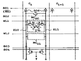
제8도는 본 발명의 1실시예를 도시한 메모리 셀의 구성도로서, 데이타선(810), (811)의 부하소자로서 쇼트키 장벽형 다이오드(806)을 사용하고 있다. 제8도에 있어서 선(801)은 라이트 인에이블 신호 WE와 역상인 신호![]()
![]()
메모리 셀 MC0으로의 데이타의 라이트를 할 때에는 데이타 라이트선(803), (804)에 접속된 데이타 라이트 회로(도시하지 않음)에서 Y스위치 Q6, Q7, 데이타선(810), (81l)을 거쳐서 데이타가 메모리 셀 MC0에 전달된다. 이때, 선(801)은 부전원 전압 VEE에 바이어스되기 때문에 1쌍의 쇼트키 장벽 다이오드(806)의 임피던스는 크게되어 라이트 데이타가 데이타선 부하소자를 거쳐서 선(801)에 리이크하는 것을 방지한다.When writing data to the memory cell MC 0 , the Y switches Q 6 , Q 7 ,
출원전은 이 데이타선 부하 저항으로서 MOS 트랜지스터가 사용되고 있으며, 최근에는 바이폴라 트랜지스터를 사용하는 시도도 보고되고 있다. 전자의 MOS 트랜지스터를 사용한 경우에는 고속화를 위해 저항값을 내리려고하면 MOS 트랜지스터의 게이트폭을 크게할 필요가 있으며, 예를 들면 실효 저항값 500Ω을 얻기 위해서는 게이트폭을 40㎛ 이상으로 설계하는 것이 필요하게 된다. 이 결과, 데이타선 쌍당의 MOS 트랜지스터의 게이트 용량은 100fF에 달하고, 메모리 정보의 라이트시에 이 MOS 트랜지스터의 약 60개를 전부 비도통으로 하기 위해서는 6pF 정도 큰 정전용량을 구동하는 구동 회로가 필요하게 된다. 또, 메모리 정보를 라이트할 때에 전원전압 VEE까지 인하된 데이타선은 이 MOS 트랜지스터에 의해 접지 전위까지 연상되어 계속 정보의 리드에 대비하게 되지만, 통상, 이 데이타선(810), (811)에는 1pF 정도의 정전용량이 부가되어 있기 때문에 500Ω의 실효 저항으로 인상하면 그 때 정수는 0.5ns로 되어 정보 리드시의 데이타선의 진폭이 50mV까지 도달하기에는 3ns나 걸린다. 즉, 이 동안에 정보의 리드가 개시되면, 데이타선의 진폭이 50mV에 도달할 때까지의 시간만큼 리드시간이 증폭한다. 이 결점을 회피하기 위하여 데이타선의 부하소자로서 바이폴라 트랜지스터를 사용하는 것이 제안되고 있다. 바이폴라 트랜지스터를 사용하면, 라이트시의 데이타선 부하를 비도통으로 하는 것도 또, 라이트 후의 데이타선의 전위 인상에도 고속화를 기대할 수 있다. 그러나, 바이폴라 트랜지스터의 에미터·베이스 접합의 항복전압이 낮고, 특히 고속으로 동작하는 바이폴라 트랜지스터에서는 그 항복전압은 3V 정도로 그치고 있으며, 베이스 단자 전압을 -5V의 부전원전압 VEE까지 인하해서 그 바이폴라 트랜지스터를 비도통으로 하는 것은 곤란하다.Prior to the application, a MOS transistor is used as this data line load resistor, and in recent years, an attempt to use a bipolar transistor has also been reported. In the case where the former MOS transistor is used, the gate width of the MOS transistor needs to be increased in order to reduce the resistance value for high speed. For example, in order to obtain an effective resistance value of 500 mA, the gate width must be designed to be 40 μm or more. Done. As a result, the gate capacity of the MOS transistors per pair of data lines reaches 100fF, and in order to make all 60 of these MOS transistors non-conductive when the memory information is written, a driving circuit for driving a capacitance of about 6pF is required. . When writing memory information, the data line lowered to the power supply voltage V EE is associated with the ground potential by this MOS transistor, and continues to prepare for the read of the information. Since a capacitance of about 1 pF is added, when it is raised to an effective resistance of 500 mA, the constant becomes 0.5 ns, and it takes 3 ns for the amplitude of the data line to reach 50 mV at the time of information read. That is, when reading of information is started during this time, the read time is amplified by the time until the amplitude of the data line reaches 50 mV. In order to avoid this drawback, it is proposed to use a bipolar transistor as a load element of a data line. By using a bipolar transistor, non-conduction of the data line load at the time of writing can also be expected to increase the speed even when the potential of the data line after writing is increased. However, the breakdown voltage of the emitter-base junction of the bipolar transistor is low, especially in the bipolar transistor operating at high speed, the breakdown voltage is only about 3V, and the base terminal voltage is lowered to the negative power supply voltage V EE of -5V so that the bipolar transistor It is difficult to make a transistor non-conductive.
이것에 대해서, 본 실시예와 같은 쇼트키 장벽형 다이오드를 사용하면, 이러한 쇼트키 장벽형 다이오드는 반도체 집적 회로에 있어서는 바이폴라 트랜지스터의 저불순물 농도의 콜렉터 영역을 금속과의 정류성 접촉에 의해 구성되기 때문에 항복전압도 비교적 크게된다. 따라서, 바이폴라 트랜지스터를 사용하였을 때와 동등한 고속성을 얻을 수 있는 것과 함께 그 비도통으로 하기 위한 다이오드의 양극 단자의 음극에 대한 정전용량은 10fF 이하이며, 그 제어도 간단하게 행할 수가 있다.On the other hand, using the same Schottky barrier type diode as in the present embodiment, such a Schottky barrier type diode is constituted by rectifying contact with a metal in a collector region of low impurity concentration of a bipolar transistor in a semiconductor integrated circuit. Therefore, the breakdown voltage is also relatively large. Therefore, the same high speed as in the case of using a bipolar transistor can be obtained, and the capacitance of the anode terminal of the diode for non-conduction is 10 fF or less, and the control can be easily performed.
제9도는 제8도의 회로를 사용하였을 때의 데이타선의 전위가 전원전압 VEE로부터 회복하는 시간 변화를 도시한 특성도이다. 데이타선쌍의 전위차가 50mV로 되는데 요하는 시간은 약 1.2ns이며, 이것은 종래의 MOS 트랜지스터를 사용했을 때에 비해서 1.8ns나 고속화되어 있다.FIG. 9 is a characteristic diagram showing the time change when the potential of the data line recovers from the power supply voltage V EE when the circuit of FIG. 8 is used. The time required for the potential difference of the data line pair to be 50 mV is about 1.2 ns, which is 1.8 ns faster than that of the conventional MOS transistor.
제10도는 제2도의 변형예를 도시한 메모리 셀의 구성도이다. 제8도의 N찬넬 MOSFET Q5는 제10도에 있어서는 P찬넬 MOSFET Q'5로 치환되고, 또 다른 P찬넬 MOSFET Q9, Q10과 그 이외의 쇼트키 장벽형 다이오드 D3, 전류원 CS가 추가적으로 배치되어 있다.FIG. 10 is a configuration diagram of a memory cell showing a modification of FIG. N channel MOSFET Q 5 in FIG. 8 is replaced by P channel MOSFET Q ' 5 in FIG. 10, and another P channel MOSFET Q 9 , Q 10 and other Schottky barrier diodes D 3 and current source CS are additionally added. It is arranged.
제8도의 실시예에 있어서는 선(801)의![]()
![]()
이것에 대해서 제10도의 실시예에 있어서는 P찬넬I MOSFET Q'5, Q9, Q10의 게이트는 선(803)의 라이트 인에이볼 신호 WE에 의해 제어되어 있으므로 라이트 상태를 제거한 동작상태에 있어서는 이들의 MOSFET Q'5, Q9, Q10은 도통상태로 된다. 따라서, 선(801)의![]()
![]()
![]()
![]()
다음에 본 발명에 있어서의 입력버퍼 회로의 다른 실시예에 대해서 설명한다.Next, another embodiment of the input buffer circuit according to the present invention will be described.
제11도는 본 발명의 다른 실시예를 도시한 입력버퍼 회로의 구성도로서, 에미터 플로워 회로의 최소회로 구성을 도시한다. 제11도에 있어서 (1)은 입력단자, (2)는 출력단자, (3)은 기준전압 인가단자, (4)는 부전원단자, (100)은 NPN 바이폴라 트랜지스터, (101)은 P찬넬형 MOS 트랜지스터(이하, PMOS라고 칭한다)를 도시하고 있다. 본 실시예에 의한 에미터 플로워 회로로 구성된 입력버퍼는 제13도에 도시한 것과 같이 적어도 1개의 바이폴라 트랜지스터와 PMOS에 의해 구성된다. 입력전압이 고레벨, 예를 들면 접지전위인 경우에는 NPN 트랜지스터(100)의 에미터 단자(2)에 그의 베이스·에미터 사이의 전압 VBE, 예를 들면 0.8V의 낮은 전압이 출력된다. 이때, PMOS(101)이 도통하여 소정의 에미터 바이어스 전류 IEH가 흐르도록 PMOS(101)의 게이트 전압, 즉 단자(3)의 전위를 설정한다. 다음에 입력 전압이 저레벨, 예를 들면 -0.8V인 경우에는 상기와 마찬가지로 해서 출력단자(2)에는 베이스·에미터 사이의 전압만큼 낮은 전압이 출력된다. 그러나, 이 때에는 PMOS(101)의 소오스 전위, 즉 출력단자(2)의 전위는 상기 입력 전압이 고레벨인 경우에 비해서 입력 신호 진폭만큼 내려가기 때문에 PMOS(101)의 게이트·소오스 사이의 전압VGS는 감소하고, 에미터 바이어스 전류 IEL도 감소한다.11 is a configuration diagram of an input buffer circuit showing another embodiment of the present invention, showing the minimum circuit configuration of the emitter follower circuit. In Fig. 11, (1) is an input terminal, (2) is an output terminal, (3) is a reference voltage applying terminal, (4) is a negative power supply terminal, (100) is an NPN bipolar transistor, and (101) is a P channel. A type MOS transistor (hereinafter referred to as PMOS) is shown. The input buffer composed of the emitter follower circuit according to the present embodiment is constituted by at least one bipolar transistor and a PMOS as shown in FIG. When the input voltage is at a high level, for example, a ground potential, the voltage V BE between its base and emitter, for example, a low voltage of 0.8 V, is output to the
제12도는 제l1도에 있어서의 입력전압 대 에미터 전류 특성의 일예를 도시한 도면이다. PMOS 대신에 저항을 사용한 경우에는, 예를 들면 전원전압 -5.2V, 에미터·베이스 사이의 전압 0.8V로 하고, 입력전압 고레벨 0V, 저레벨 -0.8V로 하면, 입력전압 고레벨 0V, 저레벨 -0.8V에 대해서 에미터 전류는(IEH-IEL)/IEH=0.8/(5.2-0.8)=18%밖에 변화하지 않는데 대하여, 본 실시예에 의한 회로에서는 상술과 같이 PMOS(101)의 게이트(3)의 설정전위에 의해 입력전압이 고레벨, 저레벨시의 에미터 전류비를 임의로 설정하는 것이 가능하게 되어 회로의 저소비전력화가 도모된다. 또, NPN 트랜지스터(100) 대신에 N찬넬형 MOS 트랜지스터(이하 NMOS라고 칭한다)를 사용하는 것에 의해 유사한 효과를 발휘하는 소오스 플로워 회로를 실현할 수가 있다.FIG. 12 is a diagram showing an example of input voltage versus emitter current characteristics in FIG. When a resistor is used instead of the PMOS, for example, the voltage between the power supply voltage -5.2V and the emitter-base is 0.8V, and the input voltage high level 0V and the low level -0.8V are set. The input voltage high level 0V and the low level -0.8 The emitter current changes with respect to V only (I EH -I EL ) / I EH = 0.8 / (5.2-0.8) = 18%. In the circuit according to the present embodiment, the gate of the
제13도는 본 발명의 다른 실시예를 도시한 에미터 플로워 회로로 되는 입력 버퍼의 구성도이다. 제13도에서는 입력단자(11), 출력단자(12), 기준전압 인가단자(13), 전원단자(14), NPN 트랜지스터(110), PMOS(111) 이외에 PMOS(111)과 전원단자(14) 사이에 NMOS(112)를 부가하여 출력단자(12)와는 신호레벨이 다른 출력 신호를 단자(15)에서 끄집어내도록 한다. 이렇게하면 CMOS 회로에 있어서의 PMOS, NMOS 각각의 입력 신호에 적합한 2종류의 출력 신호를 얻을 수가 있다. 즉, 본 실시예의 회로에서는 제11도의 실시예에 있어서 에미터 플로워 회로의 전류 변화를 (112), (114)로 구성되는 커렌트 미러 회로에서 검출하는 점에 특징이 있다. 단자(11)의 입력 신호를, 예를 들면 고레벨 0V, 저레벨 -0.8V, 베이스·에미터 사이의 바이어스 전압을 0.8V로 하면, 출력단자(12)에는 제11도의 실시예와 마찬가지로 고레벨 -0.8V, 저레벨 -1.6V의 출력 신호가 얻어진다. 이 신호는 접지 레벨에 가까운 신호이며 다음단의 CMOS 회로에 있어서의 PMOS의 입력 신호에 적합한 신호이다. 이것에 대해서 CMOS 회로에 있어서 NMOS의 입력 신호로서는 전원단자(14)에 인가한 전압에 가까운 레벨의 출력 신호가 필요하다. 제13도에서는 NPN 트랜지스터(110), PMOS(111)은 제12도의 실시예와 마찬가지로 동작하여 NMOS(112)의 작용에 의해 상술의 NMOS의 입력 신호에 적합한 출력 신호를 단자(15)에서 얻을 수가 있다. 입력 신호가 저레벨일 때 PMOS(111)은 약간 도통한 상태로 되고, 에미터 전류는 약간 흐르는 정도로서 이 전류에 대응한 NMOS(112)의 게이트 전위, 즉 출력단자(15)의 전위는 NMOS(112)의 임계 전압, 또는 그것보다도 조금 높은 전압만큼 전원전압보다 높은 값으로 된다. 입력 신호가 고레벨일 때에는 PMOS(111)은 도통하여 에미터 바이어스 전류가 흐르는 것과 동시에 이 전류에 대응해서 NMOS(112)의 게이트 전위는 상승하여 NMOS의 임계 전압보다도 매우 큰 값으로 된다.13 is a configuration diagram of an input buffer including an emitter follower circuit showing another embodiment of the present invention. In FIG. 13, the
따라서, 제13도의 에미터 플로워 회로에서는 CMOS 구성의 회로를 구동하기 위하여 적합한 2종류의 출력 신호를 동시에 얻을 수가 있어 에미터 플로워 회로와 카렌트 미러 회로를 독립으로 구성한 경우에 비해서 회로의 간략화, 고성능화가 도모된다.Therefore, in the emitter follower circuit of FIG. 13, two types of output signals suitable for driving a circuit having a CMOS configuration can be obtained simultaneously, which simplifies and improves the circuit performance as compared with the case where the emitter follower and the current mirror circuit are independently configured. Is promoted.
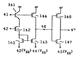
제14도는 본 발명의 또 다른 실시예를 도시한 에미터 플로워 회로를 사용한 입력버퍼의 구성도이다. 제14도에 있어서, (21), (24)는 상보적인 신호를 입력하는 단자,(22), (25)는 상보적인 신호를 출력하는 단자, (23), (26)은 전원단자, (120), (122)는 NPN 트랜지스터, (121), (123)은 PMOS, (124), (125)는 저항이다. 이 회로에서는, 예를 들면 전류 절환형 회로의 출력 신호와 같은 상보관계에 있는 신호를 입력단자(21), (24)에 인가하고, 그 출력 신호를 출력단자(22), (25)를 거쳐서 각각 PMOS(123), (121)에 부여하여 이들을 도통, 또는 비도통으로 하는 것에 의해 저소비전력화를 도모하고 있다. 단자(21)의 입력 신호가 고레벨, 예를 들면 0V, 단자(24)의 입력신호 레벨이 저레벨 예를 믈면 -1.5V로 하면, 출력단자(22), (25)에는 각각 -0.8V, -2.3V의 전압이 나타난다. 따라서, PMOS(121), (123)의 게이트 소오스 사이의 전압 VGS는 각각 -1.5V, 1.5V이고, 임계 전압이 예를 들면 -0.6V이면, PMOS(121)은 도통하고 PMOS(123)은 비도통으로 된다. 입력 신호가 역의 경우도 마찬가지로서 PMOS(121)은 비도통, PMOS(123)은 도통으로 된다. 저항(124), (125)는 약간의 바이어스 전류를 흐르게 하기 위한 것이다. 따라서, 본 실시예의 에미터 플로워 회로에서는 제11도의 단자(3)에 인가하는 기준전압을 인가하는 일없이 회로의 저소비전력화를 도모할 수 있다.14 is a configuration diagram of an input buffer using an emitter follower circuit showing still another embodiment of the present invention. In Fig. 14,
제15도는 본 발명의 다른 실시예를 도시한 입력 버퍼 회로의 구성도이다. 제15도에 있어서, (31)은 신호입력단자, (32)는 기준전압 인가단자, (33)∼(35)는 VCC의 정전원단자, (36), (37)은 출력단자, (130)은 PNP 트랜지스터, (139), (140)은 NPN 트랜지스터, (131), (133), (135), (136), (137)은 NMOS, (132), (l34), (138)은 PMOS이다. 이 회로에서는 TTL 레벨 신호와 같은 접지 전위에 가까운 비교적 작은 진폭의 신호를 전원 전압에 가까운 진폭의 신호로 증폭하고, 또 이것을 MOS 트랜지스터와 바이폴라 트랜지스터로 되는 버퍼회로에 입력하여 부하를 구동한다. 본 실시예에 있어서, PNP 트랜지스터(130), NMOS(131), PMOS(132)는 제13도의 실시예에 있어서 NPN 트랜지스터(110), PMOS(111), NMOS(112)와 유사한 동작을 행한다. 즉, 입력 신호(31)의 고저에 의해 NMOS(131)은 비도통, 도통으로 되어 그 드레인 전극에는 PMOS(134)의 입력에 적합한 전원 전압에 가까운 고·저의 신호가 얻어진다. 한편, NMOS(133)에는 입력신호를 인가하는 것에 의해 입력 신호가 고레벨일 때에는 NMOS(133)은 도통, PMOS(134)는 비도통으로 되어 이 레벨 변환 회로의 출력단자(36)은 접지 전위에 가까운 저레벨로 된다. 입력 신호가 저레벨일 때에는 NMOS(133)은 비도통, PMOS(134)는 도통하여 출력단자(36)은 전원전압에 가까운 고레벨로 된다. 본 실시예에서는 이 레벨 변환 후의 신호를 바이폴라 트랜지스터와 MOS 트랜지스터(135)∼(140)으로 구성되는 버퍼 회로에 인가되어 출력단자(37)에 접속된 부하를 구동하는 것에 의해 이 레벨 변환 회로의 구동능력을 증가시켜 고속 성능을 실현하고 있다.15 is a configuration diagram of an input buffer circuit showing another embodiment of the present invention. In Fig. 15,
NMOS(133) 또는 PMOS(134)에 인가하는 신호의 진폭은 비교적 작기 때문에 큰 부하를 구동하기에는 적합하지 않으며, 따라서 상기 버퍼 회로를 삽입해서 출력단자(36)에 접속되는 부하를 경감한쪽이 고속이었다. 버퍼 회로로서는 CMOS 인버터 회로, 다입력 논리 게이트 회로이어도 지장은 없다. PNP 트랜지스터로서는 세로형의 것을 사용할 수 없으면 가로형의 것이어도 지장은 없다. 또, PMOS를 사용하여 소오스 플로워 회로를 구성하는 것도 가능하다. 또 본 실시예에 있어서는 TTL 레벨(저레벨 0.8V, 고레벨 2.2V)의 입력을 상정해서 NMOS(l33)의 게이트 전극을 입력단자(31)에 접속하고 있지만 입력 신호 레벨에 의해서는 제15도의 실시예와 마찬가지로 해서 PNP 트랜지스터(130)의 에미터 단자에 접속해도 좋다. 이와 같이 본 실시예에 의한 회로에서는 TTL 레벨 입력 신호를 CMOS 회로 등에 적합한 신호로 고속으로 변환할 수가 있어 LSI의 입력부에서의 신호 지연을 저감할 수가 있다.Since the amplitude of the signal applied to the
제16도는 본 발명의 또 다른 실시예를 도시한 입력 버퍼 회로의 구성도이다. 제16도에 있어서,(41)은 신호 입력단자, (42)는 기준전압 인가단자, (43)∼(45)는 VEE전원단자, (46)∼(47)은 출력단자, (141)은 NPN 트랜지스터, (143), (145), (147)은 NMOS, (142), (144), (146)은 PMOS이다. 이 회로에서는 ECL 레벨 신호와 같은 접지 전위에 가까운 작은 진폭의 신호를 VEE전원 전압에 가까운 진폭의 신호로 증폭하고, 또 이것은 CMOS 구성의 버퍼 회로에 입력하여 부하를 구동하고 있다. 본 실시예에 있어서의 NPN 트랜지스터(141), PMOS(142), NMOS(143), 또 PMOS(144), NMOS(l45)는 각각 제15도의 실시예에 있어서의 PNP 트랜지스터(130), NMOS(131), PMOS(132), 또 NMOS(133), PMOS(134)와 같은 동작을 행하고, 출력단자(46)에는 입력 신호의 고저에 따라서 전원 전압에 가까운 진폭의 저레벨, 고레벨의 신호가 얻어진다. PMOS(146), NMOS(147)에 의한 CMOS 인버터 회로는 이 신호를 받아서 제15도의 실시예의 (135)∼(140)으로 되는 인버터 회로와 같은 부하를 고속으로 구동할 수가 있다. 본 실시예의 또 다른 특질은 사용하는 바이폴라 트랜지스터가 콜렉터 접지의 NPN 트랜지스터(141)뿐이며 통상의 CMOS 공정으로 실현할 수 있는 점에 있다.16 is a configuration diagram of an input buffer circuit showing another embodiment of the present invention. In Fig. 16,
제17도는 본 발명의 또 다른 실시예를 도시한 입력 버퍼 회로의 구성도이다. 제17도에 있어서, (51)은 신호 입력단자, (52)∼(54), (59)는 기준전압 인가단자, (63)∼(69)는 VEE전원단자, (55)∼(58), (60)은 내부신호단자, (61), (62)는 출력단자, (200)은 버퍼 회로, (201)은 회로(200)과 동일한 회로, (150), (154), (155), (157), (166), (167)은 NPN 트랜지스터, (156), (159), (16l), (163), (164), (165)는 NMOS, (151), (158), (160), (162)는 PMOS, (152), (153)은 저항이다. 이 회로에서는 ECL 레벨의 입력 신호를 (152)∼(156)으로 구성되는 전류 절환형 회로로 증폭한 후, 회로(200), 또는 (20l)로 전원 전압에 가까운 진폭으로 레벨 변환해서 부하를 고속으로 구동하고 있다. NPN 트랜지스터(150), PMOS(151)에 의해 구성되는 회로는 입력 신호를 후단의 전류 절환형 회로에 적합한 레벨로 시프트하는 회로이며, 그 동작은 제13도에서 기술한대로이다. 전류 절환형 회로의 출력 진폭의 설정에 의해서는 NPN 트랜지스터(154), (155)가 포화하는 것을 방지하기 위하여 NPN 트랜지스터(150)의 에미터와 (154)의 베이스 사이에 다이오드 또는 자항을 삽입하고, 또 레벨 시프트하는 것도 가능하다. 구성 소자(152)∼(156)으로 구성되는 회로는 전류 절환형 회로이며, 기준전압 인가단자(54)의 전위를 NPN 트랜지스터(154)의 베이스 신호의 사이에 할당되는 것에 의해 그 출력단자(55), (56)에는 각각 입력 신호의 부정, 긍정 신호가 출력된다. 이 신호는 제18도에서 기술한 경우와 같은 레벨 변환 및 버퍼 회로(200), 또는 (201)에 의해 증폭된다. 그 입력 신호 진폭은 버퍼 회로(200) 또는 (201)의 입력 신호로서는 클수록 좋지만, 너무 크면 전류 절환형 회로부에서의 지연이 증가한다. 실험에 있어서는 단자(55), (56)에서의 신호 진폭은 약 1.3V가 전체의 지연시간을 최소로 할 수가 있어 가장 적합하다.17 is a block diagram of an input buffer circuit showing another embodiment of the present invention. In Fig. 17,
또, 본 실시예에 있어서의 전류 절환형 회로에서는 NMOS(156)을 사용하고 있다. 이것은 저전원 전압에 있어서도 이 회로를 동작 가능하게 하기 위한 것이며, 기준전압 인가단자(53)에 적절한 전압을 인가하여 NMOS(156)을 포화 영역에서 동작시키는 것에 의해 거의 일정한 바이어스 전류를 공급할 수가 있어, 단자(55), (56)의 출력 진폭을 거의 일정하게 할 수가 있다. 레벨 변환 및 버퍼 회로(200), (201)은 제16도의 실시예와 마찬가지인 회로이다. 그 입력 신호(55), (56)의 고레벨이 접지 전위이기 때문에 트랜지스터(157)에 의해 이 접지 전위를 -0.8V 레벨 시프트한 신호를 PMOS(160)의 게이트 입력 신호로 해도 NMOS(161)이 도통시에 PMOS(160)은 약간 도통하는 것 뿐이므로 그 기능을 다할 수가 있다. 이 트랜지스터(157)의 베이스 전극에서 PMOS(160)의 게이트 신호를 얻는 목적은 트랜지스터(157)의 베이스 전극에서 상기 신호를 얻는 경우에 비해서 저레벨이 0.8V 내려가고, PMOS(160)의 부하 구동능력이 그만큼 증가하여 지연 시간을 저감할 수 있는데 있다. 물론 경우에 따라서는 제16도의 실시예와 같은 접속으로 해도 지장은 없다. 또, 제21도의 버퍼 회로(200), (201)에서는 제16도의 CMOS 인버터 회로 대신에 보다 고속적인 제15도의 실시예에 도시한 바이폴라 CMOS 구성의 인버터 회로를 사용해서 고속 동작을 실현하고 있다.In the current switching circuit in this embodiment, the
제l8도는 제17도의 회로의 동작 파형을 도시한 도면이다. 제17도의 단자(61), (62)에 접속되는 부하 용량은 1pF이다. 제18도에는 입력단자(51)의 파형(파선), 출력단자(55), (56)의 파형, 버퍼 회로의 중간단자(57), (58), (60)의 파형 및 부하 출력단자(61), (62)의 파형이 도시되어 있다.FIG. 18 is a diagram showing an operating waveform of the circuit of FIG. The load capacitance connected to the
이와 같이 본 실시예에 의한 회로에서는 ECL 입력(고레벨 -0.9V, 저레벨 -1.7V)에 대해서 단자(61), (62)에 각각 그 부정, 긍정 출력을 지연시간 2.3ns에서 얻을 수가 있다. 또, 이 때의 소비전력은 대기시 7mW, 사이클 시간 10ns 동작시 11mW와 저소비전력에서 고속으로 동작할 수가 있다.As described above, in the circuit according to the present embodiment, the negative and positive outputs of the
즉, 본 실시예에 있어서는 종래에는 거의 일정한 정상 전류를 흘리고 있던 에미터 플로워 회로의 바이어스 전류를 그 입력 신호의 고·저에 의해 변화시키므로 고속 성능을 손상시키는 일없이 소비전력을 저감할 수가 있다. 또 이 바이어스 전류를 변화시키는 것을 이용해서 ECL 또는 TTL 레벨의 신호를 CMOS 회로등에 적합한 레벨의 신호로 고속으로 변환할 수가 있으므로 집적 회로의 고성능화에 기여할 수 있다.In other words, in the present embodiment, since the bias current of the emitter follower circuit, which has conventionally flowed a substantially constant steady current, is changed by high and low of the input signal, power consumption can be reduced without compromising high-speed performance. By changing the bias current, a signal of an ECL or TTL level can be converted into a signal of a level suitable for a CMOS circuit or the like at high speed, thereby contributing to the improvement of the integrated circuit.
제19도는 입력 버퍼 회로(200), 바이폴라 논리 디코더 회로(202), 레벨 변환 회로(203)으로 되는 본 발명의 반도체 집적 회로 장치의 1실시예로서 2비트의 디코더 회로를 도시한 것이다. 이 회로도에 따라서 본 발명의 반도체 집적 회로 장치의 구성, 동작을 설명한다.FIG. 19 shows a 2-bit decoder circuit as one embodiment of the semiconductor integrated circuit device of the present invention, which is an
제19도에 있어서, (200)은 입력 버퍼 회로, (201)은 회로(200)과 동일한 입력 버퍼 회로, (202)는 와이어드 논리합 디코더 회로, (203)은 레벨 변환 회로, (204)∼(206)은 회로(203)과 동일한 레벨 변환 회로, (1), (2)는 입력단자, (3)∼(7)은 기준잔압 인가단자, (8)∼(14)는 전원단자, (15)∼(22)는 내부 신호단자, (23)∼(26)은 상기 회로블럭의 출력단자, 소자(100)∼(105)는 NPN 바이폴라 트랜지스터(이하 NPN 트랜지스터라고 액칭한다), 소자(106)∼(109)는 멀티에미터형의 NPN 바이폴라 트랜지스터(이하 NPN 트랜지스터라고 약칭한다), 소자(110) ∼(112)는 저항, 소자(113)∼(121)은 N찬넬형 MOSFET(이하 NMOS라고 약칭한다), 소자(122), (123)은 P찬넬형 MOSFET(이하 PMOS라고 약칭한다)를 도시하고 있다.In Fig. 19,
종래의 장치, 예를 들면(ISSCC DIGEST OF TECHNICAL PAPERS, (1986년) pp212∼213)에 있어서 거론되고 있는 고속적인 레벨 변환 회로에서는 상보적인 2개의 입력 신호가 필요하기 때문에 MOS계 내부회로의 신호에 적합한 신호 레벨로의 변환은 상기 상보 신호가 존재하는 입력 버퍼 출력의 단계에서 행하여지고 있었다.The high-speed level converting circuit discussed in the conventional apparatus, for example (ISSCC DIGEST OF TECHNICAL PAPERS, pp. 1212), requires two input signals complementary to the signal of the MOS internal circuit. Conversion to the appropriate signal level was done at the stage of the input buffer output where the complementary signal is present.
이것에 대하여 본 발명으로 되는 장치에서는 예를 들면 제19도의 실시예에 있어서 레벨 변환 회로(203)에 의해 상보 신호를 사용하지 않고 단일의 입력 신호(19)를 고속으로 레벨 변환하는 것이 가능하게 되므로 고속적인 바이폴라계의 논리 회로를 조립할 수가 있다. 이것에 의해 종래 MOS계의 내부 회로로 구성되어있던 회로 기능 블럭을 고속적인 바이폴라계의 회로로 치환하는 것이 가능하게 된다.On the other hand, in the apparatus according to the present invention, for example, in the embodiment of FIG. 19, it is possible to level convert a
다음에 제19도에 도시한 2비트 디코더 회로의 동작을 실명한다.Next, the operation of the 2-bit decoder circuit shown in FIG. 19 is lost.
제19도에 있어서, 회로(200), (201)은 입력 버퍼 회로이며, 단자(1) 또는 (2)에 입력되는 ECL(Emitter Coupled Logic) 레벨의 입력 신호를 검출, 증폭하여 각각 단자(15), (16) 또는 (17), (18)에 상보적인 2개신호를 출력한다.In FIG. 19, the
또, NPN 트랜지스터(100) 및 NMOS(113)에 의해 구성되는 회로는 소자(101)∼(103) 및 (110)∼(112)로 구성되는 전류 절환형 회로에 적합한 신호 레벨로 입력 신호를 레벨 시프트하는 회로이다. 즉, NMOS(113)의 게이트 단자(3)에 적절한 기준전압을 인가하고 NMOS(113)을 포화 영역에서 동작시키는 것에 의해 거의 일정한 바이어스 전류를 공급할 수가 있다.Further, the circuit constituted by the
물론 통상의 NPN 트랜지스터 저항에 의한 정전류 회로 구성으로 해도 좋지만, 상기한 방법이 회로 구성이 간단하며 저전원 전압 동작이 가능하다.Of course, a constant current circuit configuration using a conventional NPN transistor resistor may be used. However, the above-described method is simple in circuit configuration and low-power voltage operation is possible.
또, 전류 절환형 회로의 출력 진폭의 설정에 의해서는 NPN 트랜지스터(101), (102)가 포화하는 것을 방지하기 위하여 NPN 트랜지스터(100)의 에미터와 NMOS(113)의 드레인 사이에 다이오드, 또는 저항과 용량 소자를 삽입하고, 또 레벨 시프트하는 것도 가능하다.Also, by setting the output amplitude of the current switching circuit, the diode between the emitter of the
다음에 전류 절환형 회로는 단자(5)의 전위를 NPN 트랜지스터(101) 의 베이스 신호의 고·저레벨의 사이에 할당되는 것에 의해 그 출력단자(15), (16)에 각각 입력 선호의 부정, 긍정 신호를 출력하도록 동작한다.Next, in the current switching circuit, the potential of the
또, NPN 트랜지스터(103), 저항(112)에 의한 회로는 정전류원 회로이며, 전류값의 정밀도를 필요로 하지 않는 경우에는 상술과 마찬가지로 NMOS만으로 구성해도 좋다.In addition, the circuit by the
상기의 전류 절환형 회로의 출력 신호 진폭은 후단의 레벨 변환 회로의 입력 신호 진폭을 고려하면 클수록 좋지만, 너무 크게하면 전류 절환형 회로부에서의 지연시간이 증대한다. 또 NPN 트랜지스터(101) 및 (102)가 포화하지 않도록 설계하지 않으면 안된다. 실험에서는 상기 출력 신호로서는 약 1.4V가 가장 적합하였다.The output signal amplitude of the current switching circuit is better in consideration of the input signal amplitude of the subsequent level conversion circuit, but if it is too large, the delay time in the current switching circuit portion increases. In addition, the
다음에 디코더 회로(202)는 와이어드 논리합 회로이며, 그 출력단자(단자(19), (20), (21), (22))에 접속된 멀티에미터형의 NPN 트랜지스터의 베이스 전위가 1개라도 고레벨이면 출력단자에 고레벨을 출력하고, 상기 베이스 전위가 모두 저레벨일 경우는 출력단자에 저레벨을 출력한다.Next, the
따라서, 제19도와 같이 입력 버퍼 회로의 긍정, 부정 신호를 입력으로 하여 동일 도면과 같이 결선하는 것에 의해 단자(19)∼(22)에는 단자(1), (2)의 입력 신호에 대한 디코드 신호(저레벨 선택)가 출력된다. 예를 들면 단자(1), (2) 모두 저레벨일 경우에는 단자(15), (17)은 고레벨, 단자(16), (18)은 저레벨로 되고, 따라서 단자(19)∼(21)은 고레벨, 단자(22)가 저레벨로 되어 선택된다.Therefore, as shown in FIG. 19, the positive and negative signals of the input buffer circuit are inputted and connected as shown in the same drawing to decode the signals for the input signals of the
또, NMOS(114)∼(117)은 NMOS(113)가 마찬가지로 에미터 플로워 회로에 바이어스 전류를 공급하기 위한 것이다.The
또한, 멀티에미터형의 NPN 트랜지스터(106)∼(109)는 단일 에미터형의 NPN 트랜지스터의 베이스와 콜렉터를 공통으로 하여 구성하여도 좋은 것은 물론이다.It is a matter of course that the multi-emitter
다음에 회로(203)∼(206)은 상기 디코드된 신호를 다음단의 MOS계의 내부 회로에 적합한 레벨의 신호로 레벨 변환하는 회로이다.Next, the
상기의 회로에 있어서, 예를 들면 입력 버퍼 회로(200)의 출력 진폭을 1.4V, 에미터 플로워 회로의 레벨 시프트양을 0.8V로 하면, 입력단자(19)에는 고레벨 -0.8V, 저레벨 -2.2V의 신호가 입력된다. PMOS(122)의 소오스 단자에 상기 신호를 인가하여 그 게이트 단자(6)에 적절한 기준전압을 인가하는 것에 의해 소오스 전위가 고레벨일 때 도통, 저레벨일 때 비도통, 또는 약간 도통할 수가 있다.In the above circuit, for example, when the output amplitude of the
상기와 같이 단자(6)에 인가하는 기준전압 발생 회로의 1실시예를 제20도에 도시한다.FIG. 20 shows an embodiment of a reference voltage generator circuit applied to the
제20도에 있어 서, (26)~(28)은 전원단자이며, NPN 트랜지스터(124)∼(126), 저항(127), (128), NMOS(129)에 의한 회로는 제1도에 있어서 NPN 트랜지스터(102), (103), (106), 저항(111), (112), NMOS(114)를 모의한 회로이며, 제19도와 동일소자 정수로서 기준전압 인가단자(23)∼(25)에 각각 단자(4), (5), (7)과 동일 전압을 인가하는 것에 의해 PMOS(131)의 소오스 전위는 제19도의 단자(19)의 저레벨과 동일한 전위로 된다. 따라서, PMOS(122)와 (131)에서 기판 바이어스 효과는 동일하게 된다. NMOS(138)은 PMOS(131)에 약간의 바이어스 전류(예를 들면 수 10μA)를 공급하고, 따라서 PMOS(131)은 약간 도통하여 게이트 단자(29)의 전위 하강은 그 임계 전압보다 조금 큰 값으로 된다.In Fig. 20,
이 PMOS(131)과 제19도의 PMOS(122)를 포화 영역에서 동작시키는 것에 의해 단자(19)가 레벨일 때에는 PMOS(131)에 흐르는 전류에 PMOS(131)과 (122)의 게이트폭 비를 곱한 값에 거의 같은 전류가 PMOS(122)에 흐른다. 이것에 대해서 단자(19)가 고레벨일 때에는 PMOS(122)의 게이트, 소오스사이의 전압은 상기에 비해서 그 신호 진폭만큼 상승하여 PMOS(122)는 크게 도통한다. 또, 상기 PMOS(l22)를 흐르는 전류에 따라서 NMOS(118)의 게이트 전압은 단자(19)의 입력 전압이 저레벨 일때는 대략 그 임계전압, 고레벨 일때는 NMOS(119), (120)을 도통시키는데 충분히 큰 고레벨로 할 수가 있다.By operating the
한편, 단자(19)의 레벨 변환 회로 입력 전압을 PMOS(123)의 게이트 단자에 인가하는 것에 의해 PMOS(123)은 단자(19)의 전위가 저레벨 일때는 도통, 고레벨 일때는 비도통, 또는 약간 도통으로 된다.On the other hand, by applying the level conversion circuit input voltage of the terminal 19 to the gate terminal of the
이상의 동작에 의해 단자(19)에 인가되는 레벨 변환 전압은 PMOS(123) 및 NMOS(119)로 구성하는 CMOS 인버터 회로의 각각의 MOSFET의 입력 신호에 적합한 동상의 2개 신호로 되고, 상기 CMOS 인버터 회로는 상보 동작을 행하여 그 출력단자인 드레인 단자에는 레벨 변환된 대략 전원전압 진폭의 신호가 얻어진다.The level conversion voltage applied to the terminal 19 by the above operation becomes two signals of in phase suitable for the input signal of each MOSFET of the CMOS inverter circuit constituted of the
물론 상기 신호에 의해서 다음단의 MOS계 대부 회로를 구동해도 좋지만, 제19도의 실시예에는 NPN 트랜지스터(104), (105), NMOS(120), (121)로 되는 회로를 부가하여 큰 부하 구동능력을 얻고 있다. 즉, 단자(19)의 전위가 저레벨일 때에는 PMOS(123)의 드레인 전류를 NPN 트랜지스터(104)에서 증폭하여 부하를 구동하고, 고레벨일 때에는 NMOS(120)의 소오스 전류를 NPN 트랜지스터(105)에서 증폭하여 부하를 구동하고 있다.Of course, the next step of the MOS-based loan circuit may be driven by the above signal. However, in the embodiment of FIG. 19, a circuit including
또, NPN 트랜지스터(104), (105)는 상보 동작을 하므로, 이것을 흐르는 정상 전류는 없고, 출력단자(23)에는 동상의 바이폴라 CMOS 논리 회로의 출력과 마찬가지인 MOS계의 내부 회로에 적합한 레벨 변환 신호를 고속으로 얻을 수가 있다.In addition, since the
또한, 제19도의 실시예에서는 에미터 플로워 회로의 바이어스 전류원으로서 NMOS(114)∼(117)을 마련하였지만, NMOS(18)을 흐르는 전류를 바이어스 전류원으로서 유용하여 NMOS(114)∼(117)이 없는 구성으로 하여도 상관없다.In addition, in the embodiment of FIG. 19, the
이상과 같이 본 실시예의 반도체 집적 회로 장치에서는 레벨 변환 회로(203)∼(206)에 의해 고속으로 단일의 신호를 레벨 변환하는 것이 가능하기 때문에, 종래는 레벨 변환 후에 MOS계의 논리 회로에서 디코드하고 있던 구성에 대해 레벨 변환전에 고속적인 와이어드 논리합 회로에서 논리를 취한 구성이 가능하게 되어 고속적인 디코더 회로를 구성할 수가 있다.As described above, in the semiconductor integrated circuit device of the present embodiment, it is possible to level convert a single signal at high speed by the
또한, 제19도의 실시예에서는 2비트의 디코더 회로를 도시하였지만, 2비트 이상의 디코더 회로도 마찬가지인 것은 말할 것도 없다. 또, 와이어드 논리합 회로는 디코더 회로로서 결선한 실시예를 도시하였지만, 다른 결선도 물론 가능하다.In addition, although the decoder circuit of 2 bits was shown in the Example of FIG. 19, it goes without saying that the decoder circuit of 2 bits or more is the same. In addition, although the wired logical sum circuit shows the embodiment connected as a decoder circuit, other wiring is also possible, of course.
실험에서는, 회로(203)의 레벨 변환 회로는 종래의 상보적인 2개 신호를 입력으로 하는 레벨 변환 회로와 동일의 소비 전력으로 거의 동일한 속도로 레벨 변환을 행할 수가 있었다.In the experiment, the level converting circuit of the
또, 와이어드 논리합 회로의 속도는 종래의 큰 진폭의 신호로 동작하는 논리 회로의 속도에 비해서 매우 빨랐다.In addition, the speed of the wired logical sum circuit is much faster than that of a conventional logic circuit operating on a large amplitude signal.
따라서, 본 실시예의 디코더 회로는 종래의 2개 신호를 입력으로 하는 레벨 변환 회로와 큰 진폭의 신호로 동작하는 논리 회로로 구성되는 디코더 회로에 비해서 동일의 소비 전력으로 상기 디코드 회로의 디코드 시간분만큼 고속으로 동작할 수가 있다.Therefore, the decoder circuit of the present embodiment has the same power consumption as the decoding time of the decode circuit as compared with the decoder circuit composed of a level converter circuit which inputs two conventional signals and a logic circuit which operates with a large amplitude signal. Can operate at high speed.
다음에 제21도는 본 발명으로 되는 반도체 집적 회로 장치를 구성하는 레벨 변환 회로의 다른 실시예를 도시한 것이다.Next, FIG. 21 shows another embodiment of the level conversion circuit constituting the semiconductor integrated circuit device according to the present invention.
제21도에 있어서, (30)은 레벨 변환 신호 입력단자, (31), (32)는 기준전압 인가단자, (33)∼(37)은 전원단자, (38)은 레벨 변환 신호 출력단자, 소자(132), (133)은 NPN 트랜지스터, 소자(134)∼(138)은 NMOS, 소자(139), (140), (141)은 PMOS이다.In Fig. 21,
본 실시예의 레벨 변환 회로에서는 제1도의 실시예의 레벨 변환 회로(203)에 있어서의 PMOS(122), NMOS(118)에 의한 레벨 시프트 회로를 2개 마련하고 있다. 이 2개의 레벨 시프트 회로는 PMOS(140) 및 NMOS(134)의 회로와 PMOS(141) 및 NMOS(136)의 회로이며, 이들 회로에 의해서 NMOS(135)와 (137)을 구동하고 있는 점에 특징이 있다.In the level conversion circuit of the present embodiment, two level shift circuits by the
상기의 레벨 시프트 회로 및 소자(132), (133), (135), (137), (138), (139)의 동작 자체는 제19도의 실시예에 있어서 레벨 변환 회로(200)이 대응하는 회로 및 소자와 마찬가지이므로 동작의 설명은 생략한다.The operation itself of the level shift circuit and the
다음에 제22도는 본 발명으로 되는 반도체 집적 회로 장치를 구성하는 레벨 변환 회로의 다른 또 하나의 실시예를 도시한 것이다.Next, Fig. 22 shows another embodiment of the level conversion circuit constituting the semiconductor integrated circuit device of the present invention.
제22도에 있어서, (39)는 레벨 변환 신호 입력단자, (40)은 기준전압 인가단자, (41)∼(45)는 전원단자, (46)은 레벨 변환 신호 출력단자, 소자(142), (143)은 NPN 트랜지스터, 소자(144)∼(148)은 NMOS, 소자(149)∼(151)은 PMOS이다.In Fig. 22, reference numeral 39 denotes a level converting signal input terminal, 40 denotes a reference voltage applying terminal, 41 to 45 a power supply terminal, 46 denotes a level converted signal output terminal, and an
본 실시예의 레벨 변환 회로에서는 제19도의 실시예의 레벨 변환 회로(203)과 마찬가지로 PMOS(150), NMOS(145)로 구성되는 인버터 회로 출력으로서 레벨 변환 신호를 얻은 후에 이 신호를 바이폴라와 CMOS로 구성되는 BiCMOS 인버터 회로에 인가하여 부하를 구동하고 있는 점에 특징이 있다.In the level converting circuit of this embodiment, similar to the
본 실시예에 있어서, 소자(144), (145), (149), (150)으로 구성되는 레벨 변환부의 동작은 제1도의 실시예의 소자(118), (119), (122), (123)으로 구성되는 레벨 변환부의 동작과 동일하다.In the present embodiment, the operation of the level converting section consisting of the
제19도의 실시예에서는, 상기 레벨 변환부의 출력을 직접 NPN 트랜지스터(104)의 베이스에 입력하고, 또한 레벨 시프트부의 출력, 즉 NMOS(118)의 드레인 전압을 NMOS(120)에 직접 입력하여 부하를 구동하고 있다. 따라서 회로 단수가 적은 점에서는 제19도의 실시예의 레벨 변환 회로의 쪽이 제22도의 실시예의 회로보다도 고속이다. 그러나, 부하용량에 있어서는 대용량을 구동하기 위하여 PMOS(151) 및 NMOS(147), 또는 제19도의 실시예의 PMOS(123) 및 NMOS(120)의 게이트폭을 크게 설정할 필요가 있다. 이와같은 경우에는, 제1도의 실시예에서는 레벨 시프트부 및 레벨 변환부에서의 지연이 과도로 증대하여 전체로서의 속도는 제22도의 실시예의 회로쪽이 고속인 경우가 있다. 따라서 상기의 면에서 제22도의 실시예의 회로쪽이 회로 설계에 대해서 자유도가 크다는 이점이 있다.In the embodiment of Fig. 19, the output of the level converting section is directly input to the base of the
또, 제19도의 실시예에 있어서, 레벨 변환 회로는 인버터 회로로서 기능하는데 대하여 제22도의 레벨 변환 회로는 논-인버터 회로로서 작용한다. 따라서, 예를들면 제19도의 실시예에 레벨 변환 회로를 제22도의 회로로 치환되는 것에 의해 저레벨 선택의 회로를 구성할 수 있는 이점이 있으며, 그것에 의해서 논리 설계의 자유도가 증대한다는 효과가 있다.Further, in the embodiment of Fig. 19, the level conversion circuit functions as an inverter circuit while the level conversion circuit of Fig. 22 functions as a non-inverter circuit. Therefore, for example, in the embodiment of FIG. 19, the level converting circuit is replaced with the circuit of FIG. 22, whereby a circuit of low level selection can be configured, thereby increasing the degree of freedom in logic design.
다음에 제23도는 본 발명으로 되는 반도체 집적 회로 장치를 구성하는 레벨 변환 회로의 다른 또 하나의 실시예를 도시한 것이다.Next, Fig. 23 shows another embodiment of the level conversion circuit constituting the semiconductor integrated circuit device of the present invention.
제23도에 있어서, (47)은 레벨 변환 신호 입력단자, (48)은 기준 전압 인가단자, (49)∼(52)는 전원단자, (53)은 레벨 변환 신호 출력단자, 소자(153), (154)는 NPN 트랜지스터, 소자(155)∼(158)은 NMOS, 소자(159), (160)은 PMOS이다.In Fig. 23,
본 실시예의 레벨 변환 회로에서는 PMOS(160), NMOS(156)으로 구성되는 레벨 시프트부에 있어서 NMOS(156)의 게이트 단자를 기준 전압 인가 단자가 아니라 PMOS(159), NMOS(155)로 구성되는 다른 레벨 시프트부의 출력에 접속하여 입력 단자(47)의 전위가 고레벨일때에(156)을 비도통으로 되도록 하고 있는 점에 특징이 있다.In the level converting circuit of the present embodiment, the gate terminal of the
본 실시예에 있어서, 소자(153), (154), (157), (158)로 되는 버퍼 부분의 동작은 제19도의 실시예에 있어서 레벨 변환 회로(203)과 동일하므로 설명은 생략한다.In the present embodiment, the operation of the buffer portions constituting the
본 실시예의 PMOS(159) 및 NMOS(155)로 되는 레벨 시프트부는 다음과 같이 동작하여 제19도의 실시예의 PMOS(122), NMOS(118)로 되는 레벨 시프트부와 마찬가지인 NMOS의 입력 신호에 적합한 신호를 만들어낸다.The level shift unit to be the
즉, PMOS(159)는 입력 단자(47)의 전위가 저레벨일때에 도통하고, 또 고레벨일때에는 약간 도통하여그 드레인 단자에는 각각 고레벨, 또는 대략 NMOS의 임계전압의 저레벨이 출력된다. 이것에 대해 PMOS(160), NMOS(l56)으로 되는 레벨 시프트부는 제1도의 실시예의 PMOS(122), NMOS(118)로 되는 레벨 시프트부와 동일한 동작을 하고, PMOS(160)은 입력단자(47)의 전위가 저레벨일때 약간 도통하고, 또 고레벨일때 도통하여 그 드레인 단자에는 각각 저레벨 및 고레벨이 출력된다.That is, the
제19도의 실시예와 다른 것은 제19도에 있어서는 NMOS(118)의 게이트 단자를 그 드레인 단자에 접속하고 있는 것에 대하여 제23도의 실시예에서는 NMOS(156)의 게이트 단자를 상술의 레벨 시프트부 출력, 즉 PMOS(159)의 드레인 단자에 접속하고 있는 점에 있다, 따라서, NMOS(156)은 PMOS(160)이 도통일때에도 약간 도통할 뿐이다.Unlike the embodiment of FIG. 19, the gate terminal of the NMOS 118 is connected to its drain terminal in FIG. 19. In the embodiment of FIG. In other words, it is connected to the drain terminal of the
상기의 구성에 의해 제19도의 실시예의 레벨 변환 회로에서는 입력 전압이 저레벨일때에 저소비 전력인데 대하여 제25도의 실시예의 레벨 변환 회로에서는 고레벨 입력에 대하여 저소비 전력인 점에 특징이 있다.The above structure is characterized in that the level conversion circuit of the embodiment of FIG. 19 is low power when the input voltage is low level, while the level conversion circuit of the embodiment of FIG. 25 is low power for high level input.
다음에 제24도는 본 발명으로 되는 반도체 집적 회로 장치를 구성하는 레벨 변환 회로의 다른 또 하나의 실시예를 도시한 것이다.Next, Fig. 24 shows another embodiment of the level conversion circuit constituting the semiconductor integrated circuit device of the present invention.
제24도에 있어서, (54)는 레벨 변환 신호 입력 단자, (55)는 기준 전압 인가 단자, (56)∼(59)는 전원 단자, (60)은 레벨 변환 신호 출력 단자, 소자(161), (162)는 NPN 트랜지스터, 소자(163)∼(166)은 NMOS, 소자(167), (168)은 PMOS이다.In Fig. 24,
본 실시예의 레벨 변환 회로에서는 PMOS(167), NMOS(163)으로 되는 레벨 시프트부 및 PMOS(168), NMOS(164)로 되는 레벨 시프트부는 각각 제23도의 실시예에 있어서, PMOS(160), NMOS(l56)으로 되는 레벨 시프트부 및 PMOS(159), NMOS(155)로 되는 레벨 시프트부와 동일한 동작을 한다. 또, 소자(161), (162), (165), (166)으로 되는 출력 버퍼부도 제23도의 실시예의 소자(153), (154), (157), (158)로 되는 출력버퍼부와 마찬가지로 동작하므로 그 설명은 생략한다.In the level converting circuit of the present embodiment, the
본 실시예외 레벨 변환 회로에서는 상기 2개의 레벨 시프트부의 구동하는 소자를 제23도의 실시예의 경우와 반대로 하고 있으며, 따라서 논-인버터 회로로서 작용하고, 또한 입력 전압이 고레벨일때에 저소비전력인 점에 특징이 있다.In the level conversion circuit other than the present embodiment, the driving elements of the two level shift units are reversed from those in the embodiment of FIG. 23, and thus, act as a non-inverter circuit and have low power consumption when the input voltage is at a high level. There is this.
다음에 제25도는 본 발명으로 되는 반도체 집적 회로 장치를 구성하는 레벨 변환 회로의 다른 또 하나의 실시예를 도시한 것이다.Next, Fig. 25 shows another embodiment of the level conversion circuit constituting the semiconductor integrated circuit device of the present invention.
제25도에 있어서, (61)은 레벨 변환 신호 입력 단자, (62), (63)은 기준 전압 인가 단자, (64)∼(68)은 전원 단자, (69)는 레벨 변환 신호 출력 단자, 소자(169), (170)은 NPN 트랜지스터, 소자(171)∼(175)는 NMOS, 소자(176)∼(178)은 PMOS이다.In Fig. 25,
본 실시예의 레벨 변환 회로에서는 소자(172), (173), (177), (178)로 되는 레벨 변환부 및 소자(169)∼(171), (174)∼(176)으로 되는 출력 버퍼 회로부중, PMOS(176)을 제외한 소자는 각각 제23도의 실시예의 소자(144), (145), (149), (150)으로 되는 레벨 변환부 및 출력 버퍼 회로부중, 소자(142), (143), (146)∼(148), (151)과 동일한 동작을 하므로 그 설명은 생략한다.In the level converting circuit of the present embodiment, the level converting section consisting of the
본 실시예의 레벨 변환 회로에서는 NPN 트랜지스터(169)를 구동하는 PMOS(176)에 입력하는 신호를 제5도와 같이 레벨 변환부 출력에서 취하는 것이 아니라 입력 단자(61)에서 취하고 있는 점에 특징이 있다. 이 PMOS(176)은 제22도의 실시예의 PMOS(151)과 마찬가지로 입력 신호가 저레벨일때 약간 도통하고, 고레벨일때 도통하여 NPN 트랜지스터(169)를 구동하도록 동작한다.The level converting circuit of the present embodiment is characterized in that the signal input to the
상기와 같이 구성한 것에 의해 NPN 트랜지스터(169)를 구동하는 경로가 짧기 때문에 본 실시예의 레벨변환 회로는 고속으로 동작한다는 이점이 있다.The above configuration has the advantage that the level conversion circuit of this embodiment operates at a high speed because the path for driving the
다음에 제26도는 본 발명으로 되는 반도체 집적 회로 장치를 구성하는 레벨 변환 회로의 다른 또 하나의 실시예를 도시한 것이다.Next, FIG. 26 shows another embodiment of the level conversion circuit constituting the semiconductor integrated circuit device of the present invention.
제26도에 있어서, (70)은 레벨 변환 신호 입력 단자, (71)은 기준 전압 인가 단자, (72)∼(76)은 전원 단자, (77)은 레벨 변환 신호 출력 단자, 소자(179), (180)은 NPN 트랜지스터, 소자(181)∼(185)는 NMOS, 소자(186)∼(188)은 PMOS이다.In FIG. 26, reference numeral 70 denotes a level shift signal input terminal, 71 denotes a reference voltage applying terminal, 72 to 76 power supply terminals, 77 a level shift signal output terminal, and an
본 실시예의 레벨 변환 회로에서는 소자(182), (183), (187), (188)로 되는 레벨 시프트부 및 출력 버퍼 회로부중, 소자(179), (180), (184), (185)는 각각 제6도의 실시예의 소자(155), (156), (159), (160)으로 되는 레벨 시프트부 및 출력 버퍼 회로부중의 소자(153), (154), (157), (158)과 동일한 동작을 하므로 그 설명은 생략한다.In the level converting circuit of the present embodiment,
본 실시예의 레벨 변환 회로에서는 NPN 트랜지스터(179)를 구동하는 PMOS(186)의 입력 신호는 입력단자(70)에서 취하고 있어, 제23도의 실시예와 동일하지만, NMOS(181)의 게이트 입력을 레벨 시프트부의 출력에서 취하고 있는 점에 특징이 있다.In the level conversion circuit of this embodiment, the input signal of the
즉, 제23도의 실시예에서는 PMOS(159)가 도통할때 NMOS(155)도 도통하지만, 본 실시예에서는 PMOS(186)이 도통할때에는 NMOS(181)은 약간 도통할 뿐이다. 따라서 고레벨 출력일 때에는 NPN 트랜지스터(179)의 베이스 전위는 접지 전위 가까이까지 상승하여 그것에 의해서 단자(77)의 출력 고레벨을 제23도의 실시예의 그것보다도 높게할 수 있다는 이점이 있다.That is, in the embodiment of FIG. 23, the
이상, 제19도 및 제12∼제26도에서 본 발명으로 되는 반도체 집적 회로 장치를 구성하는 레벨 변환 회로의 각종의 실시예를 설명하였지만 레벨 변환 회로의 구성은 상기한 것에 한정되는 것은 아니다.In the above, various embodiments of the level converting circuit constituting the semiconductor integrated circuit device of the present invention in Figs. 19 and 12 to 26 have been described, but the configuration of the level converting circuit is not limited to the above.
예를들면, 버퍼 회로부의 NPN 트랜지스터를 구동하는 NMOS(예를들면, 제26도의 NMOS(184))는 그 게이트 단자를 출력 단자(단자(77))에, 소오스 단자를 입력 단자(NMOS(183)의 드레인 단자)에, 드레인 단자를 구동하는 NPN 트랜지스터(NPN 트랜지스터(180))의 베이스 단자에 접속하는 구성도 가능하다. 또, 베이스 전하 연출용의 NMOS(예를들면 제26도의 NMOS(181), 또는 (185))를 저항으로 치환하는 구성도 가능하다. 또, NPN 트랜지스터와 CMOS 회로로 구성되는 본 실시예의 출력 회로 구성에서는 출력진폭은 전원 전압보다도 작은 값으로 되지만 필요가 있으면 출력 단자와 전원 단자의 사이에 PMOS, 또는 NMOS를 삽입하여 그 게이트 단자에 레벨 변환 회로내에 존재하는 적당한 신호(예를들면, 제9도의 실시예에서는 PMOS의 게이트 단자에 단자(70)의 신호, NMOS의 게이트 단자에 NMOS(184)의 게이트 단자의 신호)를 인가하는 것에 의해 전원 전압 진폭의 레벨 변환 신호를 얻을 수가 있다. 또, NPN 트랜지스터를 구동하는 MOS 트랜지스터의 구성을 통상의 CMOS 또는 BiCMOS 논리회로에서 사용되고 있는 NAND 또는 NOR 구성(예를들면, 제26도의 실시예에서 PMOS(186)을 여러개 병렬로, NMOS (181) 및 (184)를 각각 여러개 직렬로 접속)으로 하는 것에 의해 상기 레벨 변환 회로에 논리 기능을 갖게 할 수도 있다.For example, an NMOS (e.g.,
또, 제27도에 도시한 것과 같이 상기 기준 전압을 단자(78)에 인가함과 동시에 상기 NMOS(제27도에서는 NMOS(193))의 게이트 단자를 단자(83)에 접속하여 회로(207)에 의해서 신호 입력 단자(79)의 고, 저레벨에 따라서 단자(83)에 단자(78)의 기준 전압, 또는 전원 전위를 인가하여 NMOS(193)을 도통 또는 비도통으로 하는 구성으로 해도 좋다. 또한, 제27도에 있어서, (78)은 기준 전압 인가 단자, (79)는 신호 입력 단자, (80), (81)은 전원 단자, (83)은 출력 단자, 소자(189)∼(191), (193)은 NMOS, 소자(192)는 PMOS이다. 이 회로는 신호 입력 단자(79)가 고레벨일때에는 NMOS(189)는 도통, (191)은 비도통으로 되어 출력 단자(83)의 전위는 기준 전압 인가 단지(78)의 전위가 같게 된다. 또, 신호 입력 단자(79)가 저레벨일때에는 NMOS(189)는 비도통, (191)은 도통으로 되어 출력 단자(83)의 전위는 전원 전위로 된다. 이 회로(207)을 마찬가지로 제19도의 실시예의 NMOS(113)∼(1l7)의 게이트 단자에 부가하여 불필요한때에 NMOS(113)∼(117)을 흐르는 전류를 차단할 수 있는 것은 물론이다.As shown in FIG. 27, the reference voltage is applied to the terminal 78, and at the same time, the gate terminal of the NMOS (
다음에 제28도는 본 발명으로 되는 입력 버퍼 회로, 바이폴라 논리 회로, 레벨 변환 회로, MOS계 내부회로로 되는 반도체 집적 회로 장치의 다른 실시예로서는 반도체 메모리 장치에 있어서 메모리 셀 어레이선택 회로의 1실시예를 도시한 것이다.Next, FIG. 28 shows one embodiment of a memory cell array selection circuit in a semiconductor memory device as another embodiment of a semiconductor integrated circuit device including an input buffer circuit, a bipolar logic circuit, a level conversion circuit, and an MOS internal circuit according to the present invention. It is shown.
제28도에서는 설명을 간단하게 하기 위하여 2비트의 워드계 디코더 회로와 4개의 메모리 셀 어레이를 도시하고 있다.FIG. 28 shows a two-bit word based decoder circuit and four memory cell arrays for simplicity of explanation.
제28도에 있어서, (500)은 입력 버퍼 회로, (501)은 회로(500)과 동일한 입력 버퍼 회로, (502)는 쇼트키베리어 다이오드 디코더 회로(이하, SBD 디코더 회로라고 약칭한다), (503)∼(505)는 회로(502)와 동일한 SBD 디코더 회로, (506)∼(509)는 상기의 실시예에 도시한 레벨 변환 회로, (510)은 스테이틱형 메모리셀, (511)∼(513)은 회로(510)과 동일한 메모리 셀, (522)는 제19도의 실시예에 있어서 NMOS(114)∼(117)로 구성된 것과 마찬가지의 바이어스 전류원 회로, (300), (340)은 어드레스 신호 입력 단자, (301)∼(304)는 기준 전압 인가 단자, (305)∼(308)은 전원 단자, (309)∼(312)는 입력 버퍼 출력 단자, (313)∼(316)은 SBD 디코더 출력 단자, (317)~(320)은 워드선 단자, (321), (322)는 데이타선 단자, 소자(400)∼(409)는 NPN 트랜지스터, 소자(410) ∼(417)은 저항, 소자(418)은 용량 소자, 소자(419)∼(422)는 쇼트키 베리어 다이오드(이하 SBD라고 약칭한다), 소자(423)∼(427)은 NMOS이다.In Fig. 28,
제30도에 제28도의 실시예의 메모리 셀 어레이 선택 회로를 적용한 반도체 메모리 장치의 블럭도의 일예를 도시한다.FIG. 30 shows an example of a block diagram of a semiconductor memory device to which the memory cell array selection circuit of the embodiment of FIG. 28 is applied.
제28도의 실시예에 있어서, 회로(500) 및 (501)은 제13도의 X어드레스 버퍼 회로(600)에, (502)∼(505)는 디코더 회로(601)에, (506)∼(509)는 레벨 변환 구동 회로(602)에, (510)∼(513)은 메모리 셀 어레이(603)에 각각 대응한다. 제30도의 다른 회로 블럭은 제28도에 있어서는 생략하고 도시하지 않는다.In the embodiment of FIG. 28,
이하, 제30도에 의해 반도체 메모리 장치의 동작을 간단하게 설명한다.30, the operation of the semiconductor memory device will be described briefly.
제30도에 있어서, X어드레스 버퍼 회로(600)은 X어드레스 입력 신호를 검출하여 후단의 디코더 회로(601)에서 그 입력 신호를 디코드하는데 필요한 신호를 출력한다.In FIG. 30, the X
디코더 회로(601)은 그 입력 신호를 디코드하여 후단의 레벨 변환 구동 회로(602)에 의한 신호 레벨의 변환후 메모리 셀 어레이(603)의 1행 또는 여러행이 선택된다.The
한편, Y어드레스 입력 신호에 대해서도 마찬가지로 Y어드레스 버퍼 회로(609), 디코더 회로(608), 레벨변환 구동 회로(607)과 동일한 기능에 의해 메모리 셀 에레이(603)의 1열, 또는 여러열이 선택된다.Similarly, for the Y address input signal, one column or several columns of the
상기 동작에 의해 메모리 셀 어레이(603)중의 1개, 또는 여러개의 메모리 셀이 선택되어 제어 입력 신호에 의한 제어 회로(604)외 작용에 의해 상기 메모리 셀에서 데이타가 리드되던가, 또는 상기 메모리 셀에 데이타가 라이트된다.One or more of the memory cells in the
상기 데이타의 리드시에는 리드된 데이타는 센스 회로(605)에서 센스되어 출력 회로(606)을 거쳐서 출력신호로서 출력된다.When the data is read, the read data is sensed by the
제28도의 실시예에서는 상기의 X어드레스 입력 신호에 대한 메모리 셀 어레이 선택 회로의 실시예를 도시하였지만, Y어드레스 입력 신호에 대해서도 동일한 선택 회로를 구성할 수 있는 것은 물론이다.Although the embodiment of FIG. 28 shows an embodiment of the memory cell array selection circuit for the above X address input signal, the same selection circuit can also be configured for the Y address input signal.
또, 반도체 메모리 장치의 규모에 있어서는 레벨 변환 구동 회로의 후단에 또 디코더 회로를 부가해도 물론 상관없다.Further, in the scale of the semiconductor memory device, of course, a decoder circuit may be added after the level conversion driving circuit.
이하, 제28도의 실시예에 의해 본 발명을 반도체 메모리 장치에 적용한 1실시예를 상세하게 설명한다.Hereinafter, one embodiment in which the present invention is applied to a semiconductor memory device will be described in detail with reference to the embodiment of FIG.
먼저, 입력 버퍼 회로 및 SBD 디코더 회로의 동작을 설명한다.First, the operation of the input buffer circuit and the SBD decoder circuit will be described.
입력 버퍼 회로(500)에 있어서, 저항(417)과 용량(418)로 되는 부분은 입력 신호를 레벨 시프트하는 회로이며, 그 이외의 소자는 기준 전압 인가 소자(301)∼(303)에 적절한 전압를 인가하는 것에 의해, 제19도의 실시예의 입력 버퍼 회로의 소자와 동일한 동작을 행한다. 즉, 입력 신호의 고, 저에 의해 NPN 트랜지스터(403) 및 저항(412) 또는 NPN 트랜지스터(406) 및 저항(413)으로 만들어지는 정전류가 NPN 트랜지스터(401), (404)이던가, (402), (405) 어느쪽인가 한쪽으로 흐른다. 예를들면, 지금 입력 단자(300)을 저레벨로 하면 NPN 트랜지스터(402), (405)가 도통하고, (405)의 콜렉터에 접속되어 있는 디코더선(310)에 상기 정전류가 흐른다. 이때, 상기 정전류는 디코더선(310)에 접속되어 있는 회로(504), (505)대의 SBD(회로(502)에 있어서 SBD(419), (420)과 마찬가지인 SBD)로 분류하고, 회로(504), (505)내의 부하저항(회로(502)에 있어서 부하저항(414)와 동일한 부하저항)에 흘러 디코디선(310)은 저레벨로 된다. 한편, NPN 트랜지스터(404)의 콜렉터에 접속되어 있는 디코더선(309)에는 전류가 흐르지 않고 고레벨로 된다.In the
마찬가지의 동작이 입력 버퍼 회로(501)에 대해서도 성립하며, 예를들면 입력 단자(340)이 저레벨로 되면, 디코더선(311), (312)는 각각 고레벨, 저레벨로 구동된다.The same operation also holds for the
SBD 디코더 회로(502)∼(505)에는 각각 2개 직렬로 접속된 SBD가 2개조 있다. 이 SBD에 접속된 2줄의디 코더선중, 1줄이라도 저레벨인 경우에는 앞에 기술한 정전류가 부하저항에 흘러 SBD 디코더의 출력은 저레벨로 된다.The
따라서, 상술의 예에서는 SBD 디코더 회로(502)의 출력만이 고레벨로 되고, 다른 SBD 디코더 회로(503)∼(505)의 출력은 저레벨로 된다.Therefore, in the above example, only the output of the
또, 소자(401)∼(403), (407), (408), (410)∼(412)로 되는 회로는 액티브 풀업 회로이며, 디코더선이 저레벨에서 고레벨로 변환할때에 NPN 트랜지스터(407) 또는 (408)에 의한 에미터 플로워 회로에 의해 디코더선을 고속으로 고레벨로 하기 위한 것이다.The circuits constituting the
또, SBD를 2개 직렬로 하고 있는 것은 그 직렬 접속에 의한 순방향 전압을 상기 NPN 트랜지스터(407), (408)의 베이스.에미터사이의 전압보다 크게 하여 선택된 SBD를 완전하게 차단 상태로 하여 SBD 디코더 회로 출력 전위의 고레벨을 충분히 높게 하기 위한 것이다.The two SBDs in series are designed so that the forward voltage due to the series connection is greater than the voltage between the base and emitters of the
또, NPN 트랜지스터(409)는 상기 SBD 디코더 회로 출력을 베이스.에미터사이의 전압만큼 레벨 시프트하기 위한 것이다.The
상기와 같이 SBD 디코더 회로에 의해 어드레스 신호는 디코드되어 디코더 출력 신호(313)∼(316)중의 1줄이 고레벨에서 선택된다(상기의 예에서는 단자(313)).As described above, the address signal is decoded by the SBD decoder circuit so that one line of the decoder output signals 313 to 316 is selected at a high level (terminal 313 in the above example).
레벨 변환 회로(506)∼(509)는 상기 디코드 신호를 레벨 변환하고, 본 실시예에서는 레벨 변환 신호에 의해 직접 메모리 셀 어레이의 워드선을 구동하고 있다.The
본 실시예의 메모리 셀(510)∼(513)은 고레벨 선택이기 때문에 레벨 변환 회로(506)∼(509)로서는 논-인버터형의 것이 필요하다. 따라서, 레벨 변환 회로(506)∼(509)로서는, 예를들면 제22도, 제24도, 제25도의 실시예의 회로를 사용할 수가 있다.Since the memory cells 510 to 513 of the present embodiment are high level selected, the non-inverter type is required as the
또, 비선택 워드선을 구동하는 레벨 변환 회로를 저소비 전력으로 하기 위해서는 제22도, 제25도의 실시예의 회로가 적합하다.In addition, in order to make the level conversion circuit which drives the unselected word line low power consumption, the circuits of the embodiments of FIGS. 22 and 25 are suitable.
또, 선택 워드선의 전위를 접지 전위까지 상승시킬 필요가 있으면 상술과 같이 레벨 변환 회로의 출력 단자와 접지 전위의 사이에 PMOS를 부가하여 이것에 의해 워드선을 접지 전위까지 상승시키던가, 또는 출력 단자에 2단의 인버티 회로를 부가하여 상승시켜도 좋다.If it is necessary to raise the potential of the selected word line to the ground potential, a PMOS is added between the output terminal of the level converting circuit and the ground potential as described above to thereby raise the word line to the ground potential or to the output terminal. Two stages of inverting circuits may be added and raised.
또, 본 실시예에서는 SBD 디코더로 디코드한후, 레벨 변환 회로에 의해 직접 워드선을 구동하는 실시예를 도시하였지만, 레벨 변환후에 MOS계의 대부 회로를 통해서 워드선을 구동하는 구성으로 해도 좋은 것은 물론이다. 이 경우, 또는 저레벨 선택의 메모리 셀의 경우에는 레벨 변환 회로는 논-인버터형일 필요는 없는 것은 물론이다.In this embodiment, the word line is directly driven by the level converting circuit after decoding by the SBD decoder. However, the word line may be driven through the MOS-based majority circuit after the level converting. Of course. In this case, or in the case of a memory cell of low level selection, the level converting circuit need not be non-inverter type.
이상 설명한 것과 같이 본 실시예의 반도체 집적 회로 장치에서는 고속으로 단일의 신호를 레벨 변환하는 것이 가능하기 때문에 종래는 레벨 변환후에 MOS계의 논리 회로에서 디코드하고 있던 구성에 대하여 레벨변환전에 고속적인 SBD 디코더 회로에서 디코드하는 구성이 가능하게 되어 고속적인 디코더 구동 회로를 구성할 수가 있었다.As described above, in the semiconductor integrated circuit device of the present embodiment, it is possible to level convert a single signal at a high speed, so that the SBD decoder circuit which is high speed before level conversion with respect to the configuration decoded by the logic circuit of the MOS system after the level conversion is conventionally used. Decoding is enabled, and a high speed decoder driving circuit can be constructed.
또한, 제28도의 실시예에서는 2비트의 디코더 회로를 도시하였지만 2비트 이상의 디코더 회로도 마찬가지인 것은 말할 것도 없다. 또 다이오드 디코더, 또는 멀티 에미터 디코더를 사용해도 마찬가지로 구성할 수 있는 것은 물론이다. 또 SBD 논리곱 회로는 디코더 회로로서 결선한 실시예를 도시하였지만 다른 논리곱회로로서의 결선도 물론 가능하다.Incidentally, although the decoder circuit of two bits is shown in the embodiment of Fig. 28, it goes without saying that the decoder circuit of two bits or more is the same. It goes without saying that a diode decoder or a multi-emitter decoder can be similarly used. In addition, although the SBD logical AND circuit was shown the embodiment connected as a decoder circuit, wiring as other AND circuit is also possible.
다음에 제29도는 본 발명으로 되는 입력 버퍼 회로, 바이폴라 논리 회로, 레벨 변환 회로, MOS계 내부회로로 되는 반도체 집적 회로 장치의 다른 또 하나의 실시예로서 반도체 메모리 장치에 있어서 메모리 셀 어레이 선택 회로의 1실시예를 도시한 것이다. 제29도에서는 설명을 간단하게 하기 위하여 4비트의 워드계 디코더 회로를 도시하고 있다.Next, FIG. 29 shows another embodiment of a semiconductor integrated circuit device comprising an input buffer circuit, a bipolar logic circuit, a level conversion circuit, and an MOS internal circuit according to the present invention. One embodiment is shown. FIG. 29 shows a 4-bit word decoder circuit for simplicity of explanation.
제29도에 있어서, (514)∼(517)은 제17도의 실시예의 회로(200)과 동일한 입력 버퍼 회로, (518)은 상기의 실시예에서 도시한 레벨 변환 회로, (519)는 제28도의 실시예의 회로(510)과 동일한 스테이틱형 메모리 셀, (520), (521)은 제19도의 실시예의 NMOS (114)∼(117)로 구성되는 것과 동일한 바이어스 전류원 회로, (323)~(326)은 어드레스 신호 입력 단자, (327), (328)은 기준 전압 인가 단자, (329)는 전원 단자, (330)∼(337)은 입력 버퍼 출력 단자, (338)은 디코더 출력 단자, (339)는 워드선 단자, 소자(428)∼(435)는 멀티 에미터형의 NPN 트랜지스터, 소자(436)∼(440)은 NPN 트랜지스터, 소자(441), (442)는 저항이다. 또한 제29도에서는 그 이외의 15개의 디코더 회로, 15개의 레벨 변화 회로와 메모리 셀 어레이는 간단히하기 위해 생략하고 기재하지 않는다.In Fig. 29, reference numerals 514 to 517 are the same input buffer circuits as the
본 실시예의 반도체 집적 회로 장치에서는 단자(323), (324) 및 (325), (326)에 입력된 어드레스 신호를 각각 와이어드 논리합 회로에서 프리 디코드하고, 또 소자(436)∼(439), (441), (442)로 구성되는 전류 절환형 회로에서 상기 2계통의 프리 디코드 신호를 디코드하여 레벨 변환 회로(518)에서 레벨 변환한 후 MOSFET로 구성되는 메모리 셀(519)의 워드선(339)를 구동하고 있다.In the semiconductor integrated circuit device of this embodiment, the address signals inputted to the
또한, 입력 버퍼 회로(514)∼(517) 및 와이어드 논리합 디코더 회로의 동작은 제l9도의 실시예와 동일하므로 그 설명은 생략한다. 또, 소자(436)∼(439), (441), (442)로 구성되는 전류 절환형 회로의 동작도 제19도의 실시예의 입력 버퍼 회로와 거의 동일하므로 상세한 설명은 생략한다.The operations of the input buffer circuits 514 to 517 and the wired OR decoder circuit are the same as those in the embodiment of FIG. 9, and description thereof will be omitted. The operation of the current switching circuit composed of the
입력 단자(323), (324)에 입력된 어드레스 신호는 입력 버퍼(514), (515) 및 멀티 에미터형의 NPN 트랜지스터(428)∼(431)에 의해 구성되는 와이어드 논리합 회로에 의해서 프리 디코드되어 그 출력선 4줄중 1줄이 저레벨로 된다. 마찬가지로 해서 단자(325), (326)에 입력된 어드레스 신호도 프리 디코드되어 멀티 에미터형의 NPN 트랜지스터(432)∼(435)의 에미터가 접속된 4줄의 출력선중 1줄이 저레벨로 된다. 지금, 상기 2계통의 출력선이 접속된 NPN 트랜지스터(436), (437)의 베이스가 저레벨이라고 하면 전류 절환형 회로의 정전류는 NPN 트랜지스러(438)을 거쳐서 흘러 단자(338)의 전위는 저레벨로 된다. 또한, NPN 트랜지스터(440)은 레벨 시프트용의 트랜지스터이다.The address signals inputted to the
한편, 상기 베이스 입력 신호가 1개라도 고레벨인 경우에는 상기 정전유는 NPN 트랜지스터(438)을 통해서 흘리지 않아, 단자(338)의 전위는 고레벨로 된다. 따라서, 상기 전류 절환형 회로와 마찬가지인 다른 15개의 디코더 회로의 출력은 고레벨로 된다.On the other hand, when one base input signal is at a high level, the electrostatic oil does not flow through the
상기 디코더 출력 신호는 레벨 변환 회로(518)에 의해 레벨 변환되어 워드선(339)를 구동한다.The decoder output signal is level converted by the
또한, 메모리 셀(5l9)가 고레벨 선택이라고 하면 레벨 변환 회로(518)로서는 인버터형의 것이 필요하다. 따라서 레벨 변환 회로(518)로서는, 예를들면 제19도, 제21도, 제23도, 제26도의 실시예의 회로를 사용할수 있다.In addition, if the memory cell 591 is a high level selection, the inverter of the
또, 비선택 워드선을 구동하는 레벨 변환 회로를 저소비 전력으로 하는 데에는 제19도, 제21도의 실시예의 회로가 적합하다.In addition, the circuits of the embodiment shown in Figs. 19 and 21 are suitable for low power consumption of the level conversion circuit for driving the unselected word lines.
또, NPN 트랜지스터(436), (437)의 콜렉터와 접지 전위와의 사이에 저항을 삽입하여 출력을 상기 콜렉터측에서 취하는 것에 의해 레벨 변환 회로를 논-인버터형으로 하는 것도 물론 가능하다.It is of course possible to make the level conversion circuit non-inverter type by inserting a resistor between the collectors of the
또, 제11도의 실시예와 마찬가지인 레벨 변환 회로의 구성법도 가능한 것은 말할 것도 없다.It goes without saying that the configuration method of the level conversion circuit similar to the embodiment of FIG. 11 is also possible.
이상과 같이 본 실시예의 반도체 집적 회로 장치에서는 고속으로 단일의 신호를 레벨 변환하는 것이 가능하기 때문에 종래는 레벨 변환후에 MOS계의 논리 회로에서 디코드하고 있던 구성에 대하여 레벨 변환전에 고속적인 와이어드 논리합 회로에서 프리 디코드하고 또 전류 절환형 회로에서 디코드하는 구성이 가능하게 되어 고속적인 디코더 구동 회로를 구성할 수 있었다.As described above, in the semiconductor integrated circuit device of the present embodiment, it is possible to level convert a single signal at a high speed. It was possible to predecode and decode in a current switching circuit, thereby enabling a high speed decoder driving circuit.
본 발명에 의하면 바이폴라계의 입력 신호를 받는 입력 버퍼 회로와 MOS계의 신호를 취급하는 내부 회로가 형성된 반도체 집적 회로 장치에 있어서, 바이폴라계의 신호를 취급하는 고속적인 논리 회로를 마련하고, MOS계의 신호 레벨로의 변환을 상기 바이폴라계의 논리 회로의 단계에서 행하는 회로 구성을 할 수 있으므로 상기 반도체 집적 회로 장치를 고속화할 수 있다는 띄어단 효과를 얻을 수 있다.According to the present invention, in a semiconductor integrated circuit device having an input buffer circuit for receiving a bipolar input signal and an internal circuit for handling a MOS signal, a high-speed logic circuit for handling a bipolar signal is provided, and the MOS system is provided. The circuit configuration in which the conversion to the signal level can be carried out in the step of the bipolar logic circuit can be achieved, so that the semiconductor integrated circuit device can be speeded up.
제31도는 본 발명의 다른 실시예인 반도체 메모리 장치의 기본 구성을 도시한 회로도로서, 어드레스 신호의 입력에서 메모리 셀 신호의 검출까지를 도시하고 있다.FIG. 31 is a circuit diagram showing a basic configuration of a semiconductor memory device according to another embodiment of the present invention, showing the detection of the memory cell signal from the input of the address signal.
이 회로의 동작을 도면에 따라서 간단하게 설명한다.The operation of this circuit will be described simply with reference to the drawings.
입력 단자(101)에 들어간 ECL 레벨의 어드레스 신호는 에미터 플로워 트랜지스터(103)에 의해서 약 0.8V 레벨 시프트한 후 차동 진폭기의 트랜지스터(107)의 베이스에 유도되어 저항(105), (106)의 전압 하강으로서 증폭되어 멀티 에미터 트랜지스터(112), (113)에 출력된다. 여기서 MOSFET(104), (110)은 정전류를 공급하기 위한 것으로, 단자(111)에는 약 -5V의 부전원 -VEE가, 단자(102)에는 부전원에서 소정의 전압만큼 높은 정전압 전원이 접속된다. 멀티 에미터는 각각 신호선군(120)에 접속된다. 입력 단자에서 멀티 에미터의 출력까지를 파선으로 둘러싸고 있지만, 이것과 같은 회로가 본 실시예에서는 여러개 마련되어 신호선군(120)에 접속되어 와이어드 OR이라고 불리어지는 논리 회로에 의해서 프리 디코드된다. 신호선군(130)에도 마찬가지의 회로(130)이 마련되어 프리 디코드 신호가 출력된다. 여기에서, MOSFET(193), (194)는 신호선군(120), (130)을 거쳐서 멀티 에미터 트랜지스터(112), (113)의 에미터에 정전류를 공급하기 위한 장치에서 신호선군(120), (130)의 각 선에 마련된다. 여기에서, 단자(193), (194)는 단자(111)과 같은 부전원 -VEE에, 단자(192)는 단자(102)와 같은 정전압원에 접속된다. 프리 디코드된 어드레스 신호가 출력된 신호선군(120), (130)에서 각 1줄을 선택하여 변형 2입력 NOR 논리 회로의 MOSFET(141), (143)과 (142)의 게이트에 유도하여 이 변형 2입력 NOR 논리 회로에 의해서 또 디코드하고, 바이폴라 NPN 트랜지스터(144)에 의해서 부하 구동 능력을 부가하여 워드선(158)을 구동한다.The address signal of the ECL level entering the
통상의 N입력 CMOS NOR 회로는 N개의 직렬 접속된 P찬넬형 MOSFET와 N개의 병렬 접속된 N찬넬형 MOSFET로 구성되어 있는 것에 대하여, 본 실시예에 있어서의 변형 NOR 회로에 있어서는 NOR 논리를 위한 P찬넬형 MOSFET의 접속 개수는 N찬넬형 MOSFET의 병렬 접속 개수보다 작은 값으로 설정되어 있다. N찬넬형 MOSFET와 비교하면 P찬넬형 MOSFET는 정공에 의한 캐리어의 찬넬 이동을 사용하고 있기 때문에 동일 사이즈의 장치로 하면 ON 저항은 크게 되어 버린다. 따라서, 고집적 밀도, 고속의 CMOS NOR 회로를 제공하기 위하여 P찬넬형 MOSFET의 접속 개수를 작게 하는 것은 가치가 있는 것이다. 여기에서, P찬넬형 MOSFET(141)의 게이트에는 신호선군(120)이 접속되어 있지만 여러개 마련되는 입력 2 NOR 회로의 입력중 반수를 선군(120)에서, 나머지의 입력의 반수를 (130)에서 취하면, 멀티 에미터 트랜지스터(112), (113)의 부하가 균등하게 되어 고속화에 효과가 있는 것은 말할 것도 없다. 또 단자(147)에는 약 -5V의 부전원 -VEE에 접속되는 것이 아니라 멀티 에미터 출력(112), (113)의 저레벨에서 N찬넬형 MOSFET의 임계값 전압만큼 낮은 정전압원 -VEE+α에 접속된다.A conventional N-input CMOS NOR circuit is composed of N series-connected P-channel MOSFETs and N parallel-connected N-channel MOSFETs, whereas in the modified NOR circuit in this embodiment, P for NOR logic is used. The number of connections of the channel-type MOSFET is set to a value smaller than the number of parallel connections of the N-channel MOSFET. Compared with the N-channel MOSFET, since the P-channel MOSFET uses channel movement of carriers due to holes, the ON resistance becomes large when the device of the same size is used. Therefore, it is valuable to reduce the number of P-channel MOSFET connections in order to provide a high density, high speed CMOS NOR circuit. Here, although the
멀티 에미터 출력(112), (113)의 저레벨은 약 -3.5V이기 때문에 단자(147)에 약(-5V)의 부전원 -VEE에 접속된 경우, 변형 CMOS NOR 회로에 흐르는 관통전류가 현저하게 크게 되어 소비전력 저감의 점에서 바람직하지 않다. 본 실시예에 있어서는 단자(147)에는 -VEE+α의 전압원에 접속되어 있기 때문에 관통전류 저감이 가능하게 된다. 한편, 저항(145)에는 MOSFET(146)이 접속되어 여러개 마련된 2입력 NOR 회로에 공통인 정전류원으로서 동작한다. 또, 변형 CMOS NOR 회로의 단자(147)에 마찬가지로 정전류원을 접속하더라도 마찬가지로 단자(147)의 전위는 멀티 에미터 출력의 저레벨에서 N찬넬형 MOSFET의 임계값 전압만큼 낮은 전압이 얻어져 역시 관통전류의 저감에 효과가 있다.Since the low levels of the
어드레스 신호를 받은 상술한 회로에 의해서 워드선(158)이 선택되어 고레벨로 올라가면 메모리 셀(160)의 플립 플럽 회로의 저레벨의 단자에 접속된 정보 전달용의 MOSFET에 전류가 흘러 전하의 N찬넬 공핍형 MOSFET(151), (152), 이퀄라이즈용의 N찬넬 공핍형 MOSFET(153)에 의해서 데이타선(154), (155)에 전위차가 발생한다. 여기에서, 단자(156)에는 접지 전위보다 0.5-1V 낮은 전압원이 접속되고, 또 단자(157)에는 리드시에는 접지 전위를 라이트시에는 부전원 전압 -VEE를 공급하는 구동 회로가 접속되어 있다. 또, MOSFET(151), (152), (153)은 공핍형인 것이 데이타선(154), (155)의 전압을 높게 유지하여 내 α선 강도 향상등 메모리 동작의 안정화에 바람직하다. 데이타선(154), (155)의 전압은 에미터 플로워 트랜지스터(180), (181)에 의해서 레벨 시프트되어 차동증폭기의 트랜지스터(185), (186)의 베이스에 유도되어 전류차로서 공통 신호선(183), (184)에 출력된다. 여기에서, MOSFET(187), (188), (189)는 정전류 공급용의 MOSFET이고, 단자(190)은 차동 증폭기의 신호를 선택해서 공통 신호선에 출력하기 위한 디코드된 신호로서 워드선(158)에 공급된 신호와 유사하다. 또 단자(191)은 부전원 단자 -VEE이다. 단자(173), (174)는 라이트 신호 공급 단자로서 MOSFET(171), (172)를 거쳐서 어느것인가의 전위를 메모리 셀의 플립 플롭 회로의 부전위 공급원에 가까운 전위로 하는 것으로 메모리 셀(160)에 정보를 라이트할 수가 있다.When the
따라서, 본 실시예에 의하면 디코더 회로중의 CMOS NOR 회로중의 P찬넬형 MOSFET의 접속 개수는 N찬넬형 MOSFET의 접속 개수가 작기 때문에 디코더 회로의 고속화를 실현할 수가 있다.Therefore, according to the present embodiment, since the number of connection of the P-channel MOSFET in the CMOS NOR circuit of the decoder circuit is small, the speed of the decoder circuit can be realized.
Claims (33)
Applications Claiming Priority (9)
| Application Number | Priority Date | Filing Date | Title |
|---|---|---|---|
| JP?61-297030 | 1986-12-12 | ||
| JP61-297030 | 1986-12-12 | ||
| JP61297030A JP2556014B2 (en) | 1986-12-12 | 1986-12-12 | Semiconductor integrated circuit device |
| JP62-104688 | 1987-04-30 | ||
| JP?62-104688 | 1987-04-30 | ||
| JP62104688A JP2901973B2 (en) | 1987-04-30 | 1987-04-30 | Semiconductor integrated circuit device |
| JP62-226338 | 1987-09-11 | ||
| JP?62-226338 | 1987-09-11 | ||
| JP62226338A JP2644766B2 (en) | 1987-09-11 | 1987-09-11 | Semiconductor memory device |
Publications (2)
| Publication Number | Publication Date |
|---|---|
| KR880008335A KR880008335A (en) | 1988-08-30 |
| KR910002967B1 true KR910002967B1 (en) | 1991-05-11 |
Family
ID=27310292
Family Applications (1)
| Application Number | Title | Priority Date | Filing Date |
|---|---|---|---|
| KR1019870014026A KR910002967B1 (en) | 1986-12-12 | 1987-12-09 | Semiconductor integrated circuit combined by bipolar transistor and mos transistor |
Country Status (2)
| Country | Link |
|---|---|
| US (2) | US4858191A (en) |
| KR (1) | KR910002967B1 (en) |
Families Citing this family (17)
| Publication number | Priority date | Publication date | Assignee | Title |
|---|---|---|---|---|
| KR910002967B1 (en) * | 1986-12-12 | 1991-05-11 | 가부시끼가이샤 히다찌세이사꾸쇼 | Semiconductor integrated circuit combined by bipolar transistor and mos transistor |
| US5134319A (en) * | 1990-01-10 | 1992-07-28 | Fujitsu Limited | Bicmos differential amplifier having improved switching speed |
| US5222039A (en) * | 1990-11-28 | 1993-06-22 | Thunderbird Technologies, Inc. | Static random access memory (SRAM) including Fermi-threshold field effect transistors |
| US5257227A (en) * | 1991-01-11 | 1993-10-26 | International Business Machines Corp. | Bipolar FET read-write circuit for memory |
| US5163020A (en) * | 1991-04-15 | 1992-11-10 | Texas Instruments Incorporated | High speed BiCMOS conditional sum adder |
| US5216295A (en) * | 1991-08-30 | 1993-06-01 | General Instrument Corp. | Current mode logic circuits employing IGFETS |
| JP2800522B2 (en) * | 1992-02-03 | 1998-09-21 | 日本電気株式会社 | Current switching circuit |
| CA2141058A1 (en) * | 1992-08-13 | 1994-03-03 | Ban P. Wong | Bicmos ecl-to-cmos level translator and buffer |
| JPH06162782A (en) * | 1992-11-17 | 1994-06-10 | Hitachi Ltd | Semiconductor integrated circuit device |
| DE69407471T2 (en) * | 1993-04-19 | 1998-06-18 | Koninkl Philips Electronics Nv | BiCMOS push-pull power driver with low phase shift |
| JP3019668B2 (en) * | 1993-05-21 | 2000-03-13 | 日本電気株式会社 | Semiconductor logic circuit |
| US5675278A (en) * | 1994-02-09 | 1997-10-07 | Texas Instruments Incorporated/Hiji High-Tech Co., Ltd. | Level shifting circuit |
| JPH07245558A (en) * | 1994-03-03 | 1995-09-19 | Hitachi Ltd | Input circuit for semiconductor device |
| JP3729965B2 (en) * | 1997-03-03 | 2005-12-21 | 株式会社ルネサステクノロジ | Buffer circuit |
| US6891763B1 (en) * | 2003-12-23 | 2005-05-10 | Infineon Technologies Ag | Input buffer with differential amplifier |
| US7652466B2 (en) * | 2007-07-29 | 2010-01-26 | Advantest Corporation | Buffer circuit, amplifier circuit, and test apparatus |
| US9117499B2 (en) * | 2012-10-25 | 2015-08-25 | Elwha Llc | Bipolar logic gates on MOS-based memory chips |
Family Cites Families (5)
| Publication number | Priority date | Publication date | Assignee | Title |
|---|---|---|---|---|
| JPS60217725A (en) * | 1984-04-13 | 1985-10-31 | Hitachi Ltd | Buffer circuit |
| JPS6157118A (en) * | 1984-08-29 | 1986-03-24 | Toshiba Corp | Level converting circuit |
| JPS62254460A (en) * | 1986-04-26 | 1987-11-06 | Toshiba Corp | Bi-cmos logic circuit |
| JPS6382122A (en) * | 1986-09-26 | 1988-04-12 | Toshiba Corp | Logic circuit |
| KR910002967B1 (en) * | 1986-12-12 | 1991-05-11 | 가부시끼가이샤 히다찌세이사꾸쇼 | Semiconductor integrated circuit combined by bipolar transistor and mos transistor |
-
1987
- 1987-12-09 KR KR1019870014026A patent/KR910002967B1/en not_active IP Right Cessation
- 1987-12-11 US US07/131,644 patent/US4858191A/en not_active Expired - Lifetime
-
1989
- 1989-06-27 US US07/373,263 patent/US4937480A/en not_active Expired - Lifetime
Also Published As
| Publication number | Publication date |
|---|---|
| KR880008335A (en) | 1988-08-30 |
| US4858191A (en) | 1989-08-15 |
| US4937480B1 (en) | 1992-08-10 |
| US4937480A (en) | 1990-06-26 |
Similar Documents
| Publication | Publication Date | Title |
|---|---|---|
| KR910002967B1 (en) | Semiconductor integrated circuit combined by bipolar transistor and mos transistor | |
| KR930007284B1 (en) | Memory device with improved common data line bias arrangement | |
| KR100382687B1 (en) | Power-on reset circuit for an integrated circuit memory | |
| US4858189A (en) | Semiconductor integrated circuit | |
| KR0149500B1 (en) | Low voltage operated semiconductor integrated circuit | |
| US4920284A (en) | CMOS level converter circuit with reduced power consumption | |
| KR940010676B1 (en) | Intergrated circuit device | |
| US3983412A (en) | Differential sense amplifier | |
| US5163022A (en) | Semiconductor cell memory with current sensing | |
| US5365123A (en) | Semiconductor logic circuits with diodes and amplitude limiter | |
| US4335449A (en) | Semiconductor memory device | |
| US5323360A (en) | Localized ATD summation for a memory | |
| US4665505A (en) | Write circuit for use in semiconductor storage device | |
| US4879681A (en) | Semiconductor integrated circuit device | |
| US5644548A (en) | Dynamic random access memory having bipolar and C-MOS transistor | |
| KR960003967B1 (en) | Decoder circuit | |
| JPS62183624A (en) | Interface between ecl transistor logic circuit and fet logiccircuit | |
| KR930008575B1 (en) | Semiconductor integrated circuit device with power consumption reducing arrangement | |
| US5359553A (en) | Low power ECL/MOS level converting circuit and memory device and method of converting a signal level | |
| US4897820A (en) | Bi-CMOS type of semiconductor memory device | |
| JPH0810556B2 (en) | Semiconductor memory circuit | |
| JP2901973B2 (en) | Semiconductor integrated circuit device | |
| US4791382A (en) | Driver circuit | |
| JPH0777075B2 (en) | Decoder-driver circuit | |
| KR970003711B1 (en) | Semiconductor memory |
Legal Events
| Date | Code | Title | Description |
|---|---|---|---|
| A201 | Request for examination | ||
| E902 | Notification of reason for refusal | ||
| G160 | Decision to publish patent application | ||
| E701 | Decision to grant or registration of patent right | ||
| GRNT | Written decision to grant | ||
| FPAY | Annual fee payment |
Payment date: 19960503 Year of fee payment: 6 |
|
| LAPS | Lapse due to unpaid annual fee |