KR910000687B1 - Voltage-control circuit - Google Patents
Voltage-control circuit Download PDFInfo
- Publication number
- KR910000687B1 KR910000687B1 KR1019860001422A KR860001422A KR910000687B1 KR 910000687 B1 KR910000687 B1 KR 910000687B1 KR 1019860001422 A KR1019860001422 A KR 1019860001422A KR 860001422 A KR860001422 A KR 860001422A KR 910000687 B1 KR910000687 B1 KR 910000687B1
- Authority
- KR
- South Korea
- Prior art keywords
- circuit
- current
- voltage
- source
- transistor
- Prior art date
Links
- 230000008859 change Effects 0.000 claims description 8
- 230000010363 phase shift Effects 0.000 claims description 6
- 230000004044 response Effects 0.000 claims description 2
- 230000007704 transition Effects 0.000 claims description 2
- 238000010586 diagram Methods 0.000 description 16
- 230000010355 oscillation Effects 0.000 description 6
- 230000000694 effects Effects 0.000 description 5
- 230000004048 modification Effects 0.000 description 4
- 238000012986 modification Methods 0.000 description 4
- 230000003321 amplification Effects 0.000 description 3
- 230000014509 gene expression Effects 0.000 description 3
- 238000003199 nucleic acid amplification method Methods 0.000 description 3
- 230000009471 action Effects 0.000 description 2
- 238000004519 manufacturing process Methods 0.000 description 2
- 239000004065 semiconductor Substances 0.000 description 2
- 239000013078 crystal Substances 0.000 description 1
- 230000005236 sound signal Effects 0.000 description 1
Images


Classifications
-
- H—ELECTRICITY
- H03—ELECTRONIC CIRCUITRY
- H03F—AMPLIFIERS
- H03F3/00—Amplifiers with only discharge tubes or only semiconductor devices as amplifying elements
- H03F3/45—Differential amplifiers
-
- H—ELECTRICITY
- H03—ELECTRONIC CIRCUITRY
- H03G—CONTROL OF AMPLIFICATION
- H03G3/00—Gain control in amplifiers or frequency changers
- H03G3/02—Manually-operated control
- H03G3/04—Manually-operated control in untuned amplifiers
- H03G3/10—Manually-operated control in untuned amplifiers having semiconductor devices
Landscapes
- Engineering & Computer Science (AREA)
- Power Engineering (AREA)
- Amplifiers (AREA)
- Control Of Amplification And Gain Control (AREA)
Abstract
내용 없음.No content.
Description
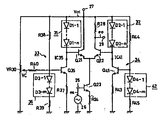
제1도는 본 발명이 적용된 음량제어회로의 구성도.1 is a block diagram of a volume control circuit to which the present invention is applied.
제2a도는 제1도에 도시된 음량제어회로와 감쇠도 대 제어전압간 특성도(A곡선과 B곡선) 및 종래기술의 특성도(C곡선), 제2b도는 제2a도에 대응되는 특성도로서, 수직축을 로그스케일로 바꾼 특성도.FIG. 2A is a characteristic diagram (a curve and a curve B) between the sound volume control circuit and the attenuation degree versus control voltage shown in FIG. Also, the characteristics of changing the vertical axis to log scale.
제3도는 제1도에 대한 상세회로도.3 is a detailed circuit diagram of FIG.
제4도는 제3도의 변형회로도.4 is a modified circuit diagram of FIG.
제5도는 제3도의 다른 변형회로도.5 is another modified circuit diagram of FIG.
제6도는 제3도의 또 다른 변형회로도.6 is another modified circuit diagram of FIG.
제7도는 본 발명이 적용된 전압제어형 발진기의 회로도.7 is a circuit diagram of a voltage controlled oscillator to which the present invention is applied.
제8도는 제7도의 회로특성을 설명하기 위한 도면이다.FIG. 8 is a diagram for explaining the circuit characteristics of FIG.
* 도면의 주요부분에 대한 부호의 설명* Explanation of symbols for main parts of the drawings
25 : 입력단자 26 : 신호원25: input terminal 26: signal source
27 : 전원 29 : 출력단자27: power supply 29: output terminal
31,32 : 다이오드회로 33,34 : 전류원31,32:
es : 입력신호 eo : 출력신호es: input signal eo: output signal
본 발명은 제어전압에 따라 예컨대 증폭기의 이득이나 감쇠기의 감쇠도, 또는 발진기의 주파수와 같은 전기적 특성이 변하게 되는 전압제어회로에 관한 것으로, 특히 음량이나 아날로그량을 조정하는데 사용되는 전압제어증폭기(또는 전압제어감쇠기)에 관한 것이다.BACKGROUND OF THE
일반적으로 이득이나 주파수와 같은 여러가지 전기적 특성은 제어전압으로 변화시켜야 할 필요가 있는 바, 오디오/비디오장치에 채택되는 음량제어회로에서는 음성증폭기의 이득이 볼륨제어신호의 제어전압에 따라 변하게 되는데, 이와 같은 음량제어회로는 DC제어전압에 의해 조절되는 차동증폭집적회로에 의해서 구성된다.In general, various electrical characteristics such as gain and frequency need to be changed to a control voltage. In a volume control circuit adopted for an audio / video device, the gain of the voice amplifier changes according to the control voltage of the volume control signal. The same volume control circuit is constituted by a differential amplification integrated circuit controlled by a DC control voltage.
이에 관해서는 1977년 12월 27일에 발간된 릴리스등에 의한 미국특허 제4,065,725호(이득제어회로)에 구체적으로 개시되어져 있다.This is specifically disclosed in U.S. Patent No. 4,065,725 (gain control circuit) published on December 27, 1977.
그런데, 상기한 종래회로의 감쇠도 대 제어전압의 정형적인 특성은 제2a도와 제2b도의 C곡선처럼 되어 있는데, (미국특허 제4,065,725호에서는 제2도), 이 특성도에 따르면 제어전압(Vc)이 1V이하일 때(또는 미국 특허 제4,065,725호에서는 VEGC가 3볼트이상일 때), C곡선의 직선성이 열화된다. 다시 말해서 감쇠도가 높은 범위(제2b도에서 -3OdB이하)에서 제어전압(Vc)의 변화에 대한 음량변화율은 매우 적어지게 되어, 결국 사용자가 오디오/비디오기기를 작은 음량으로 즐기고자 한다면, 음량제어기의 설정위치를 크게 변화시키지 않은 한 음량이 충분하게 변하지 않게되어, 조작상 불편하게 되고, 한편 사용자가 음량제어기를 세밀하게 다루어 음량을 충분히 낮추기를 원한다 할지라도, C곡선의 최대감쇠도는 약 -35dB이므로 음량제어회로가 C곡선으로 되어 있다면 사용자의 그러한 의도는 실질적으로 달성하기가 어렵게 된다. 이러한 점들이 종래기술의 단점으로 대두되고 있어 가능하면 감쇠도 대 제어전압간이 선형영역을 넓히고 최대감쇠도 역시 커지도록 할 필요가 있다.By the way, the conventional characteristic of the attenuation versus control voltage of the conventional circuit is like the C curve of Figs. 2a and 2b (Fig. 2 in US Pat. No. 4,065,725), and according to this characteristic diagram, the control voltage (Vc ) Is less than or equal to 1 V (or VEGC is greater than 3 volts in US Pat. No. 4,065,725), the linearity of the C curve deteriorates. In other words, in the high attenuation range (below -3OdB in FIG. 2b), the volume change rate for the change of the control voltage Vc becomes very small, so that if the user wants to enjoy the audio / video device at a small volume, The volume does not change sufficiently unless the setting position of the controller is greatly changed, which makes the operation inconvenient, while the maximum attenuation of the C curve is approximately low, even if the user wants to handle the volume controller in detail and lower the volume sufficiently. Since the -35dB volume control circuit has a C curve, the user's intentions are practically difficult to achieve. These points are a disadvantage of the prior art, and if possible, it is necessary to widen the linear region between the attenuation versus the control voltage and also increase the maximum attenuation.
본 발명은 상기한 종래회로의 문제점을 해결하기 위해 발명된 것으로서, 제어전압의 전기적 특성에 대한 제어가능범위의 직선성을 개선시킨 전압제어회로를 제공함에 그 목적이 있는 것이다.The present invention has been invented to solve the above problems of the conventional circuit, and an object thereof is to provide a voltage control circuit which improves the linearity of the controllable range with respect to the electrical characteristics of the control voltage.
상기한 목적을 달성하기 위해서 본 발명은 다음과 같은 회로요소를 포함하고 있다. 즉, 가변적인 제어전압을 제공하기 위한 제어전압과, 상기 제어전압의 변동에 따라 그 크기가 변하는 제1전류를 제공하기 위해서 상기 제어전압원에 접속되는 제1전류원, 상기 제1전류의 크기에 따라 변하는 제1전압을 제공하기 위해서 상기 제1전류원에 접속되는 제1전압원, 제2전류를 제공하기 위한 제2전류원, 상기 제2전류의 크기에 따라 변하는 제2전압을 제공하기 위해서 상기 제2전류원에 접속되는 제2전압원, 상기 제1전압원에 그 베이스측이 연결되는 제1트랜지스터와 제2전압원에 그 베이스측이 연결되는 제2트렌지스터로 이루어지는 증폭 회로등을 포함하여 본 발명이 구성된다.In order to achieve the above object, the present invention includes the following circuit elements. That is, according to a control voltage for providing a variable control voltage, a first current source connected to the control voltage source to provide a first current whose magnitude varies according to a change in the control voltage, and according to the magnitude of the first current. A first voltage source connected to the first current source to provide a varying first voltage, a second current source to provide a second current, and the second current source to provide a second voltage that varies according to the magnitude of the second current The present invention comprises an amplifying circuit comprising a second voltage source connected to the first voltage source, a first transistor connected to the base side of the first voltage source, and a second transistor connected to the base side of the second voltage source.
상기와 같은 구성에서, 음성신호와 같은 입력신호는 제1,제2트랜지스터의 에미터측 회로에 공급되고, 출력신호는 제2트랜지스터의 콜렉터측 회로로부터 도출되는 바, 증폭회로의 출력/입력특성은 제어전압에 의해서 변화한다.In the above configuration, an input signal such as an audio signal is supplied to the emitter side circuits of the first and second transistors, and the output signal is derived from the collector side circuit of the second transistor. It is changed by the control voltage.
또한, 상기 구성에서는 제1전류원이 증폭회로와 제어전압간 출력/입력특성의 선형범위를 확장시키기 위한 확장수단과 함께 제공된다(제2b도의 A곡선이나 B곡선 참조).Further, in the above configuration, the first current source is provided with expansion means for extending the linear range of the output / input characteristics between the amplifier circuit and the control voltage (see curve A or curve B in FIG. 2B).
이하, 예시도면을 참고해서 본 발명의 구성 및 작용·효과를 각 실시예에 따라 상세히 설명하는데, 각 실시예의 도면중 동일부분에는 같은 부호를 기입하여 설명한다.Hereinafter, the configuration, operation, and effect of the present invention will be described in detail with reference to the accompanying drawings, but the same reference numerals are used to describe the same parts in the drawings of each embodiment.
I) 기본적인 회로구성 및 작용·효과I) Basic circuit configuration, operation and effect
제1도는 본 발명이 적용된 음량제어회로의 구성도로서, 가변저항기(VR30)는 정(+)의 전원(27)과 접지점간에 설치되고, 이 가변저항기(VR30)의 가변단자는 OV~전원전압(Vcc)까지 변동되는 제어전압(Vc)을 제공한다. 전류원(33)은 상기 제어전압(Vc)에 응답하여 그 크기가 변하는 전류(133)를 공급하게 되는데, 이 전류원(33)은 다이오드회로(31)를 통하여 전원(27)에 결합되어 있다.1 is a configuration diagram of a volume control circuit to which the present invention is applied, and the variable resistor VR30 is installed between a
상기 다이오드회로(31)는 전류(133)에 의해 순방향으로 바이어스되는 n개의 직렬다이오드(D1-1~D1-n)로 구성된다. 한편 전류(134)를 공급하기 위한 전류원(34)은 다이오드회로(32)를 통해 전원(27)측에 접속되어 있는데, 이 다이오드회로(32)도 전류(134)에 의해 순방향으로 바이어스되는 n개의 직렬다이오드(D2-1~D2-n)로 구성된다.The
상기한 다이오드회로(31)와 전류원(33)간의 노오드는 NPN트랜지스터(Q21)의 베이스에 접속되어 있고, 다이오드회로(32)와 전류원(34)간의 노오드는 NPN트랜지스터(Q22)의 베이스에 접속되어 있다. 또한 트랜지스터(Q21)의 콜렉터는 전원(27)에 연결되며, 트랜지스터(Q22)의 콜렉터는 저항(R28)을 통해 전원(27)에 연결되어 있다. 상기 각 트랜지스터(Q21)(Q22)의 에미터는 서로 접속되어 NPN트랜지스터(Q23)의 콜렉터에 접속되어 있고, 이 트랜지스터(Q23)의 에미터는 저항(R24)을 통해 접지되어 있다.The node between the
위에서 설명한 트랜지스터(Q21-Q23)와 저항(R24)(R28)은 차동증폭회로를 구성하는 바, 트랜지스터(Q23)의 베이스는 입력단자(25)에 연결되고, 이 입력단자(25)에는 신호원(26)으로부터의 입력신호(es)가 인가된다.The transistors Q21-Q23 and resistors R24 and R28 described above constitute a differential amplifier circuit. The base of the transistor Q23 is connected to the
또한 차동증폭회로의 출력신호(eo)는 트랜지스터(Q22)의 콜텍터로부터 출력단자(29)로 출력된다.In addition, the output signal eo of the differential amplification circuit is output from the collaborator of the transistor Q22 to the
상기한 구조의 회로에서는 다음과 같은 식이 성립된다.In the circuit of the above structure, the following equation is established.

한편, 제1도회로의 구성요소에 나타나는 신호를 다음과 같이 정의해 보자.On the other hand, let us define the signal appearing in the components of the first circuit as follows.
VF1 ; 다이오드회로(31)의 각 다이오드에 나타나는 순방향전압강하,VF1; Forward voltage drop in each diode of the
VF2 ; 다이오드회로(32)의 각 다이오드에 나타나는 순방향전압강하,VF2; Forward voltage drop in each diode of the
VF21 : 트랜지스터(Q21)의 베이스-에미터간에 나타나는 순방향전압강하,VF21: Forward voltage drop appearing between base-emitter of transistor Q21,
VF22 : 트랜지스터(Q22)의 베이스-에미터간에 나타나는 순방향전압강하,VF22: Forward voltage drop appearing between base-emitter of transistor Q22,
Ic21 : 트랜지스터(Q21)의 콜렉터전류,Ic21: collector current of transistor Q21,
Ic22 ; 트랜지스터(Q22)의 콜렉터전류,Ic22; Collector current of transistor Q22,
Ic23 : 트랜지스터(Q23)의 콜렉터전류.Ic23: Collector current of transistor Q23.
상기 각 신호에 대한 정의하에 트랜지스터(Q21)(Q22)의 에미터포텐셜을 고려해 보면 다음의 식이 성립된다.Considering the emitter potentials of the transistors Q21 and Q22 under the definition of each signal, the following equation is established.
![]()
![]()
일반적으로, 베이스-에미터간 순방향전압강하(VF)는 잘 알려진 바와 같이,In general, the base-emitter forward voltage drop (VF) is well known,
![]()
![]()
으로 주어진다(단, K는 볼쯔만 상수, T는 절대온도, Ic는 바이폴라트랜지스터의 콜렉터 전류, Is는 콜렉터 포화전류이다).Where K is the Boltzmann constant, T is the absolute temperature, Ic is the collector current of the bipolar transistor, and Is is the collector saturation current.
제1도의 회로가 단일 칩의 반도체웨이퍼내에 집적회로화되고, 회로(31)(32)의 각 다이오드가 베이스-콜렉터접합트랜지스터의 구조로 구현될 때, VF=VF1=VF2가 된다.When the circuit of FIG. 1 is integrated into a semiconductor wafer of a single chip, and each diode of the
이 경우(3)식으로부터 트랜지스터(021)의 베이스전압(VB21=Vcc-n·VF1)과 트랜지스터(Q22)의 베이스전압(VB22=Vcc-n·VF2)은 다음식과 같이 표현된다.In this case (3), the base voltage VB21 = Vcc-n VF1 of the


(단, Ic31)은 다이오드회로(31)의 각 다이오드의 콜렉터전류, Is31은 포화전류, Ic32는 다이오드회로(32)의 각 다이오드의 콜렉터전류, Is32는 포화전류이다).(Where, Ic31 is the collector current of each diode of the
제1도의 차동증폭회로(Q21-Q23)의 효과적인 입력은 상기 베이스전압(VB21)(VB22)간의 전압차 △V이다.An effective input of the differential amplifier circuits Q21-Q23 of FIG. 1 is the voltage difference ΔV between the base voltages VB21 and VB22.
따라서,therefore,

의 관계가 성립된다.Relationship is established.
다이오드회로(31)의 각 다이오드특성과 다이오드회로(32)의 각 다이오드특성이 실질적으로 동일할 때, Is31=1s33이 되므로, In(Is31/Is32)n=0이 된다.When each diode characteristic of the
따라서 (6)식은So (6)
![]()
![]()
이 된다.Becomes
제1도의 회로에서 Ic31=Ic33, Ic32=I34이므로, (7)식은 다음의(8)식으로 변형된다.Since Ic31 = Ic33 and Ic32 = I34 in the circuit of FIG. 1, equation (7) is modified to the following equation (8).
![]()
![]()
상기한 내용과 유사하게, 트랜지스터(Q21)의 베이스- 에미터간 전압강하(VF21)와 트랜지스터(Q72)의 베이스-에이터간 전압강하(VF22)는,Similar to the above, the base-emitter voltage drop VF21 of transistor Q21 and the base-emitter voltage drop VF22 of transistor Q72 are:
![]()
![]()
![]()
![]()
이고, 양 전압강하의 전압차 △V는,And the voltage difference ΔV between the two voltage drops is

로 된다.It becomes
상기 트랜지스터(Q21)의 특성이 트랜지스터(Q22)의 특성과 실질적으로 같은 경우, Is21=Is22이므로, In(1s22/1s21)=0이 된다. 따라서(11)식은When the characteristic of the transistor Q21 is substantially the same as that of the transistor Q22, since Is21 = Is22, In (1s22 / 1s21) = 0. So (11)
![]()
![]()
이 되고, (8)식과 (12)식으로 다음 식이 성립된다.Then, the following equations are established by equations (8) and (12).
![]()
![]()
![]()
![]()
(13)과 (14)식에서 1c21+Ic22=Ic23[=트랜지스터(Q23)의 콜렉터전류]이므로(14)식에 의거In the formulas (13) and (14), 1c21 + Ic22 = Ic23 [= collector current of the transistor (Q23)].

이 된다.Becomes
한편, 제1도의 회로에서 신호감쇠도인 eo/es는 트랜지스터(Q21)(Q22)간의 분류비 Ic22/Ic21에 비례하므로 다음식이 성립된다.On the other hand, in the circuit of FIG. 1, eo / es, which is a signal attenuation diagram, is proportional to the classification ratio Ic22 / Ic21 between the transistors Q21 and Q22, and the following equation is established.
![]()
![]()
[단, 부(-)의 부호는 제1도의 차동증폭회로가 반전증폭기임을 나타낸다][Negative sign indicates that the differential amplifier circuit of FIG. 1 is an inverting amplifier]
제1도의 회로에서 출력(eo)의 최대치(eo max)는 트랜지스터(Q21)가 컷오프되어 Ic22=Ic23일때 나타나므로,In the circuit of FIG. 1, the maximum eo max of the output eo appears when the transistor Q21 is cut off and Ic22 = Ic23,
![]()
![]()
가 된다.Becomes
상기(17)식과(17)식으로부터From (17) and (17)
![]()
![]()
(단, AT는 차동증폭회로의 감쇠도로 정의한다.)AT is defined as the attenuation of the differential amplifier circuit.
상기(1),(15),(18)식으로부터 다음 식이 얻어진다.The following formula is obtained from the above formulas (1), (15) and (18).
![]()
![]()
위의(19)식이 제1도회로의 감쇠도 AT 대 제어전압 Vc간 특성을 나타내게 되는 바, K1=0.6, K2=0.1, n=5로 할 때, 제2a도나 제2b도의 A곡선이 얻어진다. K1=0.4, K2=0.2, n=5로 할 때에는 제2a도나 제2b도의 B곡선이 얻어진다.Equation (19) above shows the attenuation degree of the circuit of Fig. 1 between AT and the control voltage Vc. When K1 = 0.6, K2 = 0.1, and n = 5, the curve A of Fig. 2a or 2b is obtained. Lose. When K1 = 0.4, K2 = 0.2 and n = 5, the B curve of FIG. 2a or 2b is obtained.
제2b도의 A곡선과 8곡선은 높은 감쇠 영역(제2b도의 -30dB이하)에서 제어전압(Vc)에 대한 감쇠도(AT)의 변화율이 충분히 크다는 것을 시사한다. 나아가 AT 대 Vc의 선형영역이 넓고 최대 감쇠도가 충분히 크다는 것도 시사하는 것이다. 결국 본 발명에 의하면 오디오/비디오기기의 사용자가 편리하게 원하는 수준으로 음량을 조정할 수 있으며, 또한 음량을 편리하게 충분히 뮤우트시킬 수 있게 되는 효과를 거둘 수 있는 것이다.The curves A and 8 of FIG. 2B suggest that the rate of change of the attenuation degree AT with respect to the control voltage Vc is sufficiently large in the high attenuation region (below -30dB of FIG. 2B). Furthermore, this suggests that the linear region of AT vs. Vc is wide and the maximum attenuation is large enough. As a result, according to the present invention, the user of the audio / video device can conveniently adjust the volume to a desired level, and can also achieve the effect of being able to mute the volume sufficiently conveniently.
Vc를 반분시켜서 감쇠도 AT=1/10을 얻어야 하는 경우를 가정해 보면, (19)식은 다음과 같이 변형된다.Assuming that the attenuation degree AT = 1/10 should be obtained by dividing Vc, equation (19) is modified as follows.
![]()
![]()
상기(20)식이 성립되도록 각각의 계수 Kl,Vc,K2 및 n이 결정되면 AT=1/10이 얻어진다. 만일 K2=0일 때 AT=1/10은When the coefficients K1, Vc, K2 and n are determined such that Eq. (20) is established, AT = 1/10 is obtained. If K2 = 0 then AT = 1/10
![]()
![]()
로 얻어진다.Is obtained.
상기 식에 대해 특정의 Vc값이 주어지면 등식이 성립되는 K1과 n이 결정된다. 물론 AT=1/10을 만족시키는 여러 가지 조건이 달리 성립될 수 있다.Given a specific Vc value for the above equation, K1 and n are determined to hold the equation. Of course, various conditions for satisfying AT = 1/10 may be otherwise established.
II) 구체적인 회로구현수단 및 작용·효과II) Specific Circuit Implementation Means, Actions and Effects
제3도는 위에서 설명한 제1도의 상세한 회로도로서, 전류원(33)은 NPN트랜지스터(Q35)와 다이오드회로(36) 및 저항(R37~R40)으로 구성된다. 여기에서 트랜지스터(Q35)의 에미터는 저항(R37)을 통해 접지되고, 그 콜렉터는 다이오드회로(31)를 통하여 전원(27)에 접속된다. 다이오드회로(31)의 직렬접속 트랜지스터(D1-1~D1-n)는 트랜지스터(Q35)의 콜렉터전류(Ic35)에 의해 순방향으로 바이어스되는데, 이 콜렉터전류(Ic35)는 제1도의 전류(I33)에 대응되는 것이다. 한편, 트랜지스터(Q35) 베이스는 저항(R40)을 통해 가변저항기(VR30)의 가변단자에 접속되며, 다이오드회로(36)와 저항(R39)을 통해 접지 측에도 접속된다.FIG. 3 is a detailed circuit diagram of FIG. 1 described above, wherein the
상기한 다이오드회로(36)는 저항(R38)으로부터 저항(R39)쪽으로 흐르는 전류에 의해 순방향으로 바이어스되는 m개의 직렬다이오드(D3-1~D3-m)로 구성된다.The
전류원(34)은 NPN트랜지스터(Q41)와 다이오드회로(42) 및 저항(R43~R45)으로 구성되는데, 트랜지스터(Q41)의 에미터는 저항(R43)을 통해 접지되고, 그 콜렉터는 다이오드회로(32)을 통하여 전원(27)에 접속된다. 또한 다이오드회로(32)를 구성하는 n개의 직렬다이오드(D2-1~D2-n)는 트랜지스터(Q41)의 콜렉터전류(Ic41)에 의해 순방향으로 바이어스되는데, 이 전류(Ic41)는 제1도의 전류(I34)에 대응되는 것이다. 한편, 트랜지스터(Q41)의 베이스는 저항(R44)을 통해 전원(27)에 접속되는 한편, 다이오드회로(42)와 저항(R45)을 통해 접지측에 접속된다.The
상기 다이오드회로(42)는 m개의 직렬다이오드(D4-1~D4-m)로 구성된다.The
상기한 회로구성에서 다이오드회로(36)의 다이오드갯수틀 ㎖로 하고 다이오드회로(47)의 다이오드갯수로 m2로 하뮤, 각 다이오드들은 베이스-콜댁터접속 트랜지스터로 만들어 진다고 하자. 그리고 가변저항기(VR30)의 전압분할계수를 P라 하면(P는 0-1사이에서 변함), 제어전압(Vc)은 전원전압(Vcc)과 계수 P에 의존하여 가변된다. 즉,In the above circuit configuration, it is assumed that the number of diodes in the
![]()
![]()
의 관계가 성립된다.Relationship is established.
상기한 가정과 관계식하에서 트랜지스터(Q35)의 콜랙터전류(Ic35=제1도의 I33)는 다음과 같이 된다.Under the above assumptions and relations, the collector current (Ic35 = I33 in FIG. 1) of the transistor Q35 is as follows.

그리고,And,
![]()
![]()
나아가Furthermore
![]()
![]()
![]()
![]()
이라고 가정하고, 이를(23)(24)식에 대입하면 VF항을 소거시킬 수 있으므로 다음 식이 얻어진다.It is assumed that the VF term can be eliminated by substituting this into the equations (23) and (24), and the following equation is obtained.
![]()
![]()
![]()
![]()
(22)식으로부터 P=Vc/Vcc이므로,Since P = Vc / Vcc from (22),
![]()
![]()
(27)과 (28)식으로부터는From equations (27) and (28)
![]()
![]()
이 성립되고, (25)(26)식에 의해(30)식은,Is established, and by (25) and (26),
![]()
![]()
여기에서 Ic35=I33,Ic41=134, P=Vc/Vcc이므로 (1)식과 (31)식에 의해 다음식이 도출된다.Since Ic35 = I33, Ic41 = 134 and P = Vc / Vcc, the following equations are derived from equations (1) and (31).
![]()
![]()
![]()
![]()
상기 식에서 m1=m2=2, R37=R43이라 가정하면,In the above formula, assuming m1 = m2 = 2 and R37 = R43,
![]()
![]()
![]()
![]()
로 된다.It becomes
(33A)와(33B)의 식은(1)식의 파라메터 Kl과 K2가 저항(R39)(R40)과 전원전압(Vcc)에 따라 결정된다는 것을 시사한다.The equations (33A) and (33B) suggest that the parameters Kl and K2 in the equation (1) are determined in accordance with the resistors R39 (R40) and the power supply voltage Vcc.
현재의 집적회로제조기술에 따르면, 정밀한 저항비 R39/R40을 실현하기는 쉽다.According to the current integrated circuit manufacturing technology, it is easy to realize the precise resistance ratio R39 / R40.
따라서, 전원전압(Vcc)이 충분히 안정된다면, 안정한 파라메터 Kl과 K2를 얻을 수 있으며, 이로써 제2a도 및 제2b도의 우수한 특성곡선(A나 B)을 얻을 수 있게 되는 것이다.Therefore, if the power supply voltage Vcc is sufficiently stable, stable parameters Kl and K2 can be obtained, thereby obtaining excellent characteristic curves A or B of FIGS. 2a and 2b.
상술한 제3도의 회로에서, 회로요소(36)와 저항(R37-R47)은 제어전압(Vc)에 관련되는 출력신호(eo)의 선형변화범위를 확장시키기 위한 선형보상수단으로 동작한다.In the circuit of FIG. 3 described above, the
III) 제1변형예의 구성 및 작용·효과III) Composition, Action and Effect of First Modification
제4도는 제3도의 변형예로서, 전류원(33)은 NPN트랜지스터(Q51)(Q52)와 다이오드회로(53) 및 저항(R54~R56)으로 구성되는데, 상기 트랜지스터(Q51)의 에미터는 저항(56)을 통해 접지되고, 트랜지스터(Q52)의 에미터도 저항(R55)을 통해 접지된다. 그리고 각 트랜지스터(Q51)(Q52)의 콜렉터는 서로 접속되어서 다이오드회로(31)를 매개하여 전원(27)측에 접속된다.4 is a variation of FIG. 3, wherein the
다이오드회로(31)의 직렬접속 다이오드 n개(D1-1~D1-n)는 트랜지스터(Q51)(Q52)의 콜렉터전듀합인 전류(I33)에 의해 순방향으로 바이어스된다.The n series-connected diodes D1-1 to D1-n of the
상기한 트랜지스터(Q51)의 베이스에는 제어전압(Vc)이 입력되고, 트랜지스터(Q52)의 베이스는 저항(R54)을 통해 전원(27)에 접속되는 한편, 다이오드회로(53)를 통해 접지측에도 접속된다. 이 다이오드회로(53)는 m개의 직렬다이오드(D5-1~D5-m)로 구성된다.The control voltage Vc is input to the base of the transistor Q51, and the base of the transistor Q52 is connected to the
전류원(34)은 NPN트랜지스터(Q57)와 다이오드회로(58) 및 저항(R59-R61)으로 구성되는데, 트랜지스터(Q57)의 에미터는 저항(R60)을 통해 접지되고, 그 콜렉터는 다이오드회로(32)를 통해 전원(27)에 접속된다.The
상기 다이오드회로(32)를 구성하는 n개의 다이오드(D6-1~D6-m)는 트랜지스터(Q57)에 흐르는 콜렉터전류(I34)에 의해 순방향으로 바이어스된다. 이 트랜지스터(Q57)의 콜렉터는 저항(R61)을 통해 접지되고, 그 베이스는 저항(R59)을 통해 전원(27)에 연결되는 한편, 다이오드회로(58)를 통해 접지된다.The n diodes D6-1 to D6-m constituting the
상기 다이오르회로(58)는 m개의 직렬접속다이오드(D6-1~D6-m)로 구성된다.The diode circuit 58 is composed of m series connection diodes D6-1 to D6-m.
상기한 회로구성에서 다이오드회로(53)의 다이오드갯수틀 m3으로 하고, 다이오드회로(58)의 다이오드갯수를 m4로 하며, 각 다이오드가 베이스-콜렉터접합 트랜지스터로 구성된다고 하면,In the above circuit configuration, if the number of diodes in the
![]()
![]()
![]()
![]()
로 된다. 상기 식에서 n은 다이오드회로(32)의 다이오드갯수를 나타낸다.It becomes In the above formula, n represents the number of diodes in the
상기(34)(35)식에서 다음의 관계가 성립된다고 가정하자.Suppose that the following relationship is established in the above expressions (34) and (35).
![]()
![]()
![]()
![]()
그러면 (34)식과 (35)식은Then equations (34) and (35)
![]()
![]()
![]()
![]()
가 된다.Becomes
상기(22),(37A),(378)식으로부터 다음의 관계식이 얻어진다.The following relational expressions are obtained from the above formulas (22), (37A) and (378).
![]()
![]()
(1)식과 (38)식으로부터From (1) and (38)
![]()
![]()
![]()
![]()
상기(38)식은 전류비(I33/I34)가 저항비(R61/R56)와 전압분배계수(P)에 의존한다는 것을 시사한다.The above equation (38) suggests that the current ratio I33 / I34 depends on the resistance ratio R61 / R56 and the voltage distribution coefficient P.
IV) 제2변형예IV) Second Modification
제5도는 제3도회로의 제2변형회로도로서, NPN트랜지스터(Q35)의 베이스는 트랜지스터(Q36)의 콜렉터에 접속되고, 그 에미터는 저항(R37)을 통해 접지된다.5 is a second modified circuit diagram of the FIG. 3 circuit, in which the base of the NPN transistor Q35 is connected to the collector of the transistor Q36, and the emitter is grounded through the resistor R37.
상기 트랜지스터(Q36)의 에미터는 전원(27)에 연결되고, 그 베이스는 다이오드(D2-1)의 캐소드에 접속된다. 또한 트랜지스터(Q36)의 콜렉터는 저항(R62)을 통해서 PNP트랜지스터(Q58)의 에미터에 접속되고, 트랜지스터(Q58)의 콜렉터는 접지된다. 한편, 트랜지스터(Q58)의 베이스는 가변저항기(VR30)로부터 제어전압(Vc)을 받아들이는데, 가변저항기(VR30)의 일단은 저항(R63)을 통해 전원(27)에 접속된다.The emitter of transistor Q36 is connected to a
상기한 구조외 제5도에서 트랜지스터(Q35)의 콜렉터전류(Ic35)는 다음카 같이 표시된다.In FIG. 5, the collector current Ic35 of the transistor Q35 is represented as follows.
![]()
![]()
[단, VFQ35는 트랜지스터(Q35)의 베이스-에미터간 전압, VFQ58은 트랜지스터(Q58)의 베이스-에미터간 전압, Ic36은 트랜지스터(Q36)의 콜럭터전류를 나타낸다]Where VF Q35 is the base-emitter voltage of transistor Q35, VF Q58 is the base-emitter voltage of transistor Q58, and Ic36 is the collector current of transistor Q36.
상기 트랜지스터(Q36)와 다이오드(D2-1)가 전류미러회로(current mirror circuit)를 구성할 때,When the transistor Q36 and the diode D2-1 form a current mirror circuit,
![]()
![]()
이 성립된다. 나아가 적절한 디자인이 트랜지스터(Q58)(Q35)의 반도체제조공정에 적용된다면,This holds true. Furthermore, if a suitable design is applied to the semiconductor manufacturing process of transistors Q58 and Q35,
![]()
![]()
이 성립될 수 있다. 상기(41)(42)식을 (40)식에 대입하면,This can be established. Substituting the above formulas (41) and (42) into the formula (40),
![]()
![]()
이 되고, (43)식은Becomes (43)
![]()
![]()
으로 변형될 수 있다.It can be transformed into.
(28)식을 (44)식에 대입하면, 다음 식이 얻어진다.Substituting Eq. (28) into Eq. (44) yields the following equation.
![]()
![]()
(1)식에서In the formula (1)
![]()
![]()
![]()
![]()
상기한 (45)식은 전류비(Ic35/Ic41)가 저항비가 Vcc에만 의존하고 Vc에는 비례한다는 것을 시사한다. 또한(46A)(46B)식은(19)식에 사용되는 파라메터 K1과 K2가 저항비와 Vcc에 의해 정해진다는 것을 나타낸다.The above equation (45) suggests that the current ratio (Ic35 / Ic41) depends only on the resistance ratio Vcc and is proportional to Vc. The equations (46A) and (46B) indicate that the parameters K1 and K2 used in equation (19) are determined by the resistance ratio and Vcc.
V) 제3변형예V) Third Modification
제6도는 제3도의 또 다른 변형예로서, 제6도에서 NPN트랜지스터(Q38)의 콜렉터는 다이오드회로(31)를 거쳐 전원(27)에 접속된다. 또한 트랜지스터(Q38)의 에미터는 저항(R65)을 거쳐 접지되는 한편 저항(R66)을 거쳐 가변저항기(VR30)의 가변단자에 접속된다. 트랜지스터(Q38)의 베이스는 NPN트랜지스터(Q37)의 베이스에 접속되는데, 이 트랜지스터(Q37)의 콜렉터는 다이오드회로(32)를 거쳐 전원(27)에 접속되고 양 트랜지스터(Q37)(Q38)의 공통베이스는 한편으로 다이오드회로(100)와 저항(R67)의 직렬회로를 통해 접지되는 동시에 저항(R68)과 다이오드회로(101)를 거쳐 전원(27)에도 접속된다.6 is another modification of FIG. 3, in which the collector of the NPN transistor Q38 is connected to the
상기한 다이오드회로(100)는 12개의 직렬접속다이오드(D7-1~D7-12)로 구성되고, 다이오드회로(101)는 11개의 직렬접속다이오드(D8-1~D8-11)로 구성된다.The diode circuit 100 includes twelve series connection diodes D7-1 to D7-12, and the diode circuit 101 includes eleven series connection diodes D8-1 to D8-11.
상기 구성의 제6도회로에서 Q37의 에미터전위를 VE37,Q38의 에미터전위를 VE38,Q37의 베이스-에미터간 전압을 VFQ37,Q38의 베이스-에미터간 전압을 VFQ38,VFQ37=VFQ38(=VF)라 한다면, VE37=VE38=VE가 얻어진다. 이 경우 에미터전위(VE)는,In the circuit of FIG. 6, the emitter potential of Q37 is defined as the emitter potential of VE37 and Q38, and the base-emitter voltage of VE38 and Q37 is VF Q37 and the base-emitter voltage of Q38 is VF Q38 and VF Q37 = VF If Q38 (= VF), then VE37 = VE38 = VE is obtained. In this case, the emitter potential (VE) is
![]()
![]()
(단, I1은 회로(101)의 다이오드갯수, I2는 회로(100)의 다이오드갯수, VF는 각 다이오드의 순방향전압강하로서 VFQ37및 VFQ38과 동일함.)(Where I1 is the number of diodes in circuit 101, I2 is the number of diodes in circuit 100, and VF is the forward voltage drop of each diode equal to VF Q37 and VF Q38 .)
상기 (47)식에서In the formula (47)
![]()
![]()
이 성립된다면, (47)식은If this holds, equation (47)
![]()
![]()
로 간략화된다.Is simplified.
상기(49)식이 성립될 때 트랜지스터(Q37)의 콜렉터전류(Ic37)와 트랜지스터(Q38)의 콜렉터전류(Ic38)는,When the expression (49) is established, the collector current Ic37 of the transistor Q37 and the collector current Ic38 of the transistor Q38 are
![]()
![]()
![]()
![]()
상기(50)(51)식에서In the formula (50) (51)
![]()
![]()
(49)식을 (52)식에 대입하면,Substituting (49) into (52),
![]()
![]()
(1)식에서,In formula (1),
![]()
![]()
![]()
![]()
상기한(53)식은 전류비 Ic38/Ic37이 저항비와 Vcc에만 의존하고 Vc에 비례한다는 것을 시사한다.The above equation (53) suggests that the current ratio Ic38 / Ic37 depends only on the resistance ratio and Vcc and is proportional to Vc.
또한(54A)식과 (54B)식을 파라메터 Kl과 K2가 저항비와 Vcc에 의해 정해진다는 것을 나타낸다.Equations (54A) and (54B) indicate that the parameters Kl and K2 are determined by the resistance ratio and Vcc.
VI) 본 발명히 적용된 VCOVI) VCO applied in the present invention
제7도는 본 발명이 적용된 전압제어형 발진기(VCO)의 회로도를 나타낸 것으로, 제3도의 차동증폭회로부(Q21-Q23,R24-R28)대신 특정회로부가 대치되어 있다. 이 회로구성에서 NPN트랜지스터(Q35)의 콜렉터는 단자(P3)를 통해 트랜지스터(Q71)(Q74)의 각 베이스에 접속되고, NPN트랜지스터(Q41)의 콜렉터는 단자(P4)를 통해 트랜지스터(Q72)(Q73)의 공통베이스에 접속된다.7 shows a circuit diagram of a voltage controlled oscillator (VCO) to which the present invention is applied, in which a specific circuit portion is replaced instead of the differential amplification circuit portions Q21-Q23 and R24-R28 of FIG. In this circuit configuration, the collector of the NPN transistor Q35 is connected to each base of the transistors Q71 and Q74 through the terminal P3, and the collector of the NPN transistor Q41 is connected to the transistor Q72 through the terminal P4. It is connected to the common base of (Q73).
트랜지스터(Q71)(Q73)의 콜렉터는 서로 접속되어 전원(27)에 연결되고, 트랜지스터(Q72)(Q74)의 콜렉터는 단자(P2)와 공진회로(Z) 및 단자(P1)를 통해 위상천이기(712,734 : phase shifter)에 접속된다. 따라서 발진출력(eosc)은 공진회로(Z)를 거쳐 단자(Pl)에 되돌러진다. 그리고 위상천이기(712)의 출력은 단자(P5)를 통해 트랜지스터(Q71)(Q72)의 에미터에 공급되고, 위상천이기(734)의 출력은 단자(P6)를 통해 트랜지스터(Q73)(Q74)의 에미터에 공급된다. 상기 트랜지스터(Q71-Q74)는 2중균형 차동증폭회로를 구성하고, 한편 공진회로(Z)는 저역통과필터(R1,C1)와 수정발진기(X1)의 직렬회로로 구성된다.The collectors of transistors Q71 and Q73 are connected to each other and connected to the
상기한 회로요소들(Q71-Q74,R70,712,734)은 위상제어회로(PC)를 구성하는데 이 위상제어회로(PC)에서 위상천이기(712)의 위상천이량은 다른 위상천이기(734)의 천이량과는 다르다. 따라서 단자(P1)와 단자(P2)간의 신호위상이탈은 단자(P3)와 단자(P4)간의 전위차에 의해 제어된다.The circuit elements Q71-Q74, R70, 712 and 734 constitute a phase control circuit PC, in which the phase shift amount of the
상기 단자(P3)와 단자(P4)간의 전위차는 제어전압(Vc)에 따라 바뀐다. 결국, 출력(eosc)의 발진주파수 fosc는 제어전압(Vc)에 의해 바뀔 수 있는 것이다.The potential difference between the terminal P3 and the terminal P4 changes in accordance with the control voltage Vc. As a result, the oscillation frequency fosc of the output eosc can be changed by the control voltage Vc.
제8도는 제7도에 도시된 전압형 제어발진기의 특성을 나타내는 도면으로서, A1곡선은 제어전압(Vc : 또는 트랜지스터 Q35의 콜렉터전류(Ic35) 대 발진주파수(fosc)간의 특성곡선이고, A2곡선은 트랜지스터(Q72)의 콜렉터전류(Ic72) 대 발진주파수(fosc)간의 특성곡선이며, A3곡선은 상기 콜렉터전류(Icf2) 대 제어전압(VC)간의 특성곡선이다.FIG. 8 is a diagram showing the characteristics of the voltage controlled oscillator shown in FIG. 7, wherein the curve A1 is the characteristic curve between the control voltage Vc or the collector current Ic35 of the transistor Q35 and the oscillation frequency fosc, and the curve A2. Is a characteristic curve between the collector current Ic72 and the oscillation frequency fosc of the transistor Q72, and A3 is a characteristic curve between the collector current Icf2 and the control voltage VC.
한편, 일반적인 전압형 제어발진기의 제어전압(Vc) 대 발진주파수(fosc)의 특성은 A2곡선과 유사하다.On the other hand, the characteristics of the control voltage (Vc) versus the oscillation frequency (fosc) of the general voltage controlled oscillator is similar to the A2 curve.
상기 특성도에서 제어전압(Vc)이 Xa축의 a1에 설정되었다고 가정해 보자. 이 경우 A3곡선에 따라 전류(Ic72)는 Yb축의 a2점에 있게 되고, 이 Yb축의 a2점은 Xb축의 a3점에 대응되게 된다. 또한 A2곡선에 따라 Xb축 a3점에서의 전류(Ic72)는 Ya축의 a4점에 대응된다. 그러면 a1점에서외 제어전압(Vc)은 A1곡선의 B1점에 대응되고 그래서 a4점에서의 발진주파수(fosc)와 연관된다. 비숫한 방법으로 b1-e2에서의 제어전압(Vc)은 A1곡선의 B2-B5점에 대응되고 b4-e4점에서의 주파수(fosc)에 각각 관련되므로 B1-B5점상에 전개되는 직선에 거의 가까운 A1특성곡선이 얻어진다.Assume that the control voltage Vc is set to a1 of the Xa axis in the characteristic diagram. In this case, according to the A3 curve, the current Ic72 is at the a2 point of the Yb axis, and the a2 point of the Yb axis corresponds to the a3 point of the Xb axis. In addition, according to the curve A2, the current Ic72 at the point a3 of the Xb axis corresponds to the point a4 of the Ya axis. Then the control voltage Vc at the point a1 corresponds to the point B1 of the curve A1 and thus is associated with the oscillation frequency fosc at the point a4. In a similar way, the control voltage Vc at b1-e2 corresponds to the point B2-B5 of the A1 curve and to the frequency fosc at the point b4-e4, so it is almost close to the straight line developing on the points B1-B5. An A1 characteristic curve is obtained.
제8도의 설명에서 알 수 있는 것처럼, 제7도회로의 동작에 따라 A2곡선의 비직선성이 A3곡선의 비직선성에 의해 보상되므로 제어전압(Vc) 대 주파수(fosc)간의 선형특성 A1이 얻어진다.As can be seen from the description of FIG. 8, according to the operation of the circuit of FIG. 7, the nonlinearity of the A2 curve is compensated by the nonlinearity of the A3 curve, so that the linear characteristic A1 between the control voltage Vc and the fosc is obtained. Lose.
상기한 실시예에서는 제어전압(Vc)에 의한 전류원(33)의 제어대신 전류원(34)을 제어할 수도 있고, 양 전류원(33)(34)을 한꺼번에 제어할 수도 있다.In the above-described embodiment, the
이러한 경우, 제3도의 트랜지스터(035)의 베이스전위는 인버터회로에 의해 그 위상이 반전되고, 이 인버터회로의 위상반전출력은 일례로 트랜지스터(Q41)의 베이스에 인가된다.In this case, the base potential of the transistor 035 of FIG. 3 is inverted in phase by the inverter circuit, and the phase inversion output of the inverter circuit is applied to the base of the transistor Q41, for example.
본 발명은 이상에서 설명한 실시예에만 한정되지 않고, 특허청구의 범위에 기재된 내용을 근거로 그 요지를 벗어나지 않는 범위에서 여러가지 형태로 실시될 수 있다.The present invention is not limited only to the embodiments described above, and can be implemented in various forms without departing from the gist of the present invention based on the contents described in the claims.
Claims (21)
Applications Claiming Priority (2)
| Application Number | Priority Date | Filing Date | Title |
|---|---|---|---|
| JP60-50330 | 1985-03-15 | ||
| JP60050330A JPH0626291B2 (en) | 1985-03-15 | 1985-03-15 | Gain control device |
Publications (2)
| Publication Number | Publication Date |
|---|---|
| KR860007779A KR860007779A (en) | 1986-10-17 |
| KR910000687B1 true KR910000687B1 (en) | 1991-01-31 |
Family
ID=12855897
Family Applications (1)
| Application Number | Title | Priority Date | Filing Date |
|---|---|---|---|
| KR1019860001422A KR910000687B1 (en) | 1985-03-15 | 1986-02-28 | Voltage-control circuit |
Country Status (5)
| Country | Link |
|---|---|
| US (1) | US4727334A (en) |
| JP (1) | JPH0626291B2 (en) |
| KR (1) | KR910000687B1 (en) |
| DE (1) | DE3608649A1 (en) |
| GB (1) | GB2172457B (en) |
Families Citing this family (3)
| Publication number | Priority date | Publication date | Assignee | Title |
|---|---|---|---|---|
| JP3078858B2 (en) * | 1991-03-07 | 2000-08-21 | パイオニア株式会社 | VCA circuit |
| US6563382B1 (en) | 2000-10-10 | 2003-05-13 | International Business Machines Corporation | Linear variable gain amplifiers |
| GB2369259B (en) | 2000-11-21 | 2005-07-13 | C Mac Quartz Crystals Ltd | A method and apparatus for generating an input signal for a tunable circuit |
Family Cites Families (6)
| Publication number | Priority date | Publication date | Assignee | Title |
|---|---|---|---|---|
| US3691475A (en) * | 1970-07-24 | 1972-09-12 | Hitachi Ltd | Voltage controlled oscillator |
| US4017804A (en) * | 1975-12-05 | 1977-04-12 | Hewlett-Packard Company | Broad band variable gain amplifier |
| US4065725A (en) * | 1976-08-16 | 1977-12-27 | Motorola, Inc. | Gain control circuit |
| DE2731543C3 (en) * | 1977-07-13 | 1980-07-31 | Haarmann & Reimer Gmbh, 3450 Holzminden | Process for the preparation of cyclopentadecanolide |
| US4318051A (en) * | 1980-01-15 | 1982-03-02 | Rca Corporation | Symmetrically gain controlled differential amplifier |
| US4426625A (en) * | 1981-08-27 | 1984-01-17 | Rca Corporation | Circuit for linearly gain controlling a differential amplifier |
-
1985
- 1985-03-15 JP JP60050330A patent/JPH0626291B2/en not_active Expired - Lifetime
-
1986
- 1986-02-28 KR KR1019860001422A patent/KR910000687B1/en not_active IP Right Cessation
- 1986-03-12 US US06/839,080 patent/US4727334A/en not_active Expired - Fee Related
- 1986-03-12 GB GB8606025A patent/GB2172457B/en not_active Expired
- 1986-03-14 DE DE19863608649 patent/DE3608649A1/en active Granted
Also Published As
| Publication number | Publication date |
|---|---|
| DE3608649C2 (en) | 1991-04-25 |
| KR860007779A (en) | 1986-10-17 |
| US4727334A (en) | 1988-02-23 |
| JPH0626291B2 (en) | 1994-04-06 |
| DE3608649A1 (en) | 1986-09-25 |
| GB8606025D0 (en) | 1986-04-16 |
| JPS61210713A (en) | 1986-09-18 |
| GB2172457B (en) | 1989-11-22 |
| GB2172457A (en) | 1986-09-17 |
Similar Documents
| Publication | Publication Date | Title |
|---|---|---|
| US3813607A (en) | Current amplifier | |
| US5373253A (en) | Monolithic current mirror circuit employing voltage feedback for β-independent dynamic range | |
| US4524318A (en) | Band gap voltage reference circuit | |
| US4639685A (en) | Offset reduction in unity gain buffer amplifiers | |
| EP0908003B1 (en) | Temperature compensated amplifier | |
| US4949054A (en) | Temperature stable oscillator | |
| US6104244A (en) | Amplifier having a rail-to-rail output stage | |
| US4553044A (en) | Integrated circuit output driver stage | |
| KR850001539B1 (en) | Current mode biquadratic active filter | |
| US4692711A (en) | Current mirror circuit | |
| US4872209A (en) | Integratable amplifier circuit having frequency responsive negative feedback | |
| KR910000687B1 (en) | Voltage-control circuit | |
| US4002993A (en) | Differential amplifier | |
| US4425551A (en) | Differential amplifier stage having bias compensating means | |
| EP0264171A2 (en) | Gain selectable amplifier with resonance compensation | |
| KR0169987B1 (en) | Amplifier arrangement | |
| US4766367A (en) | Current mirror with unity gain buffer | |
| US3936731A (en) | Amplifier with fast recovery after input signal overswing | |
| US5402084A (en) | Coupling circuit | |
| US5578966A (en) | Output stage for a high-speed video amplifier | |
| US4481480A (en) | Feedback amplifier having a voltage-controlled compensation circuit | |
| WO1993003543A1 (en) | Voltage-controlled variable capacitor | |
| US6104249A (en) | Highly linear transconductance circuit and filter using same | |
| WO1993019522A1 (en) | Coupling circuit | |
| EP0667057A1 (en) | Active impedance termination |
Legal Events
| Date | Code | Title | Description |
|---|---|---|---|
| A201 | Request for examination | ||
| E902 | Notification of reason for refusal | ||
| G160 | Decision to publish patent application | ||
| E701 | Decision to grant or registration of patent right | ||
| GRNT | Written decision to grant | ||
| FPAY | Annual fee payment |
Payment date: 19960124 Year of fee payment: 6 |
|
| LAPS | Lapse due to unpaid annual fee |