KR840000113B1 - Periodically biased video disc player servo system - Google Patents
Periodically biased video disc player servo system Download PDFInfo
- Publication number
- KR840000113B1 KR840000113B1 KR1019800003254A KR800003254A KR840000113B1 KR 840000113 B1 KR840000113 B1 KR 840000113B1 KR 1019800003254 A KR1019800003254 A KR 1019800003254A KR 800003254 A KR800003254 A KR 800003254A KR 840000113 B1 KR840000113 B1 KR 840000113B1
- Authority
- KR
- South Korea
- Prior art keywords
- signal
- voltage
- video
- phase detector
- circuit
- Prior art date
Links
Images

Classifications
-
- H—ELECTRICITY
- H04—ELECTRIC COMMUNICATION TECHNIQUE
- H04N—PICTORIAL COMMUNICATION, e.g. TELEVISION
- H04N9/00—Details of colour television systems
- H04N9/79—Processing of colour television signals in connection with recording
- H04N9/80—Transformation of the television signal for recording, e.g. modulation, frequency changing; Inverse transformation for playback
- H04N9/82—Transformation of the television signal for recording, e.g. modulation, frequency changing; Inverse transformation for playback the individual colour picture signal components being recorded simultaneously only
- H04N9/85—Transformation of the television signal for recording, e.g. modulation, frequency changing; Inverse transformation for playback the individual colour picture signal components being recorded simultaneously only the recorded brightness signal occupying a frequency band totally overlapping the frequency band of the recorded chrominance signal, e.g. frequency interleaving
-
- G—PHYSICS
- G11—INFORMATION STORAGE
- G11B—INFORMATION STORAGE BASED ON RELATIVE MOVEMENT BETWEEN RECORD CARRIER AND TRANSDUCER
- G11B9/00—Recording or reproducing using a method not covered by one of the main groups G11B3/00 - G11B7/00; Record carriers therefor
- G11B9/06—Recording or reproducing using a method not covered by one of the main groups G11B3/00 - G11B7/00; Record carriers therefor using record carriers having variable electrical capacitance; Record carriers therefor
Landscapes
- Engineering & Computer Science (AREA)
- Multimedia (AREA)
- Signal Processing (AREA)
- Television Signal Processing For Recording (AREA)
- Processing Of Color Television Signals (AREA)
- Rotational Drive Of Disk (AREA)
Abstract
Description
제1도는 본 발명을 실시한 비데오 디스크 플레이어의 부분적인 개략형태의 계통도.1 is a schematic diagram of a partial schematic view of a video disc player according to the present invention.
제2도는 제1도의 플레이어에 대한 신호파형과 타이밍의 상관도.2 is a correlation between signal waveforms and timings for the player of FIG.
본 발명은 비데오 디스크 플레이어에 관한 것으로, 특히 이러한 플레이어에 대한 비데오 신호교정 서보 장치에 관한 것이다.The present invention relates to a video disc player, and more particularly, to a video signal calibration servo device for such a player.
비데오 신호 교정 서보장치를 포함하는 비데오 디스크 플레이어는 1976년 6월 22일 티. 더블류. 부루스에게 허여된 미합중국 특허 제 3,965,482호 명칭 명칭"비데오 디스크용 속도 교정회로"에 설명된다. 부루스의 플레이어는 비데오 디스크를 회전시키기 위한 턴테이블과 "매장된 부반송파"(BSC) 포맷으로 디스크상에 기록된 정보를 나타내는 용량변화를 감지하기 위한 픽업변환기와 FM 출력신호를 발생시키기 위해 용량변화에 반응하는 발진기를 포함한다. FM 신호는 비데오 콘버터에 의해 BSC 포맷에서 NTSC 포맷으로 변환되는 합성 비데오 신호를 발생시키도록 복조된다.Video disc players, including video signal correction servos, are available on June 22, 1976. W. US Pat. No. 3,965,482, entitled "Speed Calibration Circuit for Video Discs," issued to Burus. The player of BRUSH responds to the capacity change to generate an FM output signal with a turntable to rotate the video disc, a pickup converter to detect the change in capacity that represents the information recorded on the disc in the "stored subcarrier" (BSC) format. It includes an oscillator. The FM signal is demodulated by the video converter to generate a composite video signal that is converted from the BSC format to the NTSC format.
부루스 플레이어의 유리한 특징은 속도에 관한 디스크 픽업의 오차와 색도주파수의 오차가 단일의 두개의 루프서보장치에 의해 교정되는 것이다. 이것은 NTSC 기준주파수 수정발진기의 출력과 비데오 콘버터에 의해 발생된 색도 출력신호의 칼라버스트 성분간의 주파수오차 및 위상을 나타내는 합성 오차신호를 발생시키는 칼라버스트 키(key)위상검출기를 포함한다. 필터는합성오차신호를 두개의 합성 오차신호로 분리시킨다. 합성오차신호들중의 하나는 디스크의 표면에 관해 픽업바늘의 속도오차를 최소로 하기 위해 주궤환루프를 형성하도록 바늘 접선위치 제어변환기("암스트레처"로 알려진)에 인가된다. 이 장치에 의하여, 합성비데오 출력신호의 색도 및 휘도)성분의 주파수오차차는(예를들면, 디스크의 뒤틀림 또는 편심율에 기인하는) 최소로 된다. 합성오차 신호의 다른 성분은 비데오 콘버터의 헤테로 다인 회로의 부분을 형성하는 전압제어발진기에 인가된다. 따라서, 형성된 보조궤환루 프는(주 궤환루프내에 내포되는) 합성비데오 출력신호의 색도성분내의 위상 및 주파수 오차를 최소화시킨다.An advantageous feature of the BRUSSE player is that the disc pickup error with respect to speed and the chromatic frequency error are corrected by a single two loop servo. This includes a color burst key phase detector for generating a composite error signal representing the frequency error and phase between the output of the NTSC reference frequency crystal oscillator and the color burst component of the chromaticity output signal generated by the video converter. The filter separates the synthesis error signal into two synthesis error signals. One of the composite error signals is applied to a needle tangential position control converter (known as an "arm stretcher") to form a main feedback loop to minimize the speed error of the pick-up needle with respect to the surface of the disc. By this apparatus, the frequency error of the component (the chromaticity and luminance of the composite video output signal) is minimized (e.g., due to the distortion or eccentricity of the disc). Another component of the synthesis error signal is applied to a voltage controlled oscillator that forms part of the heterodyne circuit of the video converter. Thus, the formed auxiliary feedback loop minimizes the phase and frequency errors in the chromatic components of the synthesized video output signal (embedded in the main feedback loop).
부루스에 의해 발표된 일반적인 종류의 플레이어에 있어서, 연관된 텔레비젼 모니터에 만족스런 영상을 얻도록 "동작" 모드로 플레이어를 위치시킨 후 사용자가 아주 짧은 시간만을 기다리게 하기 위하여 서보루프 습득시간이 최소로 되도록 하는 것이 바람직하다. 또한 습득시간은 플레이어의 정상 작동동안 중요한데 왜냐면, 서보루프가(즉, 색도 버스트 신호로서 위상 로크되는) 예를들면, 레코드 결함에 기인하여 간헐적인 로크손실을 당하기 때문이다. 또한 일시적인 로크손실은 작동모드에서 발생될 수 있는데 여기서 사용자는 디스크상의 특정한 선택의 조사로 "주사"동작모드로 플레이어를 작동시킨다.In the general class of players announced by Burus, the player is placed in "operational" mode to obtain a satisfactory picture on the associated television monitor and then the servo-loop acquisition time is minimized in order to allow the user to wait only a very short time. It is preferable. Acquisition time is also important during normal player operation because the servo loop (ie, phase locked as a chroma burst signal) suffers from intermittent lock loss due to, for example, record defects. Temporary lock loss can also occur in the operating mode, where the user operates the player in the "scan" operating mode by examining a particular selection on the disc.
일반적으로 공지된 바와 같이, 서보장치 습득 또는 안정시간은 루프필터 시정수에 좌우된다. 따라서, 서보루프 습득시간을 감소시키는 노력은 논리적으로 서보루프필터 시정수를 단순히 감소시키는 것같이 보인다. 그러나, 그 방법은 서보루프시간 시정수가 플레이어 기계장치의 레코드 또는 동적의 변수로 적절한 경우에 실행되지 않게 된다.As is generally known, the servo device acquisition or settling time depends on the loop filter time constant. Therefore, efforts to reduce the servo loop acquisition time logically seem to simply reduce the servo loop filter time constant. However, the method does not execute if the servo loop time time constant is appropriate for the record or dynamic variable of the player mechanism.
변화를 고려할만한 다른 변수는 서보루프이득이다. 일반적으로, 루프 이득의 증가는 습득시간의 감소를 초래할 것이나 루프 안정도에 대한 문제점이 생기는 제한이 따른다(고 이득 루프는 일반적으로 발진에 더욱 민감하거나 또는 저이득 루프보다 과도한 "헌팅"이 있다).Another variable to consider is the servo loop gain. In general, an increase in loop gain will result in a decrease in acquisition time, but is subject to the limitation of causing loop stability problems (high gain loops are generally more sensitive to oscillation or have more "hunting" than low gain loops).
한눈에 알 수 있는 습득시간의 문제점 해결은 서보장치에 바이어스를 인가시키는 것이고 따라서, 로크손실이 발생될 경우 장치가 제습득이 발생되는 최적상태를 나타내는 자체가 "재중심" 되는 경향이 있을 것이다.(즉, 영오차상태에 상응하는 이것의 정상적인 작동영역의 중심내상태를 가정). 실례적으로, 이것은 서보 "영 오차" 전압에 상응하는 기준전압원과 칼라버스트 키 위상검출기 출력간에 저항을 접속시켜 부루스 플레이어에 실행할 수 있다. 이러한 시도에 대한 한 문제점은 저항에 기인하여 부하가 서보루프 이득을 감소시킬 수 있는 것이다. 더욱 심각한 문제점은 칼라버스트 간격간에 버스트 키 위상검출기 출력전압을 저장시키는 서보 오차전압 보유캐패시터에 대한 방전통로를 제공하는데 의해 어떤 상태하에서 저항이 위상 로크 손실에 사실상 기인되는 것이다.The problem solving of the acquisition time, which can be seen at a glance, is to apply a bias to the servo device, and therefore, when a lock loss occurs, the device will tend to "recenter" itself, which represents the optimal state in which dehumidification occurs. (I.e. assuming in-center state of its normal operating area corresponding to zero error state). As an example, this can be done in a Bruce player by connecting a resistor between the reference voltage source corresponding to the servo "zero error" voltage and the color burst key phase detector output. One problem with this approach is that the load can reduce the servoloop gain due to the resistance. A more serious problem is that under certain conditions the resistance is actually due to phase lock loss by providing a discharge path for the servo error voltage holding capacitor that stores the burst key phase detector output voltage between color burst intervals.
본 발명은 플레이어 비데오 교정 서보 안정시간이 사실상 감소되고 또한 서보의 정상 작동으로 루프이득의 감소 및 교란의 앞서 언급된 문제점을 피하는 비데오 디스크 플레이어에 대한 필요성과 직결된다.The present invention is directly connected to the need for a video disc player in which the player video calibration servo settling time is substantially reduced and also the normal operation of the servo avoids the loop gains and the aforementioned problems of disturbance.
본 발명은 특히 기준 신호를 발생시키 위한 기준발진기와, 플레이어에 의해 발생된 비데오 신호와 기준 신호를 비교하기 위해 구동신회에 반응하는 위상검출기와, 기준신호 및 비데오 신호간의 오차를 최소로 하기 위하여 상기 플레이어의 점에 상기 오차전압을 인가시키기 위한 궤환통로 및 상기 오차전압을 저장하기 위한 보유캐패시터를 구비하는 비데오 신호 교정 서보장치를 포함하는 종류의 비데오 디스크 플레이어에 적용 가능하다.In particular, the present invention provides a reference oscillator for generating a reference signal, a phase detector responding to a driving signal to compare the video signal generated by the player with the reference signal, and to minimize the error between the reference signal and the video signal. It is applicable to a video disc player of a kind including a video signal correction servo device having a feedback path for applying the error voltage to the point of the player and a holding capacitor for storing the error voltage.
본 발명의 한 견지에 따라서 이것의 제어영역의 예정된 점에 서보장치를 주기적으로 바이어스시키기 위한 회로망이 제공된다.In accordance with one aspect of the present invention, a network is provided for periodically biasing a servo device at a predetermined point in its control area.
본 발명의 다른 견지에 의해 제 1시간간격동안 상기 예비 충전회로 및 상기 위상검출기를 구동시키기 위하고, 제2시간 간격동안 상기 예비 충전회로를 구동시키지 않고 상기 위상검출기를 구동시키기 위하며, 제 3시간 간격동안 상기 예비 충전회로와 상기 위상검출기를 비구동시키기 위한 타이밍 회로와 예정된 전압레벨로 상기 캐패시터가 구동될때 반응하는 예비 충전회로에 의해 주기적인 바이어스가 제공된다.According to another aspect of the present invention, to drive the preliminary charging circuit and the phase detector during a first time interval, and to drive the phase detector without driving the preliminary charging circuit during a second time interval, and a third Periodic bias is provided by a timing circuit for deactivating the preliminary charging circuit and the phase detector during the time interval and a preliminary charging circuit that reacts when the capacitor is driven to a predetermined voltage level.
본 발명의 또 다른 견지에 의해 제 1 및 제 2시간 간격은 타이밍 회로의 적분기 경사와 오프셋트 전압레벨을 제어하는 변수선택에 의해 제어된다.In still another aspect of the present invention, the first and second time intervals are controlled by variable selection controlling the integrator slope and offset voltage level of the timing circuit.
본 발명의 상기 특징 및 양상들은 다음의 설명 및 도면을 참조하여 더욱 상세히 표시되고 동일한 참조번호는 동일한 기준소자를 가리킨다.The above features and aspects of the present invention are shown in more detail with reference to the following description and drawings, wherein like reference numerals refer to like reference elements.
제1도의 비데오 디스크 플레이어는 디스크로부터 정보신호를 재생시키기 위한 픽업변환기(14)는 비데오 디스크(12)를 회전시키기 위한 턴테이블(10)을 구성한다. 예증적으로, 플레이어는 정보가 인쇄변화 형태로 저장되고 픽업변환기(14)와 레코드(12)간의 용량변화를 감지하는데 의해 재생되는 레코드로서 사용하기 위한 의도로 가정된 것이다. 변환기(14)의 출력은 기록된 정보가 나타내는 FM 출력신호를 발생시시키기 위해 구동되는 레코드와 변환기(14)의 바늘간의 용량변화에 반응하는 용량 대전압 콘버터를 구성하는 픽업콘버터(16)의 입력에 결합된다. 픽업콘버터(16)의 용량대전압 변환을 장치시키기위해 적절한 이러한 회로 및 레코드는 잘 알려져 있다. 예를들면, 1974년 1월 1일 티. 오. 스탠리에게 허여된 미합중국 특허 제 3,783,196호, 명칭"고밀도 용량정보 기록 및 재생장치"와, 1976년 7월 27일 이. 오. 카이저에게 허여된 미합중국 특허 제 3,972,064호, 명칭 "칼라 영상/음성 기록재생용 장치 및 방법"과 1973년 1월 16일 알. 씨. 팔머에게 허여된 미합중국 특허 제3,711,641호 명칭"속도조정장치"등이 참조된다.In the video disc player of FIG. 1, the
비데오 FM 복조기 회로(18)는 비데오 출력신호에 대한 픽업콘버터(16)에 의해 발생된 FM 신호를 변환시킨다. 본 발명의 어떤 특징을 예증하기 위한 목적으로, 디스크상에 기록된 비데오 신호가 종래의 NTSC 포맷보다 앞서 언급된"매장된 서브캐리어"(BSC) 포맷을 취할 것이다. 공지된 바와 같이 (예를들면, 1975년 3월 18일 디. 에이취. 프리차드에게 허여된 미합중국 특허 제 3,872,498호 명칭 "칼라 정보전송장치"참조), BSC 포맷에 있어서, 색도정보는 공지의 NTSC 포맷으로 사용된 일반적인 형태의 칼라 부반송파에 의해 표시된다. 그러나, BSC 포맷의 색도성분으 NTSC에서와 같이 휘도신호 비데오 대역의 고단부에 위치되지 않고, 비데오 대역의 저부에 매장된다. 실예의 부반송파주파수 선택은 대략 ±500 KHz로 연장되는 칼라 부반송파 측대역과 최상의 칼라 부반송파주파수보다 휠씬 위로 연장하는(예를들면, 3MHz로)휘도 신호 대역으로서 1.53MHz 부근이다.The video FM demodulator circuit 18 converts the FM signal generated by the
FM 복조기(18)는 실예적으로 펄스계수형 또는 위상고정루프(PLL)형의 것있 수 있다. 적절한 펄스계수형 FM 복조기는 1977년 7월 26일 에이. 엘. 베이커에게 허여된 미합중국 특허 제4,038,686호, 명칭"결함검출 및 보상"에 발표된다. 위상 고정 루프형의 FM 복조기는 1978년 10월 2일 출원된 티. 제이. 크리스토퍼 이하동문의 미합중국 특허출원 제948,013호, 명칭"결함검출기를 가진 FM 신호복조기"에 설명된다.The FM demodulator 18 may, for example, be of pulse counting or phase locked loop (PLL) type. A suitable pulse counting FM demodulator may be used on July 26, 1977. L. Published in US Pat. No. 4,038,686, entitled "Defect Detection and Compensation," issued to Baker. FM demodulator of phase locked loop filed on October 2, 1978. second. Christopher et al., US Patent Application No. 948,013, entitled "FM Signal Demodulator with Defect Detector".
FM 신호 복조기(18)에 의해 발생된 합성비데오 신호는 비데오 콘버터(20)(점선으로 도시된)에 의해 BSC 포맷에서 NTSC 포맷으로 변환된다. BSC 비데오 신호는 지연선(22)의 입력에 공급되고 가산회로(24)에 의해 지연선 (22)의 출력과 가산되며 그에 의해 합성칼라 비데오 신호로부터 휘도신호를 분리시키는 콤필터를 형성한다. 지연선(22)의 지연은 휘도 콤필터가 공칭수평선주파수 반의 짝수 정수배에서 하강하는 다중응답피크와 공칭 선주파수 반의 홀드정수배에서 하강하는 다중응답피크와 공칭 선주파수의 홀수 정수배에서 하강하는 다중거부노치에 의해 특성화된 주파수 응답을 가지도록 선택된다. 실예적으로, 적절한 지연은 한 수평주사 간격과 등가이다.The synthesized video signal generated by the FM signal demodulator 18 is converted from the BSC format to the NTSC format by the video converter 20 (shown in dashed lines). The BSC video signal is supplied to the input of the
자연선(22)의 출력은 감산회로(26)에 의해 BSC 비데오 신호로부터 감산되고 그에 의해 합성 비데오 신호의 색도성분을 통과시키는 다른 콤필터를 형성한다. 이 색도콤필터는 공칭 수평 선주파수 반의 홀수 정수배에서 하강하는 다중피크와 정상 선주파반의 짝수정수배에서 하강하는 다중거부노치를 가지는 주파수 응답특성을 가진다.The output of the
지연선(22)은 종래의 LC지연선, 음향지연선일 수 있고 또는 양호하게 전하결합장치(CCD)형의 겻일수도 있다. (예를들면, 1975년 1월 출간된 무선세계에 게재된 제이. 매토브의 논문 명칭"전하 결합장치" 참조).The
콤필터 및 비데오 포맷변환의 다른 장점 및 실예는, 1975년 3월 18일 디. 에이취. 프리차드에게 허여된 미합중국 특허 제 3,872,498호 명칭"칼라정보 중계장치"와, 1976년 12월 7일 에이취. 가와모또에게 허여된 미합중국 특허 제 3,996,610호 명칭 "비데오 재생장치용 콤필터장치"와, 1978년 12월 34일 출원된 티. 제이. 크리스토퍼 및 엘. 엘. 트레터의 미합중국 특허출원 제966,512호 명칭"콤필터를 포함하는 비데오 처리장치"에서 찾아볼 수 있다.Other advantages and examples of comb filter and video format conversion are available on March 18, 1975. H. US Patent No. 3,872,498 entitled "Color Information Repeater" issued to Pritchard, and H. December 7, 1976. U.S. Patent No. 3,996,610 issued to Kawamoto, entitled "Comb Filter Apparatus for Video Recycling Apparatus," and filed December 34, 1978. second. Christopher and L. L. Tretor's US Patent Application No. 966,512, "Video Processing Device Including Comb Filter".
BSC 포맷의 휘도신호 성분의 주파수영역은 NTSC 포맷과 사실상 동일하므로, 적절한 NTSC휘도 출력 신호를 제공하도록 잔유하는 모든 것은 수직상세에 관한 정보로서 신호를 보충하고 기록처리를 실행된 프리엠파시스를 보상한다. 지연소자(30)에 종속접점과 저역통과필터(32)를 거쳐 또한 가한회로(28)의 한 입력에 가산회로(24)의 출력을 결합시키고, 저역통과 필터(34)를 거쳐 가산회로(28)의 다른 입력에 감산회로(26)의 출력을 결합시키는데 의해 보충이 제공된다. 결합소자에 대한 적절한 설계변수는, 지연소자(30)에 대한 약 500nsec의 지연(이것은 저역통과 필터(34)를 통하는 지연을 보상한다)과, 저역통과필터(32)에 대한 0 내지 5 MHz의 통과대역 및 저역통과필터(34)에 대한 0 내지 500KHz 의 통과대역이다. 프리엠과 시스에 대한 보상은 기록처리로 사용된 프리엠파시스 회로의 그것에 보충적인 전달특성을 가지는 디엠파 시스회로(36)의 입력에 가산회로(28)의 출력을 결합시키는데 의해 제공된다.Since the frequency domain of the luminance signal component of the BSC format is substantially the same as that of the NTSC format, all that remains to provide an appropriate NTSC luminance output signal supplements the signal with information about vertical detail and compensates for the pre-emphasis performed by the recording process. . The output of the addition circuit 24 is coupled to the
감산회로(26)의 출력은 저주파정보(앞서 언급된 바와 같이 휘도신호의 수직상세를 보충하기 위한 저역통과 필터(34)에 의해 통과되는)와 BSC 포맷의 색도신호 양쪽을 모두 함유한다. 저주파정보즌 공칭적으로 1.53MHz의 BSC 주파수에서 집중된 약 1MHz의 통과대역을 가지는 대역통과 필터(38)의 입력에 감산회로(26)의 출력을 접속시키는데 의해 거부된다.The output of the
BSC 포맷의 색도신호 주파수영역은 공칭적으로 1.53MHz) NTSC 포맷의 이 영역보다(정격적으로 3.58MHz)낮으므로, 대역통과필터(38)의 출력신호 상승변환은, 색도 및 휘도신호가 NTSC 합성 비데오 신호를 발생시키도록 부가되기 전에(가산회로(40)에서), 필수적으로 발생되어야 한다. 이 주파수 변환은 전압 제어발진기(VCO)(42), 증배기(44) 및 대역통과필터(46)에 의해 제공된다. VCO (42)의 출력주파수(이것의 제어영역의 중심일때) 정격 5.11 MHz이다. 따라서, BSC (42)의 출력으로 대역통과필터(38)의 출력에서 발생된 BSC 색도 신호를 혼합 또는 증배시키는 증배기(44)는 공칭적으로 3.58 및 6.63MHz의 출력신호를 발생시킨다. 대역통과필터(46)는 가산회로(40)로 저주파신호(NTSC 표준색도신호에 상응하는)를 통과시키고, 디엠파시스회로(36)의 출력에서 발생된 NTSC 명도신호와 가산되며, 그에 따라 비데오 디스크 플레이어로부터 NTSC 포맷의 합성 비데오 출력신호를 공급한다.Since the chroma signal frequency region of the BSC format is nominally 1.53 MHz and lower than this region of the NTSC format (3.58 MHz statically), the output signal up-conversion of the
증배기(44) 및 대역통과필터(46)는 종래의 설계일 수 있다. 그러나, VCO (42)는 고안정도의 특징이 있고 광대한 주파수편차의 가능성이 있는 것이 바람직하다. 넓은 편차영역을 가지는 양호한 전압 제어발진기가 1979년 7월 25일 출원된 티. 제이.크리스토퍼 및 제이. 윌버의 미합중국 특허출원 제51,826호, 명칭"가변주파수 발진기"에 설명된다.The
제1도의 잔여소자는 그들 오차를 최소로 하도록 플레이어의 적절한 점에 궤환신호를 공급하고, 플레이어에 의해 발생된 비데오 신호의 오차를 검출하는 비데오 신호교정 서보장치를 구성한다. 오차검출은, 타이밍회로(60)에 의해 발생된 키신호 또는 타이밍에 의해 구동될때, 기준발진기(52)에 의해 발생된 표준 NTSC 기준주파수(3,579545 MHz)로서 대역통과필터의 출력에서 발생된 색도신호의 칼라버스트 성분의 주파수 및 위상을 비교하고, 보유 캐패시터(54)에 오차전압을 공급하는 위상검출기(50)에 의해 제공된다. 다음에 연속적으로 더 상세히 설명될 바와 같이, 캐패시터(54)는 칼라버스트 간격을 즉시 따르는 이른바"능동주사"간격동안(시간검출기(50)이 비구동되는 동안) 오차전압을 저장한다.The remaining elements in FIG. 1 constitute a video signal correction servo device which supplies a feedback signal to an appropriate point of the player so as to minimize those errors, and detects an error of the video signal generated by the player. Error detection is generated at the output of the bandpass filter as a standard NTSC reference frequency (3,579545 MHz) generated by the
오차교정은 위상검출기(50)에 의해 발생된 오차전압을 한쌍의 오차신호성분 S1 및 S2로 변화시키는 필터(56)에 의해 제공된다. S1성분은 바늘-디스크의 관련 속도 오차교정을 제공하기 위해 구동증폭기(70)를 거쳐 암스트레쳐변환기(72)에 인가된다. 변환기(72)는비데오디스크(12)상에 기록된 비데오정보트랙에 관한 픽업바늘의 접선위치를 제어하기 위해 플레이어 픽업변환기(14)에 기계적으로 결합된다. 예를들면, 디스크가 원주이탈될 경우, 변환기(72)는 이것의 편심을 보상하도록 디스크회전에 일치하여 픽업암의 유효길이를 변화시킨다. 이 기능을 수행하기에 적합한 암스트레쳐 전송기는 1975년 5월 6일 엠. 에이. 리덤에게 허여된 미합중국 특허 제3,882,267호, 명칭"비데오 재생장치 트래킹 암 및 픽업부품"과, 1976년 9월 28일 제이. 지. 에머리와 엠. 이. 밀러에게 허여된 미합중국 특허 제3,983,318호, 명칭"제동장치를 가진 속도교정 장치"에 발표된다.Error correction is provided by the
S2 성분은 NTSC 합성비데오 출력신호의 색도성분의 위상 및 주파수 오차를 최소로 하도록 비데오 콘버터(20)의 VCO (42)에 인가된다. S2성분은 저주파 성분 및 광대역성분을 구성한다. 저주파성분은(예를들면, 1MHz 이하) 턴테이블 회전속도에 영향을 주는 전력선 주파수 동요에 의해 기인될 수 있는 매우 저주파 오파를 교정한다. S2의 넓은 대역설분은 재생된 비데오 신호의 스푸리우스 변화에 기인하는 비교적 고주파오차에 대한 교정을 제공한다.The S2 component is applied to the
필터(56)에 대한 적절한 설계는 앞서 언급된 부루스 특허에 발표된다. 거기에서, 오차신호 성분 S1은 텐테이블 "한 회전"속도(예를들면, 450 PRM의 턴테이블 회전속도에 대한 7.5Hz)를 동일해지도록 선택된 코너주파수를 가지는 능동저역 통과필터로서 위해 검출기 출력을 여과시키는데 의해 얻어진다. 오차신호성분 S2는 위상검출기로부터 여과되지 않은 신호(즉, S2의 광대역성분)와 수동필터의 출력(S2의 저주파성분)을 가산하고 "한 회전" 주파수보다 사실상 낮은 코너주파수(부루스 특허에 0.27Hz로 표시)를 가지는 종속 접속된 수동 저역통과 필터에 의해 획득된다. 두 저역통과 필터가 전이검출 및 억압회로망을 포함하는 능동필터인 필터(56)의 양호한 장치는 1979년 9월 11일 출원된 제이. 에이. 윌버 및 티. 제이. 크리스토퍼의 미합중국 특허출원 제74,515호, 명칭 "삽입된 루프비데오 디스크서보장치"에 설명된다.Appropriate design for
예비충전회로(58)은 예정된 전압레벨로 캐패시터(54)를 주기적으로 예비 충전시키기 위한 보유 캐패시터(54)에 결합된다. 예증적으로, 회로(58)는 서보장치 "영 오치"전압에 동일한 전원과 캐패시터(58) 사이에 접속된 전송게이트 또는 스위치를 구성할 수 있다. 여기에 사용된 "영 오차" 전업은, 이것의 정상작동영역의 중심에 전송기(72)가 위치되는 경향이 있는 그리고 정격 5.11MHz의 중심주파수에서 VCO(42)의 출력을 위치시키는 경향이 있는 캐패시터(54) 상의 전압치를 의미한다.The
타이밍 회로(60)는 위상검출기(50) 및 예비충전회로(58)에 키 또는 구동제어 신호를 제공하고 디 엠파 시스회로(36)의 출력에서 발생된 NTSC 휘도신호의 성분과 동기화된다. 회로(60)는 디엠파시스 회로(36)로부터 에미터에서 NTSC 휘도신호를 수신하도록 접수되고 이것의 베이스에서 기준전압원 V1에 접속되는 공통베이스로 작동하는 동기 팁 검출트랜지스터 Q1을 구성한다. 트랜지스터 Q1의 콜렉터는 한쌍의 반포화 다이오드 D1 및 D2를 거쳐, 베이스가 턴오프 바이어스 저항 R3을 통해 접지로 결합된 접지된 에미터 램프 크램프 트랜지스터 Q2의 각 콜렉터 및 베이스에 결합된다.The
트랜지스터 Q2의 콜렉터는 경사제어저항 R1, 오프셋트 제어저항 R2 및 적분 캐패시터 C1을 구성하는 가변-경사 가변-오프셋트 램프 발생기의 입출력노드 A에 접속된다. 저항 R1은 기준전압원 V2 및 노드 A 간에 접속된다. 저항 R2 및 캐패시터 C1은 노드 A와 접지간에 직렬로 접속된다)필요하다면, 직렬접속의 순서가 역으로도 될 수 있다).The collector of the transistor Q2 is connected to the input / output node A of the variable-tilt variable-offset ramp generator constituting the gradient control resistor R1, the offset control resistor R2, and the integrated capacitor C1. The resistor R1 is connected between the reference voltage source V2 and the node A. Resistor R2 and capacitor C1 are connected in series between node A and ground (if necessary, the order of series connections can be reversed).
입출력노드 A는, 이것의 콜렉터 전극을 접지시키고 이것의 베이스전극에 기준전압원 V3을 인가시키는데 의해 공통베이스 제한기로 작동되는 램프제한 트랜지스터 Q3의 에미터에 결합된다. 노드 A는 또한 노드 A 전압이 이것의 다른 입력에 인가된 기준레벨 V4 이하일때 위상검출기(50)에 키 및 구동신호를 공급하는 비교기(62)에 결합된다. 예비충전회로(58)의 구동은 기준레벨 V5와 노드 A전압을 비교하는 비교기(64)에 제공된다.The input / output node A is coupled to the emitter of the ramp limiting transistor Q3 which acts as a common base limiter by grounding its collector electrode and applying a reference voltage source V3 to its base electrode. Node A is also coupled to
일반적인 플레이어 작동을 간단히 검토하면, 레코드가 구동될때, 레코드 표면에 인접되는 픽업 변환기(14)는 BSC 포맷의 비데오 신호에 의해 FM 복조된 반송파로서 레코드레 기록된 정보를 나타내는 용량변화를 발생시킨다. 픽업 콘버터(16)는 BSC 합성비데오 신호를 발생시키도록 FM 복조기(18)에 의해 복조되는 출력 전압신호를 발생시키기 위해 용량변화에 반응한다. 비데오 콘버터(20)는 앞서 설명된 바와같은 NTS 포맷으로 BSC 신호를 변환시킨다. 타이밍회로(60)에 의한 칼라버스트 간격동안 키(Key)된 위상검출기(50)는 NTSC 기준발진기(52)의 출력 및 비데오콘버터(20)에 의해 발생된 NTSC 색도 신호 성분간의 위상 및 주파수 오차를 나타내는 합성오차신호를 발생시킨다. 합성오차 신호는 매수평소 거주기의 능동주사간격동안 이것을 저장하는 오차전압 보유 캐패시터(54)에 공급된다. 필터(56)는 합성오차 신호를 두 성분 S1 및 S2로 분시시킨다. 변환기(14)에 결합된 암스트레처 변환기(72)는 S1 성분에 응답하고 속도오차를 최소화하여 콘버터(20)에 의해 발생된 합성비데오 출력신호의 색도 및 휘도성분 양쪽의 오차를 최소로 하도록 픽업변환기(14)의 위치를 변화시킨다.In brief review of the general player operation, when the record is driven, the
콘버터(20)의 전압 제어발진기(42)는 NTSC 합성비데오 출력신호의 색도성분의 주파수 및 위상오차 교정을 제공하기 위해 오차신호성분 S2에 응답한다.The voltage controlled
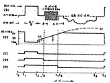
위상검출기(50), 보유 캐패시터(54) 및 타이밍회로(60)의 상세한 작동은 제2도의 파형을 참조하여 검토될 것이다. 파형(201)은 한수평주사 간격동안 가산회로(40)의 출력에서 발생된 NTSC 합성비데오 출력신호를 도시하고, 파형(202)는 노드 A전압을 도시한다(. 파형(203)은 동기검출기(Q1) 출력신호를 도시한다(고레벨은 콜렉터 전류흐름을 나타낸다). 파형(204 및 205)은 각각 비교기(64 및 62)에 의해 발생된 출력신호를 나타낸다(각각에 대해, 고레벨은 구동출력신호 레벨을 나타내고 저레벨은 억제출력신호 레벨을 나타낸다).The detailed operation of the
시간 t1에서 합성비데오 신호레벨은(파형(201)) 소거레벨에서 최대레벨로 전이되게 하고 연속적으로(시간 t2) 소거레벨로 그 반대의 전이를 시킨다. 시간간격(t1t2)는 합성비데오 신호의 동기 팁간격(NTSC 표준의 약 4.7㎲)에 상응하고, 타이밍회로(60)를 동기화 시키도록 동기분리기 트랜지스터 Q1에 의해 검출된다. 검출은 디엠파시스 회로(36)의 출력에서 발생된 NTSC 휘도신호(도시치 않음)의 소거 및 최대신호 레벨 전압 중간이 될 기준전압 V1의 값 선택에 의해 제공된다. 휘도신호는 Q1의 에미터에 인가되므로, 이것의 베이스 에미터 접합은 순바이어스되고 콜렉터 전류는 파형(203)으로 도시된 바와같이 동기 팁간격을 통하는 동안 내내 흐른다.At time t 1 , the composite video signal level (waveform 201) causes the transition from the erase level to the maximum level and the transition to the erase level continuously (time t 2 ) and vice versa. The time interval t 1 t 2 corresponds to the sync tip interval (about 4.7 ms of NTSC standard) of the composite video signal and is detected by the sync separator transistor Q1 to synchronize the
합성신호보다 휘도신호의 동기팁간격 검출에 의한 타이밍회로(60)의 동기화는(1) 동기분리기 트랜지스터 Q1의 트리거링 또는 오검출을 방지하는 장점과 (2)전압 V1의 조절 또는 정밀한 조정 필요성을 제거하는 등의 2가지 장점을 제공한다. 설명을 위해, Q1의 에미터는 가산회로(40)의 출력에 접속되었다고 가정한다. 동기팁을 확실히 검출하도록 칼라버스트 신호의 피크 및 동기팁 중간이될 V1 선택이 필수적이고, 다른 방법으로 Q1은 칼라버스트 신호에 의해 칼라버스트 간격동안 잘못 트리거될 수 있다(버스트의 피크는 통상적으로 동기팁 높이의 반이다). 이 가능한 난점은, 칼라버스트가 콤여파에 의해 휘도신호로부터 유효하게 제거되므로 트랜지스터Q1의 에이터에 비데오 출력신호의 휘도성분을 인가시키는데 의해 방지된다.Synchronization of the
본 발명의 동기화 회로의 다른 장점은 이것이 접적형태로 구성될 수 있는 점이다. 필요한 모든 것은 공통베이스 접속 트랜지스터 또는 어떤 다른 형태의 비교기에 적절히 접속된다. 동기 검출로서 칼라버스트 간섭을 방지하도록 통상적으로 "링" 또는 공진회로를 사용하는 텔레비죤 수상기의 동기검출 회로망이 이것과 비교된다. 이러한 해결법의 단점은 공진회로가 집적회로 구조에 대한 소자로 실행되지 않고 값이 비싸고 용적이 큰 인덕터 및 캐패시터가 요구되는 점이다.Another advantage of the synchronization circuit of the present invention is that it can be configured in a contact form. All that is needed is properly connected to a common base connected transistor or some other type of comparator. The synchronization detection network of a television receiver, which typically uses a "ring" or resonant circuit, is compared to this to prevent color burst interference as synchronization detection. A disadvantage of this solution is that the resonant circuit is not implemented as an element for the integrated circuit structure and requires expensive and bulky inductors and capacitors.
램프 크램프 트랜지스터 Q2는 트랜지스터 Q1에 의해 제공된 콜렉터 전류에 반응하여 동기팁 간격(t1-t2)동안 턴온되고 한 반도체 접합 전압강하(파형(202)의 Vbe)의 전압레벨로 적분 캐패시터 C1을 방전시킨다. 이 결과는 반포화 다이오드 D1 및 D2가 트랜지스터 Q2의 콜렉터 및 베이스 전압과 동일해지는 경향이 있기 때문이며 그에 의해 이것의 재생(턴오프) 시간을 증강시키며 포화를 방지한다. 이것은 타이밍회로(60)에 의해 발생된 시간간격이 Q2의 포화저장 시간에 좌우되지 않는것을 보장하는 본 발명의 특징을 나타낸다. (저장시간은 가변이고 비교적 예기할 수 없는 변수이다).Lamp clamp transistor Q2 is turned on during the sync tip interval t 1 -t 2 in response to the collector current provided by transistor Q1 and discharges the integral capacitor C1 to the voltage level of one semiconductor junction voltage drop (Vbe of waveform 202). Let's do it. This result is because half-saturated diodes D1 and D2 tend to be the same as the collector and base voltages of transistor Q2, thereby enhancing its regeneration (turn-off) time and preventing saturation. This represents a feature of the present invention that ensures that the time interval generated by the
저항 R3는 Q2의 포화방지 보조의 기능과 이것의 턴오프 시간을 증강시키는 두 기능을 제공한다. 다이옥드 D1및 D2는 Q2의 콜렉터 및 베이스 전압에 동일하게 되는 경향이 있음을 상기하자. 동등화는 다이오드가 동일한 접합구역이거나 동일한 전류레벨을 실행할 경우, 정확하게 될것이다. 저항 R3없이 다이오드 D1의 전류레벨은(캐패시터 C1이 방전된 후) Q2의 직류공통 에미터 전류이득(하이브리드 변수 기호법의 hFE)에 동일한 계수에 의해 다이오드 D2의 전류레벨보다 크다. 따라서, 한개는 이것의 베이스 전압보다 작은 것으로부터 Q1의 콜렉터 전압을 방지하도록 두 가지 선택을 가진다. 예를들면, 한개는 hFE와 동일하도록 D1및 D2의 접합구역비를 선택할수 있다. 그러나, 이러한 시도의 단점은 한 다이오드가 다른 것에 비해 매우 커야되는 점이다. 도시된 바와같이, Q2의 베이스-에미터 접합 양단에 저항 R3를 접속시키는 다른 선택은 작아질(예를들면, 단일로) 접합구역비를 허용하는 다이오드 D2에 부가전류를 제공한다. 더우기, 턴오프시간은 저항 R3에 의해 향상되는데, 이는 트랜지스터 Q1이 턴오프될때 Q2의 베이스에 턴오프 바이어스를 제공하기 때문이다.Resistor R 3 provides two functions, Q2's anti-saturation aid and augment its turn-off time. Recall that diodes D 1 and D 2 tend to be equal to the collector and base voltage of Q 2 . Equalization will be accurate if the diodes are running at the same junction area or at the same current level. The current level of diode D 1 without resistor R 3 (after capacitor C 1 is discharged) is greater than the current level of diode D 2 by a factor equal to the DC common emitter current gain of Q 2 (hFE of hybrid variable notation). Thus, one has two choices to prevent the collector voltage of Q 1 from being less than its base voltage. For example, one can choose the junction ratio of D 1 and D 2 to be equal to hFE. However, a disadvantage of this approach is that one diode must be very large compared to the other. As shown, another option to connect resistor R 3 across the base-emitter junction of Q 2 provides additional current to diode D 2 which allows for a smaller junction area ratio (eg, singly). Moreover, the turn-off time is improved by the resistor R 3 because it provides a turn-off bias to the base of Q 2 when transistor Q 1 is turned off.
시간 t2에서, 트랜지스터 Q1및 Q2가 턴오프될때, 노드 A 전압단계(파형(202)가)발생한다. 이 단계의 진폭 Δv는 제어가능한 변수이고 등식 y=mx+Δv+b…(1)로부터 산정되는 램프전압 y를 발생시키도록 적분 캐패시터 전압에 부가되는 일정한 오프셋트 전압을 나타낸다. 여기에서, y는 노드 A전압이고 m은 캐패시터 C1의 전압의 변화비이고, x는 시간이고, b는 C1의 최초 전압이며, Δv는 오프셋트(단계)전압이다.At time t 2 , when transistors Q 1 and Q 2 are turned off, a node A voltage step (waveform 202) occurs. The amplitude Δv at this stage is a controllable variable and the equation y = mx + Δv + b... The constant offset voltage added to the integrated capacitor voltage to generate the ramp voltage y calculated from (1) is shown. Here, y is the node A voltage, m is the change ratio of the voltage of capacitor C 1 , x is time, b is the initial voltage of C 1 , and Δv is the offset (step) voltage.
본 발명의 특징은 위상검출기(50) 및 예비충전회로(58)에 공급된 신호의 타이밍이 림프경사 m과 오프셋트 전압 Δv의 선택에 의해 제어될수 있는 것이고, 이들 변수는 독립적으로 제어된다. 연속적으로 설명되어질 바와같이 경사 m은 위상로크 "창" (간격 t3-t4)의 폭을 제어하고, 오프셋트 Δv는 수평동기신호의 후방포치(t2-t5)를 따라 창의 위치를 제어한다.A feature of the present invention is that the timing of the signals supplied to the
더욱 상세하게, 시간 t2에서 트랜지스터 Q1및 Q2가 턴오프될때, 캐패시터 C1은 Vbe 볼트의 전압레벨(등식(1)의 b항)로 충전될 것이다. 캐패시터 C1의 전압은 이것에 공급된 충전전류 및 C1의 값에 비례하는 최초비 m에서 변화되도록 즉시 개시될 것이다. 저항 R2의 값보다 매우 더 큰 저항 R1의 값을 선택하는데 의해(또는 정전류원으로 저항R1을 대치시키는데 의해), 충전전류 및 경사 m은 저항 R2의 값에 무관하게 제작될수 있다. 그러나, 충전전류는 저항 R2를 통해 흐르므로, 오프셋트 전압 Δv는 그것의 양단에서 발생되고, 저항 R2는 캐패시터 C1과 직렬이므로, 오프셋트 전압은 캐패시터 전압에 부과된다. 따라서, 램프경사 및 창폭을 결정하는 주어진 충전전류에 대한 저항 R2의 값은 램프 오프셋트와 창위치를 제어하도록 독립적으로 변화될수 있다.More specifically, when transistors Q 1 and Q 2 are turned off at time t 2 , capacitor C 1 will charge to the voltage level of Vbe volts (b term of equation (1)). The voltage of capacitor C 1 will be immediately started to change at an initial ratio m proportional to the charge current supplied thereto and the value of C 1 . By selecting the value of the resistor R 1 which is much larger than the value of the resistor R 2 (or by replacing the resistor R 1 with a constant current source), the charging current and the slope m can be made irrespective of the value of the resistor R 2 . However, since the charging current flows through the resistor R 2 , the offset voltage Δv is generated at both ends thereof, and since the resistor R 2 is in series with the capacitor C 1 , the offset voltage is imposed on the capacitor voltage. Thus, the value of the resistor R 2 for a given charging current that determines the ramp slope and window width can be changed independently to control the lamp offset and window position.
간격(t2t5)동안, 노드 A전압은 램프제한 트랜지스터Q3의 Vbe와 기준전압 V3의 합에 동일한 제한치로 선형증가하고 그때 트랜지스터 Q3는 어떤 또 다른 증가를 방지하도록 턴온된다. 트랜지스터 Q3는 수평간격의 잔여기간(t5-t7)동안 유지된다. 파형(202)의 램프전압의 연장된 점선은 램프전압이 제한되지 않고 기준전압 V2에 점차로 접근되는 것을 도시한다. 예정된 값으로 램프전압의 제한은 (1) C1을 방전하도록 트랜지스터 Q2에 요구되는 시간길이를 감소시키고 (2) 트랜지스터 Q2의 피크 콜렉터 전류흐름 및 베이스 전류 구동요구를 제한하는 장점을 제공한다.During the interval t 2 t 5 , the node A voltage increases linearly with a limit equal to the sum of Vbe and the reference voltage V 3 of the ramp limiting transistor Q 3 and then transistor Q 3 is turned on to prevent any further increase. Transistor Q 3 is maintained for the remaining period t 5 -t 7 of the horizontal interval. The extended dashed line of the ramp voltage of
파형(204)은 기준전압 V5와 노드 A 전압을 비교하는 비교기(64)에 의해 예비충전회로(58)에 공급된 제어신호를 나타낸다. 간격(t1-t3)동안, 램프전압은 V5이하이고 비교기(64)는 예비충전회로(58)에 구동신호를 공급한다. 램프전압이 V5를 초과할때, 비교기(58)는 예비충전회로 구동신호(t3-t7)를 중단한다.The
파형(205)은 기준전압 V4(V5보다 더 정극성인 도시된 바와같은 ΔV)와 노드 A전압을 비교하는 비교기(62)에 의해 위상검출기(50)에 공급된 제어신호를 나타낸다. 시간간격(t1-t4)동안, 램프전압은 V4이하이고 비교기(62)는 위상검출기(50)에 구동신호를 공급한다. 램프전압이 V4를 초과할때, 비교기(62)는 위상검출기 구동신호를 종료시킨다.
예비충전회로(58) 및 위상검출기(50)는 시간간격(t1-t3)동안 모두 구동됨이 주목될 것이다. 이것은 필수적이지는 않고 시간 t3까지 위상검출기(50)의 턴온을 지연시킬수 있다. 그것은, 예를들면, 비교기(64)가 예비충전회로(58)에 구동신호를 공급할때, 간격(t1-t3) 동안 비교기(62)의 출력을 억제시키기 위해 적절한 게이트 또는 제어회로망에 의해 실행될수 있다. 그러나, 이러한 변화는 부가적인 회로망을 요구하고 따라서 타이밍 신호발생의 복잡성 및 단가가 상승된다.It will be noted that the
간격(t1-t3) 동안, 예비충전회로(58)가 구동될때, 오차전압 보유캐패시터(54)는 서보장치 동적영역의 중심에 상응하는 전압레벨로 예비충전된다. 위상로크 손실이 발생되어야만 될 경우, 반복바이어스로 결합된 위상검출기(50)로부터 밀집 또는 일관된 신호의 부재는 궁극적으로 암스트레쳐 변환기(72)를 재중심시키는 경향이 있을 것이고 이것의 제어영역(5.11MHz)의 중심에서 VCO(42)를 위치시킬 것이다. 앞서 설명된 바와같이, 이것은 위상로크의 재습득이 발생되는 최적상태이다. 다른 한편, 서보가 위상 고정상태일 경우, 캐패시터(54)의 예비충전은 예비충전비(한번의 매주사간격)가 필터(56)의 주파수보다 매우 높기 때문에, 별 영향을 받지않을 것이고 반면에, 위상검출기 출력전압 변화비는(선대선 바이어스로 관측된) 필터 대역폭내이다.During the interval t 1 -t 3 , when the
Claims (1)
Applications Claiming Priority (2)
| Application Number | Priority Date | Filing Date | Title |
|---|---|---|---|
| US06/068,014 US4286282A (en) | 1979-08-20 | 1979-08-20 | Periodically biased video disc player servo system |
| US68014 | 1979-08-20 |
Publications (1)
| Publication Number | Publication Date |
|---|---|
| KR840000113B1 true KR840000113B1 (en) | 1984-02-11 |
Family
ID=22079874
Family Applications (1)
| Application Number | Title | Priority Date | Filing Date |
|---|---|---|---|
| KR1019800003254A KR840000113B1 (en) | 1979-08-20 | 1980-08-19 | Periodically biased video disc player servo system |
Country Status (8)
| Country | Link |
|---|---|
| US (1) | US4286282A (en) |
| JP (1) | JPS5644162A (en) |
| KR (1) | KR840000113B1 (en) |
| AT (1) | AT383925B (en) |
| DE (1) | DE3031467C2 (en) |
| FR (1) | FR2464002B1 (en) |
| GB (1) | GB2062382B (en) |
| IT (1) | IT1132347B (en) |
Families Citing this family (7)
| Publication number | Priority date | Publication date | Assignee | Title |
|---|---|---|---|---|
| US4360829A (en) * | 1980-06-24 | 1982-11-23 | Rca Corporation | Active distortion elimination circuitry for a video disc player |
| JPS57149970A (en) * | 1981-03-13 | 1982-09-16 | Victor Co Of Japan Ltd | Phase comparing circuit |
| US4520402A (en) * | 1982-11-15 | 1985-05-28 | Rca Corporation | Video apparatus with burst locked heterodyne chroma converter and residual time base error correction |
| JPS6151673A (en) * | 1984-08-21 | 1986-03-14 | Pioneer Electronic Corp | Time base control system |
| US6147597A (en) * | 1999-03-31 | 2000-11-14 | Facory; Omar | Vehicle-integrated access control device |
| KR100716954B1 (en) * | 2000-09-05 | 2007-05-14 | 삼성전자주식회사 | De-Emphasis circuit design method of video signal processing IC and IC using thereof |
| JP2011010053A (en) * | 2009-06-26 | 2011-01-13 | Hitachi-Lg Data Storage Inc | Device and method for detecting information |
Family Cites Families (10)
| Publication number | Priority date | Publication date | Assignee | Title |
|---|---|---|---|---|
| GB1267251A (en) * | 1968-04-23 | 1972-03-15 | ||
| US3629491A (en) * | 1969-11-03 | 1971-12-21 | Bell & Howell Co | Signal-correcting apparatus |
| GB1457407A (en) * | 1973-03-20 | 1976-12-01 | Rca Corp | Playback apparatus with speed correctionsystem |
| JPS5739598B2 (en) * | 1974-04-23 | 1982-08-21 | ||
| US3965482A (en) * | 1974-11-12 | 1976-06-22 | Rca Corporation | Velocity correction circuit for video discs |
| US3949418A (en) * | 1975-01-27 | 1976-04-06 | Gte Sylvania Incorporated | Burst gate and backporch clamping circuitry |
| JPS524889A (en) * | 1975-07-01 | 1977-01-14 | Toyo Kohan Co Ltd | Continuous selection circuit of automatic scar inspector |
| JPS5376620A (en) * | 1976-12-17 | 1978-07-07 | Sony Corp | Processing circuit for color video signal |
| JPS5831152B2 (en) * | 1977-10-17 | 1983-07-04 | ソニー株式会社 | Color video signal processing circuit |
| JPS5461414A (en) * | 1977-10-26 | 1979-05-17 | Toshiba Corp | Correction unit for time axis variation |
-
1979
- 1979-08-20 US US06/068,014 patent/US4286282A/en not_active Expired - Lifetime
-
1980
- 1980-08-07 IT IT24050/80A patent/IT1132347B/en active
- 1980-08-14 AT AT0418580A patent/AT383925B/en not_active IP Right Cessation
- 1980-08-15 GB GB8026786A patent/GB2062382B/en not_active Expired
- 1980-08-19 FR FR8018152A patent/FR2464002B1/en not_active Expired
- 1980-08-19 KR KR1019800003254A patent/KR840000113B1/en active
- 1980-08-20 DE DE3031467A patent/DE3031467C2/en not_active Expired
- 1980-08-20 JP JP11533280A patent/JPS5644162A/en active Granted
Also Published As
| Publication number | Publication date |
|---|---|
| IT1132347B (en) | 1986-07-02 |
| JPS6331156B2 (en) | 1988-06-22 |
| IT8024050A0 (en) | 1980-08-07 |
| JPS5644162A (en) | 1981-04-23 |
| AT383925B (en) | 1987-09-10 |
| DE3031467C2 (en) | 1982-12-30 |
| US4286282A (en) | 1981-08-25 |
| GB2062382A (en) | 1981-05-20 |
| FR2464002A1 (en) | 1981-02-27 |
| GB2062382B (en) | 1983-09-21 |
| ATA418580A (en) | 1987-01-15 |
| DE3031467A1 (en) | 1981-03-26 |
| FR2464002B1 (en) | 1985-11-08 |
Similar Documents
| Publication | Publication Date | Title |
|---|---|---|
| JPS6046596B2 (en) | squelch circuit | |
| KR840000113B1 (en) | Periodically biased video disc player servo system | |
| EP1605688A2 (en) | Signal processing device | |
| KR830000226B1 (en) | Video processing system with comb filter | |
| US4614981A (en) | Apparatus for reproducing video signal | |
| US4544943A (en) | Stabilized color television subcarrier regenerator circuit | |
| CA1154156A (en) | Nested loop video disc servo system | |
| KR920001064B1 (en) | Magnetic recording and reproducing apparatus | |
| US5323242A (en) | Carrier signal generating circuit in video signal recording/reproducing apparatus | |
| US4520402A (en) | Video apparatus with burst locked heterodyne chroma converter and residual time base error correction | |
| US4345279A (en) | Time base correction apparatus | |
| US5109285A (en) | Time base correction circuit for a reproduced video signal from a video tape recorder | |
| KR930010936B1 (en) | Jitter detecting circuit | |
| JPH0221198B2 (en) | ||
| KR790000849B1 (en) | Chrominance signal correction circuit | |
| JPH0634521B2 (en) | Magnetic recording / reproducing circuit | |
| JP2697070B2 (en) | Color signal processing device | |
| KR890000151Y1 (en) | Synchronizing signal generating circuit of hifi-vtr | |
| KR800000658B1 (en) | Sync responsive systems for video dise players | |
| GB2156629A (en) | Apparatus for the color synchronization of reproduced video signals | |
| JPS6111517B2 (en) | ||
| JPS6122378Y2 (en) | ||
| JPS62249592A (en) | Time base correcting device | |
| JPS5943695A (en) | Picture recorder and reproducer | |
| JPH0220992A (en) | Time base correcting circuit |