KR810000019B1 - Charge coupled imaging device - Google Patents
Charge coupled imaging device Download PDFInfo
- Publication number
- KR810000019B1 KR810000019B1 KR7200375A KR720000375A KR810000019B1 KR 810000019 B1 KR810000019 B1 KR 810000019B1 KR 7200375 A KR7200375 A KR 7200375A KR 720000375 A KR720000375 A KR 720000375A KR 810000019 B1 KR810000019 B1 KR 810000019B1
- Authority
- KR
- South Korea
- Prior art keywords
- charge
- electrodes
- storage medium
- array
- row
- Prior art date
Links
- 238000003384 imaging method Methods 0.000 title claims abstract description 5
- 238000003860 storage Methods 0.000 claims abstract description 17
- 239000002800 charge carrier Substances 0.000 claims abstract description 15
- 239000002184 metal Substances 0.000 claims description 14
- 238000009825 accumulation Methods 0.000 claims description 8
- 238000003491 array Methods 0.000 claims description 6
- 238000009413 insulation Methods 0.000 abstract 1
- 239000004065 semiconductor Substances 0.000 description 19
- 238000009792 diffusion process Methods 0.000 description 11
- 239000000463 material Substances 0.000 description 8
- 239000000969 carrier Substances 0.000 description 6
- 230000008878 coupling Effects 0.000 description 6
- 238000010168 coupling process Methods 0.000 description 6
- 238000005859 coupling reaction Methods 0.000 description 6
- 238000000034 method Methods 0.000 description 5
- 230000000712 assembly Effects 0.000 description 4
- 238000000429 assembly Methods 0.000 description 4
- 238000004519 manufacturing process Methods 0.000 description 4
- 239000012212 insulator Substances 0.000 description 3
- 230000008569 process Effects 0.000 description 3
- 230000006798 recombination Effects 0.000 description 3
- 238000005215 recombination Methods 0.000 description 3
- VYPSYNLAJGMNEJ-UHFFFAOYSA-N Silicium dioxide Chemical compound O=[Si]=O VYPSYNLAJGMNEJ-UHFFFAOYSA-N 0.000 description 2
- 238000004132 cross linking Methods 0.000 description 2
- 239000003989 dielectric material Substances 0.000 description 2
- 229910052710 silicon Inorganic materials 0.000 description 2
- 239000010703 silicon Substances 0.000 description 2
- 239000007787 solid Substances 0.000 description 2
- 206010034960 Photophobia Diseases 0.000 description 1
- 238000010521 absorption reaction Methods 0.000 description 1
- 230000002238 attenuated effect Effects 0.000 description 1
- 230000000903 blocking effect Effects 0.000 description 1
- 230000008859 change Effects 0.000 description 1
- 238000010924 continuous production Methods 0.000 description 1
- 230000002950 deficient Effects 0.000 description 1
- 238000010586 diagram Methods 0.000 description 1
- 238000010894 electron beam technology Methods 0.000 description 1
- 239000011810 insulating material Substances 0.000 description 1
- 208000013469 light sensitivity Diseases 0.000 description 1
- 230000004048 modification Effects 0.000 description 1
- 238000012986 modification Methods 0.000 description 1
- 230000003287 optical effect Effects 0.000 description 1
- 238000005036 potential barrier Methods 0.000 description 1
- 235000012239 silicon dioxide Nutrition 0.000 description 1
- 239000000377 silicon dioxide Substances 0.000 description 1
- 238000003892 spreading Methods 0.000 description 1
- 230000007480 spreading Effects 0.000 description 1
- 230000007704 transition Effects 0.000 description 1
Images


Classifications
-
- G—PHYSICS
- G11—INFORMATION STORAGE
- G11C—STATIC STORES
- G11C19/00—Digital stores in which the information is moved stepwise, e.g. shift registers
- G11C19/28—Digital stores in which the information is moved stepwise, e.g. shift registers using semiconductor elements
- G11C19/282—Digital stores in which the information is moved stepwise, e.g. shift registers using semiconductor elements with charge storage in a depletion layer, i.e. charge coupled devices [CCD]
-
- H—ELECTRICITY
- H01—ELECTRIC ELEMENTS
- H01L—SEMICONDUCTOR DEVICES NOT COVERED BY CLASS H10
- H01L27/00—Devices consisting of a plurality of semiconductor or other solid-state components formed in or on a common substrate
- H01L27/14—Devices consisting of a plurality of semiconductor or other solid-state components formed in or on a common substrate including semiconductor components sensitive to infrared radiation, light, electromagnetic radiation of shorter wavelength or corpuscular radiation and specially adapted either for the conversion of the energy of such radiation into electrical energy or for the control of electrical energy by such radiation
- H01L27/144—Devices controlled by radiation
- H01L27/146—Imager structures
- H01L27/148—Charge coupled imagers
- H01L27/14831—Area CCD imagers
Landscapes
- Physics & Mathematics (AREA)
- Engineering & Computer Science (AREA)
- Power Engineering (AREA)
- Electromagnetism (AREA)
- Condensed Matter Physics & Semiconductors (AREA)
- General Physics & Mathematics (AREA)
- Computer Hardware Design (AREA)
- Microelectronics & Electronic Packaging (AREA)
- Solid State Image Pick-Up Elements (AREA)
- Transforming Light Signals Into Electric Signals (AREA)
Abstract
Description
제1a도 내지 제1c도는 본 소자의 작동을 실증하는 본 발명의 한 실시예에 따른 면영상소자내의 전극의 한 종렬을 도시한 개략도.1A to 1C are schematic diagrams showing one column of electrodes in a planar image device according to one embodiment of the present invention demonstrating the operation of the device.
제2도는 본 발명의 실시예에 따른 면영상소자의 개략적인 평면도.2 is a schematic plan view of a planar image device according to an embodiment of the present invention.
제3도는 제2도의 선 3-3'를 따라 절단한 면영상소자의 단면도.3 is a cross-sectional view of the planar image device cut along the line 3-3 ′ of FIG. 2.
제4도는 본 발명의 다른 실시에 따른 선영상소자의 평면도.4 is a plan view of a line image device according to another embodiment of the present invention.
본 발명은 고상(固狀)면 및 선 영상 소자에 관한 것이다.TECHNICAL FIELD This invention relates to a solid-state surface and a line image element.
현재 주사(走査)요소로서 전자비임(beam)을 이용하고 있는 소자를 대치시켜서 고상으로 된 면영상소자와 선영상소자를 개발하기 위하여 다각도로 시도를 하고 있다. 최근에, 두 가지의 신형의 반도체정보축적 소자가 제안되어, 이러한 영상소자를 경제적으로 제조할 수 있게 되었다.At present, attempts are being made at various angles to develop a planar image device and a line image device having a solid state by replacing an element using an electron beam as a scanning element. Recently, two new types of semiconductor information accumulating elements have been proposed, which makes it possible to manufacture such image elements economically.
이 정보축적소자의 한 형태는 전하결합소자(CCD)로 알려져 있다(예를 들어, 응용물리학논문 제3호, 17권, 111-115페이지에 있는 톰프셋씨 등이 쓴 "전하결합 8-비트전이레지스터" 참조). 이 소자는 반도체 매체의 한 표면 위에 놓인 절연층에 따라 배치된 금속전극배열을 포함한다. 이 소자는 바이어스된 전극밑에 생긴 전위우물 내에 매체내의 이동성전하캐리어를 축적하고 일련의 전극들이 연속적으로 바이어스될 때 반도체 표면을 따라 연속적인 전위 우물을 만들므로서 전하를 이송한다. 전하캐리어는 여러가지 방법으로 생길 수 있다. 한 방법은 광자흡수에 의해 매치 내에서 정공-전자쌍을 발생시키는 것이다. 이때 소수캐리어는 입사광에 비례하여 바이어스된 전극의 영향에 의해 형성된 전위우물 속으로 퍼지고 적당한 일련의 전극을 연속적으로 바어어싱하므로서 간단하게 해독될 수 있다(1971년 11월 9일부로 연속출원된 미합중국 특허원 제196,933호의 미합중국 특허 제3,858,232호를 위해 표기된 더블류. 에스. 보일과 지. 이. 스미스가 1970년 2월 16일부로 출원한 미합중국특허원 제11,541호 참조).One form of this information accumulating element is known as a charge-coupled element (CCD) (e.g., a charge-coupled 8-bit writer written by Tomsset et al. In Applied Physics, Vol. See Transition Register). The device includes an array of metal electrodes disposed along an insulating layer overlying one surface of a semiconductor medium. This device transfers charge by accumulating mobile charge carriers in the medium within the potential wells underneath the biased electrodes and creating a continuous potential well along the semiconductor surface when a series of electrodes are continuously biased. Charge carriers can occur in several ways. One method is to generate hole-electron pairs in a match by photon absorption. At this time, the minority carrier can be easily decoded by spreading into a potential well formed by the influence of the electrode biased in proportion to the incident light and by sequentially balancing the appropriate series of electrodes (US patent filed consecutively on November 9, 1971). See US Patent No. 11,541, filed February 16, 1970, by S. Boyle and G. Smith, for US Patent No. 3,858,232 to US Pat.
영상을 응용하기 위해 사용될 수 있는 다른 형태의 정보축적소자는 부켓브리게이드소자(Bucket Brigade Device : BBD)로 알려져 있다(앤. 버그룬드와 애취. 제이 볼이 1970년 2훨 16일에 출원하여 1972년 5월 2일에 허여된 미합중국특허 제3,660,697호 참조). 이 소자는 또한 반도체매체 위에 있는 절연층상에 배치된 전극배열을 사용한다. 그러나, 확산영역은 각각의 전극밑의 반도체 내에 제공되어 전하이송통로 내의 인접전극 이하의 영역속으로 약간 연장된다. 전극이 펄스화되면, 확산은 즉시 역바이어스되고 이 확산과 이것의 부근에 있는 확산 사이의 채널은 반전된다. 그러므로, 전하는 소수캐리어와 같이 입사광에 비례하여 확산영역내에 모여서 축적되고 전극이 연속적으로 바이어스될 때 소수캐리어와 같이 확산 사이의 채널영역을 통하여 이송된다. 그러므로 역바이어스된 확산영역은 전하를 모으는 동안 CCD의 전위우물과 같은 방법으로 형성된다는 것을 쉽게 알 수 있다.Another type of information storage device that can be used for imaging is known as the Bucket Brigade Device (BBD) (An. Berglund and Ache. See US Patent No. 3,660,697, issued May 2, 2008). The device also uses an array of electrodes disposed on an insulating layer over the semiconductor medium. However, the diffusion region is provided in the semiconductor under each electrode and extends slightly into the region below the adjacent electrode in the charge transfer path. When the electrode is pulsed, the diffusion is immediately reverse biased and the channel between this diffusion and the diffusion in its vicinity is reversed. Therefore, the charge is collected and accumulated in the diffusion region in proportion to the incident light like the minority carrier, and is transferred through the channel region between the diffusion like the minority carrier when the electrodes are continuously biased. Therefore, it can be easily seen that the reverse biased diffusion region is formed in the same way as the potential well of the CCD while collecting charge.
제안된 이 소자들에 관련된 결점중의 하나는 선명도가 좋지 않다는 것이다. 즉, 빛이 매체상에 연속적으로 입사되기 때문에, 부수적인 캐리어가 해독하는 동안 모여져서 영상을 약하게 한다. CCD와 BBD소자는 적당하게 바이어스된 전극들에 의해 반도체매체내에 전하캐리어를 축적하고 이송시키기 때문에, "전하 이송 소자(CTD)"란 말은 두 소자형태의 일반적인 용어로 되었다. "국부적인 집적단" 이란 말은 CCD의 전위우물이나 BBD의 등가확산영역인 전하수집영역이란 용어로 쓰인다.One of the drawbacks associated with these proposed devices is their poor clarity. That is, because light is continuously incident on the medium, incidental carriers gather during decoding and weaken the image. Since CCD and BBD devices accumulate and transport charge carriers in a semiconductor medium by suitably biased electrodes, the term “charge transfer device (CTD)” has become a general term for both device types. The term "local integrated stage" is used as the term "potential well" of a CCD or "charge collection area", an equivalent diffusion region of a BBD.
따라서 본 발명의 주 목적은 제조하기에 간단하고, 광감도가 높으며 전하결합소자에 관련된 영상손상문제를 극복한 영상소자를 제조하는 것이다.Accordingly, a main object of the present invention is to manufacture an image device that is simple to manufacture, has high light sensitivity, and overcomes an image damage problem associated with a charge coupled device.
본 발명에 따르면, 전하축적매체, 상기 매체의 한 표면의 최소한 일부를 덮고 있는 절연층, 상기 절연층 상에 형성된 제1금속전극배열, 이 제1배열내에 전하캐리어를 형성하도록 상기 축적매체의 한 표면상에 영상을 투사하기 위한 장치, 상기 매체상에 입사하는 빛에 비례하여 전극 아래의 상기 축적매체내에 전하 캐리어를 모으기 위하여 상기 제1전극배열을 바이어싱하기 위한 장치, 제1배열에 연속하여 축적매체의 면위의 상기 절연층상에 형성된 제2금속전극배열, 상기 제2배열을 상기 입사광으로부터 차단하기 위한 장치, 상기 제1배열 아래에서부터 상기 제2배열 아래까지 전하캐리어를 이송하도록 상기 제1 및 제2배열의 전극들을 연속적으로 바이어싱하기 위한 장치, 상기 제2배열의 전극을 아래의 축적매체내에 전하캐리어를 축적하도록 상기 제2배열을 바이어싱하기 위한 장치, 및 제2배열을 통하여 이송된 축적된 전하캐리어를 해독하기 위한 장치들을 포함하는 고상(固狀) 영상소자가 제공된다.According to the present invention, there is provided a charge storage medium, an insulating layer covering at least a portion of one surface of the medium, a first metal electrode array formed on the insulating layer, one of the accumulation medium to form a charge carrier in the first array. Apparatus for projecting an image onto a surface, Apparatus for biasing the first electrode array to collect charge carriers in the accumulation medium under an electrode in proportion to light incident on the medium, continuously in a first array A second metal electrode array formed on the insulating layer on the surface of the storage medium, a device for shielding the second array from the incident light, the first and second carriers to transfer charge carriers from below the first array to below the second array; An apparatus for continuously biasing electrodes of a second array, the second array of electrodes for accumulating charge carriers in a storage medium below the second array of electrodes; A solid state imaging device is provided that includes a device for biasing an array and a device for decoding the accumulated charge carriers transferred through the second array.
그러므로 본 발명은 감광배열과 축적 및 해독배열로 작용하는 두개의 MIS 소자배열을 포함할 수 있다는 것을 이해할 수 있다. 전하캐리어는 입사광에 비례하여 감광배열의 금속전극 밑의 전위우물내에 형성된다. 이 정보는 어떠한 빛과도 차폐되어 있는 축적 및 해독 배열의 전극들 밑의 영역으로 신속하게 이송 된다. 이때 이 정보는 광학정보를 손상시키지 않고 축적 및 해독배열로부터 해독될 수 있다. 이 소자내에는 횡결합을 방지하고 이송하는 동안 이송효율을 일정하게 유지하기 위한 장치가 포함되어 있다.Therefore, it will be appreciated that the present invention may include two MIS device arrays that act as photosensitive arrays and accumulation and readout arrays. The charge carriers are formed in the potential well under the metal electrode of the photosensitive array in proportion to the incident light. This information is quickly transferred to the area underneath the electrodes in the accumulation and readout arrangement that is shielded from any light. This information can then be decoded from the accumulation and decryption arrangement without damaging the optical information. Within this device, a device is included to prevent lateral coupling and to maintain a constant transfer efficiency during transfer.
이하 첨부된 도면을 참조하여 본 발명을 더욱 상세하게 기술하겠다.Hereinafter, the present invention will be described in more detail with reference to the accompanying drawings.
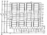
제1a도 내지 제1c도는 면영상소자의 기본 구조와 동작을 도시한 것이고, 제2도는 전체 배열의 평면도이다. 간단하게 하기 위하여, 소자는 행으로 4부재, 열로 6부재의 감광배열을 갖는 것으로 도시되어 있다. 본 발명의 원리는 더 큰 배열로 확장될 수 있다.1A to 1C show the basic structure and operation of the surface image element, and FIG. 2 is a plan view of the entire arrangement. For simplicity, the device is shown having a photosensitive array of four members in a row and six members in a row. The principles of the present invention can be extended to larger arrangements.
특히 제1a도를 참조하면, 소자는 n형 실리콘일 수도 있는 반도체 용적부분(10)을 포함한다. 이 용적의 표면 위에는 예를 들어 이산화실리콘일 수도 있는 유전층(11)이 있다. 이 유전층의 상부위에는 일련의 금속전극 12a-d, 13a-d, 14a-d 및 15가 있다. 이 전극들은 제1a도에 도시한 바와 같이 면영상소자내에 1종렬의 MIS소자를 형성 한다.In particular with reference to FIG. 1A, the device includes a
(30)과 같은 물체의 영상은 광원(16)과 렌즈(29)에 의해 전극반대편의 반도체용적의 표면 위에 투사된다. 이 표면의 일부는 불투명시계(視界) 조리계(17)과 같은 장치에 의해 빛과 차단된다. 빛을 차단하기 위해 사용되는 장치는 중요하지 않다. 그러므로, 소자는 두 부분으로 나누어 생각될 수도 있다. 제1의 6개 전극은 1종렬의 면감광배열을 형성하고, 제2의 7개 전극은 다음에 상세하게 기술되는 바와 같이 한 종렬의 면축적 및 해독배열을 형성한다. 영상은 투면전극이 갖추어질 수 있기 때문에 반도체용적의 전극측 면상에 투사될 수 있다는 것을 주지해야 한다.An image of an object such as 30 is projected on the surface of the semiconductor volume opposite the electrode by the
감광부분내에서, 3상전하결합장치를 형성하도록 전극(12a)와 (12b)는 도전통로 A1에 결합되고, 전극(13a)와 (13b)는 도전통로 A2에 결합되며, 전극(14a)와 (14b)는 도전통로 A3에 결합된다. 이와 마찬가지로, 모든 축적 및 해독배열 부분의 3전극은 도전통로 C1에 결합된 전극(15)을 제외하고는 도전통로 B1, B2또는 B3중의 하나에 결합된다. 크럭(Clock) 펄스들은 다음에 설명되는 바와 같이 전극들을 연속적으로 바이어스하기 위하여 이 도전통로들에 각각 공급된다. 두 부분들의 대응전극들(예, 12a, 12b, 12c, 12d)이 시간내에 어떤 점에서 동시에 펄스화되도록 하기 위한 장치도 제공된다. 이 장치는 제1a도에 스위치 18, 19 및 20으로 개략적으로 도시되어 있다. 또한, 전하 정보를 해독하기 위하여, 도전통로 C1을 도전통로 B1에 결합시키기 위한 장치로 제공되는데, 이것은 스위치(21)로 도시되어 있다.In the photosensitive portion, the
소자의 동작은 우선 제1a도 내지 제1c도에 도시한 연속적인 과정을 참조하므로서 알 수 있다. 제1a도에서, 펄스는 전극들 밑의 반도체재료(10) 내에 전위우물을 형성하도록 도전통로 A2로부터 전극(13a) 와 (13b)에 인가되었다. 반도체재료에 입사된 빛은 반도체재료 내부에 정공-전자쌍을 발생시키고, 이때 소수캐리어는 가장 근접한 전위가 최소로 되도록 확산한다. 그러므로 각각의 전위우물내로 집결되고 도면에 "+"로 표시된 소수캐리어는 3전극들(12a,13a,14a 및 12b,13b,14b)로 된 각각의 셋트에 의해 덮힌 영역위의 반도체 표면의 빛의 세기를 측정한다.The operation of the device can be seen by first referring to the continuous process shown in FIGS. 1A to 1C. In FIG. 1A, a pulse was applied from the conductive passages A 2 to the
전하결합개념에 따르면, 이러한 전하집합체는 전극들을 연속적으로 펄스하므로서 반도체를 통해 이동될 수 있으므로, 반도체내에 전하가 흐를 연속적인 전위우물을 형성한다. 그러므로, 소자의 감광부분과 축적 -해독부분의 대응도전통로는 함께 결합되고, 펄스는 전하를 감광부분으로부터 축적-해독부분으로 신속하게 이동시키기 위해서 빠른 속도로 연속적으로, A1,A2및 A3에 인가된다. 제1b도에 도시한 과정에서, 전하집합체는 전극(13C)와 (13d) 밑에 억류되어 있다. 신속한 이동은 심각한 손상작용을 방지하고, 축적 -해독부분이 빛과 차단되기 때문에, 전하는 소수캐리어를 부수적으로 모으지 않아도 느린 속도로 해독될 수 있다.According to the charge coupling concept, such a charge assembly can be moved through a semiconductor by continuously pulsed electrodes, thereby forming a continuous potential well through which charge flows in the semiconductor. Therefore, the corresponding conduction paths of the photosensitive and accumulation-decoding sections of the device are coupled together, and the pulses are continuously connected at high speeds A 1 , A 2 and A to quickly move charges from the photosensitive section to the accumulation-decoding sections. Is applied to 3 . In the process shown in FIG. 1B, the charge collector is held under the
축적-해독 부분으로부터 정보를 해독하기 위하여, 감광부분과 축적-해독 부분의 도전통로는 감결합된다. 이것은 감광부분이 계속 모이는 동안 축적-해독 부분에 있는 정보가 해독 되도록 도전통로 A2가 펄스된 채로 남아 있는 동안 도전통로 B1,B2, 및 B3가 펄스되게 한다. 해독 동작을 할때, 도전통로 C1은 전하가 최종전극(즉, 15)밑의 영역으로 이송되도록 스위치(21)을 폐쇄시키므로서 B1에 결합되어야 한다. 제1c도에 도시한 과정에서, 도전통로들은 제 1 전하집합체가 전극 (15)밑의 영역으로 이송되고, 제 2전하 집합체는 전극 (136)밑에 있게 되도록 B3-B1-B2의 순서로 펄스되었다. 제 1전하집합체는 전극(15)가 일련의 해독 배열의 한 전극을 나타내기 때문에 지면을 뚫고 나오는 방향이나 들어가는 방향으조 해독될수 있다. 이것은 제 2도를 참조하여 다음에 기술된다. 제 2전하 집합체는 동일한 펄스 및 해독의 순서에 의해 전극(15)로 연속적으로 이송될 수 있다. 이동안 감광배열은 전극 (13a)해 (13b)밑으로 전하를 계속 모으며, 이송 및 해독 과정이 반복된다.In order to decode the information from the accumulation-decoding portion, the conductive paths of the photosensitive portion and the accumulation-decoding portion are decoupled. This causes the conductive passages B 1 , B 2 , and B 3 to pulse while the conductive passage A 2 remains pulsed so that the information in the accumulation-decryption portion is decoded while the photosensitive portion continues to gather. In the deciphering operation, the conductive path C 1 must be coupled to B 1 by closing the
제2도는 제1a도 내지 제1c도에 도시한 4종렬의 소자에 의해 형성된 전체영역배열을 도시한 것이다. 즉, 제1c도 내지 제1c도의 각 전극들은 도전통로들 중의 하나에 공통으로 결함된, 4부재의 횡렬의 일부를 형성한다. 도면에서, 횡렬에 있는 전극들간의 상호접속은 본 소자의 기본구조를 설명하기 위하여 부분적으로 절단 되 었다.FIG. 2 shows the entire area array formed by the four rows of elements shown in FIGS. 1A to 1C. That is, each of the electrodes in FIGS. 1C-1C forms part of the four member row, which is commonly defective in one of the conductive passages. In the figure, the interconnections between the electrodes in the row were partially cut to illustrate the basic structure of the device.
도전통로 A2가 펄스될 때, 전하는 감광배열의 제2 및 제 5횡렬에 있는 전극들 밑으로 모이게 된다. 이 때, 이미 기술한 방법으로 전극들을 펄싱하므로서, 전하는 도전통로 B2에 결합된 횡렬의 축적전극들 밑의 영역으로 이송되고 연속적으로 한 라인을 한번에 해독한다. 해독 동작은 이미 언급한 전극(15)가 그 일부를 형성하는 횡렬전극들(22)에 의해 실시된다. 한 횡렬의 전하집합체들은 도전통로 B1,B2, 및 B3를 펄싱하므로서 이 최종 횡렬전극들 밑의 영역내로 이송되고 도전통로 C1은 스위치(21)을 통해 도전통로 B1에 결합된다. C1을 감결합한 후, 이 최종횡렬도전통로 들은 확산 P형 반도체 재료(23)의 영역과 같은 출력단 내로 측방향으로 전하를 이동시키기 위해서 C2-C3-C1의 순서로 펄스된다.When conductive path A 2 is pulsed, charge is collected under the electrodes in the second and fifth rows of the photosensitive array. At this time, by pulsing the electrodes in the manner described above, the charge is transferred to the area under the accumulating electrodes of the row coupled to the conductive path B 2 , and successively deciphers one line at a time. The readout operation is performed by the
이 출렬단 영역에 있는 전하는 이미 공지된 여러 방법으로 검출될 수 있다. 그러므로 본 소자의 동작은 연속적인 해독을 하기 위하여 이 출력단영역으로 전하를 형행하게 이송 한다고 일반적으로 기술될 수 있다.Charges in this column region can be detected in a variety of known ways. Therefore, the operation of the device can generally be described as transferring the charge to this output end region in order to perform continuous readout.
전하는 한번에 한 횡렬씩 반도체를 통하여 이송되기 때문에, 한 종렬전극들로부터 다음의 전극들로 전하가 결합하지 못하게 하고 가능한한 조밀하게 전극들을 배열하는 장치를 제공하는 것이 바람직하다. 제2도를 참조하면, 이것은 본 소자의 가장자리에 있는 유전물질위와 종렬 전극들 사이의 영역내에 금속스트립(strip)(24)를 제공 하므로서 이루어진다. 이 구조의 기능은 제3도의 선 3-3'를 따라 절단한 단면도인 제3도를 참조 하므로서 더욱 쉽게 이해될 수 있다.Since charges are transported through the semiconductor one row at a time, it is desirable to provide a device that prevents charge from coupling from one column electrode to the next and arranges the electrodes as densely as possible. Referring to Figure 2, this is done by providing a
제3도 내의 횡렬 전극들은 펄스 "ON"되어 있고, 소수 케리어는 용적밑의 역으로 이송된다. 금속스트립(24)는 펄스된 전극들에 의해 형성된 것보다 훨씬 얕은 용적재료내에 공핍영역을 형성하도록 일정한 부(-) 바이어스로 유지된다. 이것은 인접종렬 내로 전하가 이동되지 못하게 하도록 횡렬에 있는 각 전극들 밑에 존재하는 전하집합체간에 전위장벽이 생기게 한다.The row electrodes in FIG. 3 are pulsed ON and the minority carriers are transported inversely under the volume. The
바이어스된 금속스트립은 이송효율을 일정하게 유지하는 다른 기능을 수행한다. 실제로, 전극들이 펄스 되지 않을 때, 용적내에 얕은 공핍영역을 유지하기 위하여 모든 전극들에 균일한 바이어스를 인간하는 것이 바람직하다. 이것은 용적-유전체 내면에서 억류된 전하가 재결합하지 못하게 하기 위한 것이다.The biased metal strips perform another function of keeping the transfer efficiency constant. Indeed, when the electrodes are not pulsed, it is desirable to have a uniform bias on all the electrodes in order to maintain a shallow depletion region in the volume. This is to prevent charges held back inside the volume-dielectric from recombining.
그러나, 잔여전위에 형성된 공핍영역이 전극들 바로 밑의 영역으로 정해지기 때문에, 각 전극들의 연부 바로 다음 영역내에서는 전하재결합이 계속 발생하게 된다. 기술한 영상소자에서, 이와같은 재결합은 미소영역전극에 대해 현저해지는 전하 손실과 약한 이송효율을 야기시킨다. 그러므로, 금속스트립에 의해 이 연부 영역내에 형성된 공핍영역은 이와같은 바람직하지 못한 재결합을 방지한다.However, since the depletion region formed at the residual potential is defined as the region immediately below the electrodes, charge recombination continues to occur in the region immediately after the edges of the respective electrodes. In the imager described, such recombination results in a noticeable charge loss and weak transfer efficiency for the microregion electrode. Therefore, the depletion region formed in this edge region by the metal strip prevents such undesirable recombination.
제3도는 영상소자내에 한 횡렬전극들을 형성하기 위한 기술을 도시한 것이다. 금속스트립(24)간 유전체 표면 위에 형성된 후, 유전물질(25)는 그 스트립 위에 피착된다. 이때, 도전통로들중의 하나에 (제3도에 도시한 횡렬에서는 B2에) 횡렬전극들이 결합되도록 (13C)와 같은 전극과 상호 접속들을 형성하도록 금속 이 최종적인 구조위에 피착될 수 있다. 상술한 면영상소자의 설명에 상당히 많은 수정을 용이하게 가할 수도 있다. 지금까지 3-상 전하결합 장치에 대해 본 소자를 기술 했지만, 4-상 또는 2-상 장치도 사용될 수 있다. 또한 횡단결합을 방지하기 위하여 전술한 바와는 다른 여러장치를 사용할 수도 있다. 예로서, 설명한 n형 실리콘의 경우에, 종렬들 사이의 용적내로 n+ 도전형재료를 확산시키므로서 종렬간에 적절한 차단을 제공하게 된다. 부수적으로, 본 소자는 연속적인 해독을 하기위해 전하집합체의 제1 횡렬이 감광배열로부터 직접 최종횡렬전극 (제2도의 22)으로 이송되도록 하므로서 전극들의 횡렬수를 최소로 줄이도록 설계될 수도 있다.3 shows a technique for forming one row electrodes in an image element. After being formed on the dielectric surface between the metal strips 24, the
지금까지 면영상소자에 대해 기술된 바와 동일한 원리는 제4도의 평면도에 도시한 선영상소자를 제조하는데 이용될 수도 있다. 여기서, 감광배열은 도전통로 D1에 결합된 (26)과 같은 단일횡렬전극으로 구성된다. 이 횡렬 전극들간의 상호접속은 도면을 간단하게 하기 위해 생략 되었다. 상술한 바와같이, 이 횡렬전극들에 바이어스를 공급하면, 입사광에 비례하여 반도체 용적내에 소수케리어가 형성된다. 제2 및 제3 횡렬전극들은 빛과 차단되고 이송 및 해독 배열이라고 생각할 수 있다. 이 횡렬들은 각자 도전통로 D2와 E1에 결합된다. 또한, 인접 종렬간의 횡단결합을 방지하고 이송효율을 유지하기 위해 금속스트립(27)이 제공된다. 동작할 때 D2-E1-D1순서로 도전통로를 펄싱하므로서 전하집합체는 제1 횡렬 전극들 밑의 영역으로부터 제3 횡렬전극들 밑의 영역으로 이송된다. 이때 D1은 제1 횡렬이 전하를 계속 모으고 제3 횡렬에 있는 전하집합체들이 독출되도록 펄스되어 있다. 면영상소자에서와 마찬가지로, 횡렬전하집합체는 신호가 검출되는 확산층(28)과 같은 출력단에 모든 전하기 이송될 때까지 도전통로 E1,E2및 E3를 연속적으로 펄싱 하므로서, 연속적으로 해독된다. 제4도에 도시한 배열은 단지 예로서 도시한 것으로, 실제로는 한 횡렬이 더 많은 수의 전극들을 포함한다. 이러한 경우에, 연속 해독 동작에 필요한 다수의 이송으로 인하여, 신호가 감쇄된다. 이러한 결점을 방지하기 위하여, (28)과 같은 여러 해독확산층이 최종 횡렬내에 산재될 수 있고 연속적으로 신호가 결합된다. 본 발명은 전하축적매체로서 반도체재료를 사용하는 것에 관련해서 기술했지만, 전하결합소자개념을 정상적인 절연체 또는 반절연체에 똑같이 용융할 수 있다는 사실이 이미 공지되어 있다는 것을 주지해야 한다. 이와 같은 절연체재료를 대치하여도 본 발명의 특성에는 하등의 변화가 없기 때문에, 본 발명의 범위내에서 이러한 것을 사용하는 것도 고려되어야 한다.The same principle as described so far with respect to the surface image element may be used to manufacture the line image element shown in the plan view of FIG. Here, the photosensitive array is composed of a single row electrode such as (26) coupled to the conductive path D 1 . Interconnection between these row electrodes has been omitted to simplify the drawing. As described above, when a bias is supplied to these row electrodes, a minority carrier is formed in the semiconductor volume in proportion to the incident light. The second and third row electrodes can be thought of as a transport and readout arrangement, shielded from light. These rows are coupled to the conductive paths D 2 and E 1 , respectively. In addition, metal strips 27 are provided to prevent crosslinking between adjacent columns and to maintain transport efficiency. In operation, the charge assembly is transferred from the area under the first row electrodes to the area under the third row electrodes by pulsing the conductive paths in the order of D 2 -E 1 -D 1 . At this time, D 1 is pulsed such that the first row continues to collect charges and the charge assemblies in the third row are read. As in the planar image device, the row charge assembly is continuously decoded by pulsing the conductive paths E 1 , E 2 and E 3 continuously until all the charges are transferred to the output terminal such as the diffusion layer 28 where the signal is detected. The arrangement shown in FIG. 4 is shown by way of example only, in fact one row contains more electrodes. In this case, the signal is attenuated due to the large number of transfers required for the continuous decryption operation. To avoid this drawback, several deciphering diffusion layers, such as (28), can be interspersed in the final row and the signals are combined successively. Although the present invention has been described in connection with the use of a semiconductor material as a charge storage medium, it should be noted that it is already known that the concept of charge-coupled devices can equally melt into normal insulators or semi-insulators. Since there is no change in the characteristics of the present invention even when such an insulator material is replaced, the use of such an insulating material within the scope of the present invention should also be considered.
면영상소자와 선영상소자의 전극들을 전술한 방법으로 펄스하기 위하여 사용될 수 있는 논리회로는 변하고 본 기슬분야에 숙련된 기술자들에 의해 용이하게 얻어질 수 있다. 결국, 이러한 회로의 설명은 생략 되었다.Logic circuits that can be used to pulse the electrodes of the surface image element and the line image element in the above-described manner are varied and can be easily obtained by those skilled in the art. As a result, the description of these circuits has been omitted.
Claims (1)
Applications Claiming Priority (2)
| Application Number | Priority Date | Filing Date | Title |
|---|---|---|---|
| US12473571A | 1971-03-16 | 1971-03-16 | |
| US124.735 | 1971-03-16 |
Publications (1)
| Publication Number | Publication Date |
|---|---|
| KR810000019B1 true KR810000019B1 (en) | 1981-01-31 |
Family
ID=22416565
Family Applications (1)
| Application Number | Title | Priority Date | Filing Date |
|---|---|---|---|
| KR7200375A KR810000019B1 (en) | 1971-03-16 | 1972-03-14 | Charge coupled imaging device |
Country Status (11)
| Country | Link |
|---|---|
| US (1) | US4085456A (en) |
| JP (1) | JPS5032595B1 (en) |
| KR (1) | KR810000019B1 (en) |
| BE (1) | BE780640A (en) |
| CA (1) | CA948331A (en) |
| ES (1) | ES401566A1 (en) |
| FR (1) | FR2130256B1 (en) |
| GB (1) | GB1365751A (en) |
| IT (1) | IT966724B (en) |
| NL (1) | NL164704C (en) |
| SE (1) | SE369564B (en) |
Families Citing this family (10)
| Publication number | Priority date | Publication date | Assignee | Title |
|---|---|---|---|---|
| JPS5396720A (en) * | 1977-02-04 | 1978-08-24 | Hitachi Ltd | Solid image pickup element |
| US4241421A (en) * | 1979-07-26 | 1980-12-23 | General Electric Company | Solid state imaging apparatus |
| US4507684A (en) * | 1983-03-07 | 1985-03-26 | Rca Corporation | Reducing grain in multi-phase-clocked CCD imagers |
| FR2559957B1 (en) * | 1984-02-21 | 1986-05-30 | Thomson Csf | MULTILINEAR LOAD TRANSFER |
| US4602352A (en) * | 1984-04-17 | 1986-07-22 | University Of Pittsburgh | Apparatus and method for detection of infrared radiation |
| US4656519A (en) * | 1985-10-04 | 1987-04-07 | Rca Corporation | Back-illuminated CCD imagers of interline transfer type |
| JPH03282497A (en) * | 1990-03-30 | 1991-12-12 | Toshiba Corp | System and device for signal conversion |
| US5754228A (en) * | 1995-09-25 | 1998-05-19 | Lockhead Martin Corporation | Rapid-sequence full-frame CCD sensor |
| US20130329012A1 (en) | 2012-06-07 | 2013-12-12 | Liberty Reach Inc. | 3-d imaging and processing system including at least one 3-d or depth sensor which is continually calibrated during use |
| US10084054B2 (en) | 2016-06-03 | 2018-09-25 | Alfred I. Grayzel | Field effect transistor which can be biased to achieve a uniform depletion region |
Family Cites Families (6)
| Publication number | Priority date | Publication date | Assignee | Title |
|---|---|---|---|---|
| US3390273A (en) * | 1966-08-08 | 1968-06-25 | Fairchild Camera Instr Co | Electronic shutter with gating and storage features |
| NL155155B (en) * | 1968-04-23 | 1977-11-15 | Philips Nv | DEVICE FOR CONVERSION OF A PHYSICAL PATTERN INTO AN ELECTRICAL SIGNAL AS A FUNCTION OF TIME, THE TELEVISION CAMERA CONTAINED, AS WELL AS SEMI-CONDUCTOR DEVICE FOR USE THEREIN. |
| NL161304C (en) * | 1969-07-01 | 1980-01-15 | Philips Nv | Semiconductor device having a layered region and an electrode layer separated by an insulating layer from the layered region, so that when the suitable electrode is applied to the electrodeposition layer, it is formed in a layered form. |
| US3654499A (en) * | 1970-06-24 | 1972-04-04 | Bell Telephone Labor Inc | Charge coupled memory with storage sites |
| US3643106A (en) * | 1970-09-14 | 1972-02-15 | Hughes Aircraft Co | Analog shift register |
| US3683193A (en) * | 1970-10-26 | 1972-08-08 | Rca Corp | Bucket brigade scanning of sensor array |
-
1971
- 1971-10-18 CA CA125,379A patent/CA948331A/en not_active Expired
-
1972
- 1972-03-08 SE SE02933/72A patent/SE369564B/xx unknown
- 1972-03-10 NL NL7203207.A patent/NL164704C/en not_active IP Right Cessation
- 1972-03-13 IT IT48961/72A patent/IT966724B/en active
- 1972-03-14 BE BE780640A patent/BE780640A/en not_active IP Right Cessation
- 1972-03-14 KR KR7200375A patent/KR810000019B1/en active
- 1972-03-15 ES ES401566A patent/ES401566A1/en not_active Expired
- 1972-03-15 FR FR7208977A patent/FR2130256B1/fr not_active Expired
- 1972-03-16 JP JP47026197A patent/JPS5032595B1/ja active Pending
- 1972-03-16 GB GB1224272A patent/GB1365751A/en not_active Expired
- 1972-08-30 US US05/285,054 patent/US4085456A/en not_active Expired - Lifetime
Also Published As
| Publication number | Publication date |
|---|---|
| GB1365751A (en) | 1974-09-04 |
| US4085456A (en) | 1978-04-18 |
| SE369564B (en) | 1974-09-02 |
| NL7203207A (en) | 1972-09-19 |
| DE2211886A1 (en) | 1972-09-28 |
| IT966724B (en) | 1974-02-20 |
| JPS5032595B1 (en) | 1975-10-22 |
| NL164704B (en) | 1980-08-15 |
| NL164704C (en) | 1981-01-15 |
| BE780640A (en) | 1972-07-03 |
| ES401566A1 (en) | 1975-11-01 |
| DE2211886B2 (en) | 1973-02-01 |
| FR2130256B1 (en) | 1977-04-01 |
| CA948331A (en) | 1974-05-28 |
| FR2130256A1 (en) | 1972-11-03 |
Similar Documents
| Publication | Publication Date | Title |
|---|---|---|
| Barbe | Imaging devices using the charge-coupled concept | |
| US3858232A (en) | Information storage devices | |
| US3864722A (en) | Radiation sensing arrays | |
| EP0048480A2 (en) | Semiconductor photoelectric converter | |
| KR810000019B1 (en) | Charge coupled imaging device | |
| EP0455801A1 (en) | Image sensor | |
| JPH0241180B2 (en) | ||
| US3869572A (en) | Charge coupled imager | |
| US4198647A (en) | High resolution continuously distributed silicon photodiode substrate | |
| JPS59119865A (en) | Ccd type image forming elemet | |
| US4246591A (en) | CCD Imagers | |
| US4208668A (en) | Charge coupled device with buried zones in a semiconductor substrate for use especially as a light sensor | |
| CA1106477A (en) | Overflow channel for charge transfer imaging devices | |
| KR930007532B1 (en) | Ccd imager of three dimension using soi structure and method for fabricating thereof | |
| US5442208A (en) | Charge-coupled device having charge reset | |
| US3890500A (en) | Apparatus for sensing radiation and providing electrical readout | |
| GB1605321A (en) | Thermal radiation imaging devices and systems | |
| JPH04503432A (en) | CCD dark current reduction method and device | |
| CA1289241C (en) | Imaging charge-coupled device having an all parallel output | |
| JP3072505B2 (en) | CCD | |
| US5066994A (en) | Image sensor | |
| EP0420764A2 (en) | Charge transfer device with meander channel | |
| JP2991432B2 (en) | Solid-state imaging device | |
| JPS63310172A (en) | Charge transfer device | |
| JPS5810976A (en) | Solid-state image pickup device |